HIGH-PERFORMANCE SIMPLE-ENCODING GENERATOR-BASED SYSTEMATIC IRREGULAR LDPC CODES AND RESULTED
74HC595 74HCT595 8位串行输入、串行或并行输出的移位寄存器说明书

74HC595; 74HCT5958-bit serial-in, serial or parallel-out shift register with outputlatches; 3-stateRev. 9 — 28 February 2017Product data sheet 1General descriptionThe 74HC595; 74HCT595 is an 8-bit serial-in/serial or parallel-out shift register with astorage register and 3-state outputs. Both the shift and storage register have separateclocks. The device features a serial input (DS) and a serial output (Q7S) to enablecascading and an asynchronous reset MR input. A LOW on MR will reset the shiftregister. Data is shifted on the LOW-to-HIGH transitions of the SHCP input. The data inthe shift register is transferred to the storage register on a LOW-to-HIGH transition ofthe STCP input. If both clocks are connected together, the shift register will always beone clock pulse ahead of the storage register. Data in the storage register appears atthe output whenever the output enable input (OE) is LOW. A HIGH on OE causes theoutputs to assume a high-impedance OFF-state. Operation of the OE input does notaffect the state of the registers. Inputs include clamp diodes. This enables the use ofcurrent limiting resistors to interface inputs to voltages in excess of V CC.2Features and benefits•8-bit serial input•8-bit serial or parallel output•Storage register with 3-state outputs•Shift register with direct clear•100 MHz (typical) shift out frequency•Complies with JEDEC standard no. 7A•Input levels:–For 74HC595: CMOS level–For 74HCT595: TTL level•ESD protection:–HBM JESD22-A114F exceeds 2000 V–MM JESD22-A115-A exceeds 200 V•Multiple package options•Specified from -40 °C to +85 °C and from -40 °C to +125 °C3Applications•Serial-to-parallel data conversion•Remote control holding register8-bit serial-in, serial or parallel-out shift register with output latches; 3-state 4Ordering information5Functional diagram8-bit serial-in, serial or parallel-out shift register with output latches; 3-state8-bit serial-in, serial or parallel-out shift register with output latches; 3-state6Pinning information6.1Pinning74HC59574HCT595Q1V CC Q2Q0Q3DS Q4OE Q5STCP Q6SHCP Q7MR GNDQ7S001aao24212345678109121114131615Figure 5. Pin configuration for SO16, SSOP16 and TSSOP16001aao24374HC59574HCT595Q7MRQ6SHCP Q5STCP Q4OE Q3DS Q2Q0G N DQ 7S Q 1V C CTransparent top view71061151241331421589116terminal 1index areaGND (1)(1) This is not a supply pin. The substrate is attached to this pad using conductive die attach material. There is no electrical or mechanical requirement to solder this pad.However, if it is soldered, the solder land should remain floating or be connected to GND.Figure 6. Pin configuration for DHVQFN166.2Pin description8-bit serial-in, serial or parallel-out shift register with output latches; 3-state7Functional description[1][1]H = HIGH voltage state;L = LOW voltage state;↑ = LOW-to-HIGH transition;X = don’t care;NC = no change;Z = high-impedance OFF-state.8-bit serial-in, serial or parallel-out shift register with output latches; 3-state 8Limiting valuesTable 4. Limiting valuesIn accordance with the Absolute Maximum Rating System (IEC 60134). Voltages are referenced to GND (ground = 0 V).[1]For SO16 package: P tot derates linearly with 8 mW/K above 70 °C.[2]For SSOP16 and TSSOP16 packages: P tot derates linearly with 5.5 mW/K above 60 °C.[3]For DHVQFN16 package: P tot derates linearly with 4.5 mW/K above 60 °C.9Recommended operating conditions8-bit serial-in, serial or parallel-out shift register with output latches; 3-state 10Static characteristicsTable 6. Static characteristicsAt recommended operating conditions; voltages are referenced to GND (ground = 0 V).8-bit serial-in, serial or parallel-out shift register with output latches; 3-state8-bit serial-in, serial or parallel-out shift register with output latches; 3-state 11Dynamic characteristicsTable 7. Dynamic characteristicsVoltages are referenced to GND (ground = 0 V); for test circuit see Figure 13.8-bit serial-in, serial or parallel-out shift register with output latches; 3-state8-bit serial-in, serial or parallel-out shift register with output latches; 3-state[1]Typical values are measured at nominal supply voltage.[2]t pd is the same as t PHL and t PLH.[3]t en is the same as t PZL and t PZH.[4]t dis is the same as t PLZ and t PHZ.[5]C PD is used to determine the dynamic power dissipation (P D in μW).P D = C PD × V CC2 × f i + Σ(C L × V CC2 × f o) where:f i = input frequency in MHz;f o = output frequency in MHz;Σ(C L × V CC2 × f o) = sum of outputs;C L = output load capacitance in pF;V CC = supply voltage in V.[6]All 9 outputs switching.11.1Waveforms and test circuit8-bit serial-in, serial or parallel-out shift register with output latches; 3-state8-bit serial-in, serial or parallel-out shift register with output latches; 3-state8-bit serial-in, serial or parallel-out shift register with output latches; 3-state8-bit serial-in, serial or parallel-out shift register with output latches; 3-state 12Package outline8-bit serial-in, serial or parallel-out shift register with output latches; 3-state8-bit serial-in, serial or parallel-out shift register with output latches; 3-state8-bit serial-in, serial or parallel-out shift register with output latches; 3-state8-bit serial-in, serial or parallel-out shift register with output latches; 3-state 13Abbreviations14Revision history8-bit serial-in, serial or parallel-out shift register with output latches; 3-state 15Legal information15.1 Data sheet status[1]Please consult the most recently issued document before initiating or completing a design.[2]The term 'short data sheet' is explained in section "Definitions".[3]The product status of device(s) described in this document may have changed since this document was published and may differ in case of multipledevices. The latest product status information is available on the Internet at URL .15.2 DefinitionsDraft — The document is a draft version only. The content is still under internal review and subject to formal approval, which may result in modifications or additions. Nexperia does not give any representations or warranties as to the accuracy or completeness of information included herein and shall have no liability for the consequences of use of such information.Short data sheet — A short data sheet is an extract from a full data sheet with the same product type number(s) and title. A short data sheet is intended for quick reference only and should not be relied upon to contain detailed and full information. For detailed and full information see the relevant full data sheet, which is available on request via the local Nexperia sales office. In case of any inconsistency or conflict with the short data sheet, the full data sheet shall prevail.Product specification — The information and data provided in a Product data sheet shall define the specification of the product as agreed between Nexperia and its customer, unless Nexperia and customer have explicitly agreed otherwise in writing. In no event however, shall an agreement be valid in which the Nexperia product is deemed to offer functions and qualities beyond those described in the Product data sheet.15.3 DisclaimersLimited warranty and liability — Information in this document is believed to be accurate and reliable. However, Nexperia does not give any representations or warranties, expressed or implied, as to the accuracyor completeness of such information and shall have no liability for the consequences of use of such information. Nexperia takes no responsibility for the content in this document if provided by an information source outside of Nexperia. In no event shall Nexperia be liable for any indirect, incidental, punitive, special or consequential damages (including - without limitation -lost profits, lost savings, business interruption, costs related to the removal or replacement of any products or rework charges) whether or not such damages are based on tort (including negligence), warranty, breach of contract or any other legal theory. Notwithstanding any damages that customer might incur for any reason whatsoever, Nexperia's aggregate and cumulative liability towards customer for the products described herein shall be limited in accordance with the Terms and conditions of commercial sale of Nexperia.Right to make changes — Nexperia reserves the right to make changesto information published in this document, including without limitation specifications and product descriptions, at any time and without notice. This document supersedes and replaces all information supplied prior to the publication hereof.Suitability for use — Nexperia products are not designed, authorized or warranted to be suitable for use in life support, life-critical or safety-critical systems or equipment, nor in applications where failure or malfunctionof an Nexperia product can reasonably be expected to result in personal injury, death or severe property or environmental damage. Nexperia and its suppliers accept no liability for inclusion and/or use of Nexperia products in such equipment or applications and therefore such inclusion and/or use is at the customer’s own risk.Applications — Applications that are described herein for any of these products are for illustrative purposes only. Nexperia makes no representation or warranty that such applications will be suitable for the specified use without further testing or modification. Customers are responsible for the design and operation of their applications and products using Nexperia products, and Nexperia accepts no liability for any assistance with applications or customer product design. It is customer’s sole responsibility to determine whether the Nexperia product is suitable and fit for the customer’s applications and products planned, as well as for the planned application and use of customer’s third party customer(s). Customers should provide appropriate design and operating safeguards to minimize the risks associated with their applications and products. Nexperia does not accept any liability related to any default, damage, costs or problem which is based on any weakness or default in the customer’s applications or products, or the application or use by customer’s third party customer(s). Customer is responsible for doing all necessary testing for the customer’s applications and products using Nexperia products in order to avoid a default of the applications and the products or of the application or use by customer’s third party customer(s). Nexperia does not accept any liability in this respect.Limiting values — Stress above one or more limiting values (as defined in the Absolute Maximum Ratings System of IEC 60134) will cause permanent damage to the device. Limiting values are stress ratings only and (proper) operation of the device at these or any other conditions above thosegiven in the Recommended operating conditions section (if present) or the Characteristics sections of this document is not warranted. Constant or repeated exposure to limiting values will permanently and irreversibly affect the quality and reliability of the device.Terms and conditions of commercial sale — Nexperia products aresold subject to the general terms and conditions of commercial sale, as published at /profile/terms, unless otherwise agreed in a valid written individual agreement. In case an individual agreement is concluded only the terms and conditions of the respective agreement shall apply. Nexperia hereby expressly objects to applying the customer’s general terms and conditions with regard to the purchase of Nexperia products by customer.No offer to sell or license — Nothing in this document may be interpreted or construed as an offer to sell products that is open for acceptance orthe grant, conveyance or implication of any license under any copyrights, patents or other industrial or intellectual property rights.Export control — This document as well as the item(s) described herein may be subject to export control regulations. Export might require a prior authorization from competent authorities.8-bit serial-in, serial or parallel-out shift register with output latches; 3-state74HC_HCT595All information provided in this document is subject to legal disclaimers.© Nexperia B.V. 2017. All rights reserved.Product data sheet Rev. 9 — 28 February 201721 / 22Non-automotive qualified products — Unless this data sheet expressly states that this specific Nexperia product is automotive qualified, the product is not suitable for automotive use. It is neither qualified nor tested in accordance with automotive testing or application requirements. Nexperia accepts no liability for inclusion and/or use of non-automotive qualified products in automotive equipment or applications. In the event that customeruses the product for design-in and use in automotive applications toautomotive specifications and standards, customer (a) shall use the productwithout Nexperia's warranty of the product for such automotive applications,use and specifications, and (b) whenever customer uses the product forautomotive applications beyond Nexperia's specifications such use shall besolely at customer’s own risk, and (c) customer fully indemnifies Nexperiafor any liability, damages or failed product claims resulting from customer design and use of the product for automotive applications beyond Nexperia'sstandard warranty and Nexperia's product specifications.Translations — A non-English (translated) version of a document is for reference only. The English version shall prevail in case of any discrepancybetween the translated and English versions.15.4 Trademarks Notice: All referenced brands, product names, service names and trademarks are the property of their respective owners.8-bit serial-in, serial or parallel-out shift register with output latches; 3-statePlease be aware that important notices concerning this document and the product(s)described herein, have been included in section 'Legal information'.© Nexperia B.V. 2017.All rights reserved.For more information, please visit: Forsalesofficeaddresses,pleasesendanemailto:***************************Date of release: 28 February 2017Document identifier: 74HC_HCT595Contents1General description ............................................12Features and benefits .........................................13Applications .........................................................14Ordering information ..........................................25Functional diagram .............................................26Pinning information ............................................46.1Pinning ...............................................................46.2Pin description ...................................................47Functional description ........................................58Limiting values ....................................................69Recommended operating conditions ................610Static characteristics ..........................................711Dynamic characteristics .....................................911.1Waveforms and test circuit ..............................1112Package outline .................................................1513Abbreviations ....................................................1914Revision history ................................................1915Legal information . (20)Mouser ElectronicsAuthorized DistributorClick to View Pricing, Inventory, Delivery & Lifecycle Information:N experia:74HC595BQ,11574HC595D,11274HC595DB,11274HC595DB,11874HC595D,11874HC595N,11274HC595PW,11274HC595PW,11874HCT595BQ,11574HCT595D,11274HCT595DB,11274HCT595DB,118 74HCT595D,11874HCT595N,11274HCT595PW,11274HCT595PW,11874HC595PW/AUJ。
知诺电子SPH0641LM4H-1数字零高度SiSonic微电机说明说明书

Digital Zero-Height SiSonic TM Microphone With Multiple Performance ModesThe SPH0641LM4H-1 is a miniature, high-performance, low power, bottom port silicon digital microphone with a single bit PDM output. Using Knowles’ proven high performance SiSonic TM MEMS technology, the SPH0641LM4H-1 consists of an acoustic sensor, a low noise input buffer, and a sigma-delta modulator. These devices are suitable for applications such as cellphones, smart phones, laptop computers, sensors, digital still cameras, portable music recorders, and other portable electronic devices where excellent wideband audio performance and RF immunity are required. In addition, the SPH0641LM4H-1 offers multiple performance modes Features:∙High SNR of 64dB∙Low Current Consumption of 230uA in Low-Power Mode∙Flat Frequency Response∙RF Shielded∙Zero-Height Mic TM∙Supports Dual Multiplexed Channels ∙Standard SMD Reflow∙Omnidirectional∙Multiple performance modes (Sleep, Low-Power, Standard Performance) ∙Sensitivity Matching∙Small Size1.ABSOLUTE MAXIMUM RATINGSStresses exceeding these “Absolute Maximum Ratings” may cause permanent damage to the device. These are stress ratings only. Functional operation at these or any other conditions beyond those indicated under “Acoustic& Electrical Specifications” is not implied. Exposure beyond tho se indicated under “Acoustic & Electrical Specifications” for extended periods may affect device reliability.2. ACOUSTIC & ELECTRICAL SPECIFICATIONSTEST CONDITIONS: 23 ±2°C, 55±20% R.H., V DD=1.8 V, f CLOCK=2.4 MHz, SELECT pin grounded, no load, unless otherwise indicatedStandard Performance Mode TEST CONDITIONS: f = 2.4 MHz, V=1.8 V, unless otherwise indicatedLow-Power ModeMicrophone Interface Specifications2 Ivaries with C LOAD according to: ΔI DD = 0.5*V DD*ΔC LOAD*f CLOCK.DD3 Typical and Maximum specifications are measured at standard test conditions.4 Valid microphones states are: Powered Down Mode (mic off), Sleep Mode (low current, DATA = high-Z, fast startup), Low-Power Mode (low clock speed) and Standard Performance Mode (normal operation).5 Time from f< 250 kHz to I SLEEP specification is met when transitioning from Active Mode to Sleep Mode.CLOCK6 Time from f≥ 351 kHz to all applicable specifications are met when transitioning from Sleep Mode to Active Mode.CLOCK7 tis dependent on C LOAD.HOLD3.MICROPHONE STATE DIAGRAM4.FREQUENCY RESPONSE CURVE5. INTERFACE CIRCUITNote: Bypass capacitors near each Mic V DD PIN are recommented to provide maximum SNRperformance. It should not contain Class 2 dielectrics. Detailed information on acoustic, mechanical, and system integration can be found in the latest SiSonic TM Design Guide application note.6. TIMING DIAGRAMV DD V DD SELECT Mic (High)DATA CLOCK Mic (Low)SELECTt EDGEDATA (SELECT = V t DDt DV t DZ CLOCKDATAV IHILt DVt DZHigh ZMic (Low) Data High ZMic (High) Data V OHV OLt EDGEV OHV OL1/F CLOCKt DDt HOLDt HOLD7.MECHANICAL SPECIFINotes: Pick Area only extends to 0.25 mm of any edge or hole unless otherwise specified.Dimensions are in millimeters unless otherwise specified.Tolerance is ±0.15mm unless otherwise specified8.EXAMPLE LAND PATTERN9.EXAMPLE SOLDER STENCIL PATTERNNotes: Dimensions are in millimeters unless otherwise specified.Detailed information on AP size considerations can be found in the latest SiSonic TM Design Guide application note.Further optimizations based on application should be performed.10. PACKAGING & MARKING DETAILAlpha Character A:“S ”: Knowles SiSonic TM Production “E ”: Knowles Engineering Samples “P”: Knowles Prototype Samples “JIN NUMBER”:Unique Job Identification Number for product traceabilityNotes: Dimensions are in millimeters unless otherwise specified.Vacuum pickup only in the pick area indicated in Mechanical Specifications. Tape & reel per EIA-481.Labels applied directly to reel and external package.Shelf life: Twelve (12) months when devices are to be stored in factory supplied, unopened ESD moisture sensitive bag under maximum environmental conditions of 30°C, 70% R.H.Pin 111. RECOMMENDED REFLOW PROFILENotes: Based on IPC/JDEC J-STD-020 Revision C.All temperatures refer to topside of the package, measured on the package body surface.T e m p e r a t u r eTime 25°C to PeakRamp-downRamp-upT SMINT SMAX T L T Pt Lt Pt S PreheatTime25°C12.ADDITIONAL NOTES(A)MSL (moisture sensitivity level) Class 1.(B)Maximum of 3 reflow cycles is recommended.(C)In order to minimize device damage:∙Do not board wash or clean after the reflow process.∙Do not brush board with or without solvents after the reflow process.∙Do not directly expose to ultrasonic processing, welding, or cleaning.∙Do not insert any object in port hole of device at any time.∙Do not apply over 30 psi of air pressure into the port hole.∙Do not pull a vacuum over port hole of the microphone.∙Do not apply a vacuum when repacking into sealed bags at a rate faster than 0.5 atm/sec.13.MATERIALS STATEMENTMeets the requirements of the European RoHS directive 2011/65/EC as amended.Meets the requirements of the industry standard IEC 61249-2-21:2003 for halogenated substances and Knowles Green Materials Standards Policy section on Halogen-Free.Ozone depleting substances are not used in the product or the processes used to make the product, including compounds listed in Annex A, B, and C of the “Montreal Protocol on Substances That Deplete the Ozone Layer.”14.RELIABILITY SPECIFICATIONSNote: After reliability tests are performed, the sensitivity of the microphones shall not deviate more than 3 dB from its initial value.After 3 reflow cycles, the sensitivity of the microphones shall not deviate more than 1 dB from its initial value.15.SPECIFICATION REVISIONSInformation contained herein is subject to change without notice. It may be used by a party at their own discretion and risk. We do not guarantee any results or assume any liability in connection with its use. This publication is not to be taken as a license to operate under any existing patents.Mouser ElectronicsAuthorized DistributorClick to View Pricing, Inventory, Delivery & Lifecycle Information:K nowles:SPH0641LM4H-1SPH1668LM4-1。
色彩数字双速大像素CV-M7摄像头说明书

Color Digital Double Speed Megapixel CV-M7•2/3” progressive scan color CCD Camera•RGB primary mosaic filter (Bayer) for host based RGB decoding •1300 (h) x 1030 (v) 6.7 µm square pixels•8 bit video output (digitization via 10 bit A/D) as LVDS (EIA 644)•EIA 644 and Camera Link Versions available•Full 1030 lines frame readout in 1/24 second•Partial scan 1/2, 1/4, 1/8 for higher frame rate•S/N ratio >57 dB•Shutter 1/24 to 1/10,000 second in 10 steps•Edge pre-select and pulse width external trigger modes •Frame-delay readout•Unique smear reduction circuit•Pixel synchronized image transfer•Setup by RS 232C or switches•Windows 95/98/NT setup software Seri a l In t e r face Co n tr o l T o o lrs c232Progressive ScanThe leading manufacturer of high performance camera solutions<<<<<<<<>><<<<>>>><<<<>><<>><<<><><><><><<>><><><<>><><>Specifications for CV-M7SpecificationsCV-M7Visit our web site on JAI Corporation, Japan Phone +81 45 933 5400Fax +81 45 931 6142www.jai-corp.co.jpJAI A .S, DenmarkPhone +45 4457 8888Fax +45 4491 JAI UK Ltd., EnglandPhone +44 1442 879 669Fax +44 1442 879 JAI America Inc., USAPhone (Toll-Free) +1 877 472-5909Phone +1 949 472-5900Fax +1 949 JAI Vision OY, Finland Phone +358 9 8256220Fax +358 9 870 3345C o m p a n y a n d p r o d u c t n a m e s m e n t i o n e d i n t h i s d a t a s h e e t a r e t r a d e m a r k s o r r e g i s t e r e d t r a d e m a r k s o f t h e i r r e s p e c t i v e o w n e r s .J A I A .S c a n n o t b e h e l d r e s p o n s i b l e f o r a n y t e c h n i c a l o r t y p o g r a p h i c a l e r r o r s a n d r e s e r v e s t h e r i g h t t o m a k e c h a n g e s t o p r o d u c t s a n d d o c u m e n t a t i o n w i t h o u t p r i o r n o t i f i c a t i o n .Scanning system Progressive scan Pixel clock 40.49 MHzLine frequency 25.056 kHz. (1616 pixel clock/line)Frame rate 24 frames/sec. (1044 lines/frame)CCD sensor RGB color 2/3” IT CCD Sensing area 8.7 mm (h) x 6.9 mm (v)Picture elements 1300 (h) x 1030 (v) effective pixels Picture elements in video output Full:1280 (h) x 1024 (v). 24 fps 1/2 Partial:1280 (h) x 514 (v). 45 fps 1/4 Partial:1280 (h) x 250 (v). 79 fps 1/8 Partial:1280 (h) x 130 (v). 120 fpsCell size6.7 (h) x 6.7 (v) µm Center wavelength Blue 470 nm of spectral bands Green 540 nm Red 640 nmSensitivity on sensor 0.2 Lux (Max. gain, 50% video)S/N ratio>57 dB Video A/D conversion 10 bitVideo output options Digital 8 bit LVDS (EIA 644)Digital 10 bit Camera LinkGainManual Gain range 0 to + 12 dBGamma1.0Synchronization Int. X-tal.Trigger inputLVDS or TTL 2 – 5 V *Frame enable output LVDS */Camera Link Line enable output LVDS */Camera Link Pixel clock output LVDS */Camera LinkShutter 1/24, 1/50, 1/100, 1/200, 1/400, 1/800,1/1500, 1/3000, 1/5000, 1/10,000 sec.Partial scan Normal, 1/2, 1/4, 1/8Trigger modes Off, Edge pre-select, Pulse width controlReadout modes Normal, Smearless and Frame delayCamera setup Shutter, Trigger, Scanning,switches on rear Readout systemRS 232C control Shutter, Trigger, +/- slope, Scanning,Readout, Gain, Black levelOperating temperature -5°C to +45°CHumidity 20 – 80% non-condensingPower12V DC ± 10%. 5.5WLens mount C-mountDimensions 40 x 50 x 90 mm (HxWxD)Weight250 g* Polarity positive/negative by internal settingOrdering InformationCV-M7 Color Digital Double Speed Megapixel Progressive Scan CV-M7CL Color Digital Double Speed Megapixel Progressive ScanSpectral SensitivityConnection Description DimensionsDC-IN/TRIG.Pin1Ground 2+12V DC 3Ground 4Test 5Ground 6RXD input 7TXD output 8Ground 9FEN output 10TRIG in (TTL)11+12V DC 12GroundLVDS in-/outputsPin Signal 1, 14+/- Do Video out (LSB)2, 15+/- D1Video out 3, 16+/- D2Video out 4, 17+/- D3Video out 5, 18+/- D4Video out 6, 19+/- D5Video out 7, 20+/- D6Video out8, 21+/- D7Video out (MSB)9, 22+/- TRIGTrigger in 10, 23N.C.11, 24+/- LEN Line enable 12, 25+/- FEN Frame enable 13, 26+/- PCLK Pixel clockFront viewTrigger/Readout ModesSwitch Setting26 pin MDR connector 3M 10226-1A10JLDigital I/OLVDS in and outputs circuits NS.DS90C031/DS90C032For Camera Link pin configuration,see user manualSide viewBottom viewRear viewEXT. TRIGGERSHUTTER1/241/501/1001/2001/4001/8001/15001/30001/50001/10,000S e c o n d sNormal <> Smearless Local<> RS 232CF u l lO f f1/2 p a r t i a l p r e -SCANSMEAR-LESS CONTROLE d g e1/4 p a r t i a l P u l s e 1/8 p a r t i a l F r a m e OFFONEDGEPRE-SELECT PULSE WIDTHFRAME-DELAY READOUTTriggerTriggerTrigger Exposure shutter timeExposureExposure shutter time ReadoutReadoutReadout12345678910..depth1312614s e l e c t Wave Length (nm)R e l a t i v e r e s p o n s eHirose HR10A-10R-12P 31010732.05.01.3000d e l a yw i d t h。
TG-320 数码相机规格说明书
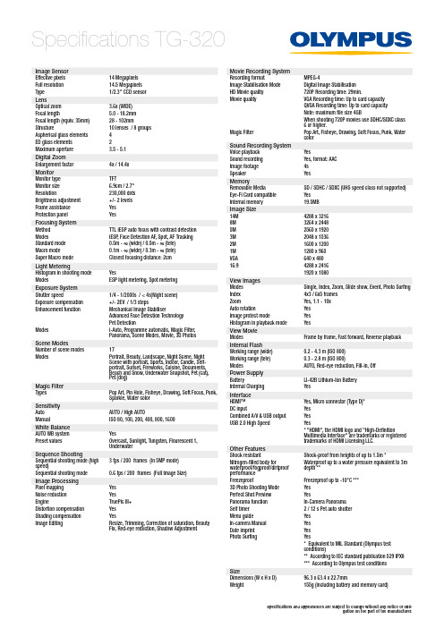
Specifications TG-320Specifications and appearances are subject to change without any notice or obli-gation on the part of the manufacturer.Image Sensor Effective pixels 14 Megapixels Full resolution 14.5 Megapixels Type1/2.3'' CCD sensor LensOptical zoom 3.6x (WIDE)Focal length5.0 - 18.2mm Focal length (equiv. 35mm)28 - 102mmStructure10 lenses / 8 groups Aspherical glass elements 4ED glass elements 2Maximum aperture 3.5 - 5.1Digital Zoom Enlargement factor 4x / 14.4x Monitor Monitor type TFTMonitor size 6.9cm / 2.7''Resolution230,000 dots Brightness adjustment +/- 2 levels Frame assistance Yes Protection panel YesFocusing System Method TTL iESP auto focus with contrast detection ModesiESP , Face Detection AF, Spot, AF Tracking Standard mode 0.5m - ∞ (wide) / 0.5m - ∞ (tele)Macro mode0.1m - ∞ (wide) / 0.3m - ∞ (tele)Super Macro mode Closest focusing distance: 2cm Light MeteringHistogram in shooting mode YesModesESP light metering, Spot metering Exposure System Shutter speed1/4 - 1/2000s / < 4s(Night scene)Exposure compensation +/- 2EV / 1/3 stepsEnhancement functionMechanical Image StabiliserAdvanced Face Detection Technology Pet DetectionModesi-Auto, Programme automatic, Magic Filter, Panorama, Scene Modes, Movie, 3D Photos Scene ModesNumber of scene modes 17ModesPortrait, Beauty, Landscape, Night Scene, Night Scene with portrait, Sports, Indoor, Candle, Self-portrait, Sunset, Fireworks, Cuisine, Documents, Beach and Snow, Underwater Snapshot, Pet (cat), Pet (dog)Magic Filter Types Pop Art, Pin Hole, Fisheye, Drawing, Soft Focus, Punk, Sparkle, Water colorSensitivity Auto AUTO / High AUTOManual ISO 80, 100, 200, 400, 800, 1600White Balance AUTO WB system YesPreset valuesOvercast, Sunlight, Tungsten, Flourescent 1, UnderwaterSequence ShootingSequential shooting mode (high speed)3 fps / 200 frames (in 5MP mode)Sequential shooting mode 0.6 fps / 200 frames (Full Image Size)Image Processing Pixel mapping Yes Noise reduction YesEngineTruePic III+ Distortion compensation Yes Shading compensation YesImage EditingResize, Trimming, Correction of saturation, Beauty Fix, Red-eye reduction, Shadow AdjustmentMovie Recording System Recording formatMPEG-4Image Stabilisation Mode Digital Image Stabilisation HD Movie quality 720P Recording time: 29min.Movie qualityVGA Recording time: Up to card capacity QVGA Recording time: Up to card capacity Note: maximum file size 4GBWhen shooting 720P movies use SDHC/SDXC class 6 or higher.Magic FilterPop Art, Fisheye, Drawing, Soft Focus, Punk, Water colorSound Recording System Voice playback YesSound recording Yes, format: AAC Image footage 4s SpeakerYesMemoryRemovable MediaSD / SDHC / SDXC (UHS speed class not supported)Eye-Fi Card compatible Yes Internal memory 19.5MB Image Size 14M 4288 x 32168M 3264 x 24485M 2560 x 19203M 2048 x 15362M 1600 x 12001M 1280 x 960VGA 640 x 48016:94288 x 24161920 x 1080View Images Modes Single, Index, Zoom, Slide show, Event, Photo Surfing Index 4x3 / 6x5 frames ZoomYes, 1.1 - 10x Auto rotationYes Image protect modeYes Histogram in playback mode YesView Movie ModesFrame by frame, Fast forward, Reverse playback Internal Flash Working range (wide)0.2 - 4.3 m (ISO 800) Working range (tele)0.3 - 2.8 m (ISO 800)ModesAUTO, Red-eye reduction, Fill-in, Off Power Supply BatteryLI-42B Lithium-Ion Battery Internal ChargingYesInterface HDMI™Yes, Micro connector (Type D)*DC inputYes Combined A/V & USB output Yes USB 2.0 High SpeedYes* "HDMI", the HDMI logo and "High-DefinitionMultimedia Interface" are trademarks or registered trademarks of HDMI Licensing LLC.Other Features Shock resistantShock-proof from heights of up to 1.5m *Nitrogen-filled body forwaterproof/fogproof/dirtproof performance Waterproof up to a water pressure equivalent to 3m depth **FreezeproofFreezeproof up to -10°C ***3D Photo Shooting Mode Yes Perfect Shot Preview YesPanorama function In-Camera Panorama Self timer 2 / 12 s Pet auto shutter Menu guideYes In-camera Manual Yes Date imprint Yes Photo SurfingYes* Equivalent to MIL Standard (Olympus test conditions)** According to IEC standard publication 529 IPX8*** According to Olympus test conditions SizeDimensions (W x H x D)96.3 x 63.4 x 22.7mmWeight155g (including battery and memory card)。
CS5341-CZZR中文资料

105 dB, 192 kHz, Multi-Bit Audio A/D ConverterFeaturesAdvanced Multi-bit Delta-Sigma Architecture 24-bit ConversionSupports All Audio Sample Rates Including192kHz105dB Dynamic Range at 5V -98dB THD+N90 mW Power ConsumptionHigh-Pass Filter to Remove DC Offsets Analog/Digital Core Supplies from 3.3V to 5V Supports Logic Levels between 1.8V and 5V Auto-Detect Mode Selection in Slave Mode Auto-Detect MCLK DividerGeneral DescriptionThe CS5341 is a complete analog-to-digital converter for digital audio systems. It performs sampling, analog-to-digital conversion, and anti-alias filtering, generating 24-bit values for both left and right inputs in serial form at sample rates up to 200kHz per channel.The CS5341 uses a 5th-order, multi-bit Delta-Sigma modulator followed by digital filtering and decimation,which removes the need for an external anti-alias filter. The CS5341 is available in a 16-pin TSSOP package for Commercial (-10° to +70° C) and Automotive grades (-40° to +85° C). The CDB5341 Customer Demonstra-tion Board is also available for device evaluation and implementation suggestions. Please refer to “Ordering Information” on page 22 for complete ordering information.The CS5341 is ideal for audio systems requiring wide dynamic range, negligible distortion and low noise, such as set-top boxes, DVD-karaoke players, DVD record-ers, A/V receivers, and automotive applications.CS5341CS5341 TABLE OF CONTENTS1. CHARACTERISTICS AND SPECIFICATIONS (4)SPECIFIED OPERATING CONDITIONS (4)ABSOLUTE MAXIMUM RATINGS (4)ANALOG CHARACTERISTICS - COMMERCIAL GRADE (5)ANALOG CHARACTERISTICS - AUTOMOTIVE GRADE (6)DIGITAL FILTER CHARACTERISTICS (7)DC ELECTRICAL CHARACTERISTICS (10)DIGITAL CHARACTERISTICS (10)SWITCHING CHARACTERISTICS - SERIAL AUDIO PORT (11)2. PIN DESCRIPTION (13)3. TYPICAL CONNECTION DIAGRAM (14)4. APPLICATIONS (15)4.1 Single-, Double-, and Quad-Speed Modes (15)4.2 Operation as Either a Clock Master or Slave (15)4.2.1 Operation as a Clock Master (16)4.2.2 Operation as a Clock Slave with Auto-Detect (16)4.2.3 Master Clock (17)4.3 Serial Audio Interface (17)4.4 Power-Up Sequence (18)4.5 Analog Connections (18)4.6 Grounding and Power Supply Decoupling (18)4.7 Synchronization of Multiple Devices (18)4.8 Capacitor Size on the Reference Pin (FILT+) (19)5. PARAMETER DEFINITIONS (20)6. PACKAGE DIMENSIONS (21)THERMAL CHARACTERISTICS (21)7. ORDERING INFORMATION (22)8. REVISION HISTORY (22)CS5341 LIST OF FIGURESFigure 1.Single-Speed Mode Stopband Rejection (8)Figure 2.Single-Speed Mode Stopband Rejection (8)Figure 3.Single-Speed Mode Transition Band (Detail) (8)Figure 4.Single-Speed Mode Passband Ripple (8)Figure 5.Double-Speed Mode Stopband Rejection (8)Figure 6.Double-Speed Mode Stopband Rejection (8)Figure 7.Double-Speed Mode Transition Band (Detail) (9)Figure 8.Double-Speed Mode Passband Ripple (9)Figure 9.Quad-Speed Mode Stopband Rejection (9)Figure 10.Quad-Speed Mode Stopband Rejection (9)Figure 11.Quad-Speed Mode Transition Band (Detail) (9)Figure 12.Quad-Speed Mode Passband Ripple (9)Figure 13.Master Mode, Left-Justified SAI (12)Figure 14.Slave Mode, Left-Justified SAI (12)Figure 15.Master Mode, I²S SAI (12)Figure 16.Slave Mode, I²S SAI (12)Figure 17.Typical Connection Diagram (14)Figure 18.CS5341 Master Mode Clocking (16)Figure 19.I²S Serial Audio Interface (17)Figure 20.Left-Justified Serial Audio Interface (17)Figure 21.CS5341 Recommended Analog Input Buffer (18)Figure 22.CS5341 THD+N versus Frequency (19)LIST OF TABLESTable 1. Speed Modes and the Associated Output Sample Rates (Fs) (15)Table 2. CS5341 Mode Control (15)Table 3. Master Clock (MCLK) Ratios (17)Table 4. Master Clock (MCLK) Frequencies for Standard Audio Sample Rates (17)CS53411.CHARACTERISTICS AND SPECIFICATIONS(All Min/Max characteristics and specifications are guaranteed over the Specified Operating Conditions. Typical performance characteristics and specifications are derived from measurements taken at typical supply voltages and T A = 25°C.)SPECIFIED OPERATING CONDITIONS(GND = 0V, all voltages with respect to 0V.)Notes:1.This part is specified at typical analog voltages of 3.3 V and 5.0 V. See Analog Characteristics - Com-mercial Grade and Analog Characteristics - Automotive Grade, below, for details.ABSOLUTE MAXIMUM RATINGS(GND = 0 V, All voltages with respect to ground.) (Note 2)2.Operation beyond these limits may result in permanent damage to the device.Normal operation is not guaranteed at these extremes.3.Any pin except supplies. Transient currents of up to ±100mA on the analog input pins will not causeSRC latch-up.4.The maximum over/under voltage is limited by the input current.ParameterSymbol Min TypMaxUnitPower SuppliesAnalog Digital Logic VA VD VL 3.13.11.7(Note 1)3.33.35.255.255.25V V V Ambient Operating TemperatureCommercial AutomotiveT AC T AC-10-40--7085°C °CParameterSymbol Min Max Units DC Power Supplies:Analog Logic Digital VA VL VD -0.3-0.3-0.3+6.0+6.0+6.0V V V Input Current (Note 3)I in -10+10mA Analog Input Voltage (Note 4)V IN GND-0.7VA+0.7V Digital Input Voltage(Note 4)V IND-0.7VL+0.7VAmbient Operating Temperature (Power Applied)T A-50+95°CStorage TemperatureT stg-65+150°CCS5341ANALOG CHARACTERISTICS - COMMERCIAL GRADETest Conditions (unless otherwise specified): Input test signal is a 1 kHz sine wave; measurement bandwidth is 10 Hz to 20 kHz.5.Referred to the typical full-scale input voltageDynamic Performance for Commercial Grade VA = 5 V VA = 3.3 VSingle-Speed Mode Fs = 48kHzSymbol MinTypMaxMinTypMaxUnitDynamic RangeA-weighted unweighted 9996105102--969310299--dB dBTotal Harmonic Distortion + Noise(Note 5) -1dB -20dB -60dBTHD+N----98-82-42-92------95-79-39-89--dB dB dBDouble-Speed Mode Fs = 96kHzSymbol MinTypMaxMinTypMaxUnitDynamic RangeA-weighted unweighted40kHz bandwidth unweighted 9996-10510299---9693-1029996---dB dB dBTotal Harmonic Distortion + Noise (Note 5) -1dB -20dB -60dB40kHz bandwidth -1dBTHD+N-----98-82-42-95-92--------95-79-39-87-89---dB dB dB dBQuad-Speed Mode Fs = 192kHzSymbol MinTypMaxMinTypMaxUnitDynamic RangeA-weighted unweighted40kHz bandwidth unweighted 9996-10510299---9693-1029996---dB dB dBTotal Harmonic Distortion + Noise (Note 5) -1dB -20dB -60dB40kHz bandwidth -1dBTHD+N-----98-82-42-95-92--------95-79-39-87-89---dB dB dB dBDynamic Performance All ModesMinTypMaxUnitInterchannel Isolation-90-dBDC AccuracyInterchannel Gain Mismatch -0.1-dB Gain Error -5-+5%Gain Drift-±100-ppm/°CAnalog Input CharacteristicsFull-Scale Input Voltage 0.53*VA0.56*VA 0.59*VAVppInput Impedance-25-k ΩCS5341ANALOG CHARACTERISTICS - AUTOMOTIVE GRADETest Conditions (unless otherwise specified): Input test signal is a 1 kHz sine wave; measurement bandwidth is 10 Hz to 20 kHz.6.Referred to the typical full-scale input voltageDynamic Performance for Automotive Grade VA = 5 V VA = 3.3 VSingle-Speed Mode Fs = 48kHzSymbol MinTypMaxMinTypMaxUnitDynamic RangeA-weighted unweighted 9794105102--949110299--dB dBTotal Harmonic Distortion + Noise(Note 6) -1dB -20dB -60dBTHD+N----98-82-42-90------95-79-39-87--dB dB dBDouble-Speed Mode Fs = 96kHzSymbol MinTypMaxMinTypMaxUnitDynamic RangeA-weighted unweighted40kHz bandwidth unweighted 9794-10510299---9491-1029996---dB dB dBTotal Harmonic Distortion + Noise (Note 6) -1dB -20dB -60dB40kHz bandwidth -1dBTHD+N-----98-82-42-95-90--------95-79-39-87-87---dB dB dB dBQuad-Speed Mode Fs = 192kHzSymbol MinTypMaxMinTypMaxUnitDynamic RangeA-weighted unweighted40kHz bandwidth unweighted 9794-10510299---9491-1029996---dB dB dBTotal Harmonic Distortion + Noise (Note 6) -1dB -20dB -60dB40kHz bandwidth -1dBTHD+N-----98-82-42-95-90--------95-79-39-87-87---dB dB dB dBDynamic Performance All ModesMinTypMaxUnitInterchannel Isolation-90-dBDC AccuracyInterchannel Gain Mismatch -0.1-dB Gain Error -10-+10%Gain Drift-±100-ppm/°CAnalog Input CharacteristicsFull-Scale Input Voltage 0.50*VA0.56*VA 0.62*VAVppInput Impedance-25-k ΩCS5341DIGITAL FILTER CHARACTERISTICS7.Filter characteristics scale precisely with Fs8.Response shown is for Fs equal to 48 kHz. Filter characteristics scale with Fs.ParameterSymbol Min Typ Max UnitSingle-Speed ModePassband (-0.1 dB)(Note 7)0-0.4895Fs Passband Ripple -0.035-0.035dB Stopband(Note 7)0.5687--Fs Stopband Attenuation70--dB Total Group Delay (Fs = Output Sample Rate)t gd-12/Fs -s Double-Speed ModePassband (-0.1 dB)(Note 7)0-0.4895Fs Passband Ripple -0.025-0.025dB Stopband(Note 7)0.5604--Fs Stopband Attenuation69--dB Total Group Delay (Fs = Output Sample Rate)t gd-9/Fs -s Quad-Speed ModePassband (-0.1 dB)(Note 7)0-0.2604Fs Passband Ripple -0.025-0.025dB Stopband(Note 7)0.5--Fs Stopband Attenuation60--dB Total Group Delay (Fs = Output Sample Rate)t gd-5/Fs -s High-Pass Filter CharacteristicsFrequency Response -3.0 dB -0.13 dB (Note 8)-120--Hz Hz Phase Deviation @ 20Hz(Note 8)-10-Deg Passband Ripple--0dBFigure 1. Single-Speed Mode Stopband Rejection Figure 2. Single-Speed Mode Stopband RejectionFigure 5. Double-Speed Mode Stopband Rejection Figure 6. Double-Speed Mode Stopband RejectionCS5341Figure 7. Double-Speed Mode Transition Band (Detail)Figure 8. Double-Speed Mode Passband RippleFigure 9. Quad-Speed Mode Stopband Rejection Figure 10. Quad-Speed Mode Stopband RejectionFigure 11. Quad-Speed Mode Transition Band (Detail)Figure 12. Quad-Speed Mode Passband RippleCS5341DC ELECTRICAL CHARACTERISTICS(GND = 0V, all voltages with respect to 0V. MCLK=12.288MHz; Master Mode)9.Power-Down Mode is defined as RST = Low, with all clocks and data lines held static at a valid logiclevels.10.Valid with the recommended capacitor values on FILT+ and VQ as shown in the Typical ConnectionDiagram.DIGITAL CHARACTERISTICSParameterSymbolMinTypMaxUnitDC Power Supplies:Positive Analog Positive DigitalPositive LogicVA VD VL 3.13.11.7--- 5.255.255.25V V V Power Supply CurrentVA = 5 V (Normal Operation)VA = 3.3 V VL,VD = 5V VL,VD = 3.3VI A I A I D I D ----2118.215925.522.518.510mA mA mA mA Power Supply CurrentVA = 5V (Power-Down Mode) (Note 9)VL,VD=5VI A I D -- 1.50.4--mA mA Power Consumption VL, VD, VA = 5V (Normal Operation)VL, VD, VA = 3.3V (Power-Down Mode)------180909.5220107.2-mW mW mW Power Supply Rejection Ratio (1kHz)(Note 10)PSRR-65-dB V Q Nominal Voltage Output Impedance--VA ÷225--V k ΩFilt+ Nominal Voltage Output ImpedanceMaximum allowable DC current source/sink---VA 360.01---V k ΩmAParameterSymbolMinTypMaxUnitsHigh-Level Input Voltage (% of VL)V IH 70%--V Low-Level Input Voltage(% of VL)V IL --30%V High-Level Output Voltage at I o = 100µA (% of VL)V OH 70%--V Low-Level Output Voltage at I o =100µA (% of VL)V OL --15%V Input Leakage CurrentI in-10-+10µACS5341SWITCHING CHARACTERISTICS - SERIAL AUDIO PORT(Logic "0" = GND = 0V; Logic "1" = VL, C L = 20pF)11. For a description of speed modes, please refer to Table 1 on page 15.Parameter Symbol Min Typ Max UnitMCLK SpecificationsMCLK Periodt clkw39-45ns 78-1953ns MCLK Pulse Duty Cycle40-60%Master ModeSCLK falling to LRCKSingle-Speed t mslr-20-20ns Double-Speed -20-20ns Quad-Speed-8-8ns SCLK falling to SDOUT valid. t sdo--32ns SCLK Duty Cycle.Single-Speed -50-%Double-Speed -50-%Quad-Speed-33-%Slave ModeSingle-Speed (Note 11)LRCK Duty Cycle 405060%SCLK Period t sclkw156--ns SCLK Duty Cycle455055%SDOUT valid before SCLK rising t stp 10--ns SDOUT valid after SCLK rising t hld 5--ns SCLK falling to LRCK edget slrd -20-20ns Double-Speed (Note 11)LRCK Duty Cycle 405060%SCLK Period t sclkw156--ns SCLK Duty Cycle455055%SDOUT valid before SCLK rising t stp 10--ns SDOUT valid after SCLK rising t hld 5--ns SCLK falling to LRCK edge.t slrd-20-20ns Quad-Speed (Note 11)LRCK Duty Cycle 405060%SCLK Period t sclkw78--ns SCLK Duty Cycle29.73350%SDOUT valid before SCLK rising t stp 10--ns SDOUT valid after SCLK rising t hld 5--ns SCLK falling to LRCK edge.t slrd-8-8nsCS5341Figure 13. Master Mode, Left-Justified SAI Figure 14. Slave Mode, Left-Justified SAIFigure 15. Master Mode, I²S SAI Figure 16. Slave Mode, I²S SAICS5341 2.PIN DESCRIPTIONPin Name#Pin DescriptionM0 M1116Mode Selection (Input) - Determines the operational mode of the device.MCLK2Master Clock (Input) - Clock source for the delta-sigma modulator and digital filters. VL3Logic Power (Input) - Positive power for the digital input/output.SDOUT4Serial Audio Data Output (Output) - Output for two’s complement serial audio data. GND5,14Ground (Input) - Ground reference. Must be connected to analog ground.VD6Digital Power (Input) - Positive power supply for the digital section.SCLK7Serial Clock (Input/Output) - Serial clock for the serial audio interface.LRCK8Left Right Clock (Input/Output) - Determines which channel, Left or Right, is currently active on the serial audio data line.RST9Reset (Input) - The device enters a low power mode when low.AINL AINR 1012Analog Input (Input) - The full-scale analog input level is specified in the Analog Charac-teristics specification table.VQ11Quiescent Voltage (Output) - Filter connection for the internal quiescent reference voltage.VA13Analog Power (Input) - Positive power supply for the analog section.FILT+15Positive Voltage Reference (Output) - Positive reference voltage for the internal sampling circuits.M0M1MCLK FILT+VL REF_GNDSDOUT VAGND AINRVD VQSCLK AINLLRCK RST11634785261514131211109CS5341 3.TYPICAL CONNECTION DIAGRAMCS53414.APPLICATIONS4.1Single-, Double-, and Quad-Speed ModesThe CS5341 can support output sample rates from 2kHz to 200kHz. The proper speed mode can be de-termined by the desired output sample rate and the external MCLK/LRCK ratio, as shown in Table 1.Table 1. Speed Modes and the Associated Output Sample Rates (Fs)4.2Operation as Either a Clock Master or SlaveThe CS5341 supports operation as either a clock master or slave. As a clock master, the LRCK and SCLK pins are outputs with the left/right and serial clocks synchronously generated on-chip. As a clock slave, the LRCK and SCLK pins are inputs and require the left/right and serial clocks to be externally generated. The selection of clock master or slave is made via the Mode pins as shown in Table 2.Speed ModeMCLK/LRCKRatioOutput Sample Rate Range (kHz)Single-Speed Mode 512x 43 - 50256x 2 - 50Double-Speed Mode 256x 86 - 100128x 50 - 100Quad-Speed Mode128x 172 - 20064x*100 - 200* Quad-Speed Mode, 64x only available in Master Mode.M1 (Pin 16)M0 (Pin 1)MODE00Clock Master, Single-Speed Mode 01Clock Master, Double-Speed Mode 10Clock Master, Quad-Speed Mode 11Clock Slave, All Speed ModesTable 2. CS5341 Mode ControlCS53414.2.1Operation as a Clock MasterAs a clock master, LRCK and SCLK operate as outputs. The left/right and serial clocks are internally de-rived from the master clock with the left/right clock equal to Fs and the serial clock equal to 64x Fs, as shown in Figure 18.4.2.2Operation as a Clock Slave with Auto-DetectLRCK and SCLK operate as inputs in clock Slave Mode. It is recommended that the left/right clock be synchronously derived from the master clock and must be equal to Fs. It is also recommended that the serial clock be synchronously derived from the master clock and be equal to 64x Fs to maximize system performance.A unique feature of the CS5341 is the automatic selection of either Single-, Double- or Quad-Speed Mode when operating as a clock slave. The auto-mode select feature negates the need to configure the Mode pins to correspond to the desired mode. The auto-mode selection feature supports all standard audio sample rates from 2 to 200kHz. However, there are ranges of non-standard audio sample rates that are not supported when operating with a fast MCLK (512x, 256x, 128x for Single-, Double-, and Quad-Speed Modes, respectively). Please refer to Table 1 for supported sample rate ranges.Figure 18. CS5341 Master Mode ClockingCS53414.2.3Master ClockThe CS5341 requires a Master clock (MCLK) which runs the internal sampling circuits and digital filters.There is also an internal MCLK divider which is automatically activated based on the speed mode and frequency of the MCLK. Table 3 shows a listing of the external MCLK/LRCK ratios that are required.Table 4 lists some common audio output sample rates and the required MCLK frequency. Please note that not all of the listed sample rates are supported when operating with a fast MCLK (512x, 256x, 128x for Single-, Double-, and Quad-Speed Modes, respectively).4.3Serial Audio InterfaceThe CS5341 supports both I²S and Left-Justified serial audio formats. Upon start-up, the CS5341 will detect the logic level on SDOUT (pin 4). A 10 k Ω pull-up to VL is needed to select I²S format, and a 10 k Ω pull-down to GND is needed to select Left-Justified format. Figures 19 and 20 illustrate the I²S and Left-Justified audio formats. Please see Figures 13 through 16, for more information on the required timing for the two serial audio interface formats. Also see Application Note AN282 for a detailed discussion of the serial audioSingle-Speed ModeDouble-Speed ModeQuad-Speed ModeMCLK/LRCK Ratio256x, 512x128x, 256x64x*,128x* Quad Speed, 64x only available in Master Mode.Table 3. Master Clock (MCLK) RatiosSAMPLE RATE (kHz)MCLK (MHz)328.192 44.111.289622.57924812.28824.576648.19288.211.289622.57929612.28824.57619212.28824.576Table 4. Master Clock (MCLK) Frequencies for Standard Audio Sample RatesCS5341 4.4Power-Up SequenceReliable power-up can be accomplished by keeping the device in reset until the power supplies, clocks andconfiguration pins are stable. It is also recommended that reset be enabled if the analog or digital suppliesdrop below the minimum specified operating voltages to prevent power-glitch-related issues.4.5Analog ConnectionsThe analog modulator samples the input at half of the MCLK frequency, or nominally 6.144MHz. The digitalfilter will reject signals within the stopband of the filter. However, there is no rejection for input signals whichare multiples of the input sampling frequency (n×6.144MHz), where n=0,1,2,... Refer to Figure21, which shows the suggested filter that will attenuate any noise energy at 6.144MHz in addition to providing the op-timum source impedance for the modulators. The use of capacitors that have a large voltage coefficient(such as general-purpose ceramics) must be avoided since these can degrade signal linearity. Array4.6Grounding and Power Supply DecouplingAs with any high resolution converter, achieving optimal performance from the CS5341 requires careful at-tention to power supply and grounding arrangements. Figure17 shows the recommended power arrange-ments, with VA and VL connected to clean supplies. VD, which powers the digital filter, may be run from thesystem logic supply or may be powered from the analog supply via a resistor. In this case, no additionaldevices should be powered from VD. Decoupling capacitors should be as near to the ADC as possible, withthe low-value ceramic capacitor being the nearest. All signals, especially clocks, should be kept away fromthe FILT+ and VQ pins in order to avoid unwanted coupling into the modulators. The FILT+ and VQ decou-pling capacitors, particularly the 0.01µF, must be positioned to minimize the electrical path from FILT+ andREF_GND. Furthermore, all ground pins on CS5341 should be referenced to the same ground reference.The CDB5341 evaluation board demonstrates the optimum layout and power supply arrangements. To min-imize digital noise, connect the ADC digital outputs only to CMOS inputs.4.7Synchronization of Multiple DevicesIn systems where multiple ADCs are required, the user can achieve simultaneous sampling if the MCLK andLRCK signals are the same for all of the CS5341’s in the system. If only one master clock source is needed,one solution is to place one CS5341 in Master Mode, and slave all of the other CS5341’s to the one master.If multiple master clock sources are needed, a possible solution would be to supply all clocks from the sameexternal source and time the CS5341 reset with the inactive (falling) edge of MCLK. This will ensure that allconverters begin sampling on the same clock edge.CS53414.8Capacitor Size on the Reference Pin (FILT+)The CS5341 requires an external capacitance on the internal reference voltage pin, FILT+. The size of this decoupling capacitor will affect the low frequency distortion performance as shown in Figure 22, with larger capacitor values used to optimize low frequency distortion performance. This plot was taken using the CDB5341 evaluation platform, with the device running in Single-Speed Mode and VA=VD=VL=5 V.Figure 22. CS5341 THD+N versus Frequency47 uF100 uF22 uF10 uF6.8 uF4.7 uF3.3 uF2.2 uF1 uF5.6 uFCS5341 5.PARAMETER DEFINITIONSDynamic RangeThe ratio of the rms value of the signal to the rms sum of all other spectral components over the specified bandwidth. Dynamic Range is a signal-to-noise ratio measurement over the specified bandwidth made witha -60dBFS signal. 60dB is added to resulting measurement to refer the measurement to full-scale. Thistechnique ensures that the distortion components are below the noise level and do not affect the measure-ment. This measurement technique has been accepted by the Audio Engineering Society, AES17-1991, and the Electronic Industries Association of Japan, EIAJ CP-307. Expressed in decibels.Total Harmonic Distortion + NoiseThe ratio of the rms value of the signal to the rms sum of all other spectral components over the specified bandwidth (typically 10Hz to 20kHz), including distortion components. Expressed in decibels. Measured at -1 and -20dBFS as suggested in AES17-1991 Annex A.Frequency ResponseA measure of the amplitude response variation from 10Hz to 20kHz relative to the amplitude response at1kHz. Units in decibels.Interchannel IsolationA measure of crosstalk between the left and right channels. Measured for each channel at the converter'soutput with no signal to the input under test and a full-scale signal applied to the other channel. Units in deci-bels.Interchannel Gain MismatchThe gain difference between left and right channels. Units in decibels.Gain ErrorThe deviation from the nominal full-scale analog input for a full-scale digital output.Gain DriftThe change in gain value with temperature. Units in ppm/°C.Offset ErrorThe deviation of the mid-scale transition (111...111 to 000...000) from the ideal. Units in mV.DS564F121CS53416.PACKAGE DIMENSIONS1.“D” and “E1” are reference datums and do not included mold flash or protrusions, but do include moldmismatch and are measured at the parting line, mold flash or protrusions shall not exceed 0.20mm per side.2.Dimension “b” does not include dambar protrusion/intrusion. Allowable dambar protrusion shall be0.13mm total in excess of “b” dimension at maximum material condition. Dambar intrusion shall not re-duce dimension “b” by more than 0.07mm at least material condition.3.These dimensions apply to the flat section of the lead between 0.10 and 0.25mm from lead tips.THERMAL CHARACTERISTICSINCHES MILLIMETERSNOTEDIM MIN NOM MAX MIN NOM MAX A ----0.043---- 1.10A10.0020.0040.0060.05--0.15A20.033460.03540.0370.850.900.95b 0.007480.00960.0120.190.2450.302,3D 0.1930.19690.201 4.90 5.00 5.101E 0.2480.25190.256 6.30 6.40 6.50E10.1690.17320.177 4.30 4.40 4.501e --0.026 BSC ----0.65 BSC --L 0.0200.0240.0280.500.600.70µ0°4°8°0°4°8°JEDEC #: MO-153Controlling Dimension is MillimetersParameterSymbol MinTypMaxUnit Allowable Junction Temperature --135°C Junction to Ambient Thermal ImpedanceθJA-75-°C/W16L TSSOP (4.4mm BODY) PACKAGE DRAWINGEN123eb 2A1A2ADSEATING PLANE E11LSIDE VIEWEND VIEWTOP VIEW∝22DS564F1CS53417.ORDERING INFORMATION8.REVISION HISTORYProductDescription Package Pb-Free Grade Temp Range ContainerOrder #CS5341105 dB, 192 kHz, Multi-BitAudio A/D Converter 16-TSSOP YES Commercial -10° to +70° CBulk CS5341-CZZ Tape & ReelCS5341-CZZR CS5341105 dB, 192 kHz, Multi-BitAudio A/D Converter 16-TSSOP YES Automotive -40° to +85° CBulk CS5341-DZZ Tape & ReelCS5341-DZZR CDB5341 CS5341 Evaluation Board -----CDB5341ReleaseChangesA1Initial Advance releaseA2Updated serial port timing specificationsPP1Change value of capacitors in analog input buffer diagram Update Sample Rate rangeAdded Applications section on FILT+ filter capacitor Add CS5341-CZZ as part numberReplace available part number CS5341-DZ with CS5341-DZZ Initial Preliminary product releasePP2Add lead-free option to ordering information F1Remove CS5341-CZ from Ordering InformationRedefine Serial Audio Port Switching Characteristics Correct dimension “e” under Package Dimensions Update maximum current and power specifications Update Filt+ output impedance specificationContacting Cirrus Logic SupportFor all product questions and inquiries, contact a Cirrus Logic Sales Representative. To find the one nearest to you, go to .IMPORTANT NOTICECirrus Logic, Inc. and its subsidiaries ("Cirrus") believe that the information contained in this document is accurate and reliable. However, the information is subject to change without notice and is provided "AS IS" without warranty of any kind (express or implied). Customers are advised to obtain the latest version of relevant information to verify, before placing orders, that information being relied on is current and complete. All products are sold subject to the terms and conditions of sale supplied at the time of order acknowledgment, including those pertaining to warranty, indemnification, and limitation of liability. No responsibility is assumed by Cirrus for the use of this information, including use of this information as the basis for manufacture or sale of any items, or for infringement of patents or other rights of third parties. This document is the property of Cirrus and by furnishing this information, Cirrus grants no license, express or implied under any patents, mask work rights,copyrights, trademarks, trade secrets or other intellectual property rights. Cirrus owns the copyrights associated with the information contained herein and gives con-sent for copies to be made of the information only for use within your organization with respect to Cirrus integrated circuits or other products of Cirrus. This consent does not extend to other copying such as copying for general distribution, advertising or promotional purposes, or for creating any work for resale.CERTAIN APPLICATIONS USING SEMICONDUCTOR PRODUCTS MAY INVOLVE POTENTIAL RISKS OF DEATH, PERSONAL INJURY, OR SEVERE PROP-ERTY OR ENVIRONMENTAL DAMAGE (“CRITICAL APPLICATIONS”). CIRRUS PRODUCTS ARE NOT DESIGNED, AUTHORIZED OR WARRANTED FOR USE IN AIRCRAFT SYSTEMS, MILITARY APPLICATIONS, PRODUCTS SURGICALLY IMPLANTED INTO THE BODY, AUTOMOTIVE SAFETY OR SECURITY DE-VICES, LIFE SUPPORT PRODUCTS OR OTHER CRITICAL APPLICATIONS. INCLUSION OF CIRRUS PRODUCTS IN SUCH APPLICATIONS IS UNDER-STOOD TO BE FULLY AT THE CUSTOMER’S RISK AND CIRRUS DISCLAIMS AND MAKES NO WARRANTY, EXPRESS, STATUTORY OR IMPLIED,INCLUDING THE IMPLIED WARRANTIES OF MERCHANTABILITY AND FITNESS FOR PARTICULAR PURPOSE, WITH REGARD TO ANY CIRRUS PRODUCT THAT IS USED IN SUCH A MANNER. IF THE CUSTOMER OR CUSTOMER’S CUSTOMER USES OR PERMITS THE USE OF CIRRUS PRODUCTS IN CRITICAL APPLICATIONS, CUSTOMER AGREES, BY SUCH USE, TO FULLY INDEMNIFY CIRRUS, ITS OFFICERS, DIRECTORS, EMPLOYEES, DISTRIBUTORS AND OTHER AGENTS FROM ANY AND ALL LIABILITY, INCLUDING ATTORNEYS’ FEES AND COSTS, THAT MAY RESULT FROM OR ARISE IN CONNECTION WITH THESE USES.Cirrus Logic, Cirrus, and the Cirrus Logic logo designs are trademarks of Cirrus Logic, Inc. All other brand and product names in this document may be trademarks or service marks of their respective owners.I²C is a registered trademark of Philips Semiconductor.。
玉米单倍体育种技术研究进展及展望

宁夏农林科技,基金项目:宁夏农林科学院自主研发项目(DWHZC-2017007)。
作者简介:佘奎军(1982-),男,宁夏平罗人,副研究员,硕士研究生,主要从事玉米遗传育种工作。
E-mail:通信作者:杨国虎(1970-),男,宁夏银川人,博士,研究员,主要从事玉米遗传育种工作。
E-mail:收稿日期:2020-04-26修回日期:2021-06-091单倍体的发现及单倍体诱导系的选育玉米单倍体育种技术研究进展及展望佘奎军1,刘艳妮2,程晋龙1,杨国虎11.宁夏农林科学院农作物研究所,宁夏银川750002;2.银川能源学院,宁夏永宁750105摘要:玉米是重要的粮食、饲料作物,以及医药、工业原料。
选育优质高产的玉米杂交种对保障粮食安全,推动畜牧业的发展和保障工业原料的持续供给具有非常重要的作用。
单倍体育种技术是利用诱导系诱导产生孤雌生殖单倍体,单倍体加倍后可以快速获得纯系。
利用该技术可加快玉米自交系选育进程,提高选育效率。
文章阐述了单倍体育种的关键技术,包括单倍体诱导系的选育、单倍体诱导的机理、影响单倍体诱导率的因素、单倍体的鉴定方法、单倍体加倍的条件,分析了单倍体育种技术存在的问题,展望了玉米单倍体育种技术应用前景。
关键词:玉米;单倍体育种技术;诱导系中图分类号:S513文献标识码:A文章编号:1002-204X (2021)10-0025-06doi:10.3969/j.issn.1002-204x.2021.10.007Research Progress in Double Haploid Breeding Technology of MaizeAbstract Key words 2562卷10期R njABPI2产生单倍体诱导的机制qhirBqhirMATRILINEL MATLZmPLA NOTLIKE DAD NLDZmPLA MATRILINEL MATL NOT LIKE DAD NLDqhirZmDMP ZmPLA ZmDMPZmDMP3单倍体的诱导率及其影响因素佘奎军,等玉米单倍体育种技术研究进展及展望264单倍体的鉴定方法R njR njR njR nj R njR njR nj6单倍体育种技术存在的问题及展望R njABPI5单倍体的二倍体化方法CRISPR CasgRNACRISPR Cas参考文献:[1]CHASE S S.Selection for parthenogenesis and monoploids[J].Agronomia,1952,44:263-267.[2]COE E H.A line of maize with high haploid frequency[J].The American Naturalist,1959,93:381-382.[3]KERMICLE J L.Androgenesis conditioned by a mutationin maize[J].Science,1969,166:1422-1424.[4]LASHERMES P,BECKERT M.Genetic control ofmaternal haploidy in maize(Zea mays L.)and selection of haploid inducing lines[J].Theoretical&Applied Genetics,1988,76:405-410.[5]CHALYK S T.Creating new haploid-inducing lines ofmaize[J].Maize Genet Coop Newslet,1999,73:53.[6]Röber F K,GORDILLO G A,GEIGER H H.Invivo haploid induction in maize-performance of new inducers and significance of doubled haploid lines in hybrid breeding[J].Maydica,2005,50:275.[7]CHEN S J,Song T M.Identification haploid withhigh oil xenia effect in maize[J].Acta Agronomica Sinica,2003,4:19.[8]CAI Z G,XU X H,LIU Y L et al.The breeding ofJAAS3-haploid inducer with high frequency partheno-genesis in maize[J].Jorunal of Maize Sciences,2007, 151:1-4.[9]LI L,LI H C,XU X W,et al.Preliminary optimiza-tion of in-vivo haploid induction in maize[J].Journal of China Agricultural University,2012,171:9-13.[10]李向永,姜龙,王薪淇,等.糯玉米单倍体诱导和加倍的研究[J].西北农林科技大学学报(自然科学版),2016,44(8):90-96.[11]WEBER D F.Today’s use of haploids in cornplant breeding[J].Advances in Agronomy,2014,123:123-144.[12]HU H,SCHRAG T A,PEIS R,et al.The geneticbasis of haploid induction in maize identified with anovel genome-wide association method[J].Genetics,2016,202:1267-1276.[13]PRIGGE V,MELCHINGER A E.Production ofhaploids and doubled haploids in maize[M].In:Loy-ola-Vargas VM,Ochoa-Alejo N(eds)Plant cellculture protocols.Berlin:Springer,2012:161-172. [14]DONG X,XU X,MIAO J,et al.Fine mapping ofqhir1influencing in vivo haploid induction in maize[M].Theoretical&Applied Genetics,2013,126:1713-1720.[15]SCHNABLE P S,WARE D,FULTON R S,et al.The B73maize genome:complexity,diversity,anddynamics[J].Science,2009,326:1112-1115.[16]KELLIHER T,STARR D,RICHBOURG L,et al.Matrilineal,a sperm specific phospholipase,triggersmaize haploid induction[J].Nature,2017,542:105-109.[17]LIU C,LI X,MENG D,et al.A4-bp insertion atZmPLA1encoding a putative phospholipase a gener-ates haploid induction in maize[J].Molecular Plant, 2017,10(3):520-522.[18]GILLES L M,KHALED A,LAFFAIRE J,et al.Losso f pollen‐specific phospholipase NOT LIKE DAD triggers gynogenesis in maize[J].The EMBO Journal, 2017,36:707-717.[19]ZHONG Y,LIU C X,QI X L.et al.Mutation ofZmDMP enhances haploid induction in maize[J].Nature Plants,2019,5:575-580.[20]KRIZ A L,LARKINS B A.Molecular genetic approachesto maize improvement[M].Berlin:Springer-Verlag,2009.[21]CHALYK S T.Creating new haploid-inducing linesof maize[J].Maize Genet Coop Newslet,1999,73:53 [22]ROTARENCO V A,DICU G,STAGE D,et al.New inducers of maternal haploids in maize[J].Maize Genet Coop Newsl,2010,84:15.[23]GEIGER H H.Doubled haploids.In:Bennetzen JL,Hake S(eds)Handbook of maize[M].New York: Springer,2009,641-657.[24]LIU Z Z,SONG T M.The breeding and identifica-tion of haploid inducer with high frequency parthenogenesis in maize[J].Acta Agronomica Sinica, 2000,26:570-574.[25]LASHERMES P,BECKERT M.Genetic control ofmaternal haploidy in maize(Zea mays L.)and selection of haploid inducing lines[J].Theoretical&Applied Genetics,1988,76:405-410.[26]EDER J,CHALYK S.In vivo haploid induction inmaize[J].Theoretical&Applied Genetics,2002,104: 703-708.[27]LI L,XU X,JIN W,et al.Morphological and molecu-lar evidences for DNA introgression in haploid induction via a high oil inducer CAUHOI in maize[J].Planta, 2009,230:367-376.[28]PRIGGE V,SCHIPPRACK W,MAHUKU G,et al.Development of in vivo haploid inducers for tropical maize breeding programs[J].Euphytica,2012,185: 481-490.[29]CHAIKAM V,NAIR S K,MARTINEZ L,et al.Marker-assisted breeding of improved maternal hap-loid inducers in maize for the tropical/subtropical regions[J].Front Plant Science,2018,9:1527.[30]刘志增,宋同明.玉米高频率孤雌生殖单倍体诱导系(上接第19页)[8]何进尚,柳伟祥,刘阳春,等.宁夏灵武市郝家桥镇农田土壤盐分含量的空间分布特点[J].安徽农学通报,2009,15(3):54-56.[9]黄绍文,金继运,杨俐苹,等.土壤养分空间变异的影响因素[M].金继运,白由路.精准农业与土壤养分管理.北京:中国大地出版社,2001.39-50.[10]何文寿,何进勤,王菊兰,等.宁夏引黄灌区春小麦不同生育期土壤有效氮磷钾养分含量的动态变化特点[J].西北农业学报,2006,15(3):54-59.责任编辑:达海莉的选育与鉴定[J].作物学报,2000,26(5):570-574. [31]SARKAR K R,PANKE S,SACHAN JKS.Devel-opment of maternal haploidy-inducer lines in maize (Zea mays L.)[J].Indian Journal Agricultural Sciences, 1972,42:781-786.[32]BELICUAS P,GUIMARAES C,PAIVA J,et al.An-drogenetic haploids and SSR markers as tools for the development of tropical maize hybrids[J].Euphytica, 2007,156:95-102.[33]Preciado-Ortiz R E,García-Lara S,Ortiz-Islas S,etal.Response of recurrent selection on yield,kernel oil content and fatty acid composition of subtropical maize populations[J].Field Crops Research,2013,142(20):27-35.[34]DONG X,XU X W,LI L,et al.Marker-assistedselection and evaluation of high oil in vivo haploid inducers in maize[J].Molecular Breeding,2014,34: 1147-1158.[35]MELCHINGER A E,SCHIPPRACK W,Würschum T,et al.Rapid and accurate identification of in vi-vo-induced haploid seeds based on oil content in maize[J].Scientific Reports,2013(3):2129.[36]YU W,BIRCHLER J A.A green fluorescent pro-tein-engineered haploid inducer line facilitates haploid mutant screens and doubled haploid breeding in maize [J].Molecular Breeding,2016,36:1-12.[37]MOLENAAR W S,de Oliveira Couto E G,PIEPHOH,et al.Early diagnosis of ploidy status in doubled haploid production of maize by stomata length and flow cytometry measurements[J].Plant Breeding,2019, 138(3):266-276.[38]CHOE E,CARBONERO C H,MULVANEY K,etal.Improving in vivo maize doubled haploid produc-tion efficiency through early detection of false positives [J].Plant Breeding,2012,131:399-401.[39]BLAKESLEE A F,AVERY A G.Methods of induc-ing chromosome doubling in plants by treatment with colchicine[J].Journal of Heredity,1937,28(12): 393-411.[40]MELCHINGER A E,BRAUNER P C,Böhm J,et al.In vivo haploid induction in maize:comparison of dif-ferent testing regimes for measuring haploid induction rates[J].Crop Science,2016,56:1127-1135.[41]MOLENAAR W S,SCHIPPRACK W,BRAUNET PC,et al.Haploid male fertility and spontaneous chro-mosome doubling evaluated in a diallel and recurrent selection experiment in maize[J].Theoretical and Ap-plied Genetics,2019,132:2273-2284.[42]魏俊杰,张晓丽,陈梅香,等.6叶期秋水仙素注射处理玉米单倍体的加倍效果研究[J].玉米科学,2007,15(4):49-51.[43]VIJAY C,WILLEM M,ALBRECHT E,et al.Dou-bled haploid technology for line development in maize:technical advances and prospects[J].Theoretical and Applied Genetics,2019,132:3227-3243.[44]WANG B,ZHU L,ZHAO B,et al.Developmentof a haploid-inducer mediated genome editing system for accelerating maize breeding[J].Molecular Plant, 2019,12(4):597-602.[45]KELLIHER T,STARR D,SU X,et al.One-stepgenome editing of elite crop germplasm during haploid induction[J].Nature Biotechnology,2019,37:287-292.责任编辑:达海莉。
非遗传承,触摸中国文化Intangible_Cultural_Heritage_Inheritanc

非遗传承,触摸中国文化文/王天宇有祭孔大典的庄重威严,也有蹴鞠技艺的欢脱喜悦;有木版年画的艺术韵味,也有潍坊风筝的匠心独具;有梁祝传说的凄美婉转,也有胶州秧歌的普天同庆;有聊城杂技的翻转腾挪,也有山东快书的嬉笑怒骂……在这片历史悠久的齐鲁大地上,从来不缺乏人民的艺术,艺术的人民。
几张纸,一把剪刀,伴着“咔嚓咔嚓”的剪纸声,生动活泼的形象跃然纸上。
山东各地都有剪纸的风俗,以高密剪纸为例,其包括窗花、门笺、墙花、顶棚花、灯花、花样、喜花、春花、丧花等。
它的流传同高密农村的节令风俗有着密切的关系。
窗花、门笺、灯花,便是在春节或元宵节时贴挂的。
高密剪纸题材广泛内容丰富,花草虫鱼、飞禽走兽和人物皆可入剪。
所剪事物,大多取材于民间传说、神话故事和戏曲故事,象征性强,造型朴实夸张,粗犷中见清秀,拙朴中藏精巧,反映出独到的民族审美观。
小小荧幕撑起大大一片天,观众静候在荧幕前,灯光闪耀在后面,唱念做打喜怒哀乐,皮影似神仙身轻如燕,荧幕前皮影忽隐又忽现,飘逸在云和雾里面,傲气贯山巅,动静掌控全在绕指间。
透明的眼,纯净的笑脸,只看颜色就能辨忠奸,皮影终变世代传承的经典。
皮影戏因其独特的表演形式成名于世界舞台,具有浓郁的中国风格。
定陶皮影又名隔纸说书,是一种山东定陶县的传统戏剧艺术形式,是皮影艺术的一个重要地方分支,起源于十九世纪。
相对于山东其文明蕴藏 | CIVILIZATION DEPOSITSC INTANGIBLE CULTURAL HERITAGE INHERITANCE, EXPERIENCING CHINESE CULTURE○风筝节吸引着世界各地的爱好者前来。
图/刘富国The kite festival attracts people from all over the world.他地方皮影的近乎说唱艺术而言,定陶皮影则近乎地方戏曲,在山东皮影艺术中可谓独树一帜。
冯氏先人于明朝迁居定陶,约在1821年,冯玉旗、冯玉福受剪纸艺术的启发始创了皮影,至今已传6代。
tmpgenc参数设定详解 (1)

TMPGEnc参数设定详解(压缩中是每个bit的油水都要榨干的)14)运动检测精度:mpeg是对I帧进行帧内编码,对P帧进行预测误差编码。
就是对于P帧的图块,在I帧中寻找对应的部分,然后对两个图块的差异部分进行编码,可以大大节省码率。
运动检测精度越高,图块搜索匹配的范围越大,编码效率越高,同时编码速度越慢。
这部分算法同样没有在mpeg标准中定义,各个厂商实现水平相差会很大。
一般来说,在 tmpgenc中设置为普通即可。
B. Advanced (影象源)部分:本部分设置视频源相关的参数,以及在编码之前对视频源进行的预处理。
1)视频源类型:隔行扫描/逐行扫描。
这个参数在打开视频源文件的时候会对之自动判断设置。
tmpgenc12版不能自动识别type1 DV,在12a版本中已经解决。
参看老枯的编码测试页。
2)场顺序:这是整个 tmpgenc甚至整个桌面视频领域中最混乱的一部分。
tmpgenc12a 好象也不能根据视频源自动设置这个参数。
老枯在这个问题上搞了很久,才算明白了一点。
这个参数是至关重要的,设置反了会造成生成图象的明显闪动,打个比方,一个物体的运动位置次序本来是1-2-3-4-5-6-7。
,设置反了以后就成了2-1-4-3-6-5-8。
对于模拟视频源,其场序是由捕捉卡类型决定的,对于dv,则定义为field order A。
讲到这里还没有什么麻烦,但麻烦的是虽然场序只有2种,对于他们的叫法却有3种:field order A/B (在ulead软件中的叫法), even/odd line first ( tmpgenc的叫法), field top/bottom first(bitrate viewer叫法),这3种叫法之间的对应关系是最让人头疼的。
在英文版的tmpgenc12a中,缺省的设置为“even line first (field A)”,,但在威龙汉化中缺省设置为“奇数场->偶数场”,老枯曾就此请教威龙,威龙讲这是日文版的原意,注意不要在字面上混淆了。