CDBQR54;中文规格书,Datasheet资料
TLV2543CN;TLV2543CDBR;TLV2543CDW;TLV2543IDB;TLV2543IDW;中文规格书,Datasheet资料

Terminal Functions
TERMINAL NAME AIN0 – AIN10 NO. 1 – 9, 11, 12 15 I/O I DESCRIPTION Analog input. These 11 analog-signal inputs are internally multiplexed. The driving source impedance should be less than or equal to 50 Ω for 4.1-MHz I/O CLOCK operation and capable of slewing the analog input voltage into a capacitance of 60 pF. Chip select. A high-to-low transition on CS resets the internal counters and controls and enables DATA OUT, DATA INPUT, and I/O CLOCK. A low-to-high transition disables DATA INPUT and I/O CLOCK within a setup time. Serial-data input. A 4-bit serial address selects the desired analog input or test voltage to be converted. The serial data is presented with the MSB first and is shifted in on the first four rising edges of I/O CLOCK. After the four address bits are read into the address register, I/O CLOCK clocks the remaining bits in order. Serial data output. This is the 3-state serial output for the A/D conversion result. DATA OUT is in the high-impedance state when CS is high and active when CS is low. With a valid CS, DATA OUT is removed from the high-impedance state and is driven to the logic level corresponding to the MSB/LSB value of the previous conversion result. The next falling edge of I/O CLOCK drives DATA OUT to the logic level corresponding to the next MSB / LSB, and the remaining bits are shifted out in order. End of conversion. EOC goes from a high to a low logic level after the falling edge of the last I/O CLOCK and remains low until the conversion is complete and data are ready for transfer. Ground. This is the ground return terminal for the internal circuitry. Unless otherwise noted, all voltage measurements are with respect to GND. I Input /output clock. I/O CLOCK receives the serial input and performs the following four functions: 1. It clocks the eight input data bits into the input data register on the first eight rising edges of I/O CLOCK with the multiplexer address available after the fourth rising edge. 2. On the fourth falling edge of I/O CLOCK, the analog input voltage on the selected multiplexer input begins charging the capacitor array and continues to do so until the last falling edge of I/O CLOCK. 3. It shifts the 11 remaining bits of the previous conversion data out on DATA OUT. Data changes on the falling edge of I/O CLOCK. 4. It transfers control of the conversion to the internal state controller on the falling edge of the last I/O CLOCK. Reference +. The upper reference voltage value (nominally VCC) is applied to REF+. The maximum input voltage range is determined by the difference between the voltage applied to this terminal and the voltage applied to the REF – terminal. Reference –. The lower reference voltage value (nominally ground) is applied to REF –. Positive supply voltage.
744230181;中文规格书,Datasheet资料

2.1 2.0 1.02012-07-172012-07-172010-09-30SStSStSBaSStSBaWürth Elektronik eiSos GmbH & Co. KGEMC & Inductive SolutionsMax-Eyth-Str. 174638 WaldenburgGermanyTel. +49 (0) 79 42 945 - 0A Dimensions: [mm]F Typical Impedance Characteristics:H1: Classification Reflow Profile for SMT components:H2: Classification Reflow ProfilesProfile FeaturePreheat- Temperature Min (T smin ) - Temperature Max (T smax ) - Time (t s ) from (T smin to T smax )Ramp-up rate (T L to T P )Liquidous temperature (T L )Time (t L ) maintained above T L Peak package body temperature (T p )Time within 5°C of actual peak temperature (t p )Ramp-down rate (T P to T L )Time 25°C to peak temperature Pb-Free Assembly 150°C 200°C60-180 seconds 3°C/ second max.217°C60-150 seconds See Table H320-30 seconds 6°C/ second max.8 minutes max.refer to IPC/JEDEC J-STD-020DH3: Package Classification Reflow TemperaturePB-Free Assembly PB-Free Assembly PB-Free Assembly Package Thickness< 1.6 mm 1.6 - 2.5 mm ≥ 2.5 mmVolume mm³<350260°C 260°C 250°CVolume mm³350 - 2000260°C 250°C 245°CVolume mm³>2000260°C 245°C 245°Crefer to IPC/JEDEC J-STD-020DH Soldering Specifications:I Cautions and Warnings:The following conditions apply to all goods within the product series of WE-CNSWof Würth Elektronik eiSos GmbH & Co. KG:General:All recommendations according to the general technical specifications of the data sheet have to be complied with.The disposal and operation of the product within ambient conditions which probably alloy or harm the wire isolation has to be avoided.If the product is potted in customer applications, the potting material might shrink during and after hardening. Accordingly to this the product is exposed to the pressure of the potting material with the effect that the core, wire and termination is possibly damaged by this pressure and so the electrical as well as the mechanical characteristics are endanger to be affected. After the potting material is cured, the core, wire and termination of the product have to be checked if any reduced electrical or mechanical functions or destructions have occurred.The responsibility for the applicability of customer specific products and use in a particular customer design is always within the authority of the customer. All technical specifications for standard products do also apply for customer specific products.Cleaning solvents which are used to clean the application might damage or change the characteristics of the component.Direct mechanical impact to the product shall be prevented as the ferrite material of the core could flake or in the worst case it could break. Product specific:Follow all instructions mentioned in the datasheet, especially:•The soldering profile has to be complied with according to the technical reflow soldering specification, otherwise no warranty will be su-stained.•All products are supposed to be used before the end of the period of 12 months based on the transfer of title, if not a 100% solderability can´t be warranted.•Violation of the technical product specifications such as exceeding the nominal rated current will result in the loss of warranty.1. General Customer ResponsibilitySome goods within the product range of Würth Elektronik eiSos GmbH & Co. KG contain statements regarding general suitability for certain application areas. These statements about suitability are based on our knowledge and experience of typical requirements concerning the are-as, serve as general guidance and cannot be estimated as binding statements about the suitability for a customer application. The responsibi-lity for the applicability and use in a particular customer design is always solely within the authority of the customer. Due to this fact it is up to the customer to evaluate, where appropriate to investigate and decide whether the device with the specific product characteristics described in the product specification is valid and suitable for the respective customer application or not.2. Customer Responsibility related to Specific, in particular Safety-Relevant ApplicationsIt has to be clearly pointed out that the possibility of a malfunction of electronic components or failure before the end of the usual lifetime can-not be completely eliminated in the current state of the art, even if the products are operated within the range of the specifications.In certain customer applications requiring a very high level of safety and especially in customer applications in which the malfunction or failure of an electronic component could endanger human life or health it must be ensured by most advanced technological aid of suitable design of the customer application that no injury or damage is caused to third parties in the event of malfunction or failure of an electronic component.3. Best Care and AttentionAny product-specific notes, warnings and cautions must be strictly observed.4. Customer Support for Product SpecificationsSome products within the product range may contain substances which are subject to restrictions in certain jurisdictions in order to serve spe-cific technical requirements. Necessary information is available on request. In this case the field sales engineer or the internal sales person in charge should be contacted who will be happy to support in this matter.5. Product R&DDue to constant product improvement product specifications may change from time to time. As a standard reporting procedure of the Product Change Notification (PCN) according to the JEDEC-Standard inform about minor and major changes. In case of further queries regarding the PCN, the field sales engineer or the internal sales person in charge should be contacted. The basic responsibility of the customer as per Secti-on 1 and 2 remains unaffected.6. Product Life CycleDue to technical progress and economical evaluation we also reserve the right to discontinue production and delivery of products. As a stan-dard reporting procedure of the Product Termination Notification (PTN) according to the JEDEC-Standard we will inform at an early stage about inevitable product discontinuance. According to this we cannot guarantee that all products within our product range will always be available. Therefore it needs to be verified with the field sales engineer or the internal sales person in charge about the current product availability ex-pectancy before or when the product for application design-in disposal is considered.The approach named above does not apply in the case of individual agreements deviating from the foregoing for customer-specific products.7. Property RightsAll the rights for contractual products produced by Würth Elektronik eiSos GmbH & Co. KG on the basis of ideas, development contracts as well as models or templates that are subject to copyright, patent or commercial protection supplied to the customer will remain with Würth Elektronik eiSos GmbH & Co. KG.8. General Terms and ConditionsUnless otherwise agreed in individual contracts, all orders are subject to the current version of the “General Terms and Conditions of Würth Elektronik eiSos Group”, last version available at .J Important Notes:The following conditions apply to all goods within the product range of Würth Elektronik eiSos GmbH & Co. KG:分销商库存信息: WURTH-ELECTRONICS 744230181。
PSD4235G2-70U;PSD4235G2-90U;PSD4235G2-90UI;中文规格书,Datasheet资料
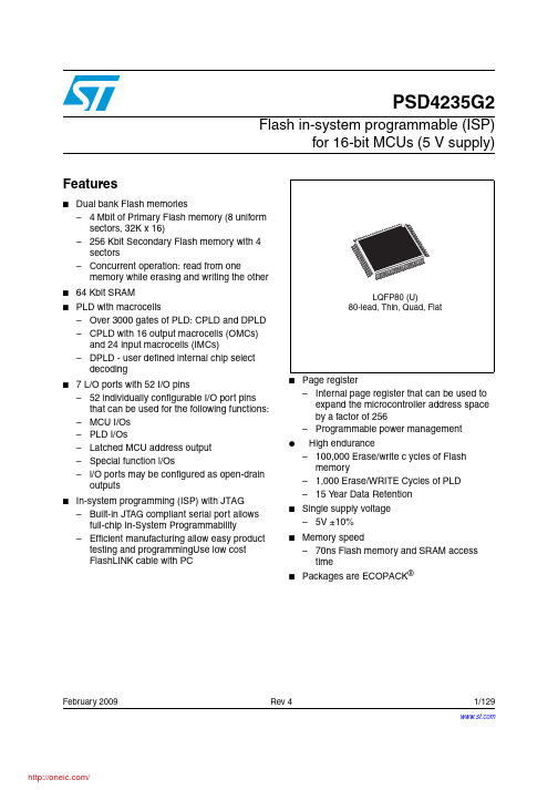
February 2009 Rev 41/129PSD4235G2Flash in-system programmable (ISP)for 16-bit MCUs (5 V supply)Features■Dual bank Flash memories– 4 Mbit of Primary Flash memory (8 uniform sectors, 32K x 16)–256 Kbit Secondary Flash memory with 4 sectors–Concurrent operation: read from onememory while erasing and writing the other ■64 Kbit SRAM■PLD with macrocells–Over 3000 gates of PLD: CPLD and DPLD –CPLD with 16 output macrocells (OMCs) and 24 input macrocells (IMCs)–DPLD - user defined internal chip select decoding ■7 L/O ports with 52 I/O pins–52 individually configurable I/O port pins that can be used for the following functions:–MCU I/Os –PLD I/Os–Latched MCU address output –Special function l/Os–l/O ports may be configured as open-drain outputs ■In-system programming (ISP) with JTAG –Built-in JTAG compliant serial port allows full-chip In-System Programmability–Efficient manufacturing allow easy product testing and programmingUse low cost FlashLINK cable with PC■Page register–Internal page register that can be used to expand the microcontroller address space by a factor of 256–Programmable power management ●High endurance–100,000 Erase/write c ycles of Flash memory–1,000 Erase/WRITE Cycles of PLD –15 Y ear Data Retention ■Single supply voltage –5V ±10%■Memory speed–70ns Flash memory and SRAM access time ■Packages are ECOPACK ®Contents PSD4235G2Contents1Summary description . . . . . . . . . . . . . . . . . . . . . . . . . . . . . . . . . . . . . . . 121.1In-system programming (ISP) via JTAG . . . . . . . . . . . . . . . . . . . . . . . . . . 121.1.1First time programming . . . . . . . . . . . . . . . . . . . . . . . . . . . . . . . . . . . . . 121.1.2Inventory build-up of pre-programmed devices . . . . . . . . . . . . . . . . . . . 121.1.3Expensive sockets . . . . . . . . . . . . . . . . . . . . . . . . . . . . . . . . . . . . . . . . . 121.2In-application programming (IAP) . . . . . . . . . . . . . . . . . . . . . . . . . . . . . . . 121.2.1Simultaneous READ and WRITE to Flash memory . . . . . . . . . . . . . . . . 131.2.2Complex memory mapping . . . . . . . . . . . . . . . . . . . . . . . . . . . . . . . . . . 131.2.3Separate Program and Data space . . . . . . . . . . . . . . . . . . . . . . . . . . . . 131.3PSDsoft™ Express . . . . . . . . . . . . . . . . . . . . . . . . . . . . . . . . . . . . . . . . . . 13 2Pin description . . . . . . . . . . . . . . . . . . . . . . . . . . . . . . . . . . . . . . . . . . . . 163PSD architectural overview . . . . . . . . . . . . . . . . . . . . . . . . . . . . . . . . . . 213.1Memory . . . . . . . . . . . . . . . . . . . . . . . . . . . . . . . . . . . . . . . . . . . . . . . . . . 213.2PLDs . . . . . . . . . . . . . . . . . . . . . . . . . . . . . . . . . . . . . . . . . . . . . . . . . . . . 213.3I/O ports . . . . . . . . . . . . . . . . . . . . . . . . . . . . . . . . . . . . . . . . . . . . . . . . . . 213.4MCU bus interface . . . . . . . . . . . . . . . . . . . . . . . . . . . . . . . . . . . . . . . . . . 223.5ISP via JTAG port . . . . . . . . . . . . . . . . . . . . . . . . . . . . . . . . . . . . . . . . . . . 223.6In-System Programming (ISP) . . . . . . . . . . . . . . . . . . . . . . . . . . . . . . . . . 223.7In-application programming (IAP) . . . . . . . . . . . . . . . . . . . . . . . . . . . . . . . 223.8Page register . . . . . . . . . . . . . . . . . . . . . . . . . . . . . . . . . . . . . . . . . . . . . . 223.9Power management unit (PMU) . . . . . . . . . . . . . . . . . . . . . . . . . . . . . . . . 23 4Development system . . . . . . . . . . . . . . . . . . . . . . . . . . . . . . . . . . . . . . . 24 5PSD register description and address offsets . . . . . . . . . . . . . . . . . . . 266Register bit definition . . . . . . . . . . . . . . . . . . . . . . . . . . . . . . . . . . . . . . . 286.1Data-In registers - port A, B, C, D, E, F, G . . . . . . . . . . . . . . . . . . . . . . . . 286.2Data-out registers - port A, B, C, D, E, F, G . . . . . . . . . . . . . . . . . . . . . . . 286.3Direction registers - ports A, B, C, D, E, F, G . . . . . . . . . . . . . . . . . . . . . . 286.4Control registers . . . . . . . . . . . . . . . . . . . . . . . . . . . . . . . . . . . . . . . . . . . . 28 2/129PSD4235G2Contents6.5Drive registers - Ports A, B, D, E, G . . . . . . . . . . . . . . . . . . . . . . . . . . . . . 296.6Drive registers - Ports C and F . . . . . . . . . . . . . . . . . . . . . . . . . . . . . . . . . 296.7Enable-Out registers - Ports A, B, C, F . . . . . . . . . . . . . . . . . . . . . . . . . . 296.8Input macrocells registers- ports A, B, C . . . . . . . . . . . . . . . . . . . . . . . . . 296.9Output macrocells A/B registers . . . . . . . . . . . . . . . . . . . . . . . . . . . . . . . . 306.10Mask macrocells A/B registers . . . . . . . . . . . . . . . . . . . . . . . . . . . . . . . . . 306.11Flash Memory Protection register . . . . . . . . . . . . . . . . . . . . . . . . . . . . . . 306.12Flash Boot Protection register . . . . . . . . . . . . . . . . . . . . . . . . . . . . . . . . . 316.13JTAG Enable register . . . . . . . . . . . . . . . . . . . . . . . . . . . . . . . . . . . . . . . . 316.14Page register . . . . . . . . . . . . . . . . . . . . . . . . . . . . . . . . . . . . . . . . . . . . . . 316.15PMMR0 register . . . . . . . . . . . . . . . . . . . . . . . . . . . . . . . . . . . . . . . . . . . . 316.16PMMR2 register . . . . . . . . . . . . . . . . . . . . . . . . . . . . . . . . . . . . . . . . . . . . 326.17VM register . . . . . . . . . . . . . . . . . . . . . . . . . . . . . . . . . . . . . . . . . . . . . . . . 336.18Memory_ID0 registers . . . . . . . . . . . . . . . . . . . . . . . . . . . . . . . . . . . . . . . 346.19Memory_ID1 register . . . . . . . . . . . . . . . . . . . . . . . . . . . . . . . . . . . . . . . . 347Detailed operation . . . . . . . . . . . . . . . . . . . . . . . . . . . . . . . . . . . . . . . . . . 357.1Memory blocks . . . . . . . . . . . . . . . . . . . . . . . . . . . . . . . . . . . . . . . . . . . . . 357.2Primary Flash memory and Secondary Flash memory description . . . . . 367.2.1Memory block Select signals . . . . . . . . . . . . . . . . . . . . . . . . . . . . . . . . . 367.2.2Ready/Busy (PE4) . . . . . . . . . . . . . . . . . . . . . . . . . . . . . . . . . . . . . . . . . 367.3Memory operation . . . . . . . . . . . . . . . . . . . . . . . . . . . . . . . . . . . . . . . . . . 368Instructions . . . . . . . . . . . . . . . . . . . . . . . . . . . . . . . . . . . . . . . . . . . . . . . 398.1Power-up condition . . . . . . . . . . . . . . . . . . . . . . . . . . . . . . . . . . . . . . . . . . 398.2Reading Flash memory . . . . . . . . . . . . . . . . . . . . . . . . . . . . . . . . . . . . . . 408.3Read memory contents . . . . . . . . . . . . . . . . . . . . . . . . . . . . . . . . . . . . . . 408.4Read Primary Flash identifier . . . . . . . . . . . . . . . . . . . . . . . . . . . . . . . . . . 408.5Read Memory Sector Protection status . . . . . . . . . . . . . . . . . . . . . . . . . . 408.6Reading the Erase/Program status bits . . . . . . . . . . . . . . . . . . . . . . . . . . 408.7Data Polling (DQ7) - DQ15 for Motorola . . . . . . . . . . . . . . . . . . . . . . . . . . 418.8Toggle flag (DQ6) - DQ14 for Motorola . . . . . . . . . . . . . . . . . . . . . . . . . . 418.9Error flag (DQ5) - DQ13 for Motorola . . . . . . . . . . . . . . . . . . . . . . . . . . . . 428.10Erase timeout flag (DQ3) - DQ11 for Motorola . . . . . . . . . . . . . . . . . . . . . 423/129Contents PSD4235G29Programming Flash memory . . . . . . . . . . . . . . . . . . . . . . . . . . . . . . . . . 439.1Data polling . . . . . . . . . . . . . . . . . . . . . . . . . . . . . . . . . . . . . . . . . . . . . . . 439.2Data toggle . . . . . . . . . . . . . . . . . . . . . . . . . . . . . . . . . . . . . . . . . . . . . . . . 449.3Unlock Bypass . . . . . . . . . . . . . . . . . . . . . . . . . . . . . . . . . . . . . . . . . . . . . 4510Erasing Flash memory . . . . . . . . . . . . . . . . . . . . . . . . . . . . . . . . . . . . . . 4710.1Flash Bulk Erase . . . . . . . . . . . . . . . . . . . . . . . . . . . . . . . . . . . . . . . . . . . 4710.2Suspend Sector Erase . . . . . . . . . . . . . . . . . . . . . . . . . . . . . . . . . . . . . . . 4810.3Resume Sector Erase . . . . . . . . . . . . . . . . . . . . . . . . . . . . . . . . . . . . . . . 4811Specific features . . . . . . . . . . . . . . . . . . . . . . . . . . . . . . . . . . . . . . . . . . . 4911.1Flash Memory Sector Protect . . . . . . . . . . . . . . . . . . . . . . . . . . . . . . . . . . 4911.2Reset . . . . . . . . . . . . . . . . . . . . . . . . . . . . . . . . . . . . . . . . . . . . . . . . . . . . 4911.3Reset (RESET) pin . . . . . . . . . . . . . . . . . . . . . . . . . . . . . . . . . . . . . . . . . . 49 12SRAM . . . . . . . . . . . . . . . . . . . . . . . . . . . . . . . . . . . . . . . . . . . . . . . . . . . . 5013Memory Select signals . . . . . . . . . . . . . . . . . . . . . . . . . . . . . . . . . . . . . . 5113.1Example . . . . . . . . . . . . . . . . . . . . . . . . . . . . . . . . . . . . . . . . . . . . . . . . . . 5113.2Memory Select configuration for MCUs with separateProgram and Data spaces . . . . . . . . . . . . . . . . . . . . . . . . . . . . . . . . . . . . 5113.3Separate space modes . . . . . . . . . . . . . . . . . . . . . . . . . . . . . . . . . . . . . . 5213.4Combined space modes . . . . . . . . . . . . . . . . . . . . . . . . . . . . . . . . . . . . . . 5213.580C51XA memory map example . . . . . . . . . . . . . . . . . . . . . . . . . . . . . . . 53 14Page register . . . . . . . . . . . . . . . . . . . . . . . . . . . . . . . . . . . . . . . . . . . . . . 54 15Memory ID registers . . . . . . . . . . . . . . . . . . . . . . . . . . . . . . . . . . . . . . . . 55 16PLDS . . . . . . . . . . . . . . . . . . . . . . . . . . . . . . . . . . . . . . . . . . . . . . . . . . . . . 56 17Decode PLD (DPLD) . . . . . . . . . . . . . . . . . . . . . . . . . . . . . . . . . . . . . . . . 5918Complex PLD (CPLD) . . . . . . . . . . . . . . . . . . . . . . . . . . . . . . . . . . . . . . . 6118.1Output macrocell (OMC) . . . . . . . . . . . . . . . . . . . . . . . . . . . . . . . . . . . . . 6218.2Product Term Allocator . . . . . . . . . . . . . . . . . . . . . . . . . . . . . . . . . . . . . . . 63 4/129PSD4235G2Contents18.3Loading and Reading the output macrocells (OMC) . . . . . . . . . . . . . . . . 6418.4The OMC Mask register . . . . . . . . . . . . . . . . . . . . . . . . . . . . . . . . . . . . . . 6418.5The output Enable of the OMC . . . . . . . . . . . . . . . . . . . . . . . . . . . . . . . . . 6418.6Input macrocells (IMC) . . . . . . . . . . . . . . . . . . . . . . . . . . . . . . . . . . . . . . . 6518.7External Chip Select . . . . . . . . . . . . . . . . . . . . . . . . . . . . . . . . . . . . . . . . . 6719MCU bus interface . . . . . . . . . . . . . . . . . . . . . . . . . . . . . . . . . . . . . . . . . . 6919.1PSD interface to a multiplexed bus . . . . . . . . . . . . . . . . . . . . . . . . . . . . . . 7019.2PSD interface to a non-multiplexed 8-bit bus . . . . . . . . . . . . . . . . . . . . . . 7119.3Data Byte Enable reference . . . . . . . . . . . . . . . . . . . . . . . . . . . . . . . . . . . 7119.4MCU bus interface examples . . . . . . . . . . . . . . . . . . . . . . . . . . . . . . . . . . 7219.580C196 and 80C186 . . . . . . . . . . . . . . . . . . . . . . . . . . . . . . . . . . . . . . . . 7319.6MC683xx and MC68HC16 . . . . . . . . . . . . . . . . . . . . . . . . . . . . . . . . . . . . 7419.780C51XA . . . . . . . . . . . . . . . . . . . . . . . . . . . . . . . . . . . . . . . . . . . . . . . . . 7519.8H8/300 . . . . . . . . . . . . . . . . . . . . . . . . . . . . . . . . . . . . . . . . . . . . . . . . . . . 7619.9MMC2001 . . . . . . . . . . . . . . . . . . . . . . . . . . . . . . . . . . . . . . . . . . . . . . . . . 7719.10C16x family . . . . . . . . . . . . . . . . . . . . . . . . . . . . . . . . . . . . . . . . . . . . . . . . 7720I/O ports . . . . . . . . . . . . . . . . . . . . . . . . . . . . . . . . . . . . . . . . . . . . . . . . . . 8020.1General port architecture . . . . . . . . . . . . . . . . . . . . . . . . . . . . . . . . . . . . . 8020.2Port operating modes . . . . . . . . . . . . . . . . . . . . . . . . . . . . . . . . . . . . . . . . 8120.3MCU I/O mode . . . . . . . . . . . . . . . . . . . . . . . . . . . . . . . . . . . . . . . . . . . . . 8220.4PLD I/O mode . . . . . . . . . . . . . . . . . . . . . . . . . . . . . . . . . . . . . . . . . . . . . . 8220.5Address Out mode . . . . . . . . . . . . . . . . . . . . . . . . . . . . . . . . . . . . . . . . . . 8220.6Address In mode . . . . . . . . . . . . . . . . . . . . . . . . . . . . . . . . . . . . . . . . . . . 8420.7Data Port mode . . . . . . . . . . . . . . . . . . . . . . . . . . . . . . . . . . . . . . . . . . . . 8420.8Peripheral I/O mode . . . . . . . . . . . . . . . . . . . . . . . . . . . . . . . . . . . . . . . . . 8420.9JTAG in-system programming (ISP) . . . . . . . . . . . . . . . . . . . . . . . . . . . . . 8520.10MCU Reset mode . . . . . . . . . . . . . . . . . . . . . . . . . . . . . . . . . . . . . . . . . . . 8520.11Port Configuration registers (PCR) . . . . . . . . . . . . . . . . . . . . . . . . . . . . . . 8620.12Control register . . . . . . . . . . . . . . . . . . . . . . . . . . . . . . . . . . . . . . . . . . . . . 8620.13Direction register . . . . . . . . . . . . . . . . . . . . . . . . . . . . . . . . . . . . . . . . . . . 8620.14Port Data registers . . . . . . . . . . . . . . . . . . . . . . . . . . . . . . . . . . . . . . . . . . 8820.15Data In . . . . . . . . . . . . . . . . . . . . . . . . . . . . . . . . . . . . . . . . . . . . . . . . . . . 885/129Contents PSD4235G26/12920.16Data Out register . . . . . . . . . . . . . . . . . . . . . . . . . . . . . . . . . . . . . . . . . . . 88 20.17Output macrocells (OMC) . . . . . . . . . . . . . . . . . . . . . . . . . . . . . . . . . . . . . 88 20.18Mask macrocell register . . . . . . . . . . . . . . . . . . . . . . . . . . . . . . . . . . . . . . 88 20.19Input macrocells (IMC) . . . . . . . . . . . . . . . . . . . . . . . . . . . . . . . . . . . . . . . 88 20.20Enable Out . . . . . . . . . . . . . . . . . . . . . . . . . . . . . . . . . . . . . . . . . . . . . . . . 89 20.21Ports A, B and C - functionality and structure . . . . . . . . . . . . . . . . . . . . . 89 20.22Port D - functionality and structure . . . . . . . . . . . . . . . . . . . . . . . . . . . . . . 90 20.23Port E - functionality and structure . . . . . . . . . . . . . . . . . . . . . . . . . . . . . . 91 20.24Port F - functionality and structure . . . . . . . . . . . . . . . . . . . . . . . . . . . . . . 92 20.25Port G - functionality and structure . . . . . . . . . . . . . . . . . . . . . . . . . . . . . . 9221Power management . . . . . . . . . . . . . . . . . . . . . . . . . . . . . . . . . . . . . . . . . 9421.1Automatic Power-down (APD) Unit and Power-down mode . . . . . . . . . . . 9521.2Power-down mode . . . . . . . . . . . . . . . . . . . . . . . . . . . . . . . . . . . . . . . . . . 9521.3Other power saving options . . . . . . . . . . . . . . . . . . . . . . . . . . . . . . . . . . . 9621.4PLD power management . . . . . . . . . . . . . . . . . . . . . . . . . . . . . . . . . . . . . 9621.5PSD Chip Select input (CSI, PD2) . . . . . . . . . . . . . . . . . . . . . . . . . . . . . . 9721.6Input clock . . . . . . . . . . . . . . . . . . . . . . . . . . . . . . . . . . . . . . . . . . . . . . . . 9721.7Input control signals . . . . . . . . . . . . . . . . . . . . . . . . . . . . . . . . . . . . . . . . . 9822Power-on Reset, Warm Reset and Power-down . . . . . . . . . . . . . . . . . . 9922.1Power-on Reset . . . . . . . . . . . . . . . . . . . . . . . . . . . . . . . . . . . . . . . . . . . . 9922.2Warm Reset . . . . . . . . . . . . . . . . . . . . . . . . . . . . . . . . . . . . . . . . . . . . . . . 9922.3I/O pin, register and PLD status at Reset . . . . . . . . . . . . . . . . . . . . . . . . . 9922.4Reset of Flash Memory Erase and Program cycles . . . . . . . . . . . . . . . . . 9923Programming in-circuit using the JTAG serial interface . . . . . . . . . . 10123.1Standard JTAG signals . . . . . . . . . . . . . . . . . . . . . . . . . . . . . . . . . . . . . . 10123.2JTAG extensions . . . . . . . . . . . . . . . . . . . . . . . . . . . . . . . . . . . . . . . . . . . 10223.3Security and Flash memory protection . . . . . . . . . . . . . . . . . . . . . . . . . . 102 24Initial delivery state . . . . . . . . . . . . . . . . . . . . . . . . . . . . . . . . . . . . . . . . 104 25Maximum rating . . . . . . . . . . . . . . . . . . . . . . . . . . . . . . . . . . . . . . . . . . . 105PSD4235G2Contents 26DC and AC parameters . . . . . . . . . . . . . . . . . . . . . . . . . . . . . . . . . . . . . 106 27Package mechanical . . . . . . . . . . . . . . . . . . . . . . . . . . . . . . . . . . . . . . . 124 28Part numbering . . . . . . . . . . . . . . . . . . . . . . . . . . . . . . . . . . . . . . . . . . . 126 Appendix A Pin assignments . . . . . . . . . . . . . . . . . . . . . . . . . . . . . . . . . . . . . . . 127 29Revision history . . . . . . . . . . . . . . . . . . . . . . . . . . . . . . . . . . . . . . . . . . 1287/129List of tables PSD4235G2 List of tablesTable 1.Pin names. . . . . . . . . . . . . . . . . . . . . . . . . . . . . . . . . . . . . . . . . . . . . . . . . . . . . . . . . . . . . . 14 Table 2.Pin description (for the LQFP package) . . . . . . . . . . . . . . . . . . . . . . . . . . . . . . . . . . . . . . . 16 Table 3.PLD I/O. . . . . . . . . . . . . . . . . . . . . . . . . . . . . . . . . . . . . . . . . . . . . . . . . . . . . . . . . . . . . . . . 22 Table 4.JTAG signals on port E. . . . . . . . . . . . . . . . . . . . . . . . . . . . . . . . . . . . . . . . . . . . . . . . . . . . 22 Table 5.Methods of programming different functional blocks of the PSD . . . . . . . . . . . . . . . . . . . . 23 Table 6.Register address offset. . . . . . . . . . . . . . . . . . . . . . . . . . . . . . . . . . . . . . . . . . . . . . . . . . . . 26 Table 7.Data-In registers - Ports A, B, C, D, E, F, G. . . . . . . . . . . . . . . . . . . . . . . . . . . . . . . . . . . . 28 Table 8.Data-Out registers - Ports A, B, C, D, E, F, G . . . . . . . . . . . . . . . . . . . . . . . . . . . . . . . . . . 28 Table 9.Direction registers - Ports A, B, C, D, E, F, G. . . . . . . . . . . . . . . . . . . . . . . . . . . . . . . . . . . 28 Table 10.Control registers - Ports E, F, G. . . . . . . . . . . . . . . . . . . . . . . . . . . . . . . . . . . . . . . . . . . . . 28 Table 11.Drive registers - Ports A, B, D, E, G. . . . . . . . . . . . . . . . . . . . . . . . . . . . . . . . . . . . . . . . . . 29 Table 12.Drive registers - Ports C, F. . . . . . . . . . . . . . . . . . . . . . . . . . . . . . . . . . . . . . . . . . . . . . . . . 29 Table 13.Enable-Out registers - Ports A, B, C, F. . . . . . . . . . . . . . . . . . . . . . . . . . . . . . . . . . . . . . . . 29 Table 14.Input macrocell registers - Port A, B, C . . . . . . . . . . . . . . . . . . . . . . . . . . . . . . . . . . . . . . . 29 Table 15.Output macrocells A register . . . . . . . . . . . . . . . . . . . . . . . . . . . . . . . . . . . . . . . . . . . . . . . 30 Table 16.Output macrocells B register . . . . . . . . . . . . . . . . . . . . . . . . . . . . . . . . . . . . . . . . . . . . . . . 30 Table 17.Mask macrocells A register. . . . . . . . . . . . . . . . . . . . . . . . . . . . . . . . . . . . . . . . . . . . . . . . . 30 Table 18.Mask macrocells B register. . . . . . . . . . . . . . . . . . . . . . . . . . . . . . . . . . . . . . . . . . . . . . . . . 30 Table 19.Flash Memory Protection register. . . . . . . . . . . . . . . . . . . . . . . . . . . . . . . . . . . . . . . . . . . . 30 Table 20.Flash Boot Protection register . . . . . . . . . . . . . . . . . . . . . . . . . . . . . . . . . . . . . . . . . . . . . . 31 Table 21.JTAG Enable register. . . . . . . . . . . . . . . . . . . . . . . . . . . . . . . . . . . . . . . . . . . . . . . . . . . . . 31 Table 22.Page register . . . . . . . . . . . . . . . . . . . . . . . . . . . . . . . . . . . . . . . . . . . . . . . . . . . . . . . . . . . 31 Table 23.PMMR0 register . . . . . . . . . . . . . . . . . . . . . . . . . . . . . . . . . . . . . . . . . . . . . . . . . . . . . . . . . 31 Table 24.PMMR2 register . . . . . . . . . . . . . . . . . . . . . . . . . . . . . . . . . . . . . . . . . . . . . . . . . . . . . . . . . 32 Table 25.VM register. . . . . . . . . . . . . . . . . . . . . . . . . . . . . . . . . . . . . . . . . . . . . . . . . . . . . . . . . . . . . 33 Table 26.Memory_ID0 register . . . . . . . . . . . . . . . . . . . . . . . . . . . . . . . . . . . . . . . . . . . . . . . . . . . . . 34 Table 27.Memory_ID1 register . . . . . . . . . . . . . . . . . . . . . . . . . . . . . . . . . . . . . . . . . . . . . . . . . . . . . 34 Table 28.Memory block size and organization . . . . . . . . . . . . . . . . . . . . . . . . . . . . . . . . . . . . . . . . . 35 Table 29.Instructions. . . . . . . . . . . . . . . . . . . . . . . . . . . . . . . . . . . . . . . . . . . . . . . . . . . . . . . . . . . . . 37 Table 30.Status bits. . . . . . . . . . . . . . . . . . . . . . . . . . . . . . . . . . . . . . . . . . . . . . . . . . . . . . . . . . . . . . 41 Table 31.Status bits for Motorola. . . . . . . . . . . . . . . . . . . . . . . . . . . . . . . . . . . . . . . . . . . . . . . . . . . . 41 Table 32.DPLD and CPLD inputs . . . . . . . . . . . . . . . . . . . . . . . . . . . . . . . . . . . . . . . . . . . . . . . . . . . 56 Table 33.Output macrocell Port and Data bit Assignments. . . . . . . . . . . . . . . . . . . . . . . . . . . . . . . . 63 Table 34.MCUs and their control signals. . . . . . . . . . . . . . . . . . . . . . . . . . . . . . . . . . . . . . . . . . . . . . 69 Table 35.16-bit data bus with BHE . . . . . . . . . . . . . . . . . . . . . . . . . . . . . . . . . . . . . . . . . . . . . . . . . . 71 Table 36.16-bit data bus with WRH and WRL. . . . . . . . . . . . . . . . . . . . . . . . . . . . . . . . . . . . . . . . . . 72 Table 37.16-bit data bus with SIZ0, A0 (Motorola MCU). . . . . . . . . . . . . . . . . . . . . . . . . . . . . . . . . . 72 Table 38.16-bit data bus with LDS, UDS (Motorola MCU). . . . . . . . . . . . . . . . . . . . . . . . . . . . . . . . . 72 Table 39.Port operating modes. . . . . . . . . . . . . . . . . . . . . . . . . . . . . . . . . . . . . . . . . . . . . . . . . . . . . 82 Table 40.Port operating mode settings . . . . . . . . . . . . . . . . . . . . . . . . . . . . . . . . . . . . . . . . . . . . . . . 83 Table 41.I/O port latched address output assignments. . . . . . . . . . . . . . . . . . . . . . . . . . . . . . . . . . . 84 Table 42.Port Configuration registers (PCR). . . . . . . . . . . . . . . . . . . . . . . . . . . . . . . . . . . . . . . . . . . 86 Table 43.Port Pin Direction Control, output Enable P.T. not defined. . . . . . . . . . . . . . . . . . . . . . . . . 87 Table 44.Port Pin Direction Control, output Enable P.T. defined. . . . . . . . . . . . . . . . . . . . . . . . . . . . 87 Table 45.Port direction assignment example. . . . . . . . . . . . . . . . . . . . . . . . . . . . . . . . . . . . . . . . . . . 87 Table 46.Drive register pin assignment. . . . . . . . . . . . . . . . . . . . . . . . . . . . . . . . . . . . . . . . . . . . . . . 87 Table 47.Port Data registers . . . . . . . . . . . . . . . . . . . . . . . . . . . . . . . . . . . . . . . . . . . . . . . . . . . . . . . 88 Table 48.Effect of Power-down mode on ports . . . . . . . . . . . . . . . . . . . . . . . . . . . . . . . . . . . . . . . . . 95 8/129PSD4235G2List of tables Table 49.PSD timing and standby current during Power-down mode. . . . . . . . . . . . . . . . . . . . . . . . 96 Table 50.APD counter operation. . . . . . . . . . . . . . . . . . . . . . . . . . . . . . . . . . . . . . . . . . . . . . . . . . . . 98 Table 51.Status During Power-On Reset, Warm Reset and Power-down mode. . . . . . . . . . . . . . . . 99 Table 52.JTAG port signals. . . . . . . . . . . . . . . . . . . . . . . . . . . . . . . . . . . . . . . . . . . . . . . . . . . . . . . 102 Table 53.Absolute maximum ratings. . . . . . . . . . . . . . . . . . . . . . . . . . . . . . . . . . . . . . . . . . . . . . . . 105 Table 54.Example of PSD typical power calculation at V CC = 5.0V (with Turbo mode on). . . . . . . 107 Table 55.Example of PSD typical power calculation at V CC = 5.0V (with Turbo mode off). . . . . . . 108 Table 56.Operating conditions. . . . . . . . . . . . . . . . . . . . . . . . . . . . . . . . . . . . . . . . . . . . . . . . . . . . . 109 Table 57.AC signal letters for PLD timings . . . . . . . . . . . . . . . . . . . . . . . . . . . . . . . . . . . . . . . . . . . 109 Table 58.AC signal behavior symbols for PLD timings . . . . . . . . . . . . . . . . . . . . . . . . . . . . . . . . . . 109 Table 59.AC measurement conditions. . . . . . . . . . . . . . . . . . . . . . . . . . . . . . . . . . . . . . . . . . . . . . . 110 Table 60.Capacitance . . . . . . . . . . . . . . . . . . . . . . . . . . . . . . . . . . . . . . . . . . . . . . . . . . . . . . . . . . . 110 Table 61.DC characteristics. . . . . . . . . . . . . . . . . . . . . . . . . . . . . . . . . . . . . . . . . . . . . . . . . . . . . . . 111 Table 62.CPLD Combinatorial timing . . . . . . . . . . . . . . . . . . . . . . . . . . . . . . . . . . . . . . . . . . . . . . . 112 Table 63.CPLD macrocell Synchronous clock mode timing . . . . . . . . . . . . . . . . . . . . . . . . . . . . . . 113 Table 64.CPLD macrocell Asynchronous clock mode timing . . . . . . . . . . . . . . . . . . . . . . . . . . . . . 114 Table 65.Input macrocell timing. . . . . . . . . . . . . . . . . . . . . . . . . . . . . . . . . . . . . . . . . . . . . . . . . . . . 115 Table 66.Program, WRITE and Erase times. . . . . . . . . . . . . . . . . . . . . . . . . . . . . . . . . . . . . . . . . . 116 Table 67.READ timing. . . . . . . . . . . . . . . . . . . . . . . . . . . . . . . . . . . . . . . . . . . . . . . . . . . . . . . . . . . 117 Table 68.WRITE timing . . . . . . . . . . . . . . . . . . . . . . . . . . . . . . . . . . . . . . . . . . . . . . . . . . . . . . . . . . 119 Table 69.Port F Peripheral Data Mode Read timing . . . . . . . . . . . . . . . . . . . . . . . . . . . . . . . . . . . . 121 Table 70.Port F Peripheral Data Mode Write timing . . . . . . . . . . . . . . . . . . . . . . . . . . . . . . . . . . . . 121 Table 71.Reset (RESET) timing . . . . . . . . . . . . . . . . . . . . . . . . . . . . . . . . . . . . . . . . . . . . . . . . . . . 121 Table 72.Power-down timing. . . . . . . . . . . . . . . . . . . . . . . . . . . . . . . . . . . . . . . . . . . . . . . . . . . . . . 122 Table 73.ISC timing. . . . . . . . . . . . . . . . . . . . . . . . . . . . . . . . . . . . . . . . . . . . . . . . . . . . . . . . . . . . . 123 Table 74.LQFP80 - 80-lead plastic thin, quad, flat package mechanical data. . . . . . . . . . . . . . . . . 124 Table 75.Ordering information scheme. . . . . . . . . . . . . . . . . . . . . . . . . . . . . . . . . . . . . . . . . . . . . . 126 Table 76.PSD4235G2 LQFP80. . . . . . . . . . . . . . . . . . . . . . . . . . . . . . . . . . . . . . . . . . . . . . . . . . . . 127 Table 77.Document revision history . . . . . . . . . . . . . . . . . . . . . . . . . . . . . . . . . . . . . . . . . . . . . . . . 1289/129。
2305;中文规格书,Datasheet资料
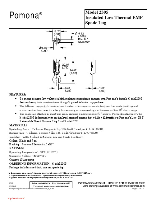
Pomona®All dimensions are in inches. Tolerances (except noted): .xx = ±.02” (,51 mm), .xxx = ± .005” (,127 mm).All specifications are to the latest revisions. Specifications are subject to change without notice.Registered trademarks are the property of their respective companies. Made in USA6/9/99Pomona ACCESS 90138 (800) 444-6785 or (425) 446-6010 SY/EH/LS More drawings available at Page 1 of 1 Model 2305 Insulated Low Thermal EMF Spade LugSales: 800-490-2361 Fax: 888-403-3360 Technical Assistance: 800-241-2060 FEATURES:• To ensure accurate low voltage or high resistance precision measurements, Pomona’s durable Model 2305features heavy duty construction with a gold plated tellurium copper base.• The tellurium copper/gold material combination offers superior conductivity and low oxide build-up andminimizes the thermoelectric effect, thus ensuring accurate readings in the nano-volt or 109 ohmic range.• The spade lug attaches to shunt terminals, standard binding posts or ¼” screws. For meter attachment, theModel 2305 is designed with an insulated standard banana jack which will interface to Pomona’s Low EMF Retractable Sheath Banana Plug Cord Model 5291.MATERIALS:Spade Lug Body – Tellurium Copper, Alloy 145, Gold Plated per MIL-G-45204Banana Jack – Tellurium Copper, Alloy 145, Gold Plated per MIL-G-45204Insulation – ABS Molded to Banana Jack and Spade Lug BodyColors: Black and Red, Marking: “Pomona Electronics, Calif.”RATINGS:Operating Temperature: +50°C (+122°F)Operating Voltage – 5000 VDCCurrent: 15 AmperesORDERING INFORMATION: Model 2305Package includes one black, one red spade lug/分销商库存信息: POMONA2305。
2N7002K,215;中文规格书,Datasheet资料

2N7002KTrenchMOS™ logic level FETRev. 01 — 20 October 2003Product dataM3D0881.Product profile1.1DescriptionN-channel enhancement mode field-effect transistor in a plastic package using TrenchMOS™ technology.1.2Features1.3Applications1.4Quick reference data2.Pinning informations Logic level compatible s Very fast switchings Subminiature surface mount package s Gate-source ESD protection diodes.s Relay drivers High speed line driver.s V DS ≤60V s I D ≤340mA s P tot ≤0.83Ws R DSon ≤3.9Ω.Table 1:Pinning - SOT23, simplified outline and symbolPin Description Simplified outlineSymbol1gate (g)SOT232source (s)3drain (d)MSB003Top view123gds03ab603.Ordering informationTable 2:Ordering informationType number PackageName Description Version2N7002K SOT23Plastic surface mounted package; 3 leads.SOT23 4.Limiting valuesTable 3:Limiting valuesIn accordance with the Absolute Maximum Rating System (IEC 60134).Symbol Parameter Conditions Min Max Unit V DS drain-source voltage (DC)25°C≤T j≤150°C-60VV DGR drain-gate voltage (DC)25°C≤T j≤150°C; R GS=20kΩ-60VV GS gate-source voltage (DC)-±15VI D drain current (DC)T sp=25°C; V GS=10V;Figure2and3-340mAT sp=100°C; V GS=10V;Figure2-215mA I DM peak drain current T sp=25°C; pulsed; t p≤10µs;Figure3-680mA P tot total power dissipation T sp=25°C;Figure1-0.83W T stg storage temperature−65+150°C T j junction temperature−65+150°C Source-drain diodeI S source (diode forward) current (DC)T sp=25°C-340mA I SM peak source (diode forward) current T sp=25°C; pulsed; t p≤10µs-680mA Electrostatic discharge voltageV esd electrostatic discharge voltage Human Body Model1; C=100pF; R=1.5kΩ-1kVFig 1.Normalized total power dissipation as afunction of solder point temperature.Fig 2.Normalized continuous drain current as afunction of solder point temperature.T sp =25°C; I DM is single pulse; V GS =10VFig 3.Safe operating area; continuous and peak drain currents as a function of drain-source voltage.03aa1704080120050100150200(%)T sp (°C)P der 03aa2504080120050100150200T sp (°C)I der (%)P der P totP tot 25C °()-----------------------100%×=I der I DI D 25C °()-------------------100%×=03an6610-210-11110102V DS (V)I D (A)DC100 ms10 msLimit R DSon = V DS / I D1 mst p = 10 µs100 µs5.Thermal characteristics5.1Transient thermal impedanceTable 4:Thermal characteristicsSymbol ParameterConditionsMin Typ Max Unit R th(j-sp)thermal resistance from junction to solder point Figure 4--150K/W R th(j-a)thermal resistance from junction to ambientminimum footprint;mounted on a printed-circuit board-350-K/WFig 4.Transient thermal impedance from junction to solder point as a function of pulse duration.03aa3911010210310-510-410-310-210-1110t p (s)Z th(j-sp)(K/W)single pulseδ = 0.50.20.10.050.02t pt p TPtTδ =6.CharacteristicsTable 5:CharacteristicsT j=25°C unless otherwise specified.Symbol Parameter Conditions Min Typ Max Unit Static characteristicsV(BR)DSS drain-source breakdown voltage I D=10µA; V GS=0VT j=25°C6075-VT j=−55°C55--VV(BR)GSS drain-source breakdown voltage I G=±1mA; V DS=0V1622-VV GS(th)gate-source threshold voltage I D=1mA; V DS=V GS;Figure9VT j=25°C12-VT j=150°C0.6--VT j=−55°C-- 3.5VI DSS drain-source leakage current V DS=48V; V GS=0VT j=25°C-0.011µAT j=150°C--10µA I GSS gate-source leakage current V GS=±10V; V DS=0V-50500nA R DSon drain-source on-state resistance V GS=10V; I D=500mA;Figure7and8T j=25°C- 2.8 3.9ΩT j=150°C- 5.27.2ΩV GS=4.5V; I D=200mA;Figure7and8- 3.8 5.3ΩDynamic characteristicsC iss input capacitance V GS=0V; V DS=10V; f=1MHz;Figure11-1340pFC oss output capacitance-830pF C rss reverse transfer capacitance-410pFt on turn-on time V DD=50V; R L=250Ω;V GS=10V;R G=50Ω; R GS=50Ω-310nst off turn-off time-915ns Source-drain diodeV SD source-drain (diode forward) voltage I S=300mA; V GS=0V;Figure12-0.93 1.5Vt rr reverse recovery time I S=300mA; dI S/dt=−100A/µs;V GS=0V; V R=25V -30-nsQ r recovered charge-30-nCT j =25°C T j =25°C and 150°C; V DS >I D x R DSonFig 5.Output characteristics: drain current as afunction of drain-source voltage;typical values.Fig 6.Transfer characteristics: drain current as afunction of gate-source voltage; typical values.T j =25°CFig 7.Drain-source on-state resistance as a functionof drain current; typical values.Fig 8.Normalized drain-source on-state resistance factor as a function of junction temperature.03an7000.10.20.30.40.500.511.52V DS (V)I D (A) 3.5 VT j = 25 °CV GS = 10V4 V4.5 V3 V6 V03an7200.10.20.30.40.50246V GS (V)I D (A)V DS > I D x R DSonT j = 25 °C150 °C03an71024681000.10.20.30.40.5I D (A)R DSon (Ω)V GS = 3.5 VT j = 25 °C4.5 V4 V10 V6 V 03aa2800.61.21.82.4-6060120180a T j (°C)a RDSon R DSon 25C °()----------------------------=I D =1mA; V DS =V GS T j =25°C; V DS =5VFig 9.Gate-source threshold voltage as a function ofjunction temperature.Fig 10.Sub-threshold drain current as a function ofgate-source voltage.V GS =0V; f =1MHzFig 11.Input, output and reverse transfer capacitances as a function of drain-source voltage; typical values.03aa3400.61.21.82.4-6060120180T j (°C)V GS(th)(V)typmin03aa3710-610-510-410-310-210-100.61.21.82.4V GS (V)I D (A)typmin03aa4611010210-11 10102V DS (V)C (pF)C issC ossC rssT j =25°C and 150°C; V GS =0V I D =0.5A; V DD =48VFig 12.Source (diode forward) current as a function ofsource-drain (diode forward) voltage; typical values.Fig 13.Gate-source voltage as a function of gatecharge; typical values.03an7300.10.20.30.40.500.30.60.91.2V SD (V)I S (A)T j = 25 °C150 °CV GS = 0 V03ab090510150.30.60.91.2Q G (nC)V GS (V)I D = 0.5AV DD = 48 V T j = 25 °C7.Package outlineFig 14.SOT23.UNIT A 1max.b p c D E e 1H E L p Q w v REFERENCESOUTLINE VERSION EUROPEAN PROJECTIONISSUE DATE 97-02-2899-09-13IECJEDEC EIAJmm0.10.480.380.150.093.02.81.41.20.95e 1.92.52.10.550.450.10.2DIMENSIONS (mm are the original dimensions)0.450.15SOT23TO-236ABb pD e 1eAA 1L pQdetail XH EE w M v M ABAB 01 2 mmscaleA 1.10.9cX123Plastic surface mounted package; 3 leadsSOT238.Revision historyTable 6:Revision historyRev Date CPCN Description0120031020Product data (9397 750 11703)分销商库存信息: NXP2N7002K,215。
W25Q128BVEIG;中文规格书,Datasheet资料

Publication Release Date: April 18, 20123V 128M-BITSERIAL FLASH MEMORY WITH DUAL AND QUAD SPITable of Contents1.GENERAL DESCRIPTION (5)2.FEATURES (5)3.PACKAGE TYPES AND PIN CONFIGURATIONS (6)3.1Pad Configuration WSON 8x6-mm (6)3.2Pad Description WSON 8x6-mm (6)3.3Pin Configuration SOIC 300-mil (7)3.4Pin Description SOIC 300-mil (7)3.5Ball Configuration TFBGA 8x6-mm (5x5 or 6x4 Ball Array) (8)3.6Ball Description TFBGA 8x6-mm (8)4.PIN DESCRIPTIONS (9)4.1Chip Select (/CS) (9)4.2Serial Data Input, Output and IOs (DI, DO and IO0, IO1, IO2, IO3) (9)4.3Write Protect (/WP) (9)4.4HOLD (/HOLD) (9)4.5Serial Clock (CLK) (9)5.BLOCK DIAGRAM (10)6.FUNCTIONAL DESCRIPTIONS (11)6.1SPI OPERATIONS (11)6.1.1Standard SPI Instructions (11)6.1.2Dual SPI Instructions (11)6.1.3Quad SPI Instructions (11)6.1.4Hold Function (11)6.2WRITE PROTECTION (12)6.2.1Write Protect Features (12)7.STATUS REGISTERS AND INSTRUCTIONS (13)7.1STATUS REGISTERS (13)7.1.1BUSY Status (BUSY) (13)7.1.2Write Enable Latch Status (WEL) (13)7.1.3Block Protect Bits (BP2, BP1, BP0) (13)7.1.4Top/Bottom Block Protect Bit (TB) (13)7.1.5Sector/Block Protect Bit (SEC) (13)7.1.6Complement Protect Bit (CMP) (14)7.1.7Status Register Protect Bits (SRP1, SRP0) (14)7.1.8Erase/Program Suspend Status (SUS) (14)7.1.9Security Register Lock Bits (LB3, LB2, LB1) (14)7.1.10Quad Enable Bit (QE) (15)7.1.11Status Register Memory Protection (CMP = 0) (16)7.1.12 Status Register Memory Protection (CMP = 1) (17)Publication Release Date: April 18, 20127.2 INSTRUCTIONS (18)7.2.1 Manufacturer and Device Identification ................................................................................ 18 7.2.2 Instruction Set Table 1 (Erase, Program Instructions) .......................................................... 19 7.2.3 Instruction Set Table 2 (Read Instructions) .......................................................................... 20 7.2.4 Instruction Set Table 3 (ID, Security Instructions) ................................................................ 21 7.2.5 Write Enable (06h) ............................................................................................................... 22 7.2.6 Write Enable for Volatile Status Register (50h) .................................................................... 22 7.2.7 Write Disable (04h) ............................................................................................................... 23 7.2.8 Read Status Register-1 (05h) and Read Status Register-2 (35h) ........................................ 24 7.2.9 Write Status Register (01h) .................................................................................................. 24 7.2.10 Read Data (03h) ................................................................................................................. 26 7.2.11 Fast Read (0Bh) ................................................................................................................. 27 7.2.12 Fast Read Dual Output (3Bh) ............................................................................................. 28 7.2.13 Fast Read Quad Output (6Bh) ............................................................................................ 29 7.2.14 Fast Read Dual I/O (BBh) ................................................................................................... 30 7.2.15 Fast Read Quad I/O (EBh) ................................................................................................. 32 7.2.16 Word Read Quad I/O (E7h) ................................................................................................ 34 7.2.17 Octal Word Read Quad I/O (E3h) ....................................................................................... 36 7.2.18 Set Burst with Wrap (77h) .................................................................................................. 38 7.2.19 Continuous Read Mode Bits (M7-0) ................................................................................... 39 7.2.20 Continuous Read Mode Reset (FFh or FFFFh) .................................................................. 39 7.2.21 Page Program (02h) ........................................................................................................... 40 7.2.22 Quad Input Page Program (32h) ........................................................................................ 41 7.2.23 Sector Erase (20h) ............................................................................................................. 42 7.2.24 32KB Block Erase (52h) ..................................................................................................... 43 7.2.25 64KB Block Erase (D8h) ..................................................................................................... 44 7.2.26 Chip Erase (C7h / 60h) ....................................................................................................... 45 7.2.27 Erase / Program Suspend (75h) ......................................................................................... 46 7.2.28 Erase / Program Resume (7Ah) ......................................................................................... 47 7.2.29 Power-down (B9h) .............................................................................................................. 48 7.2.30 Release Power-down / Device ID (ABh) ............................................................................. 49 7.2.31 Read Manufacturer / Device ID (90h) ................................................................................. 51 7.2.32 Read Manufacturer / Device ID Dual I/O (92h) ................................................................... 52 7.2.33 Read Manufacturer / Device ID Quad I/O (94h) ................................................................. 53 7.2.34 Read Unique ID Number (4Bh)........................................................................................... 54 7.2.35 Read JEDEC ID (9Fh) ........................................................................................................ 55 7.2.36 Read SFDP Register (5Ah) ................................................................................................ 56 7.2.37 Erase Security Registers (44h) ........................................................................................... 57 7.2.38 Program Security Registers (42h) ...................................................................................... 58 7.2.39 Read Security Registers (48h) . (59)8.ELECTRICAL CHARACTERISTICS (60)8.1Absolute Maximum Ratings (60)8.2Operating Ranges (60)8.3Power-up Timing and Write Inhibit Threshold (61)8.4DC Electrical Characteristics (62)8.5AC Measurement Conditions (63)8.6AC Electrical Characteristics (64)8.7AC Electrical Characteristics (cont’d) (65)8.8Serial Output Timing (66)8.9Serial Input Timing (66)8.10HOLD Timing (66)8.11WP Timing (66)9.PACKAGE SPECIFICATION (67)9.18-Pad WSON 8x6-mm (Package Code E) (67)9.216-Pin SOIC 300-mil (Package Code F) (68)9.324-Ball TFBGA 8x6-mm (Package Code B, 5x5-1 Ball Array) (69)9.424-Ball TFBGA 8x6-mm (Package Code C, 6x4 Ball Array) (70)10.ORDERING INFORMATION (71)10.1Valid Part Numbers and Top Side Marking (72)11.REVISION HISTORY (73)Publication Release Date: April 18, 20121. GENERAL DESCRIPTIONThe W25Q128BV (128M-bit) Serial Flash memory provides a storage solution for systems with limited space, pins and power. The 25Q series offers flexibility and performance well beyond ordinary Serial Flash devices. They are ideal for code shadowing to RAM, executing code directly from Dual/Quad SPI (XIP) and storing voice, text and data. The device operates on a single 2.7V to 3.6V power supply with current consumption as low as 4mA active and 1µA for power-down.The W25Q128BV array is organized into 65,536 programmable pages of 256-bytes each. Up to 256 bytes can be programmed at a time. Pages can be erased in groups of 16 (4KB sector erase), groups of 128 (32KB block erase), groups of 256 (64KB block erase) or the entire chip (chip erase). The W25Q128BV has 4,096 erasable sectors and 256 erasable blocks respectively. The small 4KB sectors allow for greater flexibility in applications that require data and parameter storage. (See Figure 2.)The W25Q128BV supports the standard Serial Peripheral Interface (SPI), and a high performance Dual/Quad output as well as Dual/Quad I/O SPI: Serial Clock, Chip Select, Serial Data I/O0 (DI), I/O1 (DO), I/O2 (/WP), and I/O3 (/HOLD). SPI clock frequencies of up to 104MHz are supported allowing equivalent clock rates of 208MHz (104MHz x 2) for Dual Output and 280MHz (70MHz x 4) for Quad SPI when using the Fast Read Quad SPI instructions. These transfer rates can outperform standard Asynchronous 8 and 16-bit Parallel Flash memories. The Continuous Read Mode allows for efficient memory access with as few as 8-clocks of instruction-overhead to read a 24-bit address, allowing true XIP (execute in place) operation.A Hold pin, Write Protect pin and programmable write protection, with top, bottom or complement array control, provide further control flexibility. Additionally, the device supports JEDEC standard manufacturer and device identification with a 64-bit Unique Serial Number.2. FEATURES• Family of SpiFlash Memories – W25Q128BV: 128M-bit/16M-byte – 256-byte per programmable page– Standard SPI: CLK, /CS, DI, DO, /WP, /Hold– Dual SPI: CLK, /CS, IO 0, IO 1, /WP, /Hold– Quad SPI: CLK, /CS, IO 0, IO 1, IO 2, IO 3• Highest Performance Serial Flash– 104/70MHz Dual Output/Quad SPI clocks– 208/280MHz equivalent Dual /Quad SPI– 35MB/S continuous data transfer rate– Up to 5X that of ordinary Serial Flash– More than 100,000 erase/program cycles (1)– More than 20-year data retention• Efficient “Continuous Read Mode” – Low Instruction overhead– Continuous Read with 8/16/32/64-Byte Wrap – As few as 8 clocks to address memory – Allows true XIP (execute in place) operation – Outperforms X16 Parallel Flash • Low Power, Wide Temperature Range– Single 2.7 to 3.6V supply– 4mA active current, <1µA Power-down current – -40°C to +85/105°C operating range • Flexible Architecture with 4KB sectors– Uniform Sector/Block Erase (4K/32K/64K-Byte)– Program one to 256 bytes– Erase/Program Suspend & Resume• Advanced Security Features – Software and Hardware Write-Protect – Top/Bottom, 4KB complement array protection – Lock-Down and OTP array protection – 64-Bit Unique Serial Number for each device – Discoverable Parameters (SFDP) Register – 3X256-Byte Security Registers with OTP locks– Volatile & Non-volatile Status Register Bits• Space Efficient Packaging – 8-pad WSON 8x6-mm – 16-pin SOIC 300-mil – 24-ball TFBGA 8x6-mm– Contact Winbond for KGD and other options Note 1. More than 100k Block Erase/Program cycles for Industrial and Automotive temperature; more than 10k fullchip Erase/Program cycles tested in compliance with AEC-Q100.3.PACKAGE TYPES AND PIN CONFIGURATIONSW25Q128BV is offered in an 8-pad WSON 8x6-mm (package code E), a 16-pin SOIC 300-mil (package code F) and two 24-ball 8x6-mm TFBGAs (package code B, C) as shown in Figure 1a-c respectively. Package diagrams and dimensions are illustrated at the end of this datasheet.3.1Pad Configuration WSON 8x6-mmFigure 1a. W25Q128BV Pad Assignments, 8-pad WSON 8x6-mm (Package Code E)3.2Pad Description WSON 8x6-mmPAD NO. PAD NAME I/O FUNCTION1 /CS I Chip Select Input2 DO (IO1) I/O Data Output (Data Input Output 1)*1(IO2)I/O Write Protect Input ( Data Input Output 2)*23 /WP4 GND Ground5 DI (IO0) I/O Data Input (Data Input Output 0)*16 CLK I Serial Clock Input(IO3)I/O Hold Input (Data Input Output 3)*27 /HOLD8 VCC PowerSupply*1: IO0 and IO1 are used for Standard and Dual SPI instructions*2: IO0 – IO3 are used for Quad SPI instructionsPublication Release Date: April 18, 20123.3 Pin Configuration SOIC 300-milFigure 1b. W25Q128BV Pin Assignments, 16-pin SOIC 300-mil (Package Code F)3.4 Pin Description SOIC 300-milPIN NO.PIN NAMEI/OFUNCTION1 /HOLD (IO3)I/OHold Input (Data Input Output 3)*22 VCC Power Supply3 N/C No Connect4 N/C No Connect5 N/C No Connect6 N/C No Connect7 /CS I Chip Select Input8DO (IO1)I/O Data Output (Data Input Output 1)*19 /WP (IO2)I/OWrite Protect Input (Data Input Output 2)*210 GND Ground 11 N/C No Connect 12 N/C No Connect 13 N/C No Connect 14 N/C No Connect 15 DI (IO0) I/O Data Input (Data Input Output 0)*116CLKISerial Clock Input*1: IO0 and IO1 are used for Standard and Dual SPI instructions.*2: IO0 – IO3 are used for Quad SPI instructions, /WP or /HOLD functions are only available for Standard/Dual SPI.3.5Ball Configuration TFBGA 8x6-mm (5x5 or 6x4 Ball Array)Figure 1c. W25Q128BV Ball Assignments, 24-ball TFBGA 8x6-mm (Package Code B, C)3.6Ball Description TFBGA 8x6-mmBALL NO. PIN NAME I/O FUNCTIONB2 CLK I Serial Clock InputB3 GND GroundSupplyB4 VCC PowerC2 /CS I Chip Select Input(IO2)I/O Write Protect Input (Data Input Output 2)*2C4 /WPD2 DO (IO1) I/O Data Output (Data Input Output 1)*1D3 DI (IO0) I/O Data Input (Data Input Output 0)*1(IO3)I/O Hold Input (Data Input Output 3)*2D4 /HOLDMultiple NC NoConnect*1: IO0 and IO1 are used for Standard and Dual SPI instructions.*2: IO0 – IO3 are used for Quad SPI instructions, /WP or /HOLD functions are only available for Standard/Dual SPI.Publication Release Date: April 18, 20124. PIN DESCRIPTIONS4.1 Chip Select (/CS)The SPI Chip Select (/CS) pin enables and disables device operation. When /CS is high the device is deselected and the Serial Data Output (DO, or IO0, IO1, IO2, IO3) pins are at high impedance. When deselected, the devices power consumption will be at standby levels unless an internal erase, program or write status register cycle is in progress. When /CS is brought low the device will be selected, power consumption will increase to active levels and instructions can be written to and data read from the device. After power-up, /CS must transition from high to low before a new instruction will be accepted. The /CS input must track the VCC supply level at power-up (see “Write Protection” and Figure 38). If needed a pull-up resister on /CS can be used to accomplish this.4.2 Serial Data Input, Output and IOs (DI, DO and IO0, IO1, IO2, IO3)The W25Q128BV supports standard SPI, Dual SPI and Quad SPI operation. Standard SPI instructions use the unidirectional DI (input) pin to serially write instructions, addresses or data to the device on the rising edge of the Serial Clock (CLK) input pin. Standard SPI also uses the unidirectional DO (output) to read data or status from the device on the falling edge of CLK.Dual and Quad SPI instructions use the bidirectional IO pins to serially write instructions, addresses or data to the device on the rising edge of CLK and read data or status from the device on the falling edge of CLK. Quad SPI instructions require the non-volatile Quad Enable bit (QE) in Status Register-2 to be set. When QE=1, the /WP pin becomes IO2 and /HOLD pin becomes IO3.4.3 Write Protect (/WP)The Write Protect (/WP) pin can be used to prevent the Status Register from being written. Used in conjunction with the Status Register’s Block Protect (CMP, SEC, TB, BP2, BP1 and BP0) bits and Status Register Protect (SRP) bits, a portion as small as a 4KB sector or the entire memory array can be hardware protected. The /WP pin is active low. When the QE bit of Status Register-2 is set for Quad I/O, the /WP pin function is not available since this pin is used for IO2. See Figure 1a-c for the pin configuration of Quad I/O operation.4.4 HOLD (/HOLD)The /HOLD pin allows the device to be paused while it is actively selected. When /HOLD is brought low, while /CS is low, the DO pin will be at high impedance and signals on the DI and CLK pins will be ignored (don’t care). When /HOLD is brought high, device operation can resume. The /HOLD function can be useful when multiple devices are sharing the same SPI signals. The /HOLD pin is active low. When the QE bit of Status Register-2 is set for Quad I/O, the /HOLD pin function is not available since this pin is used for IO3. See Figure 1a-c for the pin configuration of Quad I/O operation.4.5 Serial Clock (CLK)The SPI Serial Clock Input (CLK) pin provides the timing for serial input and output operations. ("See SPI Operations")5.BLOCK DIAGRAM ArrayFigure 2. W25Q128BV Serial Flash Memory Block Diagram分销商库存信息: WINBONDW25Q128BVEIG。
3342-54;3342-56;3342-07;中文规格书,Datasheet资料
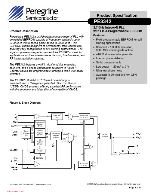
Document No. 70-0091-04 │ ©2005-8 Peregrine Semiconductor Corp. All rights reserved.(UTSi®) CMOS process, offering excellent RF performance with the economy and integration of conventional CMOS.Figure 1. Block DiagramPD_U PD_DLDCextPE3342 Product SpecificationProduct SpecificationPE3342Document No. 70-0091-04 │ ©2005-8 Peregrine Semiconductor Corp. All rights reserved.Table 4. Operating RangesTable 3. Absolute Maximum RatingsSymbol Parameter/Conditions Min Max UnitsV DD Supply voltage –0.3 +4.0 V V I Voltage on any digital input–0.3 V DD +0.3 V T StgStorage temperature range–65+85°CSymbol Parameter/Conditions MinMax UnitsV DD Supply voltage 2.85 3.15 V T A Operatingambient temperature range-40 85 °CSymbol Parameter/Conditions Min Max UnitsV ESD ESD voltage human body model (Note 1)1000 V V ESD(V PP )ESD voltage human body model (Note 1)200VNote 1: Periodically sampled, not 100% tested. Tested per MIL-STD-883, M3015 C2Table 5. ESD RatingsElectrostatic Discharge (ESD) Precautions When handling this UltraCMOS™ device, observe the same precautions that you would use with other ESD-sensitive devices. Although this device contains circuitry to protect it from damage due to ESD, precautions should be taken to avoid exceeding the specified rating in Table 4. Latch-Up AvoidanceUnlike conventional CMOS devices, UltraCMOS™ devices are immune to latch-up.Exceeding absolute maximum ratings may cause permanent damage. Operation should berestricted to the limits in the Operating Ranges table. Operation between operating rangemaximum and absolute maximum for extended periods may reduce reliability.PE3342 Product SpecificationProduct SpecificationPE3342Document No. 70-0091-04 │©2005-8 Peregrine Semiconductor Corp. All rights reserved.Table 7. AC CharacteristicsV DD = 3.0 V, -40° C < T A < 85° C, unless otherwise specifiedSymbol ParameterConditions Min Max UnitsControl Interface and Registers (see Figure 4)f Clk Serial data clock frequency (Note 1)10MHz t ClkH Serial clock HIGH time 30 ns t ClkL Serial clock LOW time30 ns t DSU Data set-up time to Clock rising edge 10 ns t DHLD Data hold time after Clock rising edge 10 ns t PW S_WR pulse width30 ns t CWR Clock rising edge to S_WR rising edge 30 ns t CE Clock falling edge to E_WR transition 30 ns t WRC S_WR falling edge to Clock rising edge 30 ns t EC E_WR transition to Clock rising edge30nsEEPROM Erase/Write Programming (see Figures 5 & 6)t EESU EELoad rising edge to V PP rising edge 500 ns t EEPW V PP pulse width25 30 ms t VPPV PP pulse rise and fall times(Note 2) 1 µsMain Divider (Including Prescaler)F In Operating frequency300 2700 MHz F In Operating frequency Speed-grade option (Note 3) 300 3000 MHz P FInInput level rangeExternal AC coupling-55dBmMain Divider (Prescaler Bypassed)F In Operating frequency (Note 4)50 270 MHz P FInInput level rangeExternal AC coupling (Note 4)-55dBmReference Dividerf r Operating frequency(Note 5)100MHz P fr Reference input power (Note 4)Single ended input-2dBmPhase Detectorf cComparison frequency(Note 6)20MHzSSB Phase Noise (F in = 1.3 GHz, f r = 10 MHz, f c = 1.25 MHz, LBW = 70 kHz, V DD = 3.0 V, Temp = -40° C )100 Hz Offset -75 dBc/Hz1 kHz Offset-85dBc/HzNote 1: f Clk is verified during the functional pattern test. Serial programming sections of the functional pattern are clocked at 10 MHz to verify f Clkspecification.Note 2: Rise and fall times of the V PP programming voltage pulse must be greater than 1 µs.Note 3: The maximum frequency of operation can be extended to 3.0 GHz by ordering a special speed-grade option. Please refer to Table 14,Ordering Information, for ordering details.Note 4: CMOS logic levels can be used to drive F In input if DC coupled and used in Prescaler Bypass mode. Voltage input needs to be a minimumof 0.5 Vp-p. For optimum phase noise performance, the reference input falling edge rate should be faster than 80 mV/ns. No minimum frequency limit exists when operated in this mode.Note 5: CMOS logic levels can be used to drive reference input if DC coupled. Voltage input needs to be a minimum of 0.5 Vp-p. For optimumphase noise performance, the reference input falling edge rate should be faster than 80 mV/ns.Note 6: Parameter is guaranteed through characterization only and is not tested.PE3342 Product SpecificationProduct SpecificationPE3342Document No. 70-0091-04 │ ©2005-8 Peregrine Semiconductor Corp. All rights reserved.Lock Detect OutputA lock detect signal is provided at pin LD, via the pin C EXT (see Figure 1). C EXT is the logical “NAND” of PD_U and PD_D waveforms, driven through a series 2k ohm resistor. When the loop is locked, this output will be HIGH with narrow pulses LOW. Connecting C EXT to an external shunt capacitor provides integration of this signal.The C EXT signal is sent to the LD pin through an internal inverting comparator with an open drain output. Thus LD is an “AND” function of PD_U and PD_D .Serial Data PortThe Serial Data Port allows control data to beentered into the device. This data can be directed into one of three registers: the Enhancementregister, the Primary register, and the EE register. Table 7 defines the control line settings required to select one of these destinations.Input data presented on pin 5 (Data) is clocked serially into the designated register on the rising edge of Clock. Data is always loaded LSB (B 0) first into the receiving register. Figure 4 defines the timing requirements for this process .Table 8. Serial InterfaceS_WR E_WR EELoadRegister Loaded0 0 0 Primary Register 0 1 0 Enhancement Register 0X1EE RegisterFigure 4. Serial Interface Timing DiagramE_WREELoadDataClockS_WRPE3342 Product SpecificationProduct SpecificationPE3342Document No. 70-0091-04 │ ©2005-8 Peregrine Semiconductor Corp. All rights reserved.Enhancement RegisterThe Enhancement Register is a buffered serial shift register, loaded from the Serial Data Port. It activates special test and operating modes in the PLL. The bit assignments for these modes are shown in Table 11.The functions of these Enhancement Register bits are shown in Table 12. A function becomes active when its corresponding bit is set HIGH. Note that bits 1, 2, 5, and 6 direct various data to the Dout pin, and for valid operation no more than one should be set HIGH simultaneously .The Enhancement Register is buffered to prevent inadvertent control changes during serial loading. Data that has been loaded into the register is cap-tured in the buffer and made available to the PLL on the falling edge of E_WR.A separate control line is provided to enable and disable the Enhancement mode. Functions are enabled by taking the ENH control line LOW. Note: The enhancement register bit values are unknown during power up. To avoid enabling the enhancement mode during power up, set the Enh pin high (“1”) until the enhancement register bit values are programmed to a known state.Table 12. Enhancement Register Bit AssignmentsReservedEE Register Outputf p outputPower downCounter loadMSEL outputf c outputReservedB 0B 1B 2B 3B 4B 5B 6B 7Table 13. Enhancement Register FunctionsBit FunctionDescriptionBit 0 Reserved Program to 0Bit 1 EE Register OutputAllows the contents of the EE Register to be serially shifted out Dout, LSB (B 0) first. Data is shifted on rising edge of Clock. Bit 2 f p output Provides the M counter output at Dout.Bit 3 Power down Powers down all functions except programming interface. Bit 4 Counter load Immediate and continuous load of counter programming.Bit 5 MSEL output Provides the internal dual modulus prescaler modulus select (MSEL) at Dout. Bit 6 f c output Provides the R counter output at Dout. Bit 7ReservedProgram to 0PE3342 Product Specification分销商库存信息:PSC3342-543342-563342-07。
ADE7878ACPZ;ADE7854ACPZ;ADE7854ACPZ-RL;ADE7858ACPZ-RL;ADE7868ACPZ-RL;中文规格书,Datasheet资料

Polyphase Multifunction Energy Metering ICADE7854/ADE7858/ADE7868/ADE7878 Rev. EInformation furnished by Analog Devices is believed to be accurate and reliable. However, noresponsibility is assumed by Analog Devices for its use, nor for any infringements of patents or other rights of third parties that may result from its use. Specifications subject to change without notice. No license is granted by implication or otherwise under any patent or patent rights of Analog Devices. T rademarks and registered trademarks are the property of their respective owners. One Technology Way, P.O. Box 9106, Norwood, MA 02062-9106, U.S.A. Tel: 781.329.4700 Fax: 781.461.3113 ©2010–2011 Analog Devices, Inc. All rights reserved.FEATURESHighly accurate; supports EN 50470-1, EN 50470-3,IEC 62053-21, IEC 62053-22, and IEC 62053-23 standards Compatible with 3-phase, 3- or 4-wire (delta or wye), and other 3-phase servicesSupplies total (fundamental and harmonic) active, reactive (ADE7878, ADE7868, and ADE7858 only), and apparent energy, and fundamental active/reactive energy (ADE7878 only) on each phase and on the overall systemLess than 0.1% error in active and reactive energy over a dynamic range of 1000 to 1 at T A = 25°CLess than 0.2% error in active and reactive energy over a dynamic range of 3000 to 1 at T A = 25°CSupports current transformer and di/dt current sensors Dedicated ADC channel for neutral current input (ADE7868 and ADE7878 only)Less than 0.1% error in voltage and current rms over a dynamic range of 1000 to 1 at T A = 25°CSupplies sampled waveform data on all three phases and on neutral currentSelectable no load threshold levels for total and fundamental active and reactive powers, as well as for apparent powersLow power battery mode monitors phase currents for antitampering detection (ADE7868 and ADE7878 only) Battery supply input for missing neutral operationPhase angle measurements in both current and voltage channels with a typical 0.3° errorWide-supply voltage operation: 2.4 V to 3.7 VReference: 1.2 V (drift 10 ppm/°C typical) with external overdrive capabilitySingle 3.3 V supply40-lead lead frame chip scale package (LFCSP), Pb-free Operating temperature: −40°C to +85°CFlexible I2C, SPI, and HSDC serial interfaces APPLICATIONSEnergy metering systemsGENERAL DESCRIPTIONThe ADE7854/ADE7858/ADE7868/ADE7878 are high accuracy, 3-phase electrical energy measurement ICs with serial interfaces and three flexible pulse outputs. The ADE78xx devices incorporate second-order sigma-delta (Σ-Δ) analog-to-digital converters (ADCs), a digital integrator, reference circuitry, and all of the signal processing required to perform total (fundamental and harmonic) active, reactive (ADE7878, ADE7868, and ADE7858), and apparent energy measurement and rms calcu-lations, as well as fundamental-only active and reactive energy measurement (ADE7878) and rms calculations. A fixed function digital signal processor (DSP) executes this signal processing. The DSP program is stored in the internal ROM memory. The ADE7854/ADE7858/ADE7868/ADE7878 are suitable for measuring active, reactive, and apparent energy in various 3-phase configurations, such as wye or delta services, with both three and four wires. The ADE78xx devices provide system calibration features for each phase, that is, rms offset correction, phase calibration, and gain calibration. The CF1, CF2, and CF3 logic outputs provide a wide choice of power information: total active, reactive, and apparent powers, or the sum of the current rms values, and fundamental active and reactive powers.The ADE7854/ADE7858/ADE7868/ADE7878 contain wave-form sample registers that allow access to all ADC outputs. The devices also incorporate power quality measurements, such as short duration low or high voltage detections, short duration high current variations, line voltage period measurement, and angles between phase voltages and currents. Two serial interfaces, SPI and I2C, can be used to communicate with the ADE78xx. A dedicated high speed interface, the high speed data capture (HSDC) port, can be used in conjunction with I2C to provide access to the ADC outputs and real-time power information. The ADE7854/ADE7858/ADE7868/ADE7878 also have two interrupt request pins, IRQ0 and IRQ1, to indicate that an enabled interrupt event has occurred. For the ADE7868/ADE7878, three specially designed low power modes ensure the continuity of energy accumulation when the ADE7868/ADE7878 is in a tam-pering situation. See for a quick reference chart listing each part and its functions. The ADE78xx are available in the 40-lead LFCSP, Pb-free package.Table 1Table 1. Part ComparisonPart No. WATT VARIRMS,VRMS,andVA di/dtFundamentalWATT andVARTamperDetectand LowPowerModes ADE7878 Yes Yes Yes Yes Yes Yes ADE7868 Yes Yes Yes Yes No Yes ADE7858 Yes Yes Yes Yes No No ADE7854 Yes No Yes Yes No NoADE7854/ADE7858/ADE7868/ADE7878Rev. E | Page 2 of 96TABLE OF CONTENTSFeatures..............................................................................................1 Applications.......................................................................................1 General Description.........................................................................1 Revision History...............................................................................3 Functional Block Diagrams.............................................................4 Specifications.....................................................................................8 Timing Characteristics..............................................................11 Absolute Maximum Ratings..........................................................14 Thermal Resistance....................................................................14 ESD Caution................................................................................14 Pin Configuration and Function Descriptions...........................15 Typical Performance Characteristics...........................................17 Test Circuit......................................................................................19 Terminology....................................................................................20 Power Management........................................................................21 PSM0—Normal Power Mode (All Parts)................................21 PSM1—Reduced Power Mode (ADE7868, ADE7878 Only)21 PSM2—Low Power Mode (ADE7868, ADE7878 Only).......21 PSM3—Sleep Mode (All Parts)................................................22 Power-Up Procedure..................................................................24 Hardware Reset...........................................................................25 Software Reset Functionality....................................................25 Theory of Operation......................................................................26 Analog Inputs..............................................................................26 Analog-to-Digital Conversion..................................................26 Current Channel ADC...............................................................27 di/dt Current Sensor and Digital Integrator..............................29 Voltage Channel ADC...............................................................30 Changing Phase Voltage Datapath...........................................31 Power Quality Measurements...................................................32 Phase Compensation.................................................................37 Reference Circuit........................................................................39 Digital Signal Processor.............................................................39 Root Mean Square Measurement.............................................40 Active Power Calculation..........................................................44 Reactive Power Calculation—ADE7858, ADE7868, ADE7878 Only..............................................................................................49 Apparent Power Calculation.....................................................54 Waveform Sampling Mode.......................................................57 Energy-to-Frequency Conversion............................................57 No Load Condition....................................................................61 Checksum Register.....................................................................63 Interrupts.....................................................................................64 Serial Interfaces..........................................................................65 ADE7878 Evaluation Board......................................................72 Die Version..................................................................................72 Silicon Anomaly.............................................................................73 ADE7854/ADE7858/ADE7868/ADE7878 FunctionalityIssues............................................................................................73 Functionality Issues....................................................................73 Section 1. ADE7854/ADE7858/ADE7868/ADE7878Functionality Issues....................................................................74 Registers List...................................................................................75 Outline Dimensions.......................................................................93 Ordering Guide.. (93)ADE7854/ADE7858/ADE7868/ADE7878Rev. E | Page 3 of 96REVISION HISTORY4/11—Rev. D to Rev. EChanges to Input Clock FrequencyParameter, Table 2..............10 Changes to Current RMS Offset Compensation Section..........42 Changes to Voltage RMS Offset Compensation Section...........44 Changes to Note 2, Table 30...........................................................77 Changes to Address 0xE707, Table 33..........................................80 Changes to Table 45........................................................................87 Changes to Table 46........................................................................88 Changes to Bit Location 7:3, Default Value, Table 54.. (92)2/11—Rev. C to Rev. DChanges to Figure 1...........................................................................4 Changes to Figure 2...........................................................................5 Changes to Figure 3...........................................................................6 Changes to Figure 4...........................................................................7 Changes to Table 2............................................................................8 Changed SCLK Edge to HSCLK Edge, Table 5...........................13 Change to Current Channel HPF Section...................................28 Change to di/dt Current Sensor and Digital IntegratorSection..............................................................................................30 Changes to Digital Signal Processor Section...............................39 Changes to Figure 59......................................................................44 Changes to Figure 62......................................................................47 Changes to Figure 65......................................................................49 Changes to Figure 66......................................................................52 Changes to Line Cycle Reactive Energy Accumulation Mode Section and to Figure 67.................................................................53 No Load Detection Based On Total Active, Reactive Powers Section..............................................................................................61 Change to Equation 50...................................................................63 Changes to the HSDC Interface Section......................................70 Changes to Figure 87 and Figure 88.............................................71 Changes to Figure 89......................................................................72 Changes to Table 30 (77)11/10—Rev. B to Rev. CChange to Signal-to-Noise-and-Distortion Ratio, SINADParameter, Table 1.............................................................................9 Changes to Figure 18......................................................................18 Changes to Figure 22......................................................................19 Changes to Silicon Anomaly Section............................................72 Added Table 28 to Silicon Anomaly Section, RenumberedTables Sequentially..........................................................................73 8/10—Rev. A to Rev. BChanges to Figure 1..........................................................................4 Changes to Figure 2..........................................................................5 Changes to Figure 3..........................................................................6 Changes to Figure 4..........................................................................7 Change to Table 8............................................................................16 Changes to Power-Up Procedure Section....................................23 Changes to Equation 6 and Equation 7........................................33 Changes to Equation 17.................................................................43 Changes to Active Power Offset Calibration Section.................45 Changes to Figure 63......................................................................46 Changes to Reactive Power Offset Calibration Section.............49 Changes to Figure 82......................................................................65 Added Silicon Anomaly Section, Renumbered TablesSequentially (71)3/10—Rev. 0 to Rev. AAdded ADE7854, ADE7858, and ADE7878..................Universal Reorganized Layout...........................................................Universal Added Table 1, Renumbered Sequentially.....................................1 Added Figure 1, Renumbered Sequentially...................................3 Added Figure 2..................................................................................4 Added Figure 3..................................................................................5 Changes to Specifications Section..................................................7 Changes to Figure 9........................................................................14 Changes to Table 8..........................................................................14 Changes to Typical Performance Characteristics Section.........16 Changes to Figure 22......................................................................18 Changes to the Power Management Section...............................20 Changes to the Theory of Operation Section..............................25 Changes to Figure 31 and Figure 32.............................................27 Change to Equation 28...................................................................47 Changes to Figure 83......................................................................66 Changes to Figure 86......................................................................68 Changes to the Registers List Section...........................................72 Changes to Ordering Guide.. (91)2/10—Revision 0: Initial VersionADE7854/ADE7858/ADE7868/ADE7878Rev. E | Page 4 of 96FUNCTIONAL BLOCK DIAGRAMSR E S E TR E F C L K I C L K O U I A I A V A I B I B V B I C I C V C V S C L K/S C LS D AH S DA08510-204Figure 1. ADE7854 Functional Block DiagramADE7854/ADE7858/ADE7868/ADE7878Rev. E | Page 5 of 96R E S E TR E F C L K I C L K O U I A I A V A I B I B V B I C I C V C V S C L K/S C LS D AH S DA08510-203Figure 2. ADE7858 Functional Block DiagramADE7854/ADE7858/ADE7868/ADE7878Rev. E | Page 6 of 96R E S E TR E F C L K I C L K O U I A I A V A I B I B V B I C I C V C V S C L K/S C LS D AH S DAI N I N 08510-202Figure 3. ADE7868 Functional Block DiagramADE7854/ADE7858/ADE7868/ADE7878Rev. E | Page 7 of 96R E S E TR E F C L K I C L K O U I A I A V A I B I B V B I C I C V C V S C L K/S C LS D AH S DAI N I N 08510-201Figure 4. ADE7878 Functional Block DiagramADE7854/ADE7858/ADE7868/ADE7878Rev. E | Page 8 of 96SPECIFICATIONSVDD = 3.3 V ± 10%, AGND = DGND = 0 V , on-chip reference, CLKIN = 16.384 MHz, T MIN to T MAX = −40°C to +85°C. Table 2.Parameter 1, 2 Min Typ Max Unit Test Conditions/Comments ACCURACYActive Energy MeasurementActive Energy Measurement Error (per Phase)Total Active Power0.1%Over a dynamic range of 1000 to 1, PGA = 1, 2, 4; integrator off0.2 % Over a dynamic range of 3000 to 1, PGA = 1, 2, 4;integrator off0.1 % Over a dynamic range of 500 to 1, PGA = 8, 16;integrator onFundamental Active Power (ADE7878 Only) 0.1% Over a dynamic range of 1000 to 1, PGA = 1, 2, 4; integrator off 0.2 % Over a dynamic range of 3000 to 1, PGA = 1, 2, 4;integrator off0.1 % Over a dynamic range of 500 to 1, PGA = 8, 16;integrator onPhase Error Between Channels Line frequency = 45 Hz to 65 Hz, HPF on Power Factor (PF) = 0.8 Capacitive ±0.05 Degrees Phase lead 37° PF = 0.5 Inductive ±0.05 Degrees Phase lag 60° AC Power Supply Rejection VDD = 3.3 V + 120 mV rms/120 Hz, IPx = VPx =±100 mV rmsOutput Frequency Variation 0.01 % DC Power Supply Rejection VDD = 3.3 V ± 330 mV dc Output Frequency Variation 0.01 %Total Active Energy MeasurementBandwidth2 kHz REACTIVE ENERGY MEASUREMENT(ADE7858, ADE7868, AND ADE7878)Reactive Energy Measurement Error(per Phase)Total Active Power 0.1 % Over a dynamic range of 1000 to 1, PGA = 1, 2, 4;integrator off0.2 % Over a dynamic range of 3000 to 1, PGA = 1, 2, 4;integrator off0.1 % Over a dynamic range of 500 to 1, PGA = 8, 16;integrator onFundamental Active Power (ADE7878 Only) 0.1% Over a dynamic range of 1000 to 1, PGA = 1, 2, 4; integrator off 0.2 % Over a dynamic range of 3000 to 1, PGA = 1, 2, 4;integrator off0.1 % Over a dynamic range of 500 to 1, PGA = 8, 16;integrator onPhase Error Between Channels Line frequency = 45 Hz to 65 Hz, HPF on PF = 0.8 Capacitive ±0.05 Degrees Phase lead 37° PF = 0.5 Inductive ±0.05 Degrees Phase lag 60° AC Power Supply Rejection VDD = 3.3 V + 120 mV rms/120 Hz, IPx = VPx =±100 mV rmsOutput Frequency Variation 0.01 %ADE7854/ADE7858/ADE7868/ADE7878Rev. E | Page 9 of 96Parameter 1, 2Min Typ Max Unit Test Conditions/Comments DC Power Supply Rejection VDD = 3.3 V ± 330 mV dc Output Frequency Variation0.01% Total Reactive Energy Measurement Bandwidth2kHzRMS MEASUREMENTSI rms and V rms Measurement Bandwidth2 kHz I rms and V rms Measurement Error (PSM0 Mode)0.1 % Over a dynamic range of 1000 to 1, PGA = 1 MEAN ABSOLUTE VALUE (MAV)MEASUREMENT (ADE7868 AND ADE7878)I mav Measurement Bandwidth (PSM1 Mode)260 Hz I mav Measurement Error (PSM1 Mode) 0.5 % Over a dynamic range of 100 to 1, PGA = 1, 2, 4, 8 ANALOG INPUTSMaximum Signal Levels±500mV peakDifferential inputs between the following pins: IAP and IAN, IBP and IBN, ICP and ICN; single-ended inputs between the following pins: VAP and VN, VBP and VN, VCP and VN Input Impedance (DC)IAP , IAN, IBP , IBN, ICP , ICN, VAP , VBP , and VCP Pins 400 kΩVN Pin130 kΩADC Offset Error±2 mV PGA = 1, uncalibrated error, see the Terminology sectionGain Error±4 % External 1.2 V referenceWAVEFORM SAMPLINGSampling CLKIN/2048, 16.384 MHz/2048 = 8 kSPS Current and Voltage Channels See the Waveform Sampling Mode section Signal-to-Noise Ratio, SNR70 dB PGA = 1 Signal-to-Noise-and-Distortion Ratio, SINAD60 dB PGA = 1Bandwidth (−3 dB)2 kHz TIME INTERVAL BETWEEN PHASESMeasurement Error0.3 Degrees Line frequency = 45 Hz to 65 Hz, HPF on CF1, CF2, CF3 PULSE OUTPUTSMaximum Output Frequency 8 kHz WTHR = VARTHR = VATHR = PMAX = 33,516,139 Duty Cycle50%If CF1, CF2, or CF3 frequency > 6.25 Hz and CFDEN is even and > 1(1 + 1/CFDEN) × 50% If CF1, CF2, or CF3 frequency > 6.25 Hz andCFDEN is odd and > 1Active Low Pulse Width 80 ms If CF1, CF2, or CF3 frequency < 6.25 Hz Jitter 0.04 % For CF1, CF2, or CF3 frequency = 1 Hz andnominal phase currents are larger than 10% of full scaleREFERENCE INPUT REF IN/OUT Input Voltage Range 1.1 1.3 V Minimum = 1.2 V − 8%; maximum = 1.2 V + 8% Input Capacitance 10 pF ON-CHIP REFERENCE Nominal 1.207 V at the REF IN/OUT pin at T A = 25°C PSM0 and PSM1 Modes Reference Error ±2 mV Output Impedance 1.2 kΩ Temperature Coefficient 10 50 ppm/°C Maximum value across full temperature rangeof −40°C to +85°CADE7854/ADE7858/ADE7868/ADE78781 See the Typical Performance Characteristics section.2 See the Terminology section for a definition of the parameters.Rev. E | Page 10 of 96分销商库存信息:ANALOG-DEVICESADE7878ACPZ ADE7854ACPZ ADE7854ACPZ-RL ADE7858ACPZ-RL ADE7868ACPZ-RL ADE7878ACPZ-RL ADE7858ACPZ ADE7868ACPZ EVAL-ADE7878EBZ。
- 1、下载文档前请自行甄别文档内容的完整性,平台不提供额外的编辑、内容补充、找答案等附加服务。
- 2、"仅部分预览"的文档,不可在线预览部分如存在完整性等问题,可反馈申请退款(可完整预览的文档不适用该条件!)。
- 3、如文档侵犯您的权益,请联系客服反馈,我们会尽快为您处理(人工客服工作时间:9:00-18:30)。
SYMBOL
(mm) (inch)
A
B
C
d
D
0.75 ± 0.10 1.15 ± 0.10 0.60 ± 0.10 1.55 + 0.10 178 ± 1
0.026 ± 0.004 0.045 ± 0.004 0.024 ± 0.004 0.061 + 0.004 7.008 ± 0.04
D1
D2
60.0 MIN. 13.0 ± 0.20
0.069 ± 0.004 0.138 ± 0.002 0.157 ± 0.004 0.157 ± 0.004 0.079 ± 0.004 0.009 ± 0.002 0.315 ± 0.008 0.531 MAX.
QW-A1122
/
Comchip Technology CO., LTD.
0.500
0.020
0.700
0.028
1.250
0.049
0.250
0.010
Standard Package
Case Type
Qty per Reel Reel Size
(Pcs)
(inch)
0402/SOD-923F
5000
7
BF
D A E
C B
QW-A1122
/
2.362 MIN. 0.512 ± 0.008
0402 (SOD-923F)
SYMBOL
(mm) (inch)
E
F
P
P0
P1
T
W
W1
1.75 ± 0.10 3.50 ± 0.05 4.00 ± 0.10 4.00 ± 0.10 2.00 ± 0.10 0.22 ± 0.05 8.00 ± 0.20 13.5 MAX.
VR(RMS)
21
V
Average forward rectified current
IO
200 mA
Repetitive peak forward current
IFRM
0.3 A
Forward current,surge peak
8.3 ms single half sine-wave superimposed on rate load(JEDEC method)
Parameter
Conditions
Symbol Min Typ Max Unit
Forward voltage Reverse current
IF = 0.1mA IF = 1mA IF = 10mA IF = 30mA IF = 100mA
VR = 25V
0.24
0.32
VF
0.4 V
0.5
1
Mechanical data
-Case: 0402/SOD-923F standard package, molded plastic.
-Terminals: Gold plated, solderable per MIL-STD-750,method 2026.
-Marking Code: Cathode band & BF -Mounting position: Any. -Weight: 0.001 gram(approx.).
Maximum
Rating
(at
O
TA=25 C
unless
otherwise
noted)
Parameter
Peak reverse voltage Reverse voltage
Conditions
Symbol Min Typ Max Unit
VRM
30
V
VR
30
V
RMS reverse voltage
Average forward current(%)
Fig.4 - Current derating curve
120 Mounting on glass epoxy PCBs
100
80
60
40
20
0
0
25
50
75 100 125 150
O
Ambient temperature ( C)
Capacitance between terminals (PF)
IFSM
0.6 A
Power dissipation
PD
125 mW
Storage temperature
TSTG
-65
+125
O
C
Junction temperature
Tj
+125
O
C
Electrical
Characteristics
(at
O
TA=25 C
unless
otherwise
noted)
Comchip Technology CO., LTD.
REV:B Page 4
分销商库存信息:
COMCHIP CDBQR54
O
25 C
O
-25 C
5
10
15
20
25 30
Reverse voltage (V)
Fig.3 - Capacitance between terminals characteristics
14
f=1MHz
12
O
TA=25 C
10
8
6
4
2
0
0
5
10 15 20 25 30
Reverse voltage (V)
D2
D1 D
W1
Trailer
Device
Leader
.......
.......
.......
.......
End
.......
.......
.......
.......
10 pitches (min)
10 pitches (min)
Start
Direction of Feed
0402 (SOD-923F)
0402/SOD-923F
0.041(1.05) 0.037(0.95)
0.026(0.65) 0.022(0.55)
0.012(0.30) Typ.
0.022(0.55) 0.018(0.45)
0.020(0.50) Typ.
Dimensions in inches and (millimeter)
QW-A1122
/
Comchip Technology CO., LTD.
REV:B Page 2
SMD Schottky Barrier Diode
Reel Taping Specification
P0
d
T
P1
E
Index hole
F
B
W
Polarity
C
P
A
o
12 0
1000
100
10
1
O
C
O
C
O
C
O
C
-25
25
75
125
0.1 0
0.2
0ward voltage (V)
Reverse current ( A )
Fig. 2 - Reverse characteristics
1m
100u
O
125 C
10u O 75 C
1u
100n
10n 0
Comchip Technology CO., LTD.
REV:B Page 1
Forward current (mA )
SMD Schottky Barrier Diode
RATING AND CHARACTERISTIC CURVES (CDBQR54)
Fig. 1 - Forward characteristics
IR
2
uA
Capacitance between terminals f = 1 MHz, and 1 VDC reverse voltage
CT
10 pF
Reverse recovery time
IF=IR=10mA,Irr=0.1xIR,RL=100 Ohm
Trr
5
nS
QW-A1122
/
REV:B Page 3
SMD Schottky Barrier Diode
Marking Code
Part Number Marking Code
CDBQR54
BF
Suggested PAD Layout
SIZE
A B C D E
0402/SOD-923F
(mm) 0.750
(inch) 0.030
SMD Schottky Barrier Diode
CDBQR54
Io = 200 mA VR = 30 Volts RoHS Device
Features
-Low forward voltage. -Designed for mounting on small surface. -Extremely thin / leadless package. -Majority carrier conduction.