升压XC9110_11_V1
XC9119 DCDC升压芯片

XC9119D10A Series1MHz, PWM Controlled,Step-Up DC/DC Converter, Ceramic Capacitor CompatibleETR0408_008■GENERAL DESCRIPTIONThe XC9119D10A series is 1MHz, PWM controlled step-up DC/DC converter, designed to allow the use of ceramic capacitors. With a built-in 2.0Ω switching transistor, the XC9119D10A series can easily provide a step-up operation by using only a coil, a diode, a capacitor, and a resistor, connected externally.Since output voltage up to 19.5V (Maximum Lx operating voltage: 20V) can be derived with reference voltage supply of 1.0V (±2.0%) and external components, the series can easily supply high voltage for various general-purpose power supplies, LCD panels and organic EL displays. With a high switching frequency of 1.0MHz, a low profile and small board area solution can be achieved using a chip coil andan ultra small ceramic output capacitor.With the current limit function (400mA (TYP .): V DD =3.6V), a peak current, which flows through built-in driver transistors can be limited. Soft-start time can be adjusted by external resistors and capacitors. The stand-by function enables the output to be turned off (CE ’L’), that is, the supply current will be less than 1.0⎧A.■TYPICAL APPLICATION CIRCUIT■APPLICATIONS●Organic electroluminescence display (OELD)●Power supplies for LCDs ●Multi-function power supplies■FEATURESOperating Voltage Range : 2.5V ~ 6.0V Output Voltage Range : Up to 19.5V externally set-up: Reference voltage 1.0V +2.0%Oscillation Freq uency : 1.0MHz ±20%ON Resistance : 2.0Ω (V DD =3.6V, V DS=0.4V) Efficiency : 86%(V OUT =15V, V DD =3.6V, I OUT =10mA)Control : PWM control Stand-by function : I STB =1.0⎧A (MAX.)Load Capacitor : Low ESR ceramic capacitorUltra Small Packages : SOT-25, USP-6C Lx Limit Current : 400mA (V DD =3.6V)■TYPICAL PERFORMANCE CHARACTERISTICS○Efficiency vs. Output Current1020304050607080901000.11101001000Output Current: I OUT (mA)E f f i c i e n c y : EF F I (%)XC9119D10A1/182/18■PIN CONFIGURATIONSOT-25*The dissipation pad for the USP-6C package should be solder-plated in recommended mount pattern and metal masking so as to enhance mounting strength and heat resistance. If the pad needs to be connected to other pins, itshould be connected to the V SSpin. USP-6C(BOTTOM VIEW)(TOP VIEW)PIN NUMBER SOT-25 USP-6CPIN NAMEFUNCTION1 2 Lx Switch2 3 V SS Ground 3 1 FB Voltage Feedback 4 6CE/SS Chip Enable/ Soft Start5 4 V DD Power Input - 5NC No Connection■PIN ASSIGNMENT■CE PIN FUNCTIONCE/SS PINOPERATIONAL STATEH OperationL Shut-down ■PRODUCT CLASSIFICATION●Ordering InformationXC9119D ①②③④⑤-⑥(*1)DESIGNATOR DESCRIPTION SYMBOLDESCRIPTION①② Reference Voltage 10 FB voltage ③Oscillation FrequencyA1MHzMR SOT-25MR-G SOT-25 (Halogen & Antimony free)ER USP-6C ④⑤-⑥Packages Taping Type(*2)ER-GUSP-6C (Halogen & Antimony free)(*1)The “-G” suffix indicates that the products are Halogen and Antimony free as well as being fully EU RoHS compliant. (*2)The device orientation is fixed in its embossed tape pocket. For reverse orientation, please contact your local Torex sales office or representative. (Standard orientation: ④R-⑥, Reverse orientation: ④L-⑥)XC9119D10ASeries ■BLOCK DIAGRAMVDDL X FBVSS■ABSOLUTE MAXIMUM RATINGSTa = 25O CPARAMETER SYMBOL RATINGS UNITSV DD Pin Voltage V DD V SS – 0.3 ~ 7.0 VLx Pin Voltage V Lx V SS – 0.3 ~ 22.0 VFB Pin Voltage V FB V SS – 0.3 ~ 7.0 VCE Pin Voltage V CE V SS – 0.3 ~ 7.0 VLx Pin Current I Lx 1000 mASOT-25 250 Power Dissipation Pd mWUSP-6C 120Operating Temperature Range Topr - 40 ~ + 85 O CStorage Temperature Range Tstg - 55 ~ +125 O C3/18■ELECTRICAL CHARACTERISTICSXC9119D10AMR4/18PARAMETER SYMBOLCONDITIONSMIN.TYP .MAX.UNITCIRCUITTa = 25O CFB Voltage V FB - 0.980 1.000 1.020 V ① △V FB/Line Regulation 2.5<△V IN ・V FBV DD <6.0V - 0.05 0.20 %/V ①Supply Voltage V DD - 2.5 - 6.0 V ① Operation Start-upVoltageV ST1 I OUT =0mA - - 2.5 V ② Supply Current 1 I DD1 - 450 700 μA ② FB=2.0VSupply Current 2 I DD2 - 55 110 μA ②Stand-by Current I STB V CE =0V - - 1.0 μA ③ Oscillation Frequency f Same as I DD1 0.8 1.0 1.2 MHz ② OSCMaximum Duty RatioMAXDTYSame as I DD1 86 92 98 % ② Efficiency (*1) EFFIV IN =V DD =3.6V, V OUT =15V,I OUT =10mA- 86 - % ① Current Limit I LIM V DD =3.6V 310 400 750 mA ④ Lx Operating VoltageRangeV Lx V OUT =18V - - 20.0 V ①Lx Switch On Resistance R SWON V DD =3.6V, V Lx =0.4V, Rpull=10Ω- 2.0 4.0 Ω ②Lx Leak Current I LxL Same as I STB - - 1 μA ③Applied voltage to CE when Lx pinvoltage holding “H””L” level CE “High” Voltage V CEH 0.65 - - V ②Applied voltage to CE when Lx pinvoltage holding “H” levelCE “Low” Voltage V CEL - - 0.20 V ②Soft-Start FB=0.95V , Applied voltage to CEV SST 1.3 1.6 1.9 V ②when Lx voltage holding “H””L” level Threshold VoltageCE “High” Current I CEH Same as I DD2 -0.1 - 0.1 μA ③ CE “Low” Current I CEL Same as I STB -0.1 - 0.1 μA ③ FB “High” Current I FBH Same as I DD2 -0.1 - 0.1 μA ③ FB “Low” Current I FBL Same as I STB -0.1 - 0.1 μA ③Test Condition: Unless otherwise stated, V IN =3.0V, V CE =3.0V, Vpull=5.0V, Rpull=100Ω.NOTE:*1: EFFI={(output voltage x output current) / (input voltage) x (input current)} x 100 ■TYPICAL APPLICATION CIRCUITV IN VOUT5/18XC9119D10ASeries■OPERATIONAL EXPLANATIONThe XC9119D10A series consists of a reference voltage source, ramp wave circuit, error amplifier, PWM comparator, phasecompensation circuit, driver transistor, current limiter circuit and others. The series ICs compare, using the error amplifier, the voltage of the internal reference voltage source with the feedback voltage from the FB pin. Phase compensation is performedon the resulting error amplifier output, to input a signal to the PWM comparator to determine the turn-on time during switching. The PWM comparator compares, in terms of voltage level, the signal from the error amplifier with the ramp wave from the ramp wave circuit, and delivers the resulting output to the buffer drive circuit to cause the Lx pin to output a switching duty cycle. This process is continuously performed to ensure stable output voltage. The current feedback circuit detects the N-channel MOS driver transistor's current for each switching operation, and modulates the error amplifier output signal to provide multiple feedback signals. This enables a stable feedback loop even when a low ESR capacitor, such as a ceramic capacitor, is used, ensuring stable output voltage.<Reference Voltage Source>The reference voltage source provides the reference voltage to ensure stable output voltage of the IC.<Ramp Wave Circuit>The ramp wave circuit determines switching frequency. The 1MHz (TYP .) of frequency is fixed internally. Clock pulses generated in this circuit are used to produce ramp waveforms needed for PWM operation.<Error Amplifier>The error amplifier is designed to monitor output voltage. The amplifier compares the reference voltage with the FB pin voltage. When a voltage lower than the reference voltage is fed back, the output voltage of the error amplifier increases. Gain and frequency characteristics of the error amplifier output are fixed internally as an optimize signal. <Current Limit >The current limit circuit of the XC9119D10A series monitors the current flowing through the N-channel MOS driver transistor connected to the Lx pin, and features a combination of the constant-current type current limit mode and the duty cycle limit of the next pulse.①When the driver current is greater than a specific level, the constant-current type current limit function operates to turn off the pulses from the Lx pin at any given timing.②The IC controls the next pulse to be smaller than the first pulse.Current Limit Current Limit21LxILThe current will be off when the coil current reaches the value of the constant current limit.Limit some duty pulses after the limit.<CE Pin Function>The operation of the XC9119D10A series will enter into the shut down mode when a low level signal is input to the CE pin. During the shut down mode, the supply current is 0μA (TYP .), with high impedance at the Lx pin. The IC starts its operation with a high level signal to the CE pin. The input to the CE pin is a CMOS input and the sink current is 0μA (TYP .). The hysteresis between the chip enable and the chip disable is 50mV (TYP .). <Soft-Start Time>Soft-start function operates when capacitors and resistors are connected to the CE/SS pin. With the Vref voltage limited by the CE/SS pin start-up voltage and applying the input to the error amps, the operation maintains a balance between the two inputs of the error amps. and controls the Lx pin’s ON time so that it doesn’t increase more than is necessary. Depending of current limit function, load current, step-up ratio, and external components, the IC takes about 500uS to 5mS to attain the setting voltage after applying the CE ‘H’ voltage even though the R SS is 0Ω and a soft start capacitor C SS is not connected. (For a numerical constant, please refer to Note on Use.) For longer soft-start time, please connect R SS and C SS . Soft-start function operates while the CE pin voltage is between 0V to around 1.9V . Please be noted that if the CE/SS pin voltage does not start from 0V but is in intermediate potential when the power is turned on etc., soft start function may lose an effect and that will cause a high inrush current and ripple voltage.■OPERATIONAL EXPLANATION (Continued)<CE/SS (Pin No. 4): Chip Enable / Soft-Start Pin>Pin No. 4 can be used as in either chip enable (CE) pin or soft-start (SS) pin. The IC takes about 5ms at most to attain the setting voltage after starting operation (CE ‘H’) even though the R SS is 0Ω and the C SS is not connected.Soft-start function is good for setting a longer time than the start-up time when the R SS is 0Ω and the C SS is not connected. Soft-start operates while the CE pin voltage increases from 0V to around 1.9V . The following equation is used with the values of Vcont voltage, the R SS and the C SS . T = - C SS x R SS x In {(Vcont – 1.6) / Vcont}R SS =0Ω, No C SS , V IN =3.6V, V OUT =15V, I OUT =3mA1ch: V OUT2ch: CE0V (1ch) ⇒0V (2ch) ⇒Time:500uS/div.1ch:5V/div., 2ch:2V/div.●Start-up waveformwhen the R SS is 0Ω and the C SS is not connectedEx.) When C SS =0.1uF, R SS =220k Ω, Vcont=5V,T= - 0.1e – 6 x 220e3 x In{(5-1.6)/5} = 8.48msEx.) Reference Circuit 1: N-ch Open DrainON/OFF SignalCE/SS PinEx.) Reference Circuit 2: CMOS Logic (Low Supply Current)ON/OFF SignalCE/SS PinEx.) Reference Circuit 3: CMOS Logic (Low Supply Current), Quick-OffON/OFF SignalCE/SS Pin6/187/18XC9119D10ASeries■OPERATIONAL EXPLANATION (Continued)<Lx (Pin No. 1): Switch Pin>Please connect the anode of an Schottky barrier diode and inductor to the Lx pin. <FB (Pin No. 3): Voltage Feedback Pin>The reference voltage is 1.0V (TYP .). Output voltage is approximated by the following equation according to the value for two resistors (R FB1 and R FB2). The sum of the two resistors should be 1M Ω or less. V OUT = R FB1 / R FB2 + 1Output voltage should be set as to fill V OUT <(Maximum value of V Lx ) – (V F of Schottky diode).Please adjust the C FB value of the speed–up capacitor for phase compensation so that fzfb=1/(2πx C FB x R FB1) will be about 500Hz. According to the usage, adjusting the inductance value, the load capacity value, and so on to the most suitable operation.Typical example:V OUT R FB1 R FB2 C FB (V)(k Ω)(k Ω)(pF)3.3 300 130 1000 5.0 300 75 1000 7.0 180 30 1800 10.0 270 30 1200 15.0 510 36 510 18.0 510 30510<V DD (Pin No. 5): Power Supply Pin>Please connect an input by-pass capacitor (C IN ).●Application Information<Obtaining V DD from other source than V IN >In case that the input voltage V IN and power source V DD in the step-up circuit are isolated, the circuit starts step-up operations with the input voltage less than 2.5V when voltage from 2.5V to 6.0V is applied to the power source. Please connect more than 1uF of C DD between the V DD pin and the V SS pin as close as possible.Ex.) When VDD =3.6V, V IN =1.8V, V OUT =5.0V (R FB1=300k Ω, R FB2=75k Ω, C FB =1000pF, C L =10μF), the IC can operate upto I OUT =40mA.■NOTES ON USE1. Please do not exceed the value of stated absolute maximum ratings.2. The DC/DC converter performance is greatly influenced by not only the ICs’ characteristics, but also by those of the external components. Care must be taken when selecting the external components.3. Make sure that the PCB GND traces are as thick as possible, as variations in ground potential caused by high ground currents at the time of switching may result in instability of the IC.4. Please mount each external component as close to the IC as possible and use thick, short connecting traces to reduce the circuit impedance.5. Please set up the output voltage value so that the Lx pin voltage does not exceed 20V.■TEST CIRCUITS Circuit ①Circuit ②Circuit③V IN LxCE FBV SSAV1uFV FB220uFRpullOSCVCircuit ④VV IN10300Ω1. The measurement method of Lx On resistance R SWONUsing the circuit ②, Lx On resistance can be measured by adjusting Vpull voltage to set Lx voltage V Lx x 0.4V when the driver transistor is ON. The oscilloscope is used for measuring the Lx voltage when the driver transistor is ON.R SWON = 0.4 / {(Vpull – 0.4) / 10}2. The measurement method of current limit I LIMUsing the circuit ④, current limit I LIM can be calculate by the equation including Vpull voltage when FB voltage is decreased while Vpull voltage is adjusted and Lx voltage V Lx when the driver transistor is ON. The oscilloscope is used for measuring the Lx voltage when the driver transistor is ON.I LIM=(Vpull – V Lx) / Rpull8/189/18XC9119D10ASeries■TYPICAL PERFORMANCE CHARACTERISTICS(1) Output Voltage vs. Output Current9.09.510.010.511.00.11101001000Load current: I OUT (mA)O u t p u t v o l t a g e : V O U T (V )VIN=VDD=VCE,L=22uH(CDRH4D18C)SD:XBS104S14R,CIN=CL=4.7uF(Ceramic)4.74.84.95.05.15.25.30.11101001000Load current: I OUT (mA)Ou t p u t v o l t a g e : V O U T (V )VIN=VDD=VCE,L=4.7uH(CDRH4D18C)SD:XBS104S14R,CIN=CL=4.7uF(Ceramic)17.017.518.018.519.00.11101001000Load current: I OUT (mA)O u t p u t v o l t a g e : VO U T (V )VIN=VDD=VCE,L=22uH(CDRH4D18C)SD:XBS104S14R,CIN=CL=4.7uF(Ceramic)14.014.515.015.516.00.11101001000Load current I OUT (mA)O u t p u t v o l t a g e : V OU T (V )VIN=VDD=VCE,L=22uH(CDRH4D18C)SD:XBS104S14R,CIN=CL=4.7uF(Ceramic)(2) Efficiency vs. Output CurrentVOUT=5VVOUT=10V1020304050607080901000.11101001000Load current: I OUT (mA)E f f i c i e n c y : EF F I (%)VIN=VDD=VCE,L=4.7uH(CDRH4D18C)SD:XBS104S14R,CIN=CL=4.7uF(Ceramic)0.11101001000Load current: I OUT (mA)E f f i c i e n c y : EF F I (%)VIN=VDD=VCE,L=22uH(CDRH4D18C)SD:XBS104S14R,CIN=CL=4.7uF(Ceramic)■TYPICAL PERFORMANCE CHARACTERISTICS (Continued)(2) Efficiency vs. Output Current (Continued)VOUT=18VVOUT=15V1020304050607080901000.11101001000Load current: I OUT (mA)E f f i c i e n c y : EF F I (%)VIN=VDD=VCE,L=22uH(CDRH4D18C)SD:XBS104S14R,CIN=CL=4.7uF(Ceramic)1020304050607080901000.11101001000Load current: I OUT (mA)E f f i c i e n c y : EF F I (%)VIN=VDD=VCE,L=22uH(CDRH4D18C)SD:XBS104S14R,CIN=CL=4.7uF(Ceramic)VOUT=15VVOUT=15V01020304050607080901000.11101001000Load current: I OUT (mA)E f f i c i e n c y :E F F I (%)VIN=VDD=VCE=3.6V,L :CDRH4D18C SD:XBS104S14R,CIN=CL=4.7uF(Ceramic)1020304050607080901000.1110100Load current: I OUT (mA)E f f i c i e n c y :E F F I (%)VIN=VDD=VCE=3.6V,L =22uHSD:XBS104S14R,CIN=CL=4.7uF(Ceramic)(3) Ripple Voltage vs. Output CurrentVOUT=5VVOUT=10V10/18204060801000.11101001000Load current: I OUT (mA)R i p p l e V o l t a g e : V r (m V )VIN=VDD=VCE,L=4.7uH(CDRH4D18C)SD:XBS104S14R,CIN=CL=4.7uF(Ceramic)0.11101001000Load current: I OUT (mA)R i p p l e V o l t a g e : V r (m V )VIN=VDD=VCE,L=22uH(CDRH4D18C)SD:XBS104S14R,CIN=CL=4.7uF(Ceramic)11/18Series■TYPICAL PERFORMANCE CHARACTERISTICS (Continued)(3) Ripple Voltage vs. Output Current (Continued)VOUT=18VVOUT=15V204060801000.11101001000Load current: I OUT (mA)R i p p l e V o l t a g e : V r (m V )VIN=VDD=VCE,L=22uH(CDRH4D18C)SD:XBS104S14R,CIN=CL=4.7uF(Ceramic)0204060801000.11101001000Load current: I OUT (mA)R i p p l e V o l t a g e : V r (m V )VIN=VDD=VCE,L=22uH(CDRH4D18C)SD:XBS104S14R,CIN=CL=4.7uF(Ceramic)(4) Maximum Output Current vs. Input Voltage (5) Feedback Voltage vs. Chip Enable Voltage050100150200250300350400450234567Input Voltage V IN (V)M a x i m u m l o a d c u r r e n t :I O U T _M A X (m A )VIN=VDD=VCE=3.6V,SD:XBS104S14R 0.00.20.40.60.81.01.200.51 1.52Chip E nable Voltage: V CE (V)F e e d b a c k V o l t a g e : V F B (V )(6) Supply Current 1 vs. Supply Voltage(7) Supply Current 2 vs. Supply Voltage02004006008001000120023456Supply Voltage: V DD (V)S u p p l y C u r r e n t 1: ID D 1(uA )02040608010012014023456Supply Voltage: V DD (V)S u p p l y C u r r e n t 2: ID D 2(uA )■TYPICAL PERFORMANCE CHARACTERISTICS (Continued)(9) Maximum Duty Cycle vs. Supply Voltage(8) Oscillation Frequency vs. Supply Voltage0.60.70.80.911.11.21.323456Supply Voltage: V DD (V)O s c i l l a t i o n F r e q u e n c y : F o s c (M H z )8688909294969823456Supply Voltage: V DD (V)M a x i m u m D u t y C y c l e : M A X D T Y (%)(10) Stan-by Current vs. Supply Voltage (11) Lx ON Resistance vs. Supply Voltage0.00.20.40.60.81.023456Supply Voltage: VDD (V)S t a n d b y C u r r e n t : IS T B (uA )0.01.02.03.04.05.06.023456Supply Voltage: V DD (V)L x O N R e s i s t a n c e : RS WO N(Ω)(12) Current Limit vs. Supply Voltage (13) Feedback Voltage vs. Supply Voltage12/18010020030040050060070080090023456Supply Voltage: V DD (V)C u r r e n t L i m i t : IL I M (m A )13/18Series■TYPICAL PERFORMANCE CHARACTERISTICS (Continued)(14) CE ‘H’ Voltage vs. Supply Voltage(15) CE ‘L’ Voltage vs. Supply Voltage0.200.250.300.350.400.450.500.550.600.6523456Supply Voltage: V DD (V)C E 'H ' V o l t a g e : VC E H (V )0.200.250.300.350.400.450.500.550.600.6523456Supply Voltage: VDD(V)C E 'L ' V o l t a g e : V C E L (V )VFB=0V,Vpull=5V,Rpull=100 (16) Load Transient Response4.804.854.904.955.005.055.10Time (0.2msec/div)O u t p u t V o l t a g e : V O U T (V )102030405060L o a d c u r r e n t :I O U T (m A )VIN=VDD=VCE=3.6V,L :CDRH4D18C SD:XBS104S14R,CIN=CL=4.7uF(Ceramic)CFB=620pF(Ceramic),RFB1=510k ohm,RFB2=36k ohm4.804.854.904.955.005.055.10Time (1.0msec/div)O u t p u t V o l t a g e : V O U T (V )102030405060L o a d c u r r e n t :I O U T (m A )VIN=VDD=VCE=3.6V,L :CDRH4D18C SD:XBS104S14R,CIN=CL=4.7uF(Ceramic)14.8014.8514.9014.9515.0015.0515.10Time (2.0msec/div)O u t p u t V o l t a g e : V O U T (V )102030405060L o a d c u r r e n t :I O U T (m A )VIN=VDD=VCE,L=4.7uH(CDRH4D18C)SD:XBS104S14R,CIN=CL=4.7uF(Ceramic)14.8014.8514.9014.9515.0015.0515.10Time (0.5msec/div)O u t p u t V o l t a g e : V O U T (V )102030405060L o a d c u r r e n t :I O U T (m A )VIN=VDD=VCE,L=4.7uH(CDRH4D18C)SD:XBS104S14R,CIN=CL=4.7uF(Ceramic)■TYPICAL PERFORMANCE CHARACTERISTICS (Continued)(17) Maximum Output Current vs. Input Voltage020*********120140160123456Input Voltage VIN(V)M a x i m u m O u t p u t C u r r e n t :IO U T _M A X (m A )SD:XB01B04ABR,L=22uH(CDRH4D18C)VCE=VDD,CIN=4.7uF(Ceramic)CL=10uF(Ceramic)CFB=620pF(Ceramic),RFB1=510k ,RFB2=36k 0100200300400500123456Input Voltage VIN(V)M a x i m u m O u t p u t C u r r e n t : I O U T _M A X (m A )SD:XB01B04ABR,L=4.7uH(CDRH4D18C)VCE=VDD,CIN=4.7uF(Ceramic)CL=10uF(Ceramic)VOUT=5VVOUT=15V14/1815/18Series■PACKAGING INFORMATION●SOT-25●USP-6C■PACKAGING INFORMATION (Continued)●USP-6C Reference Pattern Layout ●USP-6C Reference Metal Mask Design16/18Series■MARKING RULE●SOT-25 ①represents product seriesMARK PRODUCT SERIESXC9119xxxxMxL②represents Lx overvoltage limitMARK Lx OVERVOLTAGE LIMIT PRODUCT SERIESD NotAvailableXC9119DxxxMx SOT-25(TOP VIEW)③represents oscillation frequencyMARK OSCILLATION FREQUENCY PRODUCT SERIESA 1MHz XC9119xxxAMx④represents production lot number0 to 9 and A to Z, or inverted characters 0 to 9 and A to Z repeated.(G, I, J, O, Q, W excepted)●USP-6C①represents product seriesMARK PRODUCT SERIESV XC9119xxxxDx②represents Lx overvoltage limitMARK Lx OVERVOLTAGE LIMIT PRODUCT SERIESD NotAvailable XC9119DxxxDx USP-6C ③④represents FB voltage(TOP VIEW)MARK③FB VOLTAGE (V) PRODUCT SERIES④1 0 1.0 XC9119x10xDx⑤represents oscillation frequencyMARK OSCILLATION FREQUENCY PRODUCT SERIESA 1MHz XC9119xxxADx⑥represents production lot number0 to 9 and A to Z repeated (G, I, J, O, Q, W excepted)* No character inversion used.17/1818/18。
Multis表计

Technical Data
Operating Voltage (U Aux)
Operating Range (∆U)
: Please look at labels on the device.
LV or HV three phase - Multi-Meter 96 x 96
MULTIS I30: Ammeter with simultaneous display MULTIS V30: Voltmeter
MULTIS L20: Simultaneous display on the 3 phases + neutral the most frequent values for an electrical installation or for monitoring generator sets.
Measuring Range
: 0,05 -10.000 A (with X5 CT)
0,07-200 A (with TCA15 (for MULTIS I10))
Current Transformer Ratio (Ct) : 5...10000 / 5 A and drCt (for MULTIS I10)
MULTIS I10 / I11 / V10 / F10 Do not try to clean the device with solvent or the like. Only clean the device with a dried cloth.
Supertex生产的HV9912升压变换器控制器的集成电路是一个闭环与峰值电流控制
Supertex生产的HV9912升压变换器控制器的集成电路是一个闭环与峰值电流控制、开关模式变换器的LED驱动器。
HV9912的内置功能克服了变换器的缺点,特别地,它有一个“切断MOSFET”驱动的输出端。
当短路或输入过电压时,由这个输出驱动的外置MOSFET可以切断LED串。
这个“切断MOSFET”还可以极大地提高变换器的PWM调光响应速度。
可见HV9912升压变换器控制器的工作原理可以如下文所示:HV9912内部的高电压调节器可将9~9OV的输入电压调节到7.75V的VDD电压,作为芯片的供电电源。
这个电压范围适于大多数的升压应用。
当降压电路和SEPIC电路需要精准的电流控制时也可以使用此芯片。
在高压降压变换应用中,输入端可串联一个稳压二极管,以便承受更高的操作电压或减小芯片的功率损耗。
当外部电压源通过一个低压(>IOV)低电流二极管馈通时,芯片的VDD端可以过驱动。
当外部电压小于内部电压时,二极管可以防止HV9912损坏。
能加在HV9912的VDD引脚的最高稳态电压是l2V(瞬时额定电压为13.5V)。
考虑到二极管的正向压降,理想的电源电压应为l2V正负5%。
HV9912升压变换器控制器包含一个1.25V、精度为2%的带缓冲的参考电压。
通过REF、IREF和CLIM引脚间连接的分压器网络,电流参考等级和输入电流限制等级可由这个参考电压设定。
内部过压点也由这个参考电压确定。
HV9912的时钟可用外部电阻来设定。
如果电阻连接在引脚RT和GND间,变换器将工作在恒频模式;如果连接在RT和GATE引脚间,变换器工作在恒关断时间模式(在恒关断时间,不必通过斜坡补偿使变换器稳定)。
将所有芯片的引脚SYNC连接在一起,多个HV9912可以同步到同一开关频率。
有时同步是必须的,如在RGB照明系统中,或用EMI滤波来去除某一频率分量时。
将输出电流采样信号接至FDBK引脚,电流参考信号接至IREF引脚,可以实现闭环控制。
飞宇 CX605 CX610 微型无人机电池六通道充电器说明书

用户使用说明书CX610 / CX605微型无人机电池六通道充电器产品特点●操作简单,即插即用。
●内部芯片智能温度检测,保障充电安全。
●六通道独立充电输出,可同时充电六个电池。
●直流3.5mm插孔/电池专用XT60接口/Micro usb 三种输入方式。
●充电电流连续可调,设置范围0.1A~1A@CX610 / 0.1A~0.5A@CX605。
● LED数码管显示输入电压、六通道电池电压、输入低电压保护值、设定电流值。
●**********/2.0A/1.0A智能快速充电接口,支持苹果,安卓手机快充协议。
输入电源连接1. 使用接口为XT60的3~6串锂电池组供电。
(低压过放保护值自动设置,用户可手动调整)2. 使用外径为3.5mm的DC接口供电,电压范围:9~26V。
(可接AC适配器或车载点烟器12V)3. 使用手机充电器的Micro USB接口供电,电压范围:5V±5%。
(电流0.5~2.4A)USB输出连接1. 连接手机、平板电脑等需要充电的设备至OUT USB端口,输出电压范围:5V±5%。
(充电智能协议识别功能,自动调整充电电流0.5~2.4A)充电电池连接1. MCX接口连接针间距1.25mm。
2. mCPX接口连接针间距2.0mm。
3. MOLEX接口连接针间距2.0mm。
(需使用配套的转接线mCPX to MOLEX)4. JST接口连接针间距2.54mm。
(需使用配套的转接线mCPX to JST)用户参数设置1. 电源输入模式设置长按电压设置按钮,数码管会闪烁显示BAT或DC,短按电压设置按钮,可以在BAT和DC两个模式之间切换;短按电流设置按钮确认保存当前闪烁的电源模式。
BAT表示:BATTERY电池模式,即XT60接口连接的电池,该电源模式下,充电器会智能识别电池的节数,智能设置低压保护值,防止XT60接口的电池过放电。
该模式下也可以手动调整低压保护值。
HX71XX系列LDO线性稳压器说明书

HX71XX 系列Ver 2.00系列LDO 线性稳压器■ 产品简介系列是采用CMOS 工艺制造,低功耗的高压稳压器,最高输入电压可达18V ,输出电压范围为2V~5V 。
它具有高精度的输出电压、极低的供电电流、极低的跌落电压等特点。
■ 产品特点■ 产品用途■ 封装形式和管脚功能定义■ 型号选择名称型号 最高输入电压(V)输出电压(V)容差 封装形式18 3.0 +3% TO92SOT89-3 SOT23-318 3.3 +3%18 3.6 +3% 18 4.4 +3% 185.0+3%● 低功耗:≤3μA● 低跌落电压:典型值0.1V ● 低温漂:典型值50 ppm/℃ ● 高的输入电压:最高可达18V● 高精度的输出电压:容差为±3%● 封装形式:TO-92、SOT89-3,SOT23-3● 电池等电源的供电设备● 各种通信设备 ● 音频/视频设备 ● 安防监控设备管脚序号 管脚定义 功能说明TO-92 SOT89-3 SOT23-3 1 1 1 GND 芯片接地端 2 2 3 VIN 启动输入端3 3 2 VOUT 芯片输出端HX71XX HX71XX HX71XX HX7130HX7133HX7136HX7144HX7150HX71XX系列Ver 2.00 ■ 原理框图■极限参数项目符号参数极限值单位电压VIN 最大输入电压20 V功耗PD 功耗200 mW温度Tw 工作温度-25~70 ℃Tc 存储温度-50~125 ℃Th 焊接温度260 ℃,10s■电学特性◆( TOPT=25℃)符号参数测试条件最小值典型值最大值单位V OUT输出电压V IN=5V,I OUT=1mA 2.91 3 3.09 VI OUT输出电流V IN=5V 60 100 -mA△V OUT负载调节V IN=5V,1mA≤I OUT≤50mA-60 150 mV V DIF跌落电压I OUT=1mA-100 -mVI SS静态电流V IN=5V,空载- 2 3 µA ΔV OUT /(ΔV IN * V OUT) Line Regulation 4V≤V IN≤18V,I OUT=1mA-0.2 -%/V V IN输入电压---18 VΔV OUT /ΔTa 温度系数V IN=5V,I OUT=10mA,0℃≤Ta≤70℃-+0.45 -mV/℃V refV inGN DV out HX7130◆( TOPT=25℃)符号参数测试条件最小值典型值最大值单位V OUT输出电压V IN=5V,I OUT=1mA 3.201 3.3 3.399 VI OUT输出电流V IN=5.5V 60 100 -mA△V OUT负载调节V IN=5.5V,1mA≤I OUT≤50mA-60 150 mV V DIF跌落电压I OUT=1mA-100 -mVI SS静态电流V IN=5.5V,空载- 2 3 µA ΔV OUT /(ΔV IN * V OUT) Line Regulation 4.5V≤V IN≤18V,I OUT=1mA-0.2 -%/V V IN输入电压---18 VΔV OUT /ΔTa 温度系数V IN=5.5V,I OUT=10mA,0℃≤Ta≤70℃-+0.5-mV/℃◆TOPT=25℃)符号参数测试条件最小值典型值最大值单位V OUT输出电压V IN=5V,I OUT=1mA 3.492 3.6 3.708 VI OUT输出电流V IN=5.6V 60 100 -mA△V OUT负载调节V IN=5.6V,1mA≤I OUT≤30mA-60 150 mV V DIF跌落电压I OUT=1mA-100 -mVI SS静态电流V IN=5.6V,空载- 2 3 µA ΔV OUT /(ΔV IN * V OUT) Line Regulation 4.6V≤V IN≤18V,I OUT=1mA-0.2 -%/V V IN输入电压---18 VΔV OUT /ΔTa 温度系数V IN=5.6V,I OUT=10mA,0℃≤Ta≤70℃-+0.6 -mV/℃◆( TOPT=25℃)符号参数测试条件最小值典型值最大值单位V OUT输出电压V IN=6V,I OUT=1mA 4.268 4.4 4.532 VI OUT输出电流V IN=6.4V 60 100 -mA△V OUT负载调节V IN=6.4V,1mA≤I OUT≤30mA-60 150 mV V DIF跌落电压I OUT=1mA-100 -mVI SS静态电流V IN=6.4V,空载- 2 3 µA ΔV OUT /(ΔV IN * V OUT) Line Regulation 5.4V≤V IN≤18V,I OUT=1mA-0.2 -%/V V IN输入电压---18 VΔV OUT /ΔTa 温度系数V IN=6.4V,I OUT=10mA,0℃≤Ta≤70℃-+0.7 -mV/℃HX7133 HX7136 HX7144◆( T OPT=25℃)符号 参数 测试条件 最小值 典型值 最大值 单位V OUT 输出电压 V IN =7V ,I OUT =1mA4.85 55.15 V I OUT输出电流 V IN =7V60 100 - mA △V OUT负载调节 V IN =7V ,1mA ≤I OUT ≤30mA- 60 150 mV V DIF 跌落电压 I OUT =1mA - 100 -mV I SS静态电流V IN =7V ,空载 - 2 3 µA ΔV OUT /(ΔV IN * V OUT )Line Regulation6V ≤V IN ≤18V ,I OUT =1mA- 0.2 - %/V V IN 输入电压 -- -18 V ΔV OUT /ΔTa温度系数V IN =7V ,I OUT =10mA ,0℃≤Ta ≤70℃-+0.75-mV/℃■ 应用电路1、基本电路2、高输出电流稳压电路1 32 V IN V ou t G N D C210uFC110uFV inV outHX7150HX71XX3、短路保护电路4、提高输出电压电路(1)V OUT=Vxx(1+R2/R1)+Iss*R2 5、提高输出电压电路(2)V OUT=Vxx+VD1Ver 2.00 6、电流调节电路IOUT = VXX/RX + ISS7、双端输出电路注示:“××”代表输出电压Ver 2.00 ■封装信息。
蜚声功放说明书
5. 安装孔 用于安装到机柜时固定用。
6. 通道1的音量控制器 功放工作于立体声或并接模式时由此控制器控制通道1的输出电平,功放工作于桥接模式时由此控制器控 制输出电平,此时通道2的音量控制器失效。
7. 保护指示 当此指示灯亮,处于保护状态,方便找出问题所在。 指示的保护功能有:削峰压限保护、过热保护、过载保护、短路保护、直流保护功能。
11电压增益频率响应总谐波失真转换速率阻尼系数动态范围信噪比输入灵敏度输入阻抗平衡不平衡输出级电路类型保护功能高通滤波器低通滤波器散热气流方向输入电压频率外箱尺寸mm重量压限直流短路开关机零冲击开机软启动vhf甚高频保护压限直流短路开关机零冲击开机软启动从功放面板进风23kg29kg29kg33kg35kg38kg33kgl620xw585xh210max1200max2400max3600max4300max7200max7800650wx21250wx2450wx2675wx2800wx2975wx21650wx21950wx2520wx2450wx2300wx21100wx2max4800830wx21250wx2900w1350w1600w1950w3300w3900w2500w620wx21000wx21200wx21400wx22160wx22700wx21850wx2桥接功率1240w2000w2400w2800w43200w5400w3700wmax系列技术参数12注意
2. TRS输入座(平衡或不平衡)。连接到上一级的周边处理设备。 3. 直通插座
与XLR 输入并联,提供一个与输入信号一样的输出信号,用此平衡插座连接到另一台设备。 (仅限于MAX4300、MAX4800、MAX7200、MAX7800) 4. 输入灵敏度开关 此开关用于选择功放的输入灵敏度:0.775V、1.0V及1.4V。(仅限于MAX4300、MAX4800、MAX7200、 MAX7800)。 5. 工作模式选择开关 用此开关去选择功放的工作模式: STEREO/立体声:两个通道完全独立。 PARALLEL/并接:信号共用通道1输入,音量独立控制,输出独立。 BRIDGE/桥接:信号共用通道1输入,音量由通道1控制,输出接通道1的SPEAKON。当使用到该工作模式 时,背板的指示灯亮。 注意:具体见下页的接线图。 6. 150Hz低通滤波器开关 若系统中需要推动超低音的音箱时,将开关拨到“ON”的位置可以滤掉150Hz以上的信号,直接使用功放 推动超低音的音箱,无需外加电子分频器。(仅限于MAX4300、MAX4800、MAX7200、MAX7800) 7. 音箱螺旋座输出 这是功放螺旋座的输出端。1+接喇叭的正端,1-接喇叭的负端,桥接时1+接喇叭的正端、2+接喇叭的负端。 8. 喇叭接线柱输出 这是功放喇叭接线柱的输出端。红色接喇叭的正端,黑色接喇叭的负端,桥接时只使用红色接喇叭的正端。 9. 保险管座 此保险管座内装由标准规格的保险管,用于故障时保护功放,如果功放已经接上电源待机指示灯没有点亮 时,请检查保险管的情况,如发现保险管已熔掉,在故障排除后,必须更换同一规格的保险管。 10. 散热的气流入口,不要有任何东西堵住。
PolarFire FPGAs和PolarFire SoCs快速参考指南说明书
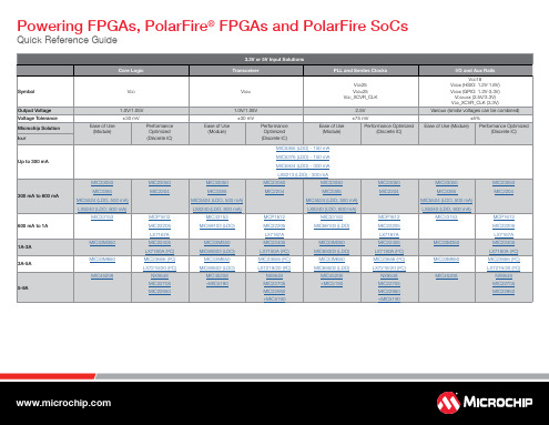
3.3V or 5V Input Solutions
I/O and Aux Rails
Ease of Use (Module)
Performance Optimized (Discrete IC)
MIC45404 MIC45116 MIC45208
MIC24046 (I²C) NX9548 NX9548
MCP1612 MIC22205 LX7167A MIC22405 LX7180A (I²C)
MIC33050 MIC3385 MIC5524 (LDO, 500 mA) LX8240 (LDO, 800 mA) MIC33153 MIC69103 (LDO)
MIC33M350 MIC69303 (LDO)
MIC5365 (LDO) - 150 mA
MIC5376 (LDO) - 150 mA MIC5504 (LDO) - 300 mA LX8213 (LDO) - 300 mA
MIC23050
MIC33050
MIC2204
MIC3385
MIC5524 (LDO, 500 mA) LX8240 (LDO, 800 mA)
Various (similar voltages can be combined)
±5%
Ease of Use (Module)
Performance Optimized (Discrete IC)
MIC33050 MIC3385 MIC5524 (LDO, 500 mA) LX8240 (LDO, 800 mA) MIC33153 MIC69103 (LDO)
600 mA to 1A 1A-3A 3A-5A
5-8A
Core Logic
SureFire 超紧凑LED手枪灯XC1-B用户手册说明书

MOUNTING XC1 TO A HANDGUN
XC1’s rail-mount bolt should be sufficiently loose before sliding the XC1 onto the rail (Fig. 1). To further loosen, if needed, turn screw on rail-mount bolt counterclockwise with a 3/32” Allen wrench until there’s sufficient clearance to slide the XC1 onto the rail and over the cross member. Once properly positioned (looking through the indexing cutout) tighten screw (clockwise) so the bolt rises into the locking notch thereby securing the light to the firearm.
All performance claims tested to ANSI/NEMA FL1-2009 Standard. *runtime and output will be reduced when using a lithium or alkaline battery
USER MANUAL
KIT CONTENTS:
NOTE: If the XC1-B is initially activated to constant on using the slide switch it can only be turned off by moving the slide switch to the OFF position. The toggle switches cannot override the slide switch when it is moved to the ON position.
- 1、下载文档前请自行甄别文档内容的完整性,平台不提供额外的编辑、内容补充、找答案等附加服务。
- 2、"仅部分预览"的文档,不可在线预览部分如存在完整性等问题,可反馈申请退款(可完整预览的文档不适用该条件!)。
- 3、如文档侵犯您的权益,请联系客服反馈,我们会尽快为您处理(人工客服工作时间:9:00-18:30)。
■GENERAL DESCRIPTION The XC9110/9111 series is a group of PFM controlled step-up DC/DC converter/controller ICs designed to generate low supply voltage by the combination of PFM control and CMOS structure. The series is ideal for applications where a longer battery life is needed such as in portable communication equipment. With abuilt-in 2.5ΩN-channel driver transistor, the XC9110A/C/E and XC9111A/C/E types provide a step-up operation by using only acoil, a capacitor, and a diode connected externally.The XC9110/9111B, D and F versions can be used with an external transistor for applications requiring larger currents.Output voltage is internally programmable in a range from 1.5V to 7.0V in increments of 100mV (accuracy:±2.5%). Maximum oscillation frequency is set to 100kHz for XC9110/9111series. (At light loads, it is set to 180kHz for the XC9111 series.) Options include products equipped with a CE pin (Cand D versions) that allows the IC to be shut down thereby reducing supply current and with separated V DD /V OUT pins (E and F versions) to separate the power supply block and the output voltage detect block. With the XC9110 series,maximum duty cycle is set to 75% (V DD =3.3V) making itsuitable for use with large current operations. The XC9111 series automatically switches duty ratio between 56% & 75% (V DD =3.3V) when it senses changes in load to drop output ripple voltage and can support both large and small currents. The external transistor types (B/D/F types) can be provided for applications, which require larger currents .◆Maximum Duty Cycle75% :XC9110 Series 56%/75% Variable :XC9111 Series◆Operating Voltage Range :0.9V ~ 10.0V◆Output Voltage Range :1.5V ~ 7.0V ◆Output Voltage Accuracy :±2.5% ◆Low Supply Current :2.0μA (When operating, V OUT =3V) ◆Built-In Transistor Type :XC9110 / XC9111A*/ C/ E Series ◆External Transistor Type:XC9110 / XC9111B*/ D/ F Series * A and B types are only for the XC9111 series. ■APPLICATIONS●Mobile phones ●Various palm top equipment ●Cameras, VCRs ●Various portable equipment ■FEATURESOperating (Input) Voltage Range : 0.9V ~ 10.0V Output Voltage Range :1.5V~7.0V (100mV increments,accuracy ±2.5%) Maximum Oscillation Frequency :100kHz (accuracy ±15%)180kHz (for the XC9111 series,duty ratio: 56% at light loads) Built-in Switching N-ch Transistor : A/C/E typeON Resistance 2.5Ω (V DD =3.0V) External Transistor Types : B/D/F type Small Package : SOT-23 & SOT89 (for XC9111 series),SOT-25, USP-6C Lx Limit Voltage: E type: more than V DD =2.0V : A/C type: more than V OUT =2.0V ■TYPICAL APPLICATION CIRCUIT■TYPICAL PERFORMANCE CHARACTERISTICS●C type circuitXC9111E331MRL=100μH(CR54), CL47μF(Tantalum)SD: XB01SB04A2BR2/34XC9110/9111Series●XC9111A/BPIN NUMBERSOT-23 SOT-89A B A BPIN NAME FUNCTIONS 1 1 1 1 V SS : Ground 3 3 2 2 V OUT : Output Voltage Montior, Internal Power Supply 2 - 3 - LX : Switch - 2 - 3 EXT : External Switching transistor drive <N-ch transistor drive)●XC9110//9111C/D/E/FPIN NUMBERSOT-25USP-6CC D E F C D E FPIN NAMEFUNCTIONS- - 2 2 - - 1 1 V DD Internal Power Supply4 4 4 4 6 6 6 6 V SS Ground- 5 - 5 - 4 - 4 EXTExternal switching transistor drive<Connect to the gate pin of N-ch Power MOSFET>5 - 5 - 4 - 4- Lx Switch1 1 - - 3 3 --CEChip Enable <Connect to the V OUT pin when Active and theV SS pin when stand-by>2 2 1 1 1 13 3 V OUT Output voltage monitor 3 3 3 3 2,5 2,5 2,5 2,5NC No connection■PIN CONFIGURATIONSOT-25 (TOP VIEW)USP-6C (BOTTOM VIEW)*The dissipation pad for the USP-6C package should be solder-plated in recommended mount pattern and metal masking so as to enhance mounting strength and heat release. If the pad needs to be connected to other pins, it should be connected to the pin No.1.■PIN ASSIGNMENTCE/VOUT 12354VSSVOUT/VDD Lx/EXTNCSOT-23 (TOP VIEW) SOT-89 (TOP VIEW)3/34XC9110/9111SeriesDESIGNATORDESCRIPTIONSYMBOLDESCRIPTIONA : V DD / V OUT common type (for XC9111series) Built-in TransistorB : V DD / V OUT common type (for XC9111series) External TransistorC : CE pin (5 pin) Built-in TransistorD : CE pin (5 pin) External Transistor E : V DD / V OUT separated type (5 pin) Built-in Transistor ① CE FunctionF : V DD / V OUT separated type (5 pin) External Transistor②③ Output Voltage 15 ~ 70 : ex. 3.5V output → ②= 3, ③= 5④Maximum OscillationFrequency1 : 100kHz : SOT-23 (for A and B types)M: SOT-25 (for C, D, F types) P : SOT-89 (for A and B types) ⑤ PackageE : USP-6C (for C, D,F types) R : Embossed tape, standard feed ⑥Device OrientationL: Embossed tape, reverse feed■PRODUCT CLASSIFICATION●Selection Guide ●Ordering InformationXC9110①②③④⑤⑥ : PFM control, 75% dutyXC9111①②③④⑤⑥ : PFM control, 56% / 75% duty variable4/34XC9110/9111Series■PACKAGING INFORMATION●USP-6C●SOT-25 (SOT-23-5)●SOT-23●SOT-895/34XC9110/9111SeriesMARKOUTPUT VOLTAGEFOSC=100kHz1.x 12.x 23.x 34.x 45.x 56.x 67.x 7MARKOUTPUT VOLTAGEFOSC=100KHzx.0 0x.1 1x.2 2x.3 3x.4 4x.5 5x.6 6x.7 7x.8 8x.9 9■ MARKING RULE●SOT-23①Represents product series②Represents integer of output voltage and oscillation frequency④Represents production lot number 0 to 9, A to Z repeated (G, I, J, O, Q, W excepted)6/34XC9110/9111 SeriesMARKOUTPUT VOLTAGEFOSC=100kHz1.x 12.x 23.x 34.x 45.x 56.x 67.x 7MARK OUTPUT VOLTAGEFOSC=100kHzx.0 0 x.1 1 x.2 2 x.3 3 x.4 4 x.5 5 x.6 6 x.7 7 x.8 8 x.9 9■ MARKING RULE (Continued)①Represents product series②Represents integer of output voltage and oscillation frequency●SOT-25③Represents decimal point of output voltage and oscillation frequency④Represents production lot number 0 to 9, A to Z repeated (G, I, J, O, Q, W excepted)SOT-25 (TOP VIEW)7/34XC9110/9111SeriesMARKOUTPUT VOLTAGEFOSC 100kHz1.x 12.x 23.x 34.x 45.x 56.x 67.x 7MARK OUTPUT VOLTAGEFOSC 100kHzx.0 0 x.1 1 x.2 2 x.3 3 x.4 4 x.5 5 x.6 6 x.7 7 x.8 8 x.9 9■ MARKING RULE (Continued)①Represents product series②Represents integer of output voltage and oscillation frequency③Represents decimal point of output voltage and oscillation frequency④Represents production lot number 0 to 9, A to Z repeated (G, I, J, O, Q, W excepted)●SOT-898/34XC9110/9111 SeriesMARKPRODUCT SERIESM XC9110xxx1DxN XC9111xxx1DxMARK FUNCTION PRODUCT SERIESC CE Tr. Built-in XC911xCxx1DxD CE External Tr. XC911xDxx1Dx E V DD /V OUT Tr. Built-in XC911xExx1DxF V DD /V OUT External Tr. XC911xFxx1DxMARKOUTPUT VOLTAGE1 1.x2 2.x3 3.x4 4.x5 5.x6 6.x7 7.xMARKOUTPUT VOLTAGE0 x.0 1 x.1 2 x.2 3 x.3 4 x.4 5 x.56 x.67 x.78 x.89 x.9MARKOSCILLATION FREQUENCYPRODUCT SERIES1 x.0XC911xxxx1Dx①Represents product series②Represents series type●USP-6C ③Represents integer of output voltage④Represents decimal point of output voltage⑥Represents production lot number0 to 9, A to Z repeated (G, I, J, O, Q, W excepted) * No character inversion used⑤Represents oscillation frequencyUSP-6C (TOP VIEW)■ MARKING RULE (Continued)9/34XC9110/9111Series■BLOCK DIAGRAMS●XC9111 A and B seriesNote: The XC9110 series, Tr. Built-in type, uses the Lx pin and the XC9111 series, external Tr. Type, uses the EXT pin.The duty ratio of the XC9111 series automatically varies between 56% (oscillation frequency 180kHz) and 75% (oscillation frequency (FOSC) 100kHz). The V Lx limit function only applies to the XC9110/9111 A types.* The duty ratio depends on power supply. Please refer to the electrical characteristics on duty against output voltage you use.●XC9110 / 9111 C and D seriesNote: The XC9110 series, Tr. Built-in type, uses the Lx pin and the XC9111 series, external Tr. Type, uses the EXT pin.The XC9110 series' duty ratio is 75% and oscillation frequency (FOSC) is 100kHz. The duty ratio of the XC9111 series automatically varies between 56% (oscillation frequency 180kHz) and 75% (oscillation frequency (FOSC) 100kHz). The V Lx limit function only applies to the XC9110/9111 C versions.* The duty ratio depends on power supply. Please refer to the electrical characteristics on duty against output voltage you use.10/34XC9110/9111 SeriesNote: The XC9110 series, Tr. Built-in type, uses the Lx pin and the XC9111 series, external Tr. Type, uses the EXT pin.The XC9110 / 9111 series E and F series have the V DD pin. The XC9110 series' duty ratio is 75% and oscillation frequency (FOSC) is 100kHz. The duty ratio of the XC9111 series automatically varies between 56% (oscillation frequency 180kHz) and 75% (oscillation frequency (FOSC) 100kHz). The V Lx limit function only applies to the XC9110/9111 C versions. * The duty ratio depends on power supply.Please refer to the electrical characteristics on duty against output voltage you use.PARAMETER SYMBOL RATINGS UNITS V OUT Input Voltage V OUT – 0.3 ~ 12.0 V Lx Pin Voltage V Lx – 0.3 ~ 12.0VLx Pin Current I Lx 400 mAEXT Pin Voltage V EXT V SS – 0.3 ~ V OUT +0.3 VEXT Pin Current I EXT ±100 mACE Input Voltage V CE – 0.3 ~ 12.0 V V DD Input VoltageV DD– 0.3 ~ 12.0VSOT-23, 25250 SOT-89 500 Power DissipationUSP-6CPd 100 mW Operating Temperature Range Topr – 40 ~ + 85℃Storage Temperature RangeTstg – 55 ~ +125 ℃ ■ ABSOLUTE MAXIMUM RATINGSTa = 25℃SS ■BLOCK DIAGRAMS●XC9111 E and F seriesSeries ■ELECTRICAL CHARACTERISTICSTa = 25℃Test condition : Unless otherwise specified, V IN=V OUT×0.6, I OUT=<C1(*)>, Vpull=5.0VNOTE:*1: TOREX SBD, XB01SB04A2BR is used, reverse current IR < 1μA (when reverse voltage V R = 10V is applied), in case of using selected parts.*2: Supply Current 1 is the value when the IC is constantly switching. In actual operation, the oscillator periodically switches, resulting in lower power consumption. Please refer to Input Current (I IN) under no load condition for the actual current, which is supplied from the input power supply (V IN).*3: Lx switch ON resistance can be calculated by (V Lx x Rp) / (Vpull - V Lx). * Change Vpull so that V Lx will become 0.4V.*4: The Lx limit voltage function becomes stable when V OUT is over 2.0V.*5: EFFI={[output voltage]×(output current)} / [(input voltage)×(input current)]×100*6: Please be aware of the absolute maximum ratings of the external components.(*): Please refer to the charts.■ELECTRICAL CHARACTERISTICS (Continued)Ta = 25℃Test condition : Unless otherwise specified, V IN=V OUT×0.6, I OUT=<C1(*)>NOTE:*1: Supply Current 1 is the value when the IC is constantly switching. In actual operation, the oscillator periodically switches, resulting in lower power consumption.*2: EXT ‘H’ ON resistance can be calculated by (0.4 x Rp) / ( V EXT – Vpull). * Change Vpull so that V EXT will become V OUT-0.4V.*3: EXT ‘L’ ON resistance can be calculated by (V EXT x Rp) / ( Vpull- V EXT). * Change Vpull so that V EXT will become 0.4V.*4: EFFI={[output voltage]×(output current)} / [(input voltage)×(input current)]×100*5: Please be aware of the absolute maximum ratings of the external components.(*): Please refer to the charts.Series ■ELECTRICAL CHARACTERISTICS (Continued)Ta = 25℃Test condition : Unless otherwise specified, connect CE to V OUT, V IN=V OUT×0.6, I OUT=<C1(*)>, Vpull=5.0VNOTE:*1: TOREX SD, XB01SB04A2BR is used, reverse current IR < 1μA (when reverse voltage V R = 10V is applied), in case of using selected parts.*2: Supply Current 1 is the value when the IC is constantly switching. In actual operation, the oscillator periodically switches, resulting in lower power consumption. Please refer to Input Current (I IN) under no load condition for the actual current, which is supplied from the input power supply (V IN).*3: Lx switch ON resistance can be calculated by (V Lx x Rp) / (Vpull - V Lx). * Change Vpull so that V Lx will become 0.4V.*4: The Lx. limit voltage function becomes stable when V OUT of the XC9110/9111 series is over 2.0V.*5: EFFI={[output voltage]×(output current)} / [(input voltage)×(input current)]×100*6: Please be aware of the absolute maximum ratings of the external components.(*): Please refer to the charts.■ELECTRICAL CHARACTERISTICS (Continued)Ta = 25℃Test condition : Unless otherwise specified, connect CE to V OUT, V IN=V OUT×0.6, I OUT=<C1(*)>NOTE:*1: "Supply Current 1" is the value when the IC is constantly switching. In actual operation, the oscillator periodically switches, resulting in lower power consumption.*2: EXT H ON resistance can be calculated by (0.4 x Rp) / (V EXT - Vpull). * Change Vpull so that V EXT will become V OUT-0.4V.*3: EXT L ON resistance can be calculated by (V EXT x Rp) / (Vpull - V EXT). * Change Vpull so that V EXT will become 0.4V.*4: EFFI={[output voltage]×(output current)} / [(input voltage)×(input current)]×100*5: Please be aware of the absolute maximum ratings of the external components.(*): Please refer to the charts.Series ■ELECTRICAL CHARACTERISTICS (Continued)Test condition : Unless otherwise specified, connect V DD to V OUT, V IN=V OUT×0.6, I OUT=<C1(*)>, Vpull=5.0VNOTE:*1: TOREX SD, XB01SB04A2BR is used; reverse current IR < 1μA (when reverse voltage V R = 10V is applied), in case of using selected parts.*2: "Supply Current 1" is the value when the IC is constantly switching. In actual operation, the oscillator periodically switches, resulting in lower power consumption. Please refer to Input Current (I IN) under no load condition for the actual current, which is supplied from the input power supply (V IN).*3: Lx switch ON resistance can be calculated by (V Lx x Rp) / (Vpull - V Lx). * Change Vpull so that V Lx will become 0.4V.*4: The Lx limit voltage function becomes stable when V OUT of the XC9110/9111 series is over 2.0V.*5: EFFI={[output voltage]×(output current)} / [(input voltage)×(input current)]×100*6: When using V DD and V OUT separately, please set the voltage range of V DD from 1.5V to 10V.The IC operates from V DD=0.8V, but output voltage and oscillation frequency will be stable when V DD=1.5V or more.*7: Please be aware of the absolute maximum ratings of the external components.(*): Please refer to the charts.■ELECTRICAL CHARACTERISTICS (Continued)Ta = 25℃Test condition : Unless otherwise specified, connect V DD to V OUT, V IN=V OUT×0.6, I OUT=<C1(*)>NOTE:*1: "Supply Current 1" is the value when the IC is constantly switching. In actual operation, the oscillator periodically switches, resulting in lower power consumption.*2: EXT H ON resistance can be calculated by (0.4 x Rp) / (V EXT - Vpull). * Change Vpull so that V EXT will become V OUT-0.4V.*3: EXT L ON resistance can be calculated by (V EXT x Rp) / (Vpull - V EXT). * Change Vpull so that V EXT will become 0.4V.*4: EFFI={[output voltage]×(output current)} / [(input voltage)×(input current)]×100*5: When using V DD and V OUT separately, please set the voltage range of V DD from 1.5V to 10V.The IC operates from V DD=0.8V, but output voltage and oscillation frequency will be stable when V DD=1.5V or more.*6: Please be aware of the absolute maximum ratings of the external components.(*): Please refer to the charts.SeriesSYMBOLE2-1E2-2E1-1 E1-2E3-1E3-2E4-1E4-2E5-1 E5-2 E6-1E6-2PARAMETER Supply Current 1 Input Current (No Load) Supply Current 2Lx Switch ON Resistance EXT H ON Resistance EXT LON ResistanceUNIT (μA) (μA) (μA) (Ω) (Ω) (Ω)I DD1 I IN I DD2 R SWON R EXTH R EXTL SETTINGVOLTAGE TYP . MAX.TYP . MAX.TYP .MAX.TYP .MAX.TYP . MAX. TYP .MAX.1.5 7.7 15.1 1.6 8.0 15.61.7 8.3 16.21.8 8.6 16.8 4.2 6.3 160 240 67 1011.9 8.9 17.53.5 2.0 9.3 18.24.3 8.6 1.93.9 3.5 5.3 108 162 52 782.1 9.7 18.92.2 10.1 19.72.3 10.5 20.64.4 8.8 4.0 2.4 11.0 21.52.5 11.5 22.53.24.8 91 137 45 68 2.6 12.0 23.5 4.5 9.1 2.04.1 2.7 12.5 24.5 2.8 13.1 25.62.9 13.7 26.83.0 14.3 28.04.6 9.3 4.2 3.1 15.0 29.32.8 4.2 70 105 38 573.2 15.7 30.63.3 16.4 31.94.7 9.5 2.1 4.3 3.4 17.1 33.33.5 17.8 34.83.6 18.6 36.34.8 9.7 4.4 3.7 19.4 37.93.8 20.3 39.53.9 21.1 41.14.0 22.0 42.85.0 10.0 2.2 4.54.1 22.9 44.54.2 23.8 46.34.3 24.8 48.25.1 10.2 4.6 4.4 25.7 50.04.5 26.7 52.04.6 27.7 53.95.2 10.4 2.34.7 4.7 28.8 56.0 4.8 29.8 58.04.9 30.9 60.15.0 31.7 63.45.3 10.6 4.85.1 32.3 64.75.2 32.9 65.92.53.8 59 89 33 50 5.3 33.5 67.1 5.4 10.8 2.44.95.4 34.1 68.35.5 34.7 69.55.6 35.3 70.75.5 11.1 5.0 5.7 36.0 72.05.8 36.5 73.15.9 37.1 74.36.0 37.7 75.5 5.6 11.3 2.5 5.16.1 38.4 76.86.2 38.9 77.96.3 39.5 79.15.7 11.5 5.26.4 40.2 80.46.5 40.8 81.66.6 41.3 82.7 5.8 11.7 2.65.36.7 42.0 84.0 6.8 42.6 85.26.9 43.2 86.47.0 43.7 87.5 6.0 12.0 2.7 5.42.13.2 40 60 24 36■ELECTRICAL CHARACTERSTICS (Continued)● I DD2, R EXTH , R EXTL , DTY ChartSYMBOL C1 E7-1E7-2 E7-3E8E9EFFICIENCY PARAMETEROUTPUT CURRENT DUTY RATIOXC9110XC9111 XC9110XC9111UNIT (mA)(%)(%) DTY EFFI SETTINGVOLTAGE I OUTMIN. TYP . MAX.TYP .1.5 7.5 1.6 8.01.7 8.51.8 9.0 1.9 9.5 60 75 60 752.0 10.0 2.1 10.5 2.2 11.0 2.3 11.5 2.4 12.02.5 12.5 2.6 13.0 2.7 13.5 2.8 14.0 2.9 14.5 65 79 61 753.0 30.0 3.1 31.0 3.2 32.03.3 33.03.4 34.03.5 35.0 3.6 36.0 3.7 37.0 3.8 38.0 3.9 39.0 77 82 77 824.0 40.0 4.1 41.0 4.2 42.0 4.3 43.0 4.4 44.04.5 45.0 4.6 46.0 4.7 47.0 4.8 48.0 4.9 49.0 80 86 80 835.0 50.0 5.1 51.0 70 75 80 5.2 52.0 5.3 53.0 5.4 54.0 5.5 55.0 5.6 56.0 5.7 57.0 5.8 58.0 5.9 59.06.0 60.06.1 61.06.2 62.0 6.3 63.0 6.4 64.0 6.5 65.0 6.6 66.0 6.7 67.0 6.8 68.0 6.9 69.0 7.0 70.068 73 78 82 88 82 85 ■ELECTRICAL CHARACTERSTICS (Continued)● I OUT , DTY , EFFI ChartSeriesL: 100μH(Coil, CR54, SUMIDA) L: 47μH (Coil, CR54, SUMIDA)SD: XB01SB04A2BR (Schottky type, TOREX) SD: XB01SB04A2BR (Schottky type, TOREX) CL: 16V, 47μF (Tantalum) CL: 16V, 47μF (Tantalum) CIN: 16V, 47μF (Tantalum) CIN: 16V, 47μF (Tantalum) RB: 500Ω CB: 2200pF Tr: 2SD1628■TYPICAL APPLICATION CIRCUITS●C type circuit ●D type circuit●E type circuit●F type circuitL: 100μH (Coil, CR54,SUMIDA)SD: XB01SB04A2BR (Schottky type, TOREX) C L : 16V, 47μF (Tantalum)C IN : 16V,47μF (Tantalum) L: 47μH (Coil, CR54,SUMIDA)SD: XB01SB04A2BR (Schottky type, TOREX) C L : 16V, 47μF (Tantalum)C IN : 16V,47μF (Tantalum) R B : 500Ω C B : 2200pF Tr: 2SD1628 (SANYO)L: 100μH (Coil, CR54,SUMIDA)SD: XB01SB04A2BR (Schottky type, TOREX) C L : 16V, 47μF (Tantalum) C IN : 16V, 47μF (Tantalum)L: 47μH (Coil, CR54,SUMIDA)SD: XB01SB04A2BR (Schottky type, TOREX)C L : 16V,47μF (Tantalum) C IN : 16V, 47μF (Tantalum) R B : 1k Ω C B : 3300pF Tr: 2SD1628 (SANYO)●A type circuit●B type circuit■OPERATIONAL EXPLANATIONThe XC9110/9111 series are PFM controlled step-up DC/DC converter (A, C and E types) / controller ICs (B, D and F types), which contain voltage reference source, PFM comparator, duty selector, PFM controlled OSC, VLx Limiter, driver transistor and so on. With the XC9110 series, maximum duty ratio is set to 75% (maximum oscillation frequency=MAXFOSC: 100kHz) making it suitable for use with large current operations. The XC9111 series automatically switches duty ratio between 56% (MAXFOSC: 180kHz) and 75% (MAXFOSC: 100kHz) when it senses changes in load and can support both large and small currents.<Reference Voltage Source (Vref) >The reference voltage source provides the reference voltage to ensure stable output voltage of the DC/DC converter.< PFM Comparator >The PFM comparator compares the feedback voltage divided by the internal split resistors with the internal reference voltage. When the feedback voltage is higher than the reference voltage, PFM controlled OSC will be stopped. When the feedback voltage is lower than the reference voltage, the PFM controlled OSC will be operated so that the output voltage will be stable by sending a signal to the buffer drive circuit and controlling the internal or external driver transistor. < Duty Selector >With the XC9111 series, the duty selector automatically switches duty ratio between 56% and 75% when it senses changes in load and can support both large and small currents.< PFM Controlled Oscillator >The PFM controlled OSC determines maximum oscillation frequency. The circuit generates the oscillation frequency of 100kHz at 75% duty and 180kHz at 56%.< V Lx Limiter>The V Lx circuit of the XC9110/9111 A, C and D types detects in-rush current and overcurrent, which flows from the V OUT pin to the Lx pin during short-circuit. In overcurrent, the driver transistor will be OFF. When the overcurrent state is eliminated, the IC resumes its normal operation.<Chip Enable Function>The chip enable function of the XC9110/9111 C and D types enables the IC to be in shut down mode when a low level signal is input to the CE pin. During the shut down mode, the current consumption will be reduced to 0.5μA (MAX.).<Separated V DD/V OUT>With the separated V DD pin, the XC9110/9111 E and F types can be operated in both low and high voltage.SeriesV OUT (V) I OUT (mA) V IN (V) R B (Ω) V OUT (V) I OUT (mA) V IN (V) R B (Ω)1.8 10 1.2 4.5 3.3 5 1.2 6.5 1.8 10 1.5 6.0 3.3 5 1.5 6.5 1.8 30 1.22.03.3 10 1.2 5.0 1.8 30 1.5 2.0 3.3 10 1.54.5 1.8 50 1.2 1.2 3.3 30 1.2 3.5 1.8 50 1.5 1.5 3.3 30 1.5 3.5■EXTERNAL COMPONENTSTr.: *Using a MOSFETXP151A13A0MR (N-ch Power MOSFET, TOREX)Note : V GS breakdown voltage of this Transistor is 8V so please be careful with the power supply voltage.If the power supply voltage is over 6V, Please use the XP151A12A2MR with a V GS breakdown voltage of 12V.* Using a NPN Transistor 2SD1628 (SANYO)R B : 500Ω (Adjust in accordance with load and Tr’s hFE.) C B : 2200pF (Ceramic)C B ≦1 / ( 2TT x R B x FOSC x 0.7 )■NOTES ON USE1. Please do not exceed the value of stated absolute maximum ratings.2. The DC/DC converter / controller IC's performance is greatly influenced by not only the ICs' characteristics, but also by those of the external components. Care must be taken when selecting the external components.3. The Lx limit voltage function becomes stable when V OUT of the XC9110/9111C series is over 2.0V and the V DD of the XC9110/9111E series is over 2.0V.4. Make sure that the PCB GND traces are as thick as possible, as variations in ground potential caused by high ground currents at the time of switching may result in instability of the IC.5. Please mount each external component as close to the IC as possible and use thick, short connecting traces to reduce the circuit impedance.●R B value example (when using NPN Transistor)SD: XP01SB04A2BR (TOREX) MA2Q735 (MATSUSHITA) C L : 16V,47μF (Tantalum type, KYOCERA TAJ) C IN : 16V, 47μF (Tantalum type, KYOCERA TAJ) 16V, 220μF (Electrolytic Capacitor) L: <XC9110/9111A, C and E series (Transistor built-in)> <XC9110/9111B, D and F series(Transistor external)>100μH (CR54,SUMIDA) 22μH, 47μH (CR54, SUMIDA)100μH (CDRH6D28,SUMIDA)* Tr.: 2SD1628■TEST CIRCUITSCircuit ④Cp: 100μF (OS-CON, SANYO)Circuit ⑥C IN : 47μF, 16V(Tantalum) L: CR54, 100μH (SUMIDA) Tr: 2SD1628 (SANYO) C B : 2200pF R B : 500ΩSD: XB01SB04A2BR (Schottky , TOREX)C L : 47μF, 16V(Tantalum) Circuit ①C IN : 47μF, 16V (Tantalum) L: CR54, 100μH (SUMIDA) SD: XB01SB04A2BR (Schottky, TOREX)C L : 47μF, 16V(Tantalum)Circuit ② Rp: 300Ω Rp: 10Ω (For Lx ON Resistanceand measuring Lx Limit Current)Rp: 200Ω(For measuring EXT ON Resistance) Cp: 100μF (OS-CON, SANYO)Circuit ①Circuit ② Circuit ③ Circuit ④ Circuit ⑤Circuit ⑥Circuit ⑦Circuit ⑧<External Components>Series■TYPICAL PERFORMANCE CHARACTERISTICS(1) Output Voltage vs. Output Current *Topr = 25℃■TYPICAL PERFORMANCE CHARACTERISTICS (Continued)(1) Output Voltage vs. Output Current (Continued) *Topr = 25℃Series■TYPICAL PERFORMANCE CHARACTERISTICS (Continued)(2) Efficiency vs. Output Current *Topr = 25℃■TYPICAL PERFORMANCE CHARACTERISTICS (Continued)(2) Efficiency vs. Output Current (Continued) *Topr = 25℃Series■TYPICAL PERFORMANCE CHARACTERISTICS (Continued)(3) Ripple Voltage vs. Output Current *Topr = 25℃■TYPICAL PERFORMANCE CHARACTERISTICS (Continued)(3) Ripple Voltage vs. Output Current (Continued) *Topr = 25℃Series ■TYPICAL PERFORMANCE CHARACTERISTICS (Continued)*Topr = 25℃(4) Supply Current 1 vs. Output Voltage (5) Supply Current 2 vs. Output Voltage(6) Stand-by Current vs. Output Voltage (7) No Load Input Current vs. Output Voltage(8) Lx Limit Voltage vs. Output Voltage (9) Lx Switch-ON Resistance vs. Output Voltage* The reason for the increase in the "no load input current" figure at Ta=85℃in the performance characteristics isbecause of an increase in the reverse current of the Schottky diode and not because of abnormalities of the ICitself.■TYPICAL PERFORMANCE CHARACTERISTICS (Continued)*Topr = 25℃(10) EXT H ON Resistance vs. Output Voltage (11) EXT L ON Resistance vs. Output Voltage(12) Maximum Oscillation Frequency 1. vs. Output Voltage (13) Maximum Oscillation Frequency 2 vs. Output Voltage(14) Duty Ratio 1 vs. Output Voltage (15) Duty Ratio 2 vs. Output Voltage■TYPICAL PERFORMANCE CHARACTERISTICS (Continued)*Topr = 25℃(16) Output Voltage vs. Ambient Temperature (17) CE “H”, “L” Voltage vs. Output Voltage(18) Operation Start Voltage vs. Ambient T emperature (19) Oscillation Start Voltage vs. Ambient T emperature(20) Operation Hold Voltage vs. Ambient Temperature■TYPICAL PERFORMANCE CHARACTERISTICS (Continued)(21) Load Transient Response *Topr = 25℃VIN=2.4V, VDD=VOUT, IOUT=0.1mA 50mA■TYPICAL PERFORMANCE CHARACTERISTICS (Continued)(22) Input Transient Response *Topr = 25℃。