EM644FV16FU中文资料
EM621FT16GS-70S中文资料(List Unclassifed)中文数据手册「EasyDatasheet - 矽搜」
CS0.2V,LB0.2V或/和UB0.2V, VIN INV CC -0.2V
周期时间=最小,I IO=0毫安,100%关税, CS=V IL, LB=V IL 或/和UB = V IL , VIN=VIL 或V IH
平均工作电流
ICC2
输出低电压 输出高电压 待机电流(TTL)
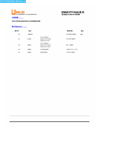
从生产代码变化
年1月18个,2007年
0.2 0.3 0.4
0.2版本 0.3版本 0.4版本
EM681FV16U-45LF至 EM681FV16AU-45LF
产品代码表更新 修正错字错误
四月.
10,2007
二零零七年六月十五日
11月12个,2007年
芯片中文手册,看全文,戳
EM681FV16AU系列
2.2
-
mA V V mA
V OL V OH ISB
IOL = 2.1mA IOH = -1.0mA CS=V IH,其他输入= V CSV
CC-0.2V CC CC=3.3V @ 25 CC=3.6V @ 85 IH 或V IL
-
待机电流(CMOS)
ISB1
其他输入= 0〜V (典型值条件:V (最大条件:V
(V cc = 2.7至3.6V,GND = 0V,T
符号
A
= -40 o C至+ 85 o C)
55ns 70ns Max 55 55 35 55 5 5 5 0 0 0 10 A 20 20 20 5 5 5 0 0 0 10 Min 70 Max 70 70 35 70 25 25 25 Min 55 -
.
电容
1)
(f =1MHz, T A =25 o C)
EM643FV16FU中文资料
Document Title256K x16 bit Super Low Power and Low Voltage Full CMOS Static RAMRevision HistoryRevision No. History Draft Date Remark0.0Initial Draft May 26 , 2003 Preliminary0.12’nd Draft Add Pb-free part number February 13 , 2004Emerging Memory & Logic Solutions Inc.IT Venture Tower Eastside 11F, 78, Karac-Dong, Songpa-Ku, Seoul, Rep.of Korea Zip Code : 138-160Tel : +82-2-2142-1759~1766 Fax : +82-2-2142-1769 / Homepage : The attached datasheets are provided by EMLSI reserve the right to change the specifications and products. EMLSI will answer to your questions about device. If you have any questions, please contact the EMLSI office.FEATURES•Process Technology : 0.18µm Full CMOS •Organization : 256K x 16 bit•Power Supply Voltage : 2.7V ~ 3.6V •Low Data Retention Voltage : 1.5V(Min.)•Three state output and TTL Compatible •Package Type : 44-TSOP2GENERAL DESCRIPTIONThe EM643FV16FU families are fabricated by EMLSI’s advanced full CMOS process technology. The families support industrial temperature range and Chip Scale Package for user flexibility of system design. The fami-lies also supports low data retention voltage for battery back-up operation with low data retention current.PRODUCT FAMILYProduct FamilyOperating TemperatureVcc Range SpeedPower DissipationPKG TypeStandby (I SB1, Typ.) Operating (I CC1.Max.) EM643FV16FU Industrial (-40 ~ 85o C)2.7V~3.6V551) /70ns1 µA 2)3 mA44-TSOP2Name FunctionName FunctionCS Chip select input Vcc Power Supply O E Output Enable input Vss GroundWE Write Enable input UB Upper Byte (I/O 9~16)A 0~A 17Address InputsLBLower Byte (I/O 1~8)I/O 1~I/O 16 Data Inputs/outputsNC No ConnectionR o w S e l e c tI/O Circuit Column SelectData Cont Data ContPre-charge CircuitMemory Array 2048 x 2048A 1A 2A 3A 4A 5A 6A 7A 0A 8A 9A 11A 12A 13A 14A 15A 16A 17W EO E U BLB C SI/O1 ~ I/O8I/O9 ~ I/O16V C CV SSControl LogicFUNCTIONAL BLOCK DIAGRAM1. The parameter is measured with 30pF test load.A 10PIN DESCRIPTION 1234567891011121314151644434241403938373635343332313029A4A3A2A1A0C S I/O1I/O2I/O3I/O4VCC VSS I/O5I/O6I/O7I/O8A5A6A7OE UB LB I/O16I/O15I/O14I/O13VSS V C C I/O12I/O11I/O10I/O944 - TSOP2171819202122282726252423WE A17A16A15A14A13NC A8A9A10A11A122. Typical values are measured at Vcc=3.3V, T A =25o C and not 100% tested.ABSOLUTE MAXIMUM RATINGS *Parameter Symbol Ratings Unit Voltage on Any Pin Relative to Vss V IN, V OUT-0.2 to Vcc+0.3(Max.4.0V)V Voltage on Vcc supply relative to Vss V CC-0.2 to 4.0V V Power Dissipation P D 1.0W Operating Temperature T A-40 to 85o C*Stresses greater than those listed under “Absolute Maximum Ratings” may cause permanent damage to the device. Functional operation should be restricted to recommended operating condition. Exposure to absolute maximum rating conditions for extended periods may affect reliability.FUNCTIONAL DESCRIPTIONCS OE WE LB UB I/O1-8I/O9-16Mode PowerH X X X X High-Z High-Z Deselected Stand byL H H X X High-Z High-Z Output Disabled ActiveL X X H H High-Z High-Z Output Disabled ActiveL L H L H Data Out High-Z Lower Byte Read ActiveL L H H L High-Z Data Out Upper Byte Read ActiveL L H L L Data Out Data Out Word Read ActiveL X L L H Data In High-Z Lower Byte Write ActiveL X L H L High-Z Data In Upper Byte Write ActiveL X L L L Data in Data In Word Write ActiveNote: X means don’t care. (Must be low or high state)DC AND OPERATING CHARACTERISTICSNOTES1. Typical values are measured at Vcc=3.3V, T A =25o C and not 100% tested.ParameterSymbol Test Conditions Min Typ Max Unit Input leakage current I LI V IN =V SS to V CC-1-1µA Output leakage current I LO CS=V IH or OE=V IH or WE=V IL , V IO =V SS to V CC -1-1µA Operating power supplyI CC I IO =0mA, CS=V IL , V IN =V IH or V IL --3mA Average operating currentI CC1Cycle time=1µs, 100% duty, I IO =0mA, CS<0.2V, V IN <0.2V or V IN >V CC -0.2V --3mAI CC2Cycle time = Min, I IO =0mA, 100% duty, CS=V IL, V IN =V IL or V IH 55ns --30mA 70ns--25 Output low voltage V OL I OL = 2.1mA --0.4V Output high voltage V OH I OH = -1.0mA2.4--V Standby Current (TTL)I SB CS=V IH , Other inputs=V IH or V IL --0.3mAStandby Current (CMOS)I SB1CS>V CC -0.2V, Other inputs=0~V CC(Typ. condition : V CC =3.3V @ 25o C)(Max. condition : V CC =3.6V @ 85o C)LL LF-11)12µARECOMMENDED DC OPERATING CONDITIONS 1)1. TA= -40 to 85o C, otherwise specified2. Overshoot: V CC +2.0 V in case of pulse width < 20ns3. Undershoot: -2.0 V in case of pulse width < 20ns4. Overshoot and undershoot are sampled, not 100% tested .ParameterSymbol Min Typ Max Unit Supply voltage V CC 2.7 3.3 3.6V GroundV SS 000V Input high voltage V IH 2.2-V CC + 0.22)V Input low voltageV IL-0.23)-0.6VCAPACITANCE 1) (f =1MHz, T A =25o C)1. Capacitance is sampled, not 100% testedItemSymbol Test ConditionMin Max Unit Input capacitance C IN V IN =0V -8pF Input/Ouput capacitanceC IOV IO =0V-10pFEM643FV16FU SeriesLow Power, 256Kx16 SRAMmerging Memory & Logic Solutions Inc.ParameterSymbol55ns 70nsUnitMin Max Min Max Read cycle time t RC 55-70-ns Address access time t AA -55-70ns Chip select to outputt CO -55-70ns Output enable to valid output t OE -25-35ns UB, LB acess time t BA 25 35ns Chip select to low-Z output t LZ 10-10-ns UB, LB enable to low-Z output t BLZ 5- 5 -ns Output enable to low-Z output t OLZ 5-5-ns Chip disable to high-Z output t HZ 020025ns UB, LB disable to high-Z output t BHZ 020025ns Output disable to high-Z output t OHZ 020025ns Output hold from address changet OH10-10-nsParameterSymbol55ns 70nsUnitMin Max Min Max Write cycle timet WC 55-70-ns Chip select to end of write t CW 45-60-ns Address setup timet AS 0-0-ns Address valid to end of write t AW 45-60-ns UB, LB valid to end of write t BW 45-60-ns Write pulse width t WP 40-55-ns Write recovery time t WR 0-0-ns Write to ouput high-Z t WHZ 020025ns Data to write time overlap t DW 25 30 ns Data hold from write time t DH 0-0-ns End write to output low-Zt OW5-5-nsREAD CYCLE (V cc =2.7 to 3.6V, Gnd = 0V, T A = -40o C to +85o C)WRITE CYCLE (V cc =2.7 to 3.6V, Gnd = 0V, T A = -40o C to +85o C)AC OPERATING CONDITIONSTest Conditions (Test Load and Test Input/Output Reference)Input Pulse Level : 0.4 to 2.2V Input Rise and Fall Time : 5nsInput and Output reference Voltage : 1.5V Output Load (See right) : CL = 100pF+ 1 TTL CL 1) = 30pF + 1 TTL 1. Including scope and Jig capacitance 2. R 1=3070Ω, R 2=3150Ω3. V TM =2.8VCL 1)V TM 3)R 12)R 22)t AddressCSUB,LBOEData Outt COt OHt B At O EHigh-ZTIMING WAVEFORM OF READ CYCLE(2) (WE = V IH )Data ValidOLZt t LZAAHZt RCAddresst AA Data Validt OHPrevious Data ValidTIMING WAVEFORM OF READ CYCLE(1). IL IH, or/and =V IL )Data OutTIMING DIAGRAMSNOTES (READ CYCLE)1. t HZ and t OHZ are defined as the outputs achieve the open circuit conditions and are not referanced to output voltage levels.2. At any given temperature and voltage condition, t HZ (Max.) is less than t LZ (Min.) both for a given device and from device to device interconnection.WR (4)t WC AddressCS UB,LB WE Data in Data outt CW(2)t AWt BWt WP(1)t AS(3)High-Zt DW t DHHigh-Zt OWt WHZData UndefinedTIMING WAVEFORM OF WRITE CYCLE(1) (WE CONTROLLED)Data Validt WCAddressCS UB,LB WE Data in Data outt CW(2)t WR(4)t AWt BWt WP(1)t DW t DHTIMING WAVEFORM OF WRITE CYCLE(2) (CS CONTROLLED)tAS(3)High-Z High-ZData Validt AddressCSUB,LBWEData in Data outt CW (2)W R (4)t A W t B Wt W P (1)t DWDHTIMING WAVEFORM OF WRITE CYCLE(3) (UB, LB CONTROLLED)High-ZHigh-ZData ValidA S NOTES (WRITE CYCLE)1. A write occurs during the overlap(t WP ) of low CS and low WE. A write begins when CS goes low and WE goes low with asserting UB or LB for single byte operation or simultaneously asserting UB and LB for double byte operation. A write ends at the earliest transition when CS goes high and WE goes high. The t WP is measured from the beginning of write to the end of write.2. t CW is measured from the CS going low to end of write.3. t AS is measured from the address valid to the beginning of write.4. t WR is measured from the end or write to the address change. t WR applied in case a write ends as CS or WE going high.DATA RETENTION CHARACTERISTICSNOTES 1. See the I SB1 measurement condition of datasheet page 4.2. Typical values are measured at T A =25o C and not 100% tested.ParameterSymbolTest ConditionMinTyp 2)MaxUnitV CC for Data Retention V DR I SB1 Test Condition (Chip Disabled) 1)1.5- 3.6V Data Retention CurrentI DR V CC =1.5V, I SB1 Test Condition(Chip Disabled) 1)-0.5-µAChip Deselect to Data Retention Time t SDR See data retention wave form0--nsOperation Recovery Time t RDRt RC--V cc 2.7V2.2V V DRCS GNDDATA RETENTION WAVE FORMUnit: millimeters PACKAGE DIMENSIONEM643FV16FU SeriesLow Power, 256Kx16 SRAMmerging Memory & Logic Solutions Inc.1. EMLSI Memory2. Device Type3. Density 5. Technology 8. Version 9. Packages 10. Speed7. Orgainzation1. Memory Component2. Device Type6 ------------------------ Low Power SRAM7 ------------------------ STRAM 3. Density1 ------------------------- 1M2 ------------------------- 2M 4 ------------------------- 4M 8 ------------------------- 8M 16 ----------------------- 16M 32 ----------------------- 32M 64 ----------------------- 64M4. Mode Option 0 -------- Dual CS 1 -------- Single CS2 -------- Multiplexed Address3 -------- Single CS with LB,UB (tBA=tOE)4 -------- Single CS with LB,UB (tBA=tCO)5 -------- Dual CS with LB,UB (tBA=tOE)6 -------- Dual CS with LB,UB (tBA=tCO)5. TechnologyBlank ------------------ CMOSF ------------------------ Full CMOS 6. Operating Voltage Blank ------------------- 5VV ------------------------- 2.7V~3.6V U ------------------------- 3.0V S ------------------------- 2.5V R ------------------------- 2.0V P ------------------------- 1.8V4. Option 11. Power 7. Orginzation8 ---------------------- x8 bit 16 ---------------------- x16 bit 32 ---------------------- x32 bit8. VersionBlank ----------------- Mother Die A ----------------------- First revision B ----------------------- Second revision C ----------------------- Third revision D ----------------------- Fourth revision E ----------------------- Fifth revision F ----------------------- Sixth revision 9. PackageBlank ---------------------- FPBGAS ---------------------------- 32 sTSOP1 T ---------------------------- 32 TSOP1 U ---------------------------- 44 TSOP2 W ---------------------------- Wafer10. Speed45 ---------------------- 45ns 55 ---------------------- 55ns 70 ---------------------- 70ns 85 ---------------------- 85ns 10 --------------------- 100ns 12 --------------------- 120ns11. PowerLL ---------------------- Low Low PowerLF ---------------------- Low Low Power (Pb-free) L ---------------------- Low PowerS ---------------------- Standard Power元器件交易网。
Cineroid EVF4RVW 电子查看器说明书

Thank you for purchasing the Cineroid EVF.The Cineroid EVF (hereafter referred to as “EVF") is a view finder that can be mounted on any video camera with a HDMI output signal. Please thoroughly read the user manual for best operation and understanding of all of the functions of the EVF.Test Before OperatingIt is recommended to test the EVF before operating. Check if the EVF can be turned on once powered, and check if the information/menu is being properly displayed on the LCD.Copyrights and ProhibitionsThe use of images of people, property, and places can without permission can be prohibited by law. Please refer to your region’s laws regarding copyrights.02○ Canon and EOS are registered trademarks of Canon.○ Nikon is a registered trademark of Nikon.○ Sony is a registered trademark of Sony.○ Panasonic is a registered trademark of Panasonic.1. Do not face the eyecup directly into the sun as it may damage the LCD.2. The shadow disk is installed on EVF at factory. This shadow disk can be removed by disassembling eyecup from loupe.EnglishSafety Precautions◎ Do not use any batteries, power cord, or accessories that are not specified in this document.◎ When using a power cord, be sure to plug it in completely. Do not handle power plugswhen your hands are wet. When unplugging the power cord, grasp the plug body or adapter instead of the cord.◎ Power cords that are scratched, heavily bent or twisted can potentially be hazardous and a source of electric shock and/or fire.◎ Do not insert foreign objects into the product’s electric or cable components.◎ Do not place the power cord near sources of heat as this may melt or cause damage to the cord potentially causing fire or electric shock.◎ Do not disassemble or modify the product. This may damage the product and cause danger due to a malfunction.◎ Please keep the product out of reach of young children. Injuries may occur due to damage to the product.◎ When using the product in an airplane or hospital setting, it is recommended to acquireauthorization first as signals or electro-magnetic waves from the product may cause other equipment to malfunction.◎ Do not store the product in a dusty or humid environment as damage may occur.◎ When the product is mounted on a camera, do not lift or move the camera by grabbing the product. This may cause damage to the product or the camera mount.◎ Do not clean the product with paint thinner, benzene, or other volatile solvents. This may cause damage to the product and become a fire hazard.◎ This product is not waterproof. If the product is dropped in water, contact the servicecenter immediately.Please observe the following safety precautions as they are meant for the safe and proper use of the product to reduce the risk of accidents. Upon reading the user manual, keep it in a safe and available place.03Table of ContentsSafety PrecautionsTable of ContentsComponentsPartsBefore Using the EVFOpenable Optical LoupeHood for LoupeSeparate of LoupeAdjusting the Diopter / Connecting Extention Tube Installing the BatteryConnecting External PowerConnecting input / outputPower On/OffBasic FeaturesOperating the MenuAdjusting ColorAdjusting the ScreenVolume Control 03 04 06 07 08 08 09 09 10 10 11 1112 13 13 1304EnglishShooting Features Peaking Pixel to Pixel Clip guideWaveform / Vectorscope False color 1 False color 2 Monochrome Look up table FreezeOver Scaling Underscan Crop Guide Anamorphic Center Marker Time Code Screen FlipSetting User Controls Custom Button Functions Firmware UpgradeCustom Display Settings Parameter Save And Restore Factory ResetProduct Specifications Optional Products051415151617172020212518212323251919242418222224ComponentsPlease ensure all parts are present after opening the box.06EnglishParts 0708Openable Optical LoupeHood for LoupeThe optical loupe attached to the EVF body can beflipped open 180 degrees.English09Separate of Loupecompletely.When viewing through the optical loupe, the user can adjust the diopter accordingly. Rotate the dial in either direction until the image becomes clear. and Extention tube is used toextend loupe length for old eye.Adjusting the Diopter / Connecting Extension tube1 Touch Removealbe10Connecting External PowerDC in 6~17VProper voltage for external power is 6-17V.Attention to the connecting polarities and voltage, otherwise the connectors may be damaged.When both external power and battery is connected, battery is not consumed.Before Using the EVF Connecting input / outputOperating the Menu3. to access that feature.EnglishPeakingOn/Off : Menu - Control1 - Peaking Setting : Menu - Setting1 - PeakingPeaking Red ONPeaking Red OFF Peaking On / OffPeaking SettingTo activate the peaking feature, simply press the F1 button on the left side of theEVF body. The peaking will show in the mode that is currently selected.Simple Peaking Button*Peaking Sharpness OFF Peaking Sharpness ONEnglishPixel to pixelOn/Off : Menu - Control1 - Pixel to PixelPixel to Pixel Off Pixel to Pixel OnPixel to Pixel Off Clip GuideOn/Off : Menu - Control1 - Clip Guide Setting : Menu - Setting1 - Clip GuideClip Guide Off Clip Guide Color mode Clip Guide Zebra modeClip Guide On / Off Clip Guide SettingPixel to Pixel OnWaveform / VectorscopeOn/Off : Menu - Control1 - Waveform Setting : Menu - Setting1 - WaveformStyle 1. Only horizontal waveform withimage croppingWaveform OFFStyle 2. Horizontal and vertical waveform with small vectorscope Style 3. Horizontal and vertical waveform with big vectorscopeWaveform On / OffWaveform Setting T o c h a n g e t h e w a v e f o r m s t y l e,s i m p l y s c r o l lthe wheel button on the left side of the cineroidE V F4R V W's b o d y.T h e w a v e f o r m s t y l e w i l ls h o w i n t h e m o d e t h a t i s c u r r e n t l y s e l e c t e d.Simple change waveform style*False Color2 Off False Color2 OnLook up tableOn/Off : Menu - Control1 - Look up tableLook up table Off(The image applied adjusting color)Look up table OffLook up table On(Original image)Monochrome (B /W, Blue, Red, Green)On/Off : Menu - Control1 - Monochrome Setting : Menu - Setting1 - MonochromeMonochrome On / Off Monochrome SettingMonochrome (B/W) OffMonochrome (B/W) OnFreezeOn/Off : Menu - Control1 - FreezeEnglish Freeze Off Freeze OnFreeze Off Freeze OnCrop guideOn/Off : Menu - Control2 - Crop Guide Setting : Menu - Setting1 - Crop GuideCrop guide Off Crop guide OnCrop guide On / Off Crop guide SettingUnderscanOn/Off : Menu - Control2 - UnderscanUnderscan Off Underscan OnUnderscan Off Underscan OnEnglish21Shooting FeaturesCenter MarkerOn/Off : Menu - Control2 - Center MarkerCenter Marker Off Center Marker Off Center Marker OnCenter Marker OnAnamorphicOn/Off : Menu - Control2 - Anamorphic Setting : Menu - Setting1 - AnamorphicAnamorphic Off Anamorphic OnAnamorphic On / Off Anamorphic SettingTime CodeOn/Off : Menu - Control2 - Time CodeTime code Off Time Code OnTime Code On / Off Time Code Setting22TC 01:22:34EnglishCustom Button FunctionsSetting : Menu - Setting2 - Key AllocationThe left side of the EVF body contains the buttons F1, F2, F3, F4. The factory default forFirmware Upgrade1. Firmware is upgradable by special cable.2. Connect EVF and computer by cable.3. Select On of Firmware Upgrade. The screen is changed to waiting message.4. EVF starts firmware upgrade.Setting User ControlsControl1 Control2 Setting1 Setting2 System ExitF1-Back / Exit Firmware Upgrade set V01.03Input Select Parameter Save Parameter Restore Firmware Exit Upgrade Cancel23Setting User ControlsCustom Display SettingsSetting : Menu - Setting1 - AnamorphicYou can select to view the current state of the battery usage, volume, etc. on the LCD.Factory reset1. Powering on the EVF while pressing down the F1 button will reset the EVF to its original default settings.2. Once the reset is complete, fully power off the EVF before powering on for further use.Parameter save and restoreSetting : Menu - System - Parameter Save/RestoreThe all parameters of function can be stored on bank0 or bank1. The parameters can be restored from bank0 or bank1. Factory is the initial parameter of factory.Parameter Save Parameter Restore24Peaking ONOSD Pixel to Pixel ONEnglishProduct Specifications25Optional Product2627Seculine Co., LTD.Tel +82.70.4347.4901 / Fax +82.2.850.3027Rm.510, Kolon Science Valley #2, Guro-dong, 811, Guro-gu, Seoul, 152-728, Korea Homepage E-mail *******************Printed in KoreaEVF1.0We will strive to create the best products andprovide superb service.。
得捷电子 MT 系列微开关MT系列微小开关数据表说明书

MICRO SWITCH Miniature Toggle SwitchesMT SeriesDESCRIPTIONHoneywell MICRO SWITCH MT Series miniature toggle switches are designed to meet the need for a rugged, cost-effective toggle switch. Quality construction features include a seal between the toggle lever and bushing, and between the cover and case. These switches are designed for use inapplications in many demanding outdoor environments, where the panels are subjected to such things as vibration fromequipment, temperature extremes, dust, splashing water, and/or hose directed water.They are capable of withstanding exposure to heavyaccumulations of early morning dew that may condense on the control panel in cabs of vehicles left outdoors overnight. The MT toggle switches with metal or plastic levers are well suited for gloved-hand operation.The panel stand-off with O-ring feature available on some listings eliminates the need for behind-the-panel hardware, provides a uniform panel height, and a panel-to-cover seal.VALUE TO CUSTOMERS• Spring-loaded mechanism provides enhanced tactile feedback for toggle switch lever• High sealing level and electrical life cycle enable more uptime in field installations which helps in keeping machines working longer with less downtime• Small size allows for smaller control box/panel size to reduce weight and operator fatigueFEATURES• Miniature behind-panel size (case) enables overall control box or panel use• IEC 60529-2001, IP67, IP68 (except terminal parts) sealing for harsh-duty applications• Up to 60,000 electrical life that enhances the use time • Available with 8 circuitry options• 2- or 3- position maintained and momentary action to meet circuit and actuator requirements• UL recognized, CE certified for global usePOTENTIAL APPLICATIONSRemote control box of • Concrete pumping • Cranes• Material handling • Boom trucks• Any application with small panel constraintsDIFFERENTIATION• 60K life cycle offers an enhanced application life, keeping maintenance, replacement, and refurbishment at a minimum• High seal rating (IP68) to protect the toggle from water ingress and support more equipment uptimePORTFOLIOHoneywell offers an extensive line of MICRO SWITCH toggle switches, including the following Series: TL , NT , TW , TS , AT , and ET .Sensing and Internet of Things005437Issue 12 * These positions are momentary. All others are maintained.Sensing and Internet of Things 34 Figure 1. DImensions mm [in]2-Pole Switch7,291-Pole SwitchFigure 2. Panel CutoutPanel Cut-out005437-1-EN IL50 GLO December 2016© 2016 Honeywell International Inc. All rights reserved.m WARNINGPERSONAL INJURYDO NOT USE these products as safety or emergency stop devices or in any other application where failure of the product could result in personal injury.Failure to comply with these instructions could result in death or serious injury.m WARNINGMISUSE OF DOCUMENTATION• The information presented in this product sheet is for reference only. Do not use this document as a product installation guide.•Complete installation, operation, and maintenanceinformation is provided in the instructions supplied with each product.Failure to comply with these instructions could result in death or serious injury.Find out moreHoneywell serves its customers through a worldwide network of sales offices, representatives and distributors. For application as-sistance, current specifications, pricing or name of the nearest Authorized Distributor, contact your local sales office.To learn more about Honeywell’s sensing and switching products, call +1-815-235-6847 or 1-800-537-6945,visit , or e-mail inquiries to *********************ADDITIONAL MATERIALSThe following associated literature is available on the Honeywell web site at :• Product installation instructions • Product range guide• Product application-specific informationHoneywell Sensing and Internet of Things 9680 Old Bailes Road Fort Mill, SC 29707 Warranty/RemedyHoneywell warrants goods of its manufacture as being free of defective materials and faulty workmanship during the appli-cable warranty period. Honeywell’s standard product warranty applies unless agreed to otherwise by Honeywell in writing; please refer to your order acknowledgement or consult your local sales office for specific warranty details. If warrantedgoods are returned to Honeywell during the period of coverage, Honeywell will repair or replace, at its option, without charge those items that Honeywell, in its sole discretion, finds defec-tive. The foregoing is buyer’s sole remedy and is in lieu of all other warranties, expressed or implied, including those of merchantability and fitness for a particular purpose. In no event shall Honeywell be liable for consequential, special, or indirect damages.While Honeywell may provide application assistance personally, through our literature and the Honeywell web site, it is buyer’s sole responsibility to determine the suitability of the product in the application.Specifications may change without notice. The information we supply is believed to be accurate and reliable as of this writing. However, Honeywell assumes no responsibility for its use.。
EM643FV16F系列256K x16位低功耗低电压全CMOS静态RAM产品说明书

Document Title256K x16 bit Super Low Power and Low Voltage Full CMOS Static RAMRevision HistoryRevision No. History Date Remark0.0-.Initial Draft May262003Preliminary0.1-.Add Pb-free part number Feb.1320040.2-.I SB1(Max.) changed from 12uA to 6uA.Mar.3120080.3-.Add 45ns part specification.Apr.22009-.I SB1(Typ.) changed from 1uA to 0.25uA.-.I SB1(Max.) changed from 6uA to 4uA.-.Memory Function Guide updated in the last page.Apr.72009Release1.0-.EM643FV16F(KGD), EM643FV16F series & EM643FV16FUseries are unified to EM643FV16F Family.Emerging Memory & Logic Solutions Inc.3F Korea Construction Financial Cooperative B/D, 301-1 Yeon-Dong, Jeju-Si, Jeju-Do, Rep.of Korea Zip Code : 690-717Tel : +82-64-740-1700 Fax : +82-64-740-1750 / Homepage : The attached datasheets are provided by EMLSI reserve the right to change the specifications and products. EMLSI will answer to your questions about device. If you have any questions, please contact the EMLSI office.PRODUCT FAMILY1. “xx” represents speed.2. Typical values are measured at Vcc=3.3V, T A =25o C and not 100% tested.Product FamilyOperating Temperature Vcc RangeSpeedPower DissipationPKG Type Standby (I SB1, Typ.)Operating (I CC1.Max.)EM643FV16F Industrial (-40 ~ 85o C)2.7 ~3.6 V 45/55/70 ns0.25 µA 2)3 mAKGDEM643FV16F - xx 1)LF VFBGA-48 EM643FV16FU - xx 1)LF44-TSOP2FEATURES•Process Technology : 0.18µm Full CMOS •Organization : 256K x 16 bit•Power Supply Voltage : 2.7V ~ 3.6V •Low Data Retention Voltage : 1.5V(Min.)•Three state output and TTL Compatible •Package Type : VFBGA-48, 44-TSOP2GENERAL DESCRIPTIONThe EM643FV16F families are fabricated by EMLSI’s advanced full CMOS process technology. The families support industrial temperature range and Chip Scale Package for user flexibility of system design. The families also supports low data retention voltage for battery back-up operation with low data retention current.R o w S e l e c tI/O Circuit Column SelectData ContData ContPre-charge CircuitMemory Array 2048 x 2048A1A2A3A4A5A6A7A0A8A9A11A12A13A14A15A16A17WE OE UB LB CSDQ0 ~ DQ7DQ8 ~ DQ15VCCVSSControl LogicA10FUNCTIONAL BLOCK DIAGRAMPIN DESCRIPTIONName FunctionName FunctionCS Chip Select input VCC Power Supply OE Output Enable input VSS GroundWE Write Enable input UB Upper Byte (DQ8~DQ15)A0~A17 Address inputs LB Lower Byte (DQ0~DQ7)DQ0~DQ15Data inputs/outputsNCNo ConnectionPIN CONFIGURATIONSVFBGA-48 : Top view(ball down)123456A LB OE A0A1A2NC B DQ8UB A3A4CS DQ0C DQ9DQ10A5A6DQ1DQ2D VSS DQ11A17A7DQ3VCCE VCC DQ12 NC A16DQ4VSSF DQ14DQ13A14A15DQ5DQ6G DQ15NC A12A13WE DQ7HNCA8A9A10A11NC1234567891011121314151644434241403938373635343332313029A4A3A2A1A0CS DQ0DQ1DQ2DQ3VCC VSS DQ4DQ5DQ6DQ7A5A6A7OE UB LB DQ15DQ14DQ13DQ12VSS VCC DQ11DQ10DQ9DQ844 - TSOP2171819202122282726252423WE A17A16A15A14A13NC A8A9A10A11A1244 - TSOP2 : Top viewABSOLUTE MAXIMUM RATINGS 1)1. Stresses greater than those listed under “Absolute Maximum Ratings” may cause permanent damage to the device. Functional operation should be restricted to recommended operating condition. Exposure to absolute maximum rating conditions for extended periods may affect reliability.FUNCTIONAL DESCRIPTIONNOTE : X means don’t care. (Must be low or high state)ParameterSymbol Ratings Unit Voltage on Any Pin Relative to Vss V IN , V OUT-0.2 to 4.0V Voltage on Vcc supply relative to Vss V CC -0.2 to 4.0V Power Dissipation P D 1.0WOperating TemperatureT A-40 to 85oCCS OE WE LB UB DQ0~7DQ8~15Mode Power H X X X X High-Z High-Z Deselected Stand by X X X H H High-Z High-Z Deselected Stand by L H H L X High-Z High-Z Output Disabled Active L H H X L High-Z High-Z Output Disabled Active L L H L H Data Out High-Z Lower Byte Read Active L L H H L High-Z Data Out Upper Byte Read Active L L H L L Data Out Data Out Word Read Active L X L L H Data In High-Z Lower Byte Write Active L X L H L High-Z Data In Upper Byte Write Active LXLLLData InData InWord WriteActiveRECOMMENDED DC OPERATING CONDITIONS 1)1. TA= -40 to 85o C, otherwise specified2. Overshoot: VCC +2.0 V in case of pulse width < 20ns3. Undershoot: -2.0 V in case of pulse width < 20ns4. Overshoot and undershoot are sampled, not 100% tested.CAPACITANCE 1) (f =1MHz, T A =25o C)1. Capacitance is sampled, not 100% tested.DC AND OPERATING CHARACTERISTICS1. Typical values are measured at Vcc=3.3V, T A =25o C and not 100% tested.ParameterSymbol Min Typ Max Unit Supply voltage V CC 2.7 3.3 3.6V GroundV SS 000V Input high voltage V IH 2.2 -V CC + 0.22)V Input low voltageV IL-0.23)-0.6VItemSymbol Test ConditionMin Max Unit Input capacitance C IN V IN =0V -8pF Input/Ouput capacitanceC IOV IO =0V-10pFParameterSymbol Test Conditions Min Typ Max Unit Input leakage current I LI V IN =V SS to V CC-1-1µA Output leakage current I LO CS=V IH or OE=V IH or WE=V IL or LB=UB=V IH V IO =V SS to V CC-1-1µA Operating power supplyI CC I IO =0mA, CS=V IL , V IN =V IH or V IL --3mA Average operating currentI CC1Cycle time=1µs, 100% duty, I IO =0mA, CS<0.2V, LB<0.2V or/and UB<0.2V, V IN <0.2V or V IN >V CC -0.2V--3mAI CC2Cycle time = Min, I IO =0mA, 100% duty, CS=V IL , LB=V IL or/and UB=V IL , V IN =V IL or V IH 45ns --35mA55ns --3070ns--25 Output low voltage V OL I OL = 2.1mA--0.4V Output high voltage V OH I OH = -1.0mA2.4--V Standby Current (TTL)I SB CS=V IH , Other inputs=V IH or V IL--0.3mAStandby Current (CMOS)I SB1CS>V CC -0.2V , Other inputs = 0~V CC(Typ. condition : V CC =3.3V @ 25o C) (Max. condition : V CC =3.6V @ 85o C)LL LF-0.25 1)4µAAC OPERATING CONDITIONSTest Conditions (Test Load and Test Input/Output Reference)Input Pulse Level : 0.4 to 2.2V Input Rise and Fall Time : 5nsInput and Output reference Voltage : 1.5VOutput Load (See right) : CL 1) = 100pF+ 1 TTL(70ns) CL 1) = 30pF + 1 TTL(45ns/55ns)1. Including scope and Jig capacitance2. R 1=3070Ω, R 2=3150Ω3. V TM =2.8V4. CL = 5pF + 1 TTL (measurement with tLZ, tOLZ, tHZ, tOHZ, tWHZ)READ CYCLE (V cc =2.7 to 3.6V, Gnd = 0V, T A = -40o C to +85o C)WRITE CYCLE (V cc =2.7 to 3.6V, Gnd = 0V, T A = -40o C to +85o C)ParameterSymbol45ns 55ns70nsUnitMin Max Min Max Min Max Read cycle time t RC 45-55-70-ns Address access time t AA -45-55-70ns Chip select to output t CO -45-55-70ns Output enable to valid output t OE -20-25-35ns UB, LB acess time t BA 20 25 35ns Chip select to low-Z output t LZ 10-10-10-ns UB, LB enable to low-Z output t BLZ 5-5-5-ns Output enable to low-Z output t OLZ 5-5-5-ns Chip disable to high-Z output t HZ 020020025ns UB, LB disable to high-Z output t BHZ 020020025ns Output disable to high-Z output t OHZ 020020025ns Output hold from address changet OH10-10-10-nsParameterSymbol45ns 55ns70nsUnitMin Max Min Max Min Max Write cycle timet WC 45-55-70-ns Chip select to end of write t CW 35-45-60-ns Address setup time t AS 0-0-0-ns Address valid to end of write t AW 35-45-60-ns UB, LB valid to end of write t BW 35-45-60-ns Write pulse width t WP 35-40-55-ns Write recovery time t WR 0-0-0-ns Write to ouput high-Z t WHZ 0202025nsData to write time overlap t DW 25 25 30 ns Data hold from write time t DH 0-0-0-ns End write to output low-Zt OW5-5-5-nsCL 1)V TM 3)R 12)R 22)t RCAddressCSUB,LBOEData Outt COt OHt BAt OEHigh-Zt BHZt OHZTIMING WAVEFORM OF READ CYCLE(2) (WE = V IH )Data Validt OLZt BLZ t LZt AAt HZt RCAddresst AA Data Validt OHPrevious Data ValidTIMING WAVEFORM OF READ CYCLE(1) (Address Controlled, CS=OE=V IL , WE=V IH, UB or/and LB =V IL )Data OutTIMING DIAGRAMSNOTES (READ CYCLE)1. t HZ and t OHZ are defined as the outputs achieve the open circuit conditions and are not referenced to output voltage levels.2. At any given temperature and voltage condition, t HZ (Max.) is less than t LZ (Min.) both for a given device and from device to device interconnection.t WR (4)t WCAddressCSUB,LBWEData inData outt CW (2)t AW t BWt WP (1)t AS (3)High-Zt DWt DHHigh-Z t OWt WHZData UndefinedTIMING WAVEFORM OF WRITE CYCLE(1) (WE Controlled)Data Validt WCAddressCSUB,LBWEData inData outt CW (2)t WR (4)t BWt WP (1)t DWt DHTIMING WAVEFORM OF WRITE CYCLE(2) (CS Controlled)tAS(3)High-Z High-ZData Validt AWt WCAddressCSUB,LBWEData in Data outt CW (2)t WR (4)t BWt WP (1)t DWt DHTIMING WAVEFORM OF WRITE CYCLE(3) (UB, LB Controlled)High-ZHigh-ZData Validt AS (3)NOTES (WRITE CYCLE)1. A write occurs during the overlap(t WP ) of low CS and low WE. A write begins when CS goes low and WE goes low with asserting UB or LB for single byte operation or simultaneously asserting UB and LB for double byte operation. A write ends at the earliest transition when CS goes high and WE goes high. The t WP is measured from the beginning of write to the end of write.2. t CW is measured from the CS going low to end of write.3. t AS is measured from the address valid to the beginning of write.4. t WR is measured from the end or write to the address change. t WR applied in case a write ends as CS or WE going high.t AWDATA RETENTION CHARACTERISTICSNOTES1. See the I SB1 measurement condition of datasheet page 5.2. Typical values are measured at T A =25o C and not 100% tested.ParameterSymbolTest ConditionMinTyp 2)MaxUnitV CC for Data Retention V DR I SB1 Test Condition (Chip Disabled) 1)1.5- 3.6V Data Retention CurrentI DR V CC =1.5V, I SB1 Test Condition (Chip Disabled) 1)-0.5-µAChip Deselect to Data Retention Time t SDR See data retention wave form0--nsOperation Recovery Timet RDRt RC--t SDRt RDRData Retention ModeCS > Vcc-0.2VV cc 2.7V2.2V V DRCS GNDDATA RETENTION WAVE FORMPACKAGE DIMENSION44 - TSOP2 (0.8mm pin pitch)Unit : millimeters / inchesAB CD E F G H654321DVFBGA 48 BALLS (6X7X1 0.75mm ball pitch)M Min.NOR.Max.A ---1A10.220.32A20.21 REF A30.45 REF b 0.32 5.250.42D 6 BSCE 7 BSC e 0.75 BSC D10.35 BSC E15.25 BSCNOTES.1). DIMENSION b IS MEASURED AT THE MAXIMUM SOLDER BALL DIAMETER, PARALLEL TO DATUM PLANE Z.2). DATUM Z (SEATING PLANE) IS DEFINED BY THE SPHERICAL CROWNS OF THE SOLDER BALLS.3). PARALLELISM MESUREMENT SHALL EXCLUDE ANY EFFECT OF MARK ON TOP SURFACE OF PACKAGE.DETAIL KA1 CORNERUnit: millimetersA1 CORNERXE Y0.1 ZE17X ee/2e/25X eD148X b 1)0.15 M Z X Y 0.08 M ZDETAIL KM0.08 ZZ0.1 ZAA1(A2)(A3)SEATING PLANE2)3)MEMORY FUNCTION GUIDE1. Memory Component8. VersionBlank---------------Mother die2. Device Type A ---------------2 nd generation 6---------------Low Power SRAM B ---------------3 rd generation 7---------------STRAM C ---------------4 th generation C ---------------CellularRAM D ---------------5 th generation E ---------------6 th generation3. Density F ---------------7 th generation 1--------------- 1MG ---------------8 th generation 2--------------- 2M 4--------------- 4M 9. Package8--------------- 8M Blank---------------KGD, FBGA 16--------------- 16M S ---------------32 sTSOP132--------------- 32M T ---------------32 TSOP164--------------- 64M U ---------------44 TSOP228---------------128MV ---------------32 SOP 4. Option 10. Speed 0---------------Dual CS (x8)45--------------- 45ns 1---------------Single CS (x8)55--------------- 55ns 3---------------Single CS / tBA=tOE (x16)60--------------- 60ns 4---------------Single CS / tBA=tCO (x16)70--------------- 70ns 5---------------Dual CS / tBA=tOE (x16)85--------------- 85ns 6---------------Dual CS / tBA=tCO (x16)90--------------- 90ns 10---------------100ns 5. Technology 12---------------120nsF ---------------Full CMOS 11. Power 6. Operating Voltage LL ---------------Low Low PowerT ---------------5.0V LF ---------------Low Low Power(Pb-free & Green)V ---------------3.3V L ---------------Low PowerU ---------------3.0V S ---------------Standard PowerS ---------------2.5V R ---------------2.0V P ---------------1.8V 7. Organization 8--------------- X8 bit 16---------------X16 bit 32---------------X32 bitEMX XX XXX XX XX -XX XX1. EMLSI Memory2. Device Type 11. Power3. Density 10. Speed4. Function 9. Package5. Technology 8. Version6. Operating Voltage7. Organization。
MEMORY存储芯片MT46V16M16TG-6TIT K中文规格书

Registers22.3.3.1Frame Done(DONE)When the LCD is disabled by clearing the LCD Raster Control enable bit(RASTER_EN=0)in the LCD Raster Control Register,the LCD allows the current frame to complete before it is disabled.After the last set of pixels is clocked out onto the LCD data pins by the pixel clock,the LCD is disabled and DONE is set.•DONE=1when the frame is complete.•DONE=0as long as the frame is not complete.The frame done(DONE)bit signals the frame is complete.It is cleared when the RASTER_EN bit is set to 1(turned ON).22.3.3.2Frame Synchronization Lost(SYNC)The frame synchronization lost(SYNC)bit is set if the LCD controller detects a frame synchronizationerror.A frame synchronization error can occur for one of two reasons:•when the LCD controller attempts to read what it believes to be the first word of the video buffer but cannot be recognized as such•if the LCD controller is starved of data,which can happen due to insufficient bandwidth from the source of LCD data through the system interconnect to the LCD controllerTo alleviate data bandwidth bottleneck issues to the LCD controller,the following configuration settings can be experimented with:•Increase DDR2/mobile DDR(mDDR)memory controller(if used)Command Re-Ordering(PBBPR) setting from default to a value such as10h to20h•Increase LCD FIFO threshold•Increase priority for LCD controller DMA•Increase burst size setting for LCD controller DMA•Run the DDR2/mobile DDR(mDDR)memory controller(if used)at maximum clock speedThis bit is cleared by disabling the LCD controller(RASTER_EN=0).This also resets the input FIFO in the DMA controller.•SYNC=1when a frame synchronization lost occurred.•SYNC=0as long as no frame synchronization error occurs.22.3.3.3AC-Bias Count Status(ABC)The ac-bias count status(ABC)bit is set each time the ac-bias line transitions a particular number of times as specified by the ac-bias line transitions per interrupt(ACB_I)field in LCD Raster Timing Register2.If ACB_I is programmed with a non-zero value,a counter is loaded with the value in ACB_I and isdecremented each time the ac-bias line reverses state.When the counter reaches zero,the ABC bit is set that signals an interrupt request to the interrupt controller.The counter reloads using the value in ACB_I, but does not start to decrement again until you clear ABC by writing0to the LCD status register.•ABC=1when the ac-bias transition counter ACB_I has decremented to0•ABC=0as long as ACB_I has not decremented to022.3.3.4FIFO Underflow Status(FUF)The FIFO underflow status(FUF)bit is set when the input FIFO is completely empty and the LCD data pins driver logic attempts to fetch data from the FIFO.This bit is cleared by disabling the LCD controller (RASTER_EN=0).To recover from this condition and restart normal function of the LCDC,the peripheral needs to be reset through the Power and Sleep Controller(PSC).•FUF=1when the dithering logic is not supplying data to the FIFO at a sufficient rate.•FUF=0as long as FIFO has not underrun.SPRUH79C–April2013–Revised September2016Submit Documentation FeedbackD a t a l i n e s (f r o m 1 t o L )Data pixels (from 1 to P)ArchitectureSPRUH79C–April 2013–Revised September 2016Submit Documentation Feedback22.2.5.6Subpanel FeatureIn some applications,it is desired to display only the first or last few lines of the LCD panel (see Figure 22-14).This is mainly used for power saving.This is supported by the Raster Controller via its subpanel feature.The RASTER_SUBPANEL register fully defines its behavior,that is,the following parameters are defined:•Whether the first or last few lines will be refreshed.•A line number,which is the last (or first)line to be refreshed.•The pixel data to be loaded to the refresh area.Note that there is only one pixel value for all the pixels in the refresh area.As a result,frame buffers and DMA engine are not used in this case,which leads to power saving.Figure 22-14.Raster Mode Display Format。
VF64变频器参数表

85
F-02
负侧过频率设定
HZ
-85
F-03
过负荷保护设定
%
95
F-14
故障重试次数
0
G-02
模拟量频率设定特性选择
1 0~10V(单极性)
G-03
模拟量频率指令上限频率
%
100
G-04
模拟量频率指令下限频率
%
0
H-00
予置频率指令1
HZ
10
H-01
予置频率指令2
HZ
20
H-02
予置频率指令3
HZ
VF64变频器参数表
序号
设定项目
单位
机载设定值
1.FJoG
正转点动频率
HZ
2
2.RJoG
反转点动频率
HZ
2
3.Acc1
加速时间(1)
sec
15
4.Acc1
加速时间(2)
sec
10
7.tbst
转矩提升量
%
1
A-00
最高频率
HZ
83.4
A-01
最低频率
HZ
1.5
A-02
电动机容量
KW
80
A-03
电动机额定电压
端子台MI1功能选择
0
c-02
端子台MI2功能选择
1
c-03
端子台MI3功能选择
2
E-00
驱动侧转矩限制
%
105
E-01
再生侧转矩限制
%
70
E-02
选择使用驱动侧转矩限制
1 ON(使用)
E-04
v/f曲线选择
MEMORY存储芯片MT46V16M16FG-75IT中文规格书
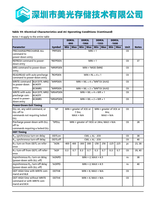
Table 55: Electrical Characteristics and AC Operating Conditions (Continued)Table 55: Electrical Characteristics and AC Operating Conditions (Continued)Notes: 1.AC timing parameters are valid from specified T C MIN to T C MAX values.2.All voltages are referenced to V SS .3.Output timings are only valid for R ON34 output buffer selection.4.The unit t CK (AVG) represents the actual t CK (AVG) of the input clock under operation.The unit CK represents one clock cycle of the input clock, counting the actual clock edges.5.AC timing and I DD tests may use a V IL -to-V IH swing of up to 900mV in the test environ-ment, but input timing is still referenced to V REF (except t IS, t IH, t DS, and t DH use the AC/DC trip points and CK, CK# and DQS, DQS# use their crossing points). The minimum slew rate for the input signals used to test the device is 1 V/ns for single-ended inputs and 2 V/ns for differential inputs in the range between V IL(AC) and V IH(AC).6.All timings that use time-based values (ns, µs, ms) should use t CK (AVG) to determine the correct number of clocks (Table 55 (page 80) uses CK or t CK [AVG] interchangeably). In the case of noninteger results, all minimum limits are to be rounded up to the nearest whole integer, and all maximum limits are to be rounded down to the nearest whole integer.7.Strobe or DQS diff refers to the DQS and DQS# differential crossing point when DQS is the rising edge. Clock or CK refers to the CK and CK# differential crossing point when CK is the rising edge.8.This output load is used for all AC timing (except ODT reference timing) and slew rates.The actual test load may be different. The output signal voltage reference point is V DDQ /2 for single-ended signals and the crossing point for differential signals (see Figure 28 (page 72)).1Gb: x4, x8, x16 DDR3L SDRAM Electrical Characteristics and AC Operating Conditions9.When operating in DLL disable mode, Micron does not warrant compliance with normal mode timings or functionality.10.The clock’s t CK (AVG) is the average clock over any 200 consecutive clocks and t CK (AVG)MIN is the smallest clock rate allowed, with the exception of a deviation due to clock jitter. Input clock jitter is allowed provided it does not exceed values specified and must be of a random Gaussian distribution in nature.11.Spread spectrum is not included in the jitter specification values. However, the inputclock can accommodate spread-spectrum at a sweep rate in the range of 20–60 kHz with an additional 1% of t CK (AVG) as a long-term jitter component; however, the spread spectrum may not use a clock rate below t CK (AVG) MIN.12.The clock’s t CH (AVG) and t CL (AVG) are the average half clock period over any 200 con-secutive clocks and is the smallest clock half period allowed, with the exception of a de-viation due to clock jitter. Input clock jitter is allowed provided it does not exceed values specified and must be of a random Gaussian distribution in nature.13.The period jitter (t JITper) is the maximum deviation in the clock period from the averageor nominal clock. It is allowed in either the positive or negative direction.14.t CH (ABS) is the absolute instantaneous clock high pulse width as measured from onerising edge to the following falling edge.15.t CL (ABS) is the absolute instantaneous clock low pulse width as measured from one fall-ing edge to the following rising edge.16.The cycle-to-cycle jitter t JITcc is the amount the clock period can deviate from one cycleto the next. It is important to keep cycle-to-cycle jitter at a minimum during the DLL locking time.17.The cumulative jitter error t ERRnper, where n is the number of clocks between 2 and 50,is the amount of clock time allowed to accumulate consecutively away from the average clock over n number of clock cycles.18.t DS (base) and t DH (base) values are for a single-ended 1 V/ns slew rate DQs and 2 V/nsslew rate differential DQS, DQS#; when DQ single-ended slew rate is 2V/ns, the DQS dif-ferential slew rate is 4V/ns.19.These parameters are measured from a data signal (DM, DQ0, DQ1, and so forth) transi-tion edge to its respective data strobe signal (DQS, DQS#) crossing.20.The setup and hold times are listed converting the base specification values (to whichderating tables apply) to V REF when the slew rate is 1 V/ns. These values, with a slew rate of 1 V/ns, are for reference only.21.When the device is operated with input clock jitter, this parameter needs to be deratedby the actual t JITper (larger of t JITper (MIN) or t JITper (MAX) of the input clock (output deratings are relative to the SDRAM input clock).22.Single-ended signal parameter.23.The DRAM output timing is aligned to the nominal or average clock. Most output pa-rameters must be derated by the actual jitter error when input clock jitter is present,even when within specification. This results in each parameter becoming larger. The fol-lowing parameters are required to be derated by subtracting t ERR10per (MAX): t DQSCK (MIN), t LZDQS (MIN), t LZDQ (MIN), and t AON (MIN). The following parameters are re-quired to be derated by subtracting t ERR10per (MIN): t DQSCK (MAX), t HZ (MAX), t LZDQS (MAX), t LZDQ MAX, and t AON (MAX). The parameter t RPRE (MIN) is derated by subtract-ing t JITper (MAX), while t RPRE (MAX) is derated by subtracting t JITper (MIN).24.The maximum preamble is bound by t LZDQS (MAX).25.These parameters are measured from a data strobe signal (DQS, DQS#) crossing to its re-spective clock signal (CK, CK#) crossing. The specification values are not affected by the amount of clock jitter applied, as these are relative to the clock signal crossing. These parameters should be met whether clock jitter is present.26.The t DQSCK (DLL_DIS) parameter begins CL + AL - 1 cycles after the READ command.27.The maximum postamble is bound by t HZDQS (MAX).1Gb: x4, x8, x16 DDR3L SDRAM Electrical Characteristics and AC Operating Conditions。
- 1、下载文档前请自行甄别文档内容的完整性,平台不提供额外的编辑、内容补充、找答案等附加服务。
- 2、"仅部分预览"的文档,不可在线预览部分如存在完整性等问题,可反馈申请退款(可完整预览的文档不适用该条件!)。
- 3、如文档侵犯您的权益,请联系客服反馈,我们会尽快为您处理(人工客服工作时间:9:00-18:30)。
Document Title256K x16 bit Super Low Power and Low Voltage Full CMOS Static RAMRevision HistoryRevision No. History Draft Date Remark0.0Initial Draft May 26 , 2003 Preliminary0.12’nd Draft Add Pb-free part number February 13 , 2004Emerging Memory & Logic Solutions Inc.IT Venture Tower Eastside 11F, 78, Karac-Dong, Songpa-Ku, Seoul, Rep.of Korea Zip Code : 138-160Tel : +82-2-2142-1759~1766 Fax : +82-2-2142-1769 / Homepage : The attached datasheets are provided by EMLSI reserve the right to change the specifications and products. EMLSI will answer to your questions about device. If you have any questions, please contact the EMLSI office.FEATURES•Process Technology : 0.18µm Full CMOS •Organization : 256K x 16 bit•Power Supply Voltage : 2.7V ~ 3.6V •Low Data Retention Voltage : 1.5V(Min.)•Three state output and TTL Compatible •Package Type : 44-TSOP2GENERAL DESCRIPTIONThe EM644FV16FU families are fabricated by EMLSI’s advanced full CMOS process technology. The families support industrial temperature range and Chip Scale Package for user flexibility of system design. The fami-lies also supports low data retention voltage for battery back-up operation with low data retention current.PRODUCT FAMILYProduct FamilyOperating TemperatureVcc Range SpeedPower DissipationPKG TypeStandby (I SB1, Typ.) Operating (I CC1.Max.) EM644FV16FU Industrial (-40 ~ 85o C)2.7V~3.6V551) /70ns1 µA 2)3 mA44-TSOP2Name FunctionName FunctionCS Chip select input Vcc Power Supply O E Output Enable input Vss GroundWE Write Enable input UB Upper Byte (I/O 9~16)A 0~A 17Address InputsLBLower Byte (I/O 1~8)I/O 1~I/O 16 Data Inputs/outputsNC No ConnectionR o w S e l e c tI/O Circuit Column SelectData Cont Data ContPre-charge CircuitMemory Array 2048 x 2048A 1A 2A 3A 4A 5A 6A 7A 0A 8A 9A 11A 12A 13A 14A 15A 16A 17W EO E U BLB C SI/O1 ~ I/O8I/O9 ~ I/O16V C CV SSControl LogicFUNCTIONAL BLOCK DIAGRAM1. The parameter is measured with 30pF test load.A 10PIN DESCRIPTION 1234567891011121314151644434241403938373635343332313029A4A3A2A1A0C S I/O1I/O2I/O3I/O4VCC VSS I/O5I/O6I/O7I/O8A5A6A7OE UB LB I/O16I/O15I/O14I/O13VSS V C C I/O12I/O11I/O10I/O944 - TSOP2171819202122282726252423WE A17A16A15A14A13NC A8A9A10A11A122. Typical values are measured at Vcc=3.3V, T A =25o C and not 100% tested.ABSOLUTE MAXIMUM RATINGS *Parameter Symbol Ratings Unit Voltage on Any Pin Relative to Vss V IN, V OUT-0.2 to Vcc+0.3(Max.4.0V)V Voltage on Vcc supply relative to Vss V CC-0.2 to 4.0V V Power Dissipation P D 1.0W Operating Temperature T A-40 to 85o C*Stresses greater than those listed under “Absolute Maximum Ratings” may cause permanent damage to the device. Functional operation should be restricted to recommended operating condition. Exposure to absolute maximum rating conditions for extended periods may affect reliability.FUNCTIONAL DESCRIPTIONCS OE WE LB UB I/O1-8I/O9-16Mode PowerH X X X X High-Z High-Z Deselected Stand byX X X H H High-Z High-Z Deselected Stand byL H H L X High-Z High-Z Output Disabled ActiveL H H X L High-Z High-Z Output Disabled ActiveL L H L H Data Out High-Z Lower Byte Read ActiveL L H H L High-Z Data Out Upper Byte Read ActiveL L H L L Data Out Data Out Word Read ActiveL X L L H Data In High-Z Lower Byte Write ActiveL X L H L High-Z Data In Upper Byte Write ActiveL X L L L Data in Data In Word Write ActiveNote: X means don’t care. (Must be low or high state)DC AND OPERATING CHARACTERISTICSNOTES1. Typical values are measured at Vcc=3.3V, T A =25o C and not 100% tested.ParameterSymbol Test Conditions Min Typ Max Unit Input leakage current I LI V IN =V SS to V CC-1-1µA Output leakage current I LO CS=V IH or OE=V IH or WE=V IL , V IO =V SS to V CC -1-1µA Operating power supplyI CC I IO =0mA, CS=V IL , V IN =V IH or V IL --3mA Average operating currentI CC1Cycle time=1µs, 100% duty, I IO =0mA, CS<0.2V, V IN <0.2V or V IN >V CC -0.2V --3mAI CC2Cycle time = Min, I IO =0mA, 100% duty, CS=V IL, V IN =V IL or V IH 55ns --30mA 70ns--25 Output low voltage V OL I OL = 2.1mA --0.4V Output high voltage V OH I OH = -1.0mA2.4--V Standby Current (TTL)I SB CS=V IH , Other inputs=V IH or V IL --0.3mAStandby Current (CMOS)I SB1CS>V CC -0.2V, Other inputs=0~V CC(Typ. condition : V CC =3.3V @ 25o C)(Max. condition : V CC =3.6V @ 85o C)LL LF-11)12µARECOMMENDED DC OPERATING CONDITIONS 1)1. TA= -40 to 85o C, otherwise specified2. Overshoot: V CC +2.0 V in case of pulse width < 20ns3. Undershoot: -2.0 V in case of pulse width < 20ns4. Overshoot and undershoot are sampled, not 100% tested .ParameterSymbol Min Typ Max Unit Supply voltage V CC 2.7 3.3 3.6V GroundV SS 000V Input high voltage V IH 2.2-V CC + 0.22)V Input low voltageV IL-0.23)-0.6VCAPACITANCE 1) (f =1MHz, T A =25o C)1. Capacitance is sampled, not 100% testedItemSymbol Test ConditionMin Max Unit Input capacitance C IN V IN =0V -8pF Input/Ouput capacitanceC IOV IO =0V-10pFEM644FV16FU SeriesLow Power, 256Kx16 SRAMmerging Memory & Logic Solutions Inc.ParameterSymbol55ns 70nsUnitMin Max Min Max Read cycle time t RC 55-70-ns Address access time t AA -55-70ns Chip select to outputt co -55-70ns Output enable to valid output t OE -25-35ns UB, LB acess time t BA 55 70ns Chip select to low-Z output t LZ 10-10-ns UB, LB enable to low-Z output t BLZ 10- 10 -ns Output enable to low-Z output t OLZ 5-5-ns Chip disable to high-Z output t HZ 020025ns UB, LB disable to high-Z output t BHZ 020025ns Output disable to high-Z output t OHZ 020025ns Output hold from address changet OH10-10-nsParameterSymbol55ns 70nsUnitMin Max Min Max Write cycle timet WC 55-70-ns Chip select to end of write t CW 45-60-ns Address setup timet As 0-0-ns Address valid to end of write t AW 45-60-ns UB, LB valid to end of write t BW 45-60-ns Write pulse width t WP 40-55-ns Write recovery time t WR 0-0-ns Write to ouput high-Z t WHZ 020025ns Data to write time overlap t DW 25 30 ns Data hold from write time t DH 0-0-ns End write to output low-Zt OW5-5-nsREAD CYCLE (V cc =2.7 to 3.6V, Gnd = 0V, T A = -40o C to +85o C)WRITE CYCLE (V cc =2.7 to 3.6V, Gnd = 0V, T A = -40o C to +85o C)AC OPERATING CONDITIONSTest Conditions (Test Load and Test Input/Output Reference)Input Pulse Level : 0.4 to 2.2V Input Rise and Fall Time : 5nsInput and Output reference Voltage : 1.5V Output Load (See right) : CL = 100pF+ 1 TTL CL 1) = 30pF + 1 TTL 1. Including scope and Jig capacitance 2. R 1=3070Ω, R 2=3150Ω3. V TM =2.8VCL 1)V TM 3)R 12)R 22)t AddressCSUB,LBOEData Outt COt OHt B At O EHigh-ZTIMING WAVEFORM OF READ CYCLE(2) (WE = V IH )Data ValidOLZt t LZAAHZt RCAddresst AA Data Validt OHPrevious Data ValidTIMING WAVEFORM OF READ CYCLE(1). IL IH, or/and =V IL )Data OutTIMING DIAGRAMSNOTES (READ CYCLE)1. t HZ and t OHZ are defined as the outputs achieve the open circuit conditions and are not referanced to output voltage levels.2. At any given temperature and voltage condition, t HZ (Max.) is less than t LZ (Min.) both for a given device and from device to device interconnection.WR (4)t WC AddressCS UB,LB WE Data in Data outt CW(2)t AWt BWt WP(1)t AS(3)High-Zt DW t DHHigh-Zt OWt WHZData UndefinedTIMING WAVEFORM OF WRITE CYCLE(1) (WE CONTROLLED)Data Validt WCAddressCS UB,LB WE Data in Data outt CW(2)t WR(4)t AWt BWt WP(1)t DW t DHTIMING WAVEFORM OF WRITE CYCLE(2) (CS CONTROLLED)tAS(3)High-Z High-ZData Validt AddressCSUB,LBWEData in Data outt CW (2)W R (4)t A W t B Wt W P (1)t DWDHTIMING WAVEFORM OF WRITE CYCLE(3) (UB, LB CONTROLLED)High-ZHigh-ZData ValidA S NOTES (WRITE CYCLE)1. A write occurs during the overlap(t WP ) of low CS and low WE. A write begins when CS goes low and WE goes low with asserting UB or LB for single byte operation or simultaneously asserting UB and LB for double byte operation. A write ends at the earliest transition when CS goes high and WE goes high. The t WP is measured from the beginning of write to the end of write.2. t CW is measured from the CS going low to end of write.3. t AS is measured from the address valid to the beginning of write.4. t WR is measured from the end or write to the address change. t WR applied in case a write ends as CS or WE going high.DATA RETENTION CHARACTERISTICSNOTES 1. See the I SB1 measurement condition of datasheet page 4.2. Typical values are measured at T A =25o C and not 100% tested.ParameterSymbolTest ConditionMinTyp 2)MaxUnitV CC for Data Retention V DR I SB1 Test Condition (Chip Disabled) 1)1.5- 3.6V Data Retention CurrentI DR V CC =1.5V, I SB1 Test Condition(Chip Disabled) 1)-0.5-µAChip Deselect to Data Retention Time t SDR See data retention wave form0--nsOperation Recovery Time t RDRt RC--V cc 2.7V2.2V V DRCS GNDDATA RETENTION WAVE FORMUnit: millimeters PACKAGE DIMENSIONEM644FV16FU SeriesLow Power, 256Kx16 SRAMmerging Memory & Logic Solutions Inc.1. EMLSI Memory2. Device Type3. Density 5. Technology 8. Version 9. Packages 10. Speed7. Orgainzation1. Memory Component2. Device Type6 ------------------------ Low Power SRAM7 ------------------------ STRAM 3. Density1 ------------------------- 1M2 ------------------------- 2M 4 ------------------------- 4M 8 ------------------------- 8M 16 ----------------------- 16M 32 ----------------------- 32M 64 ----------------------- 64M4. Mode Option 0 -------- Dual CS 1 -------- Single CS2 -------- Multiplexed Address3 -------- Single CS with LB,UB (tBA=tOE)4 -------- Single CS with LB,UB (tBA=tCO)5 -------- Dual CS with LB,UB (tBA=tOE)6 -------- Dual CS with LB,UB (tBA=tCO)5. TechnologyBlank ------------------ CMOSF ------------------------ Full CMOS 6. Operating Voltage Blank ------------------- 5VV ------------------------- 2.7V~3.6V U ------------------------- 3.0V S ------------------------- 2.5V R ------------------------- 2.0V P ------------------------- 1.8V4. Option 11. Power 7. Orginzation8 ---------------------- x8 bit 16 ---------------------- x16 bit 32 ---------------------- x32 bit8. VersionBlank ----------------- Mother Die A ----------------------- First revision B ----------------------- Second revision C ----------------------- Third revision D ----------------------- Fourth revision E ----------------------- Fifth revision F ----------------------- Sixth revision 9. PackageBlank ---------------------- FPBGAS ---------------------------- 32 sTSOP1 T ---------------------------- 32 TSOP1 U ---------------------------- 44 TSOP2 W ---------------------------- Wafer10. Speed45 ---------------------- 45ns 55 ---------------------- 55ns 70 ---------------------- 70ns 85 ---------------------- 85ns 10 --------------------- 100ns 12 --------------------- 120ns11. PowerLL ---------------------- Low Low PowerLF ---------------------- Low Low Power (Pb-free) L ---------------------- Low PowerS ---------------------- Standard Power元器件交易网。