PI3CH480QE中文资料
爱普生(EPSON)实时时钟模块RA4803SA规格书
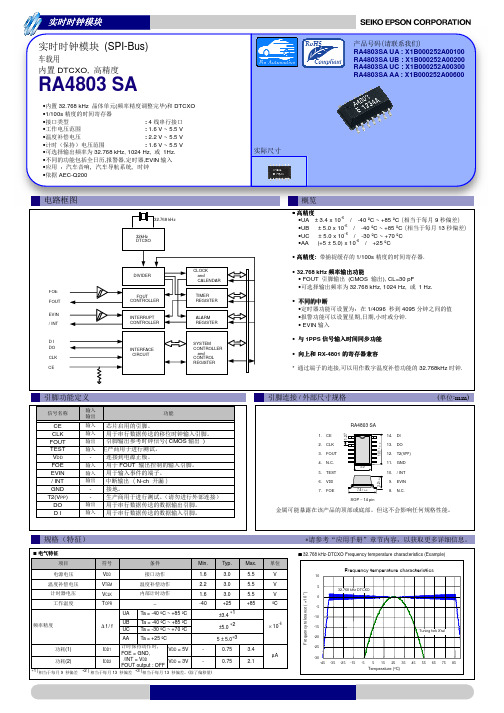
DIVIDER
FOUT CONTROLLER
INTERRUPT CONTROLLER
INTERFACE CIRCUIT
CLOCK and CALENDAR
TIMER REGISTER
ALARM REGISTER
SYSTEM CONTROLLER
and CONTROL REGISTER
• •UA •UB •UC •AA
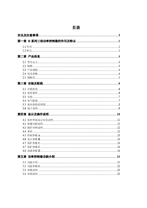
± 3.4 x 10⁻⁶ / -40 ºC ~ +85 ºC 商
± 5.0 x 10⁻⁶ / -40 ºC ~ +85 ºC 商 ± 5.0 x 10⁻⁶ / -30 ºC ~ +70 ºC (+5 ± 5.0) x 10-6 / +25 ºC
9
器
13
器
•
:
1/100s
●为汽车行驶安全方面的应用(引擎控制单元、气囊、电子稳定程序控制系统)。
注意事项
·本材料如有变更,恕不另行通知。量产设计时请确认最新信息。 ·未经 Seiko Epson 公司书面授权,禁止以任何形式或任何方式复制或者发布本材料中任何部分的信息内容。 ·本材料中的书面信息、应用电路、编程、使用等内容仅供参考。Seiko Epson 公司对第三方专利或版权的侵权行为不负有任何责任。本材料
0
-5
-10
-15 Tuning fork X'tal
-20
-25
-30 -45 -35 -25 -15 -5 5 15 25 35 45 55 65 75 85 Temperature (ºC)
推进环境管理体系 符合国际标准
在环境管理体系的运行方面,使用 ISO14001 国际环境标准,通过“计 划-实施-检查-验证(PDCA)的循环来实现持续改进。公司位于日本和 海外的主要制造基地已取得了 ISO14001 资格认证。
Parker PHI 过滤器壳的中文名字:Parker PHI 过滤器壳说明书

PHI Single HousingsSpecifically designed for liquid and gas filtration applications in the food and beverage Industry.PED 2014/68/EU, ATEX 2014/34/EU and food grade EC1935/2004 compliance.In-line sanitary single round housing.Available with 10 Bar or 16 Bar design pressure.Mirror polished finish.ApplicationsThe PHI filter housing range is specifically designed for in-line liquid and gas applications in: Beer WineBottled Water DairySuitable for use with PED Group 2 liquid and gas.AvailabilityThe PHI filter housing range will accept Parker’s full range of C-Style (226) liquid and gas filter cartridges, of nominal lengths 5¨ to 40¨.MaterialsAISI 316L grade stainless steel is used for all wetted parts assuring corrosion resistance and durability. All gasket materials meet FDA regulatory requirements and food grade EC 1935/2004 compliance.Surface FinishAs standard, internal surfaces in the downstream are mechanically polished to <0.8µm Ra and in the upstream are fine brushed. External surfaces are mirror polished. All assembly welds are polished but remain evident.ConnectionsThe PHI range is available with ASME BPE clamp (1.5¨) inlet and outlet. This range comes with or without vent and drain connections. Options include ASME BPE clamp (vent and drain) and lateral sanitary bleed valve (vent only).CertificationEach filter housing is supplied as standard with a manufacturer’s report test certificate, declaration of conformity (where applicable) and user manual.DirectivesParker filter housings are manufactured in accordance with European Directives: PED 2014/68/EU and ATEX 2014/34/EU.20Materials (wetted surfaces): 316L Stainless SteelGasket Materials: Silicone (EPDM or PTFE also available - PTFE requires double bolted clamp)Housing Closure: Clamp / Double Bolted Clamp Number of Cartridges: 01Cartridge Height: 5¨, 10¨, 20¨, 30¨ and 40¨Cartridge Location:C-Style (226)Internal Surface (Downstream): Ra <0.8µm Mechanical Polish Internal Surface (Upstream): Fine Brushed External Surface: Mirror PolishedDesign Conditions: FV to 10 Barg @ 150°C (-14 to 145 psi @ 302°F) FV to 16 Barg @ 150°C (-14 to 232 psi @ 302°F)Ordering InformationTechnical DataAccessoriesParker Hannifin Manufacturing Ltd, Bioscience Filtration EMEA Durham Road · Birtley · Co. Durham · DH3 2SF · United Kingdombioscience.emea@parker .comA I R / G A S A N D L I Q U I D F I L T E R H O U S I N G SPart Code Part NumberDescriptionXVASS04AL3639509083Sanitary drain valve, 0.5” Tri-Clamp to Hosebarb c/w clamp and seal XVASS04AL4639509084Sanitary drain valve, 0.5” Tri-Clamp to Staubli RBE03 c/w clamp and seal XVASS04AL5639509085Sanitary drain valve, 0.5” Tri-Clamp to Rectus 21 c/w clamp and sealREV 2Material Certificates 3.1 (609500552) Roughness Certificate 3.1 (609500345) Weld Procedure Book (609500339) Weld Qualification Book (609500340)Further DocumentationAvailable at extra cost, to be requested at time of order.21For further information refer to drawing 179502682CodeCartridge HeightK 5” (125mm) (1)110” (250mm) (1)220” (500mm) (1)330” (750mm)440” (1000mm)Code Design Pressure010 Bar (1) 616 Bar (2)Code Seal Material S Silicone (1)E EPDM V Viton PPTFE (2)PHI01MX7T015(1) Considered standard option(2) Option requires double bolt clampCode ClosureC Standard Clamp (1)HDouble Bolted ClampCode Drain 0No Drain (1)90.5” TCCode Vent Arrangement 0No Vent (1)2Hosebarb4Staubli RBE 03 51/2” Tri-Clamp 6Rectus 21Code Internal Roughness8RA<0.8µm (1)4RA<0.4µm。
澳翔CHQ说明书文档

NEUTRAL LIVE
PROPOSE CUSTOMR'S WIRING ACTUATOR WIRING
OT C O
OVER TOROUE LAMP
CLOSE LAMP
OPEN LAMP
OPEN
STOP
CLOSE
AUX. CONTACT MAX. 250VAC 10A
2 3 4 5 6 7 8 9 10 11 12 13 14 15 16 17
手轮的设计保证安全可靠、省力、体积小。不通电时,扳动离合器手柄可进行手动操作。通 电时,离合器自动复位。(注:在电机不通电的状况下,电动执行器将保持永久手动状态) 2.4 指示器
指示器安装在中心轴上,可以观察阀门位置。镜面采用凸透镜设计,不积水,观察更方便。 2.5 干燥器
用来控制温度,防止由于温度和天气变化导致执行器内部水分凝结,保持内部电气元件的干 燥。 2.6 限位开关
最大 轴径
电机 F级
额定电流(A)60/50HZ
单相
三相
手轮 重量
转数
N·M
S
mm W
110V
220V
380V
440V
N
Kg
CHQ-005 50
18/22
φ20 20 1.10/0.95 0.55/0.54 0.3/0.3
N/A
10 7.5
CHQ-008 80
18/22
φ20 20 1.10/0.95 0.55/0.54 0.3/0.3
精密的双蜗轮蜗杆机构可高效传输大扭矩,效率高,噪音低(最大 50 分贝),寿命长有自锁 功能,防止反转,传动部分稳定可靠,出厂已经加满高效润滑脂,使用无需再加油。 2.9 防脱螺栓
锐能微推出的三相计量芯片的芯片

1.<电能表临界电压====》 电池供电 2.分辨率为分钟 ====》 检测频繁 间隔≤1分钟 3. 电流判断阀值为5%Ib===》 高准确性
29
全失压应用 优点: 功耗低
准确度高
可持续检测,提高电池的使用时间 5%Ib 的±0.5%可精确测量
无须专门校正 正常校表完成后即可
30
全失压应用
RN8302 全失压实现
停电后 60s/次
Mcu
T0时刻 唤醒
开计量电源
T1时刻 查询标志
0
关电源
1
切换命令
t2时刻 电流5%IB比较
关电源
RN8302
NVM2
NVM1
150uA
2mA
t
t0
t1
t2
31
全失压应用 平均功耗: 状态1: 无电流 0.8μA
状态2:有电流 56μA
32
典型应用 校表 全失压应用 互感器开短路检测
20
技术指标
测量项目 有功电能测量误差 无功电能测量误差 电能测量带宽 有效值测量误差 有效值测量带宽 相角分辨率
频率测量
通道增益校正 通道相位校正
符号 Err Err BW Err BW YErr FErr
GS PHS
精度 (Vdd=AVdd=3.3V±5%,室温)
最小
典型
最大 单位
0.1%
0.1%
10
功能列表
逆相序检测 7路过零检测 电压暂降检测 过压、过流检测 阈值可设置的失压检测 电压、电流波形缓存数据 电流互感器开路短路检测 全失压检测
11
高精度、宽动态范围 动态范围内精度<0.1% 动态范围优于5000:1
三氟化硼阀门的使用说明书

三氟化硼阀门的使用说明书第一章:引言1.1 产品概述三氟化硼阀门是一种用于控制流体流动的设备,广泛应用于化工、石油、制药等行业。
本使用说明书旨在帮助用户正确安装、操作和维护三氟化硼阀门,确保其正常运行和延长使用寿命。
1.2 安全须知在使用三氟化硼阀门之前,请务必仔细阅读本章节内容,以确保您的安全和设备的正常运行。
1) 在操作阀门之前,确保阀门处于关闭状态,并切断供应介质的压力。
2) 使用阀门时,请佩戴适当的防护装备,如手套、护目镜等。
3) 阀门的安装和维护应由专业人员进行,确保操作正确和安全。
4) 阀门的维护和保养应定期进行,以确保其正常运行。
第二章:产品特点2.1 结构特点三氟化硼阀门采用优质的三氟化硼材料制造,具有耐腐蚀、耐高温、耐磨损等特点。
阀门结构简单紧凑,操作灵活方便。
2.2 技术参数- 额定压力:根据不同型号和规格,额定压力范围为0.6MPa至4.0MPa。
- 适用介质:适用于酸、碱、盐等腐蚀性介质。
- 适用温度:适用于-50℃至200℃的温度范围。
第三章:安装与操作3.1 安装步骤1) 在安装前,检查阀门是否完好无损。
2) 根据管道连接方式,选择合适的连接方式(法兰连接、螺纹连接等)。
3) 在安装过程中,确保阀门处于关闭状态,避免介质泄漏。
3.2 操作指南1) 打开阀门:顺时针旋转手柄或操作杆,使阀门打开。
2) 关闭阀门:逆时针旋转手柄或操作杆,使阀门关闭。
3) 调节阀门:根据需要,适当旋转手柄或操作杆,调节阀门的开度。
第四章:维护与保养4.1 定期检查定期检查阀门的密封性能、操作灵活性和外观状况,如发现异常情况,应及时进行维修或更换。
4.2 清洁保养定期清洁阀门表面和内部,确保阀门的正常运行。
使用中发现阀门有异物或堵塞时,应及时清理。
第五章:故障排除5.1 常见故障1) 泄漏:检查阀门密封面是否损坏,如有损坏应及时更换密封件。
2) 卡阻:检查阀门内部是否有异物或堵塞,如有应进行清理。
PI5C3253QE中文资料

Dual 4:1 Mux/DeMux Bus SwitchFeatures• Near-Zero propagation delay• 5Ω switches connect inputs to outputs• Direct bus connection when switches are ON • Ultra Low Quiescent Power (0.2µA Typical) – Ideally suited for notebook applications• Pin compatible with 74 series 253 logic devices • Packaging (Pb-free & Green available):– 16-pin 150-mil wide plastic QSOP (Q)– 16-pin 300-mil wide plastic SOIC (S) – 16-pin 150-mil wide plastic SOIC (W)– 16-pin 173-mil wide plastic TSSOP (L)Block DiagramTruth Table (1)Enable SelectEA EB S 1S 0YAYB Function H X X X Hi-Z X Disable A X H X X X Hi-Z Disable B L L L L IA 0IB 0S1-0 = 0L L L H IA 1IB 1S1-0 = 1L L H L IA 2IB 2S1-0 = 2L LH HIA 3IB 3S1-0 = 3DescriptionPericom Semiconductor’s PI5C3253 is a Dual 4:1 Multiplexer/demultiplexer with three-state outputs that is pinout compatible with the PI74FCT253T, 74F253, and 74ALS/AS/LS 253. Inputs can be connected to outputs with low on resistance (5Ω) with no additional ground bounce noise or propagation delay.Pin ConfigurationPin DescriptionPin Name DescriptionIAn, IBn Data Inputs S0–1Select Inputs EA, EB EnableYA, YB Data Outputs GND Ground V CCPowerNote:1. H = High V oltage Level, L = Low V oltage LevelV CC EA1EB S 12S 0IA 33IB 3IA 24IB 2IA 1 516IB 1IA 0615IB 0YA 714YB81312GND11109Storage Temperature.........................................................–65°C to +150°C Ambient Temperature with Power Applied........................–40°C to +85°C Supply V oltage to Ground Potential (Inputs & V CC Only)..–0.5V to +7.0V Supply V oltage to Ground Potential (Outputs & D/O Only)–0.5V to +7.0V DC Input V oltage.................................................................–0.5V to +7.0V DC Output Current............................................................................120mA Power Dissipation................................................................................0.5WNote:Stresses greater than those listed under MAXIMUM RATINGS may cause permanent damage to the device. This is a stress rating only and functional operation of the device at these or any other conditions above those indicated in the operational sections of this specification is not implied. Exposure to absolute maximum rating condi-tions for extended periods may affect reliability.DC Electrical Characteristics (Over the Operating Range, T A = –40°C to +85°C, V CC = 5V ±5%)Parameters Description Test Conditions (1)Min.Typ.(2)Max.Units V IH Input HIGH V oltage Guaranteed Logic HIGH Level 2.0VV IL Input LOW V oltage Guaranteed Logic LOW Level –0.50.8I IH Input HIGH Current V CC = Max., V IN = V CC ±1µA I IL Input LOW CurrentV CC = Max., V IN = GND ±1I OZH High Impedance Output Current 0 ≤ I N , Y N ≤ V CC±1V IK Clamp Diode V oltage V CC = Min., I IN = –18mA –0.7–1.2V I OS Short Circuit Current (3)I (Y) = 0V , Y (I) = V CC100mA V H Input Hysteresis at Control Pins 150mV R ONSwitch On-Resistance (4)V CC = Min., V IN = 0.0V , I ON = 48mA 57ΩV CC = Min., V IN = 2.4V , I ON = 15mA 1015Capacitance (T A = 25°C, f = 1 MHz)Parameters (5)DescriptionTest ConditionsTyp.Max.UnitsC IN Input CapacitanceV IN = 0V 6pF C OFF I A /I B Capacitance, Switch Off 6C ONI A /I B Capacitance, Switch On24Notes:1. For Max. or Min. conditions, use appropriate value specified under Electrical Characteristics for the applicable device type.2. Typical values are at V CC = 5.0V , T A = 25°C ambient and maximum loading.3. Not more than one output should be shorted at one time. Duration of the test should not exceed one second.4. Measured by the voltage drop between I and Y pin at indicated current through the switch. ON resistance is determined by the lower of the voltages on the two (I,Y) pins.5. This parameter is determined by device characterization but is not production tested.Maximum Ratings(Above which the useful life may be impaired. For user guidelines, not tested.)Power Supply CharacteristicsParameters DescriptionTest Conditions (1)Min.Typ.(2)Max.Units I CC Quiescent Power Supply Current V CC = Max .V IN = GND or V CC 0.13.0µA ∆I CCSupply Current per Input @ TTL HIGH V CC = Max.V IN = 3.4V (3)2.5mAI CCD Supply Current per Input per MHz (4)V CC = Max., I and Y Pins Open BE = GNDControl Input Toggling 50% Duty Cycle0.25mA/MHzNotes:1. For Max. or Min. conditions, use appropriate value specified under Electrical Characteristics for the applicable device.2. Typical values are at V CC = 5.0V , +25°C ambient.3. Per TTL driven input (V IN = 3.4V , control inputs only); I and Y pins do not contribute to I CC .4. This current applies to the control inputs only and represent the current required to switch internal capacitance at the specified frequency. The I and Y inputs generate no significant AC or DC currents as they transition. This parameter is not tested, but is guaranteed by design.Notes:1. See test circuit and waveforms.2. This parameter is guaranteed but not tested on Propagation Delays.3. The bus switch contributes no propagational delay other than the RC delay of the On-Resistance of the switch and the load capacitance. The time constant for the switch alone is of the order of 0.25ns for 50pF load. Since this time constant is much smaller than the rise/fall times of typical driving signals, it adds very little propagational delay to the system. Propagational delay of the bus switch when used in a system is determined by the driving circuit on the driving side of the switch and its interaction with the load on the driven side.Switching Characteristics over Operating RangeParam-eters DescriptionConditions (1)Com.UnitsMin.Max.t IY Propagation Delay (2,3) In to Yn C L = 50pF R L = 500Ω0.25ns t SY Bus Select Time, Sn to Yn 0.5 6.6t PZH t PZL Bus Enable Time, En to Yn 0.5 6.0t PHZ t PLZBus Disable Time, En to Yn0.56.0Packaging Mechanical: 16-pin QSOP (Q)Packaging Mechanical: 16-pin SOIC (S)Packaging Mechanical: 16-pin SOIC (W)Packaging Mechanical: 16-pin TSSOP (L)Ordering InformationOrdering Code Package Code Package DescriptionPI5C3253Q Q16-pin 150-mil wide QSOPPI5C3253QE Q Pb-free & Green, 16-pin 150-mil wide QSOP PI5C3253S S16-pin 300-mil wide SOICPI5C3253SE S Pb-free & Green, 16-pin 300-mil wide SOIC PI5C3253W W16-pin 150-mil wide SOICPI5C3253WE W Pb-free & Green, 16-pin 150-mil wide SOIC PI5C3253L L16-pin 173-mil wide TSSOPPI5C3253LE L Pb-free & Green, 16-pin 173-mil wide TSSOP Notes:1. Thermal characteristics can be found on the company web site at /packaging/Pericom Semiconductor Corporation • 1-800-435-2336 • 。
Rotay DIP Switch产品说明书

1A6C/A6CVRotay DIP SwitchInternally Sealed DIL-IC Type Rotary DIP Switch●A precise rotary cam and contact driving mecha-nism achieve compactness for high-density mounting.●Top/Side-actuated models available.●Insert-molded terminals and an O-ring sealed rotor combine to form a sealed structureequivalent to IP64 (IEC-60529) to prevent flux penetration and provides high contact reliability even in dusty locations.●Offset between terminal pins and side of case allows simple circuit inspection.■List of ModelsNote:Order in multiples of the package quantity.■Ratings/CharacteristicsRoHS CompliantType (actuator color)Top actuated (Orange)Side actuated (Orange)No. of switching positionsOutput code Quantity per tube Quantity per box10BCD Decimal 55A6C-10R (N)100A6CV-10R 16BCD HexadecimalA6C-16R (N)A6CV-16RRating (resistive load)0.1 A at 30 VDC10 μA (minimum current) at 3.5 VDCAmbient operating temperature –20 to 70°C 60%RH max. (with no icing or condensation)Ambient operating humidity 35% to 95%RH (at 5 to 35°C)Insulation resistance100 M Ω min. (at 250 VDC with insulation tester)Contact resistance (initial value)200 m Ω max. Dielectric strength Between terminals 250 VAC for 1 minVibration resistance Malfunction 10 to 55 Hz, 1.5-mm double amplitude Shock resistance Malfunction 300 m/s 2 min.Durability Electrical2,000 steps min.WashingPossibleDegree of protection Internally sealed (IEC IP64)Operating torque 0.98 × 10⁻² N·m {1 gf·m} max.WeightTop actuated type: approx. 0.4 g Side actuated type: approx. 0.8 g2■Output Codes10-position Models16-position ModelsNote:“●” indicates that the internal switch is ON.■Dimensions(Unit: mm)●Top Actuated, 10 Positions●Top Actuated, 16 Positions ●Side Actuated, 10 Positions ●Side Actuated, 16 Positions Note:Unless otherwise specified, a tolerance of ±0.4 mm applies to all dimensions.■Internal Connections/Terminal arrangement/PCB Dimensions(Unit: mm)Be sure to read the Safety precautions common to all DIP Switches for correct use.Code BCD Decimal code Position 124801●2●3●●4●5●●6●●7●●●8●9●●Code BCD Hexadecimal codePosition12481●2●3●●4●5●●6●●7●●●8●9●●A ●●B ●●●C ●●D ●●●E ●●●F●●●●8±0.38±0.312.6A6CV-10R 12.6A6CV-16R3。
CPCH三相功率控制器说明书
第二章 产品信息......................................................................................................... 3
2.1 2.2 2.3 2.4 2.5 型号定义 ............................................................................................................................3 铭牌 ....................................................................................................................................3 产品规格 ............................................................................................................................4 技术参数 ............................................................................................................................4 缩略语 ................................................................................................................................5
- 1、下载文档前请自行甄别文档内容的完整性,平台不提供额外的编辑、内容补充、找答案等附加服务。
- 2、"仅部分预览"的文档,不可在线预览部分如存在完整性等问题,可反馈申请退款(可完整预览的文档不适用该条件!)。
- 3、如文档侵犯您的权益,请联系客服反馈,我们会尽快为您处理(人工客服工作时间:9:00-18:30)。
Notes: 1. For Max. or Min. conditions, use appropriate value specified under Electrical Characteristics for the applicable device type. 2. Typical values are at VCC = 3.3V, TA = 25°C ambient and maximum loading. 3. Not more than one output should be shorted at one time. Duration of the test should not exceed one second. 4. Measured by the voltage drop between Y and In pin at indicated current through the switch. ON resistance is determined by the lower of the voltages on the two (Y, In) pins. 5. This parameter is determined by device characterization but is not production tested.
Note: Stresses greater than those listed under MAXIMUM RATINGS may cause permanent damage to the device. This is a stress rating only and functional operation of the device at these or any other conditions above those indicated in the operational sections of this specification is not implied. Exposure to absolute maximum rating conditions for extended periods may affect reliability.
�
��
Block Diagram
IA0 IA1 IB0 IB1 IC0 IC1 ID0 ID1
�� ���� ��� ��� ���
���������� �� ����
�� �� ��
��
�
��
��
���
��
EN
Pin Description
S
Pin Name IAN to IDN S
YA
YB
YC
YD
High Impedance Output Current 0 ≤ Y, IN ≤ VCC Switch On Resistance(4)
DC Electrical Characteristics, 2.5V Supply (Over Operating Range, TA = –40°C to +85°C, VCC = 2.5V ± 10%)
Power Supply Characteristics
Parameters Description ICC Quiescent Power Supply Current Test Conditions(1) VCC = 3.6V, VIN = GND or VCC Min. Typ.(2) Max. 0.8 Units mA
(Above which the useful life may be impaired. For user guidelines, not tested.)
Storage Temperature ................................................ –65°C to +150°C Ambient Temperature with Power Applied ............... –40°C to +85°C Supply Voltage to Ground Potential ........................... –0.5V to +4.6V DC Input Voltage ........................................................ –0.5V to +6.0V DC Output Current................................................................... 120mA Power Dissipation ....................................................................... 0.5W
Parameters(5) VIH VIL VIK IIH IIL IOZH RON Description Input HIGH Voltage Inout LOW Voltage Clamp Diode Voltage Input HIGH Current Input LOW Current High Impedance Current(3) Test Conditions Guaranteed Logic HIGH Level Guaranteed Logic LOW Level VCC = Max., IIN = –6mA VCC = Max., VIN = VCC VCC = Max., VIN = GND 0 ≤ Y, In ≤ VCC VCC = Min., VIN =0.0V, ION = –48mA VCC = Min., VIN = 2.25V, ION = -15mA Min. 1.8 –0.3 – – – – – – Typ. – – –0.7 – – – 6 7 Max. VCC + 0.3 0.8 –1.8 ±1 ±1 ±1 8 Ω 14 µA V Units
DC Electrical Characteristics, 3.3V Supply (Over Operating Range, TA = –40°C to +85°C, VCC = 3.3V ± 10%)
Parameters VIH VIL VIK IIH IIL IOZH RON Description Input HIGH Voltage Input LOW Voltage Clamp Diode Voltage Input HIGH Current Input LOW Current Test Conditions(1) Guaranteed Logic HIGH Level Guaranteed Logic LOW Level VCC = Min., IIN = –18 mA VCC = Max., VIN = VCC VCC = Max., VIN = GND VCC = Min., VIN = 0.0V, ION = 48 mA or -64mA VCC = Min., VIN = 3.6V, ION = -15 mA Min. 2.0 –0.5 -1.3 0.8 –1.8 ±1 ±1 ±1 4 5 6 8 Ω µA V Typ(2) Max. Units
Pin Configuration
� ��� ��� � � � � � � � �
������ ����
�� �� �� �� �� �� �� �
��� ��� ��� ��� �� ��� ��� ���
�
���
�� �� ��
�
��� ��� �� ��� ��� ��
� � � � � � � �
元器件交易网
PI3CH480
Low Voltage, High-Bandwidth, 4-Channel 2:1 Mux/Demux, NanoSwitch™
Product Features
• Near-zero propagation delay • 5Ω switches connect inputs to outputs • High signal passing bandwidth (500MHz) • Beyond Rail-to-Rail switching • 5V I/O tolerant with 3.3V supply • 2.5V and 3.3V supply voltage operation • Hot insertion capable • Industrial operating temperature: -40ºC to +85ºC • 2KV ESD Protection (human body model) • Latch-up performance >250mA per JESD17 • Packages available: – 16-pin 150-mil wide plastic QSOP (Q) – 16-pin 173-mil wide plastic TSSOP (L)
Description Data Inputs Select Inputs Enable Data Outputs Ground Power
EN YA to YD GND VCC
Truth Table(1)
EN H L L S X L H YA Hi-Z IA0 IA1 YB Hi-Z IB0 IB1 YC Hi-Z IC0 IC1 YD Hi-Z ID0 ID1 Function Disable S=0 S=1
Notes: H=High Voltage Level L=Low Voltage Level
1
PS8728A
04/2tage, High-Bandwidth, 4-Channel 2:1 Mux/Demux, NanoSwitch™ Maximum Ratings