CLL957A中文资料
xc9572中文资料
XC9572是XILINX公司生产的一款高性能可编程逻辑器件。
它内含4个36V18功能块,并具有1600个可用系统门。
其系统结构如图1所示。
从结构上看,XC9572包含三种单元,即宏单元、可编程I/O单元和可编程内部连线。
其主要特点如下:●所有可编程管脚间的脚对脚延时均为5ns;●系统的时钟速度可达到125MHz;●具有72个宏单元和1600个可用系统门;●可编程次数为10000次;●可采用5V在线编程和擦除;●拥有强大的管脚锁定能力;●每个宏单元都具有可编程低功耗模式;●未用的管脚有编程接地能力;●提供有编程保密位,可对设计提供加密保护以防止非法读取;●外部I/O引脚与3.3V和5V兼容。
2 HDB3的编解码及实现原理HDB3码(三阶高密度双极性码)是基带电信设备之间进行基带传输的主要码型之一。
它的主要特点是易于提取时钟、不受直流特性影响、具有自检能力、连令串小于3个等。
E1信号是我国和欧洲国家电信传输网一次群使用的传输系统。
E1信号由32个64kbps的PCM话路经过时分复用形成。
CCITT建议G.703标准详细规定了HDB3码用于E1信号的标准。
用XC9572实现E1信号的HDB3编解码电路比较简单,而且无需可调整外围电路。
本设计使用了PC44封装形式的XC9572可编程逻辑器件共有30个可编程IO引脚、6个电源引脚和4个JTAG引脚。
整个设计使用了XC9572器件80%的容量。
图2所示是其实现电路图。
HDB3码是AMI(AlternateMarkInversion)码的改进型。
AMI码是用交替极性的脉冲表示码元“1”,用无脉冲表示码元“0”。
为了防止电路长时间出现无脉冲状态,HDB3码的编码规则是:当没有4个或4个连续的“0”码时,就按AMI码规则编码;当出现4个或4个连续的“0”码时,每4个连续“0”的第一个“0”的变化应视它前面相邻的“1”的情况而定,如果它的前一个“1”的极性与前一个破坏点的极性相反而本身就是破坏点,则4个连续的“0”的第一个仍保持“0”;如果它的前一个“1”的极性与前一个破坏点的极性相同而本身就是破坏点,则第一个“0”改为“1”。
TDA4951资料

A d r o n i c Co m p o n en t s TELEFUNKEN Semiconductors TV East/ West Correction Circuit for Square TubesTechnology: Bipolar Figure 1. Block diagramAbsolute Maximum RatingsParametersSymbol Value Unit Supply voltage Pin 6V S 35Supply current Pin 6I S 500Substrate current Pin 5–I 5400Power dissipation T case = 50°C P tot 500mW Storage temperature range T stg –25 to +150Junction temperatureT j–25 to +150Max.UnitA d r o n i c Co m p o n en t s G m b HTELEFUNKEN Semiconductors 3 (5)Figure 3. Test circuit 1Figure 4. Test circuit 3Figure 5. Test circuit 2Figure 6. Test circuit 4A d r o n i c Co m p o n en t s G m b HTELEFUNKEN Semiconductors4 (5)Figure 7. Test circuit 5Dimensions in mmPackage: 8-pin dual inlineA d r o n i c Co m p o n en t s G m b HTELEFUNKEN Semiconductors 5 (5)Ozone Depleting Substances Policy StatementIt is the policy of TEMIC TELEFUNKEN microelectronic GmbH to1.Meet all present and future national and international statutory requirements.2.Regularly and continuously improve the performance of our products, processes, distribution and operating systems with respect to their impact on the health and safety of our employees and the public, as well as their impact on the environment.It is particular concern to control or eliminate releases of those substances into the atmosphere which are known as ozone depleting substances (ODSs).The Montreal Protocol (1987) and its London Amendments (1990) intend to severely restrict the use of ODSs and forbid their use within the next ten years. Various national and international initiatives are pressing for an earlier ban on these substances.TEMIC TELEFUNKEN microelectronic GmbH semiconductor division has been able to use its policy of continuous improvements to eliminate the use of ODSs listed in the following documents.1.Annex A, B and list of transitional substances of the Montreal Protocol and the London Amendments respectively2.Class I and II ozone depleting substances in the Clean Air Act Amendments of 1990 by the Environmental Protection Agency (EPA) in the USA3.Council Decision 88/540/EEC and 91/690/EEC Annex A, B and C (transitional substances) respectively.TEMIC can certify that our semiconductors are not manufactured with ozone depleting substances and do not contain such substances.We reserve the right to make changes to improve technical design and may do so without further notice .Parameters can vary in different applications. All operating parameters must be validated for each customer application by the customer. Should the buyer use TEMIC products for any unintended or unauthorized application, the buyer shall indemnify TEMIC against all claims, costs, damages, and expenses, arising out of,directly or indirectly, any claim of personal damage, injury or death associated with such unintended orunauthorized use.TEMIC TELEFUNKEN microelectronic GmbH, P.O.B. 3535, D-74025 Heilbronn, GermanyTelephone: 49 (0)7131 67 2831, Fax number: 49 (0)7131 67 2423。
CLL957B中文资料

Continental Device India Limited Data Sheet Page 1 of 3SILICON ZENER DIODES CLL957A - CLL978AOperating and Storage Junction Temperature Range Tj, Tstg -65 to +200 ºCPolarity : Cathode indicated by colour band.Note 1:CLL957 Series : Suffix A ± 10% tolerance; Suffix B ± 5% tolerance.Note 2 : Pulse test : 20ms ≤ tp ≤ 50ms.CLL957A to CLL978A, 500mW Hermetically Sealed, Glass Silicon Zener DiodesNominal Test Max Zener Impedance Max Reverse Current Type Zener Voltage Current (Note 4)MaximumNo.V Z I ZT DC Zener Current I R Maximum Test Voltage Vdc (Note 1)(Note 1, 2)(Note 2)Z ZT @ I ZT Z ZK @ I ZK I ZK I ZM µA V RVolts mA Ohms Ohms mA mA 5%10%CLL957A 6.818.5 4.5700 1.047.061.0150 5.2 4.9CLL958A 7.516.5 5.57000.542.055.075 5.7 5.4CLL959A 8.215.0 6.57000.538.050.050 6.2 5.9CLL960A 9.114.07.57000.535.045.025 6.9 6.6CLL961A 10.012.58.57000.2532.041.0107.67.2CLL962A 11.011.59.57000.2528.037.058.48.0CLL963A 12.010.511.57000.2526.034.059.18.6CLL964A 13.09.513.07000.2524.032.059.99.4CLL965A 15.08.516.07000.2521.027.0511.410.8CLL966A 16.07.817.07000.2519.037.0512.211.5CLL967A 18.07.021.07500.2517.023.0513.713.0CLL968A 20.0 6.225.07500.2515.020.0515.214.4CLL969A 22.0 5.629.07500.2514.018.0516.715.8CLL970A 24.0 5.233.07500.2513.017.0518.217.3CLL971A 27.0 4.641.07500.2511.015.0520.619.4CLL972A 30.0 4.249.010000.2510.013.0522.821.6CLL973A 33.0 3.858.010000.259.212.0525.123.8CLL974A 36.0 3.470.010000.258.511.0527.425.9CLL975A 39.0 3.280.010000.257.810.0529.728.1CLL976A 43.0 3.093.015000.257.09.6532.731.0CLL977A 47.0 2.7105.015000.25 6.48.8535.833.8CLL978A51.02.5125.015000.255.98.1538.836.7Continental Device India LimitedAn ISO/TS 16949, ISO 9001 and ISO 14001 Certified CompanyCLL957Rev 310101SOD - 80CMini MELF (LL-34)All Dimensions are in mmSOD 80C (LL-34) Mini MELF Hermetically Sealed Glass PackageDrawings are not to scaleAll Dimensions are in mmAll Dimensions are in mmIdentification Label 2,500No. of Device Notes:1.Maximum of 0.5% of the total number of components per reel may be missing-exclusively at the beginning and at the end of the reel.2.A maximum of three consecutive components may be missing, provided this gap is followed by six consecutive components.TAPE & REELDe-reeling direction De-reeling directionSOD-80C T&R 2.5K/reel 225 gm/2.5K pcs 9" x 9" x 9"40K18" x 12" x 10"19" x 19" x 20"80K 320K 7.2 kgs 28.8 kgsPACKAGENet Weight/Qty Details STANDARD PACK INNER CARTON BOXQtyOUTER CARTON BOXQty Gr Wt Size Size Packing DetailContinental Device India LimitedData SheetPage 2 of 3CLL957A - CLL978ACLL957Rev 310101Component Disposal Instructions1. CDIL Semiconductor Devices are RoHS compliant, customers are requested to please dispose as per prevailing Environmental Legislation of their Country.CLL957Rev 310101Customer NotesDisclaimerThe product information and the selection guides facilitate selection of the CDIL's Semiconductor Device(s)best suited for application in your product(s)as per your requirement.It is recommended that you completely review our Data Sheet(s)so as to confirm that the Device(s)meet functionality parameters for your application.The information furnished in the Data Sheet and on the CDIL Web Site/CD are believed to be accurate and reliable.CDIL however,does not assume responsibility for inaccuracies or incomplete information.Furthermore,CDIL does not assume liability whatsoever,arising out of the application or use of any CDIL product;neither does it convey any license under its patent rights nor rights of others.These products are not designed for use in life saving/support appliances or systems.CDIL customers selling these products (either as individual Discrete Semiconductor Devices or incorporated in their end products),in any life saving/support appliances or systems or applications do so at their own risk and CDIL will not be responsible for any damages resulting from such sale(s).CDIL strives for continuous improvement and reserves the right to change the specifications of its products without prior notice.CDIL is a registered Trademark of Continental Device India LimitedC-120 Naraina Industrial Area, New Delhi 110 028, India.Telephone + 91-11-2579 6150, 4141 1112 Fax + 91-11-2579 5290, 4141 1119email@ Continental Device India Limited Data Sheet Page 3 of 32. In Europe, please dispose as per EU Directive 2002/96/EC on Waste Electrical and Electronic Equipment (WEEE).SOD - 80CMini MELF (LL-34)元器件交易网。
MLL957B中文资料

MLL957B,-1thru MLL992B,-1±1% and ±2% Versions “C” and “D” AvailableElectrical Characteristics (see next page)8700 E. Thomas Road Scottsdale, AZ 85252Phone: (480) 941-6300Fax: (480) 947-1503Features• Leadless Package For Surface Mount Technology • Ideal For High Density Mounting • Voltage Range 6.8 To 200 Volts• Hermetically Sealed, Double Slug Glass Construction•Metallurgically Bonded Construction Available as Dash One.•Available in JAN, JTX, JTXV-1 to Mil-PRF-19500/117 (UR-1 Suffix)LEADLESS GLASS ZENER DIODE SURFACE MOUNTMaximum Ratings500 mW DC Power Dissipation (See Power Derating Curve In Figure 1)-55°C to +175°C Operating and Storage Junction TemperatureApplicationThis surface mountable zener diode series is similar to the 1N957B thru 1N992B in the DO-35 equivalent package except that it meets the new JEDEC surface mount outline DO-213AA. It is an ideal selection for applications of high density and low parasitic requirements. Due to its glass hermetic qualities, it may also be considered for high reliability applications.T EC End Cap Case Temperature (ºC)FIGURE 1P D = P o w e r D i s s i p a t i o nSTEADY STATE POWER DERATINGElectrical Characteristics @ 25°CMICROSEMIPART NUMBER NOMINALZENERVOLTAGEV Z@ I zT(NOTE 1)ZENERTESTCURRENTI zTMAX ZENER IMPEDANCE(Note 3)Z ZT @ I ZT Z ZK @ I ZKMAX. DCZENERCURRENTI ZM(NOTE 4)MAX. SURGECURRENT(RECURRENT)(NOTE 4I Z (SURGE)MAX. REVERSELEAKAGECURRENTI R V RMAX.TEMPCOEFFICIENTαVZ**VOLTS mA OHMS OHMS mA mA mAµA VOLTS%/°C MLL957B 6.818.5 4.5700 1.0 55300150 5.2+0.050 MLL958B 7.516.5 5.5700 .5 5027575 5.7+0.058 MLL959B 8.215.0 6.5700 .5 4525050 6.2+0.065 MLL960B 9.114.0 7.5700 .5 4122525 6.9+0.068 MLL961B1012.5 8.5700 .25 38200107.6+0.075 MLL962B1111.5 9.5700 .25 32175 58.4+0.076 MLL963B1210.5 11.5700 .25 31160 59.1+0.077 MLL964B13 9.5 13.0700 .25 28150 59.9+0.079 MLL965B15 8.516700 .25 25130 511.4+0.082 MLL966B16 7.817700 .25 24120 512.2+0.083 MLL967B18 7.021750 .25 20110 513.7+0.085 MLL968B20 6.225750 .25 18100 515.2+0.086 MLL969B22 5.629750 .25 1690 516.7+0.087 MLL970B24 5.233750 .25 1580 518.2+0.088 MLL971B27 4.641750 .25 1370 520.6+0.090 MLL972B30 4.2491000 .25 1265 522.8+0.091 MLL973B33 3.8581000 .25 1160 525.1+0.092 MLL974B36 3.4701000 .25 1055 527.4+0.093 MLL975B39 3.2401000 .259.546 529.7+0.094 MLL976B43 3.0931500 .258.844 532.7+0.095 MLL977B47 2.71051500 .257.940 535.8+0.095 MLL978B51 2.51251500 .257.437 538.8+0.096 MLL979B56 2.21502000 .25 6.835 542.6+0.096 MLL980B62 2.01852000 .25 6.030 547.1+0.097 MLL981B68 1.82302000 .25 5.528 551.7+0.097 MLL982B75 1.72702000 .25 5.026 556.0+0.098 MLL983B82 1.53303000 .25 4.623 562.2+0.098 MLL984B91 1.44003000 .25 4.121 569.2+0.099 MLL985B100 1.35003000 .25 3.718 576.0+0.110 MLL986B110 1.17504000 .25 3.316 583.6+0.110 MLL987B120 1.09004500 .25 3.115 591.2+0.110 MLL988B130 0.9511005000 .25 2.713 598.8+0.110 MLL989B150 0.8515006000 .25 2.412 5114.0+0.110 MLL990B160 0.8017006500 .25 2.211 5121.6+0.110 MLL991B180 0.6822007100 .25 2.010 5136.8+0.110 MLL992B200 0.6525008000 .25 1.8 9 5152.0+0.110 Note 1 Voltage measurements to be performed 20 seconds after application of dc test current.Note 2 Zener impedance derived by superimposing on I ZT at 60 Hz rms ac currentequal to 10% I ZT.Note 3 Allowance has been made for the increase in V Z due to Z Z and for the increase in junction temperature as the unit approaches thermal equilibrium at the power dissipation at 500 mW.** Ordering Information:1) Commercial: MLL957B thu MLL992B orMLL957B-1 thru MLL992B-12) Military: JAN, JANTX, or JANTXV 1N962BUR-1 thru 1N992BUR-13) Tight tolerance "C" suffix = ±2%, "D" suffix = ±1%4) Surge is square wave or equivalent ½ sine wave pulse of 1/120 second duration.123456789102030405060708090100200300CAPACITANCE vs V Z CURVEZENER VOLTAGE V ZFIGURE 2CAPACITANCE VS ZENER VOLTAGE(TYPICAL)T Y P I C A L C A P A C I T A N C E I N P I C O F A R A D S。
ALPHA CVP-390 CNP TB SM1068-7 Chinese 20140923
ALPHA CVP-390完全不含卤素、低空洞、精密器件、优异在线测试性能、免清洗无铅焊膏兼容SAC305和低银合金描述ALPHA CVP-390是一种针对要求优异在线测试性能焊接残留和符合JIS标准铜腐蚀性测试应用的无铅、完全不含卤素、免清洗焊膏。
本产品还能实现稳定的细间距印刷能力,可以采用100µm厚网板进行180µm圆印刷。
其优异的印刷焊膏量可重复性有助于降低印刷工艺波动而造成的缺陷。
此外,ALPHA CVP-390能实现IPC7095标准的第三级空洞性能。
特性与优点•网板使用寿命长:在至少8小时连续印刷的条件,无需添加焊膏,亦能保持稳定的印刷性能•高粘附力寿命长:确保高贴片效率,良好的自调整能力•宽广的回流曲线窗口:在复杂、高密度电路板装配上亦可实现最优质量的可焊性(空气或氮气回流,保温或升温回流曲线,最高温度175-185°C条件下)•降低随机焊球水平:最大程度减少返工,提高首件良品率•优异的聚结和润湿性能:即使在高保温环境下,能实现180µm圆焊膏的聚结•优异的焊点和助焊剂残留外观:回流焊接后,即使采用长时间高温保温,不会出现炭化或烧结现象•优异的防空洞性能:符合IPC7095标准第三级空洞要求•卤素含量:完全不含卤素,无特意添加卤素•残留物:优异的在线测试属性,符合JIS标准铜腐蚀性测试•安全和环保:材料符合RoHS和无卤素要求(见下表),以及TOSCA和EINECS要求。
产品信息合金:SAC305 (96.5%Sn/3.0%Ag/0.5%Cu)SACX Plus™ 0307 SMT (99%Sn/0.3%Ag/0.7%Cu)SACX Plus™ 0807 SMT (98.5%Sn/0.8%Ag/0.7%Cu)InnoLot TM (90.95%Sn/3.8%Ag/0.7%Cu/1.4%Sb/0.15%Ni/3%Bi)Sn99.3/Cu0.7对于其他合金要求,请联系爱法当地销售办事处粉末尺寸:3号粉(25-45μm,根据IPC J-STD-005)4号粉(20-38μm,根据IPC J-STD-005)4.5号粉(专有的锡粉粗细度分布)- 按需定制5号粉(15-25μm,根据IPC J-STD-005) - 按需定制包装规格:500克罐装,6”和12”筒装助焊剂凝胶:有10和30毫升针筒包装的助焊剂凝胶,供返工操作使用无铅:符合RoHS Directive 2002/95/EC要求.应用针对标准和精密间距网板印刷配方,印刷速度可控制在25mm/秒(1”/秒)- 150mm/秒(6”/秒)之间;适用的网板厚度为0.100mm(0.004”)- 0.150mm(0.006”),特别推荐与ALPHA®网板搭配使用。
CD957B中文资料
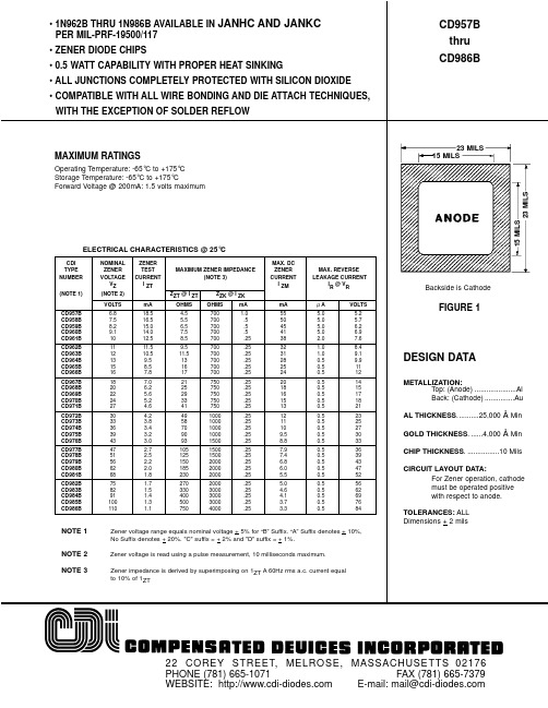
NOTE 1 NOTE 2 NOTE 3
Zener voltage range equals nominal voltage + 5% for “B” Suffix. “A” Suffix denotes + 10%, No Suffix denotes + 20%. "C" suffix = + 2% and "D" suffix = + 1%. Zener voltage is read using a pulse measurement, 10 milliseconds maximum. Zener impedance is derived by superimposing on 1ZT A 60Hz rms a.c. current equal to 10% of 1ZT
23 MILS 15 MILS
ELECTRICAL CHARACTERISTICS @ 25°C
CDI TYPE NUMBER (NOTE 1) NOMINAL ZENER VOLTAGE VZ (NOTE 2) VOLTS CD957B CD958B CD959B CD960B CD961B CD962B CD963B CD964B CD965B CD966B CD967B CD968B CD969B CD970B CD971B CD972B CD973B CD974B CD975B CD976B CD977B CD978B CD979B CD980B CD981B CD982B CD983B CD984B CD985B CD986B 6.8 7.5 8.2 9.1 10 11 12 13 15 16 18 20 22 24 27 30 33 36 39 43 47 51 56 62 68 75 82 91 100 110 mA 18.5 16.5 15.0 14.0 12.5 11.5 10.5 9.5 8.5 7.8 7.0 6.2 5.6 5.2 4.6 4.2 3.8 3.4 3.2 3.0 2.7 2.5 2.2 2.0 1.8 1.7 1.5 1.4 1.3 1.1 ZENER TEST CURRENT l ZT MAXIMUM ZENER IMPEDANCE (NOTE 3) ZZT @ l ZT OHMS 4.5 5.5 6.5 7.5 8.5 9.5 11.5 13 16 17 21 25 29 33 41 49 58 70 90 93 105 125 150 185 230 270 330 400 500 750 ZZK @ l ZK OHMS 700 700 700 700 700 700 700 700 700 700 750 750 750 750 750 1000 1000 1000 1000 1500 1500 1500 2000 2000 2000 2000 3000 3000 3000 4000 mA 1.0 .5 .5 .5 .25 .25 .25 .25 .25 .25 .25 .25 .25 .25 .25 .25 .25 .25 .25 .25 .25 .25 .25 .25 .25 .25 .25 .25 .25 .25 mA 55 50 45 41 38 32 31 28 25 24 20 18 16 15 13 12 11 10 9.5 8.8 7.9 7.4 6.8 6.0 5.5 5.0 4.6 4.1 3.7 3.3 MAX. DC ZENER CURRENT l ZM MAX. REVERSE LEAKAGE CURRENT lR @ VR
ITU-T G.957中文版

ii
ITU-T G.957 建议书 (03/2006)
目录
1 范围 .............................................................................................................................. 2 参考文献 ...................................................................................................................... 3 术语和定义 ..................................................................................................................
概述 光缆系统的参数 基于2048 kbit/s比特率的分级比特率上的数字段 非分级比特率电缆上的数字线路传输系统 FDM传输承载信道提供的数字线路系统 数字线路系统 用于用户接入ISDN的数字段和数字传输系统 海底光缆系统 本地和接入网的光线路系统 接入网 服务质量和性能-一般性和与用户相关的问题 传输媒质的特性 经传送网的数据-一般性问题 经传送网的以太网问题 接入网
ITU-T G.957建议书 与同步数字系列有关的设备和系统的光接口
摘要 本建议书规范基于同步数字系列的设备和系统的光接口的参数,以实现横向兼容性。
来源 ITU-T G.957建议书由ITU-T第15研究组(2005-2008)于2006年3月29日按照ITU-T A.8建
SMAJ5.0A中文资料

SMAJ5.0(C)A - SMAJ170(C)A 400W SURFACE MOUNT TRANSIENT VOLTAGESUPPRESSORFeaturesMaximum Ratings@ T A= 25°C unless otherwise specified·400W Peak Pulse Power Dissipation· 5.0V - 170V Standoff Voltages·Glass Passivated Die Construction·Uni- and Bi-Directional Versions Available·Excellent Clamping Capability·Fast Response Time·Plastic Material: UL FlammabilityClassification Rating 94V-0Mechanical Data·Case:SMA, Transfer Molded Epoxy·Terminals: Solderable per MIL-STD-202,Method 208·Also Available in Lead Free Plating (Matte TinFinish). Please see Ordering Information,Note 5, on Page 4·Polarity Indicator: Cathode Band(Note: Bi-directional devices have no polarityindicator.)·Marking: Date Code and Marking CodeSee Page 3·Weight:0.064 grams (approx.)·Ordering Info: See Page 3Notes: 1. Valid provided that terminals are kept at ambient temperature.2. Measured with 8.3ms single half sine-wave. Duty cycle = 4 pulses per minute maximum.3. Unidirectional units only.Notes: 4. Suffix C denotes Bi-directional device.5.V BR measured with I T current pulse = 300m s6. For Bi-Directional devices having V RWM of 10V and under, the I R is doubled.101001000100001101001000C ,J U N C T I O N C A P A C I T A N C E (p F )T V ,STANDOFF VOLTAGE (V)WM Fig.2Typical Total Capacitance255075100125150175200100755025T ,AMBIENT TEMPERATURE (°C)A Fig.1Pulse Derating CurveP E A K P U L S E D E R A T I N G I N %O F P E A K P O W E R O R C U R R E N T0123I ,P E A K P U L S E C U R R E N T (%I )P p pt,TIME (ms)Fig.4Pulse Waveform0.11.00.1101001.010100010000P ,P E A K P U L S E P O W E R (k W )d 1000.00.20.40.6255075100125150175200P M S T E A D Y S T A T E P O W E R D I S S I P A T I O N (W )(A V ),T , LEAD TEMPERATURE (°C)L Fig.6Steady State Power Derating Curve0.81.06050403020102510P E A K F O R W A R D S U R G E C U R R E N T ,(A )NUMBER OF CYCLES AT 60HzFig. 5 Maximum Non-Repetitive Surge Current20501001XX =Product type marking code (See Page 2)=Manufacturers’code marking YWW =Date code markingY =Last digit of year ex:2for 2002WW =Week code 01to52Marking InformationOrdering InformationNotes: 4.For Packaging Details, go to our website at /datasheets/ap02007.pdf.5. For Lead Free version (with Lead Free terminal finish) part number, please add "-F" suffix to part number above. Example: SMAJ170A-13-F.(Note 4)。
- 1、下载文档前请自行甄别文档内容的完整性,平台不提供额外的编辑、内容补充、找答案等附加服务。
- 2、"仅部分预览"的文档,不可在线预览部分如存在完整性等问题,可反馈申请退款(可完整预览的文档不适用该条件!)。
- 3、如文档侵犯您的权益,请联系客服反馈,我们会尽快为您处理(人工客服工作时间:9:00-18:30)。
Continental Device India Limited Data Sheet Page 1 of 3SILICON ZENER DIODES CLL957A - CLL978AOperating and Storage Junction Temperature Range Tj, Tstg -65 to +200 ºCPolarity : Cathode indicated by colour band.Note 1:CLL957 Series : Suffix A ± 10% tolerance; Suffix B ± 5% tolerance.Note 2 : Pulse test : 20ms ≤ tp ≤ 50ms.CLL957A to CLL978A, 500mW Hermetically Sealed, Glass Silicon Zener DiodesNominal Test Max Zener Impedance Max Reverse Current Type Zener Voltage Current (Note 4)MaximumNo.V Z I ZT DC Zener Current I R Maximum Test Voltage Vdc (Note 1)(Note 1, 2)(Note 2)Z ZT @ I ZT Z ZK @ I ZK I ZK I ZM µA V RVolts mA Ohms Ohms mA mA 5%10%CLL957A 6.818.5 4.5700 1.047.061.0150 5.2 4.9CLL958A 7.516.5 5.57000.542.055.075 5.7 5.4CLL959A 8.215.0 6.57000.538.050.050 6.2 5.9CLL960A 9.114.07.57000.535.045.025 6.9 6.6CLL961A 10.012.58.57000.2532.041.0107.67.2CLL962A 11.011.59.57000.2528.037.058.48.0CLL963A 12.010.511.57000.2526.034.059.18.6CLL964A 13.09.513.07000.2524.032.059.99.4CLL965A 15.08.516.07000.2521.027.0511.410.8CLL966A 16.07.817.07000.2519.037.0512.211.5CLL967A 18.07.021.07500.2517.023.0513.713.0CLL968A 20.0 6.225.07500.2515.020.0515.214.4CLL969A 22.0 5.629.07500.2514.018.0516.715.8CLL970A 24.0 5.233.07500.2513.017.0518.217.3CLL971A 27.0 4.641.07500.2511.015.0520.619.4CLL972A 30.0 4.249.010000.2510.013.0522.821.6CLL973A 33.0 3.858.010000.259.212.0525.123.8CLL974A 36.0 3.470.010000.258.511.0527.425.9CLL975A 39.0 3.280.010000.257.810.0529.728.1CLL976A 43.0 3.093.015000.257.09.6532.731.0CLL977A 47.0 2.7105.015000.25 6.48.8535.833.8CLL978A51.02.5125.015000.255.98.1538.836.7Continental Device India LimitedAn ISO/TS 16949, ISO 9001 and ISO 14001 Certified CompanyCLL957Rev 310101SOD - 80CMini MELF (LL-34)All Dimensions are in mmSOD 80C (LL-34) Mini MELF Hermetically Sealed Glass PackageDrawings are not to scaleAll Dimensions are in mmAll Dimensions are in mmIdentification Label 2,500No. of Device Notes:1.Maximum of 0.5% of the total number of components per reel may be missing-exclusively at the beginning and at the end of the reel.2.A maximum of three consecutive components may be missing, provided this gap is followed by six consecutive components.TAPE & REELDe-reeling direction De-reeling directionSOD-80C T&R 2.5K/reel 225 gm/2.5K pcs 9" x 9" x 9"40K18" x 12" x 10"19" x 19" x 20"80K 320K 7.2 kgs 28.8 kgsPACKAGENet Weight/Qty Details STANDARD PACK INNER CARTON BOXQtyOUTER CARTON BOXQty Gr Wt Size Size Packing DetailContinental Device India LimitedData SheetPage 2 of 3CLL957A - CLL978ACLL957Rev 310101Component Disposal Instructions1. CDIL Semiconductor Devices are RoHS compliant, customers are requested to please dispose as per prevailing Environmental Legislation of their Country.CLL957Rev 310101Customer NotesDisclaimerThe product information and the selection guides facilitate selection of the CDIL's Semiconductor Device(s)best suited for application in your product(s)as per your requirement.It is recommended that you completely review our Data Sheet(s)so as to confirm that the Device(s)meet functionality parameters for your application.The information furnished in the Data Sheet and on the CDIL Web Site/CD are believed to be accurate and reliable.CDIL however,does not assume responsibility for inaccuracies or incomplete information.Furthermore,CDIL does not assume liability whatsoever,arising out of the application or use of any CDIL product;neither does it convey any license under its patent rights nor rights of others.These products are not designed for use in life saving/support appliances or systems.CDIL customers selling these products (either as individual Discrete Semiconductor Devices or incorporated in their end products),in any life saving/support appliances or systems or applications do so at their own risk and CDIL will not be responsible for any damages resulting from such sale(s).CDIL strives for continuous improvement and reserves the right to change the specifications of its products without prior notice.CDIL is a registered Trademark of Continental Device India LimitedC-120 Naraina Industrial Area, New Delhi 110 028, India.Telephone + 91-11-2579 6150, 4141 1112 Fax + 91-11-2579 5290, 4141 1119email@ Continental Device India Limited Data Sheet Page 3 of 32. In Europe, please dispose as per EU Directive 2002/96/EC on Waste Electrical and Electronic Equipment (WEEE).SOD - 80CMini MELF (LL-34)元器件交易网。