RT230中文资料
BRT23H-X006中文资料

Document Number Optocoupler, Phototriac Output, Zero CrossingFeatures•High Input Sensitivity I FT = 1.0 mA •I TRMS = 300 mA•High Static dv/dt 10,000 V/µs•Electrically Insulated between Input and Output circuit•Microcomputer compatible •Trigger Current- (I FT < 1.2 mA) BRT22F , BRT23F ,- (I FT < 2 mA) BRT21H , BRT22H , BRT23H - (I FT < 3 mA) BRT21M , BRT22M , BRT23M •Available Surface Mount and on on tape and reel •Zero Voltage Crossing detector •UL File E52744 System Code "J" •Lead-free component•Component in accordance to RoHS 2002/95/EC and WEEE 2002/96/ECApplications• Industrial controls • Office equipment• Consumer appliancesDescriptionThe BRT21, BRT22, BRT23 product family consists of AC switch optocouplers with zero voltage detec-tors with two electrically insulated lateral power ICs which integrate a thyrister system, a photo detector and noise suppression at the output and an IR GaAs diode inputHigh input sensitivity is achieved by using an emitter follower phototransistor and an SCR predriver result-ing in an LED trigger current of less than 2 mA or 3 mA (DC). I nverse parallel SCRs provide commutating dv/dt greater than 10 kV/µsThe zero cross line voltage detection circuit consists of two MOSFETS and a photodiode.THe BRT21/ 22/ 23 product family isolates low-volt-age logic from 120, 230 and 380 VAC lines to control resistive, inductive or capacitive loads including motors, solenoids, high current thyristers or TRI AC and relays.Order InformationFor additional information on the available options refer to Option Information.Part RemarksBRT21H V DRM ≤ 400 V , DIP-6, 2.0 mA I FT BRT21M V DRM ≤ 400 V , DIP-6, 3.0 mA I FT BRT22F V DRM ≤ 600 V , DIP-6, 1.2 mA I FT BRT22HV DRM ≤ 600 V , DIP-6, 2.0 mA I FT BRT22M V DRM ≤ 600 V , DIP-6, 3.0 mA I FT BRT23F V DRM ≤ 800 V , DIP-6, 1.2 mA I FT BRT23H V DRM ≤ 800 V , DIP-6, 2.0 mA I FT BRT23MV DRM ≤ 800 V , DIP-6, 3.0 mA I FTBRT21H-X006V DRM ≤ 400 V, DIP-6 400 mil (option 6), 2.0 mA I FT BRT21H-X007V DRM ≤ 400 V , SMD-6 (option 7), 2.0 mA I FT BRT21M-X006V DRM ≤ 400 V, DIP-6 400 mil (option 6), 3.0 mA I FT BRT22F-X006V DRM ≤ 600 V , SMD-6 (option 7), 1.2 mA I FTBRT22F-X0067V DRM ≤ 600 V , SMD-6 (option 7), 1.2 mA I FT BRT22H-X007V DRM ≤ 600 V , SMD-6 (option 7), 2.0 mA I FT BRT22M-X006V DRM ≤ 600 V, DIP-6 400 mil (option 6), 3.0 mA I FT BRT23F-X006V DRM ≤ 800 V, DIP-6 400 mil (option 6), 1.2 mA I FT BRT23F-X007V DRM ≤ 800 V, DIP-6 400 mil (option 6), 1.2 mA I FT BRT23H-X006V DRM ≤ 800 V, DIP-6 400 mil (option 6), 2.0 mA I FT BRT23H-X007V DRM ≤ 800 V , SMD-6 (option 7), 2.0 mA I FT BRT23M-X006V DRM ≤ 800 V, DIP-6 400 mil (option 6), 3.0 mA I FT BRT23M-X007V DRM ≤ 800 V , SMD-6 (option 7), 3.0 mA I FT Document Number 83690Absolute Maximum RatingsT amb = 25°C, unless otherwise specifiedStresses in excess of the absolute Maximum Ratings can cause permanent damage to the device. Functional operation of the device is not implied at these or any other conditions in excess of those given in the operational sections of this document. Exposure to absolute Maximum Rating for extended periods of the time can adversely affect reliability.InputOutputCouplerParameterTest conditionSymbol Value Unit Reverse voltage I R = 10 µAV R 6.0V Forward current I F 60mA Surge current I FSM 2.5A Power dissipation P diss100mW Derate from 25°C1.33mW/°CParameterTest conditionPart Symbol Value Unit Peak off-state voltageI D(RMS) = 70 µABRT21V DM 400V BRT22V DM 600V BRT23V DM 800V RMS on-state current I TM300mA Single cycle surge current 3.0A Power dissipation P diss 600mW Derate from 25°C6.6mW/°CParameterTest conditionSymbol Value Unit Isolation test voltage (between emitter and detector, climate per DIN 500414, part 2, Nov. 74)t = 1.0 min.V ISO5300V RMSPollution degree (DIN VDE 0109)2Creepage ≥ 7.0mm Clearance≥ 7.0mmComparative tracking index per DIN IEC 112/VDE 0303 part 1, group IIIa per DIN VDE 6110≥ 175Isolation resistance V IO = 500 V, T amb = 25°C R IO ≥ 1012ΩV IO = 500 V, T amb = 100°CR IO ≥ 1011ΩStorage temperature range T stg - 55 to + 150°C Ambient temperature range T amb - 55 to + 100°C Soldering temperaturemax. ≤ 10 sec. dip soldering ≥ 0.5 mm from case bottom T sld260°CDocument Number Electrical CharacteristicsT amb = 25°C, unless otherwise specifiedMinimum and maximum values are testing requirements. Typical values are characteristics of the device and are the result of engineering evaluation. Typical values are for information only and are not part of the testing requirements.InputOutputParameterT est conditionSymbol MinT yp.Max Unit Forward voltage I F = 10 mA V F 1.16 1.35V Reverse current V R = 6.0 VI R 0.110µA CapacitanceV F = 0 V, f = 1.0 MHzC O 25pF Thermal resistance, junction to ambientR thja750K/WParameterT est conditionSymbol Min T yp.MaxUnit Off-state voltage I D(RMS) = 70 µAV D(RMS)424460V Repetitive peak off-state voltage I DRM = 100 µAV DRM 600V Off-state current V D = V DRM , T amb = 100°C, I F = 0 mA I D(RMS)10100µA On-state voltage I T = 300 mAV TM 1.73.0V On-state currentPF = 1.0, V T(RMS) = 1.7 VI TM 300mA Surge (non-repetitive), on-state currentf = 50 Hz I TSM 3.0A T rigger current temp. gradient∆I FT1/∆T j 7.014µA/K ∆I FT2/∆T j7.014µA/K Inhibit voltage temp. gradient ∆V DINH /∆T j-20mV/K Off-state current in inhibit state I F = I FT1, V DRMI DINH 50200µA Holding current I H 65500µA Latching current V T = 2.2 V I L 5.0mA Zero cross inhibit voltage I F = Rated I FTV IH 1525V T urn-on time V RM = V DM = V D(RMS)t on 35µs T urn-off timePF = 1.0, I T = 300 mA t off 50µs Critical rate of rise of off-state voltageV D = 0.67 V DRM , T J = 25°C dv/dt cr 10000V/µs V D = 0.67 V DRM , T J = 80°Cdv/dt cr 5000V/µs Critical rate of rise of voltage at current commutation V D = 0.67 V DRM , di/dt crq ≤ 15 A/ms, T j = 25°Cdv/dt crq 10000V/µs V D = 0.67 V DRM ,di/dt crq ≤ 15 A/ms, T j = 80°Cdv/dt crq 5000V/µs Critical rate of rise of on-state di/dt cr 8.0A/µs Thermal resistance, junction to ambientR thja125K/W Document Number 83690CouplerPower Factor ConsiderationsA snubber isn’t needed to eliminate false operation ofthe TRIAC driver because of the high static and com-mutating dv/dt with loads between 1.0 and 0.8 power factors. When inductive loads with power factors less than 0.8 are being driven, include a RC snubber or a single capacitor directly across the device to damp the peak commutating dv/ dt spike. Normally a com-mutating dv/dt causes a turning-off device to stay on due to the stored energy remaining in the turning-off device.But in the case of a zero voltage crossing optotriac,the commutating dv/dt spikes can inhibit one half of the TR AC from turning on. f the spike potential exceeds the inhibit voltage of the zero cross detection circuit, half of the TRIAC will be heldoff and not turn-on. This hold-off condition can be eliminated by using a snubber or capacitor placed directly across the optotriac as shown in Figure 1. Note that the value of the capacitor increases as a function of the load cur-rent.The hold-off condition also can be eliminated by pro-viding a higher level of LED drive current. The higher LED drive provides a larger photocurrent which causes the phototransistor to turn-on before the com-mutating spike has activated the zero cross network.Figure 2 shows the relationship of the LED drive for power factors of less than 1.0. The curve shows that if a device requires 1.5 mA for a resistive load, then 1.8 times 2.7 mA) that amount would be required to control an inductive load whose power factor is less than 0.3.ParameterTest conditionSymbol MinTyp.MaxUnit Critical rate of rise of coupled input/output voltage I T = 0 A, V RM = V DM = V D(RMS)dv IO /dt 10000V/µs Common mode coupling capacitanceC CM 0.01pF Capacitance (input-output) f = 1.0 MHz, V IO = 0 V C IO 0.8pF Isolation resistance V IO = 500 V, T amb = 25°C R is ≥ 1012ΩV IO = 500 V, T amb = 100°C R is ≥ 1011ΩTrigger currentV D = 5.0 V , F - Versions I FT 1.2mA V D = 5.0 V, H - Versions I FT 2.0mA V D = 5.0 V , M - VersionsI FT3.0mAFigure 1. Shunt Capacitance vs. Load Currentiil410_01IL -Load Current -mA(RMS)Document Number Typical Characteristics (Tamb = 25 °C unless otherwise specified)Figure 2. Normalized LED Trigger Current vs. Power Factor Figure 3. Forward Voltage vs. Forward Current Figure 4. Peak LED Current vs. Duty Factor, Tau iil410_021.21.00.80.60.40.20.0PF -Power FactorN I F t h -N o r m a l i z e d L E D T r i g g e r C u r r e n tiil410_03100101.10.70.80.91.01.11.21.31.4IF -Forward Current -mAV F -F o r w a r d V o l t a g e -Viil410_04101010101010101010100100010000t -LED Pulse Duration -sI f (p k )-P e a k L E D C u r r e n t -m AFigure 5. Maximum LED Power DissipationFigure 6. Typical Output CharacteristicsFigure 7. Current Reductioniil410_05100806040200-20-40-60050100150Ta -Ambient Temperature -°CL E D -L E D P o w e r -m Wiil410_06I T =f(V T ),parameter:T jiil410_07I TRMS =f(T A ),R thJA =150K/W Device switch soldered in pcb or base plate. Document Number 83690Figure 8. Current Reduction Figure 9. Typical Trigger Delay Time Figure 10. Typical Inhibit Current iil410_08I TRMS =f(T PIN5),R thJ–PIN5=16.5K/W Thermocouple measurement must be performed potentially separated to A1and A2.Measuring junction as near as possible at the case.Figure 11. Power Dissipation 40 to 60 Hz Line OperationFigure 12. Typical Static Inhibit Voltage LimitFigure 13. 1- Apply a Capacitor to the Supply Pins at the Load-Side40to 60Hz line operation,P tot =f(I TRMS )iil410_11iil410_12V DINHmin =f(I F /I FT 25°C),parameter:T jDevice zero voltage switch can be triggered only in hatched area below Tj curves.iil410_13Document Number Technical InformationSee Application Note for additional information.Package Dimensions in Inches (mm)Figure 14. 2 - Connect a Series Resistor to the Output and BridgeBoth by a Capacitor iil410_14V~Figure 15. 3 - Connect a Choke of Low Winding Cap. in Series,e.g., a Ringcore Choke, with Higher Load Currentsiil410_15V~ Document Number 83690Ozone Depleting Substances Policy StatementIt is the policy of Vishay Semiconductor GmbH to1.Meet all present and future national and international statutory requirements.2.Regularly and continuously improve the performance of our products, processes, distribution andoperatingsystems with respect to their impact on the health and safety of our employees and the public, as well as their impact on the environment.It is particular concern to control or eliminate releases of those substances into the atmosphere which are known as ozone depleting substances (ODSs).The Montreal Protocol (1987) and its London Amendments (1990) intend to severely restrict the use of ODSs and forbid their use within the next ten years. Various national and international initiatives are pressing for an earlier ban on these substances.Vishay Semiconductor GmbH has been able to use its policy of continuous improvements to eliminate the use of ODSs listed in the following documents.1.Annex A, B and list of transitional substances of the Montreal Protocol and the London Amendmentsrespectively2.Class I and II ozone depleting substances in the Clean Air Act Amendments of 1990 by the EnvironmentalProtection Agency (EPA) in the USA3.Council Decision 88/540/EEC and 91/690/EEC Annex A, B and C (transitional substances) respectively. Vishay Semiconductor GmbH can certify that our semiconductors are not manufactured with ozone depleting substances and do not contain such substances.We reserve the right to make changes to improve technical designand may do so without further notice.Parameters can vary in different applications. All operating parameters must be validated for each customer application by the customer. Should the buyer use Vishay Semiconductors products for any unintended or unauthorized application, the buyer shall indemnify Vishay Semiconductors against all claims, costs, damages, and expenses, arising out of, directly or indirectly, any claim of personal damage, injury or death associated with such unintended or unauthorized use.Vishay Semiconductor GmbH, P.O.B. 3535, D-74025 Heilbronn, GermanyTelephone: 49 (0)7131 67 2831, Fax number: 49 (0)7131 67 2423Document Number 。
管道中英文对照表最全的

62
内外定位环
Inner ring and outer ring
IR/OR
63
内定位环
Inner ring
IR
64
外定位环
Outer ring
OR
65
螺栓
Bolt
B
66
螺柱
Stud bolt
SB
67
螺母
Nut
NU
68
花蓝螺母
Turnbuckle
TB
69
垫圈
Washer
WSR
70
弹簧垫圈
Spring washer
79
安全阀
Safety valve
SV
80
减压阀
Pressure reducing valve
RV
81
蒸汽疏水阀
Steam trap
ST
82
泄压阀
Pressur relief valve
PRV
83
呼吸阀
Breather valve
BV
84
针形阀
Needle valve
NV
85
角阀
AV
86
隔膜阀
DV
87
Flat metallic gasket
FMG
58
齿形金属垫片
Solid metal serrated gasket
SMSG
59
透镜式金属环垫
Lens ring gasket
LER
60
八角形金属环垫
Octagonal ring gasket
OCR
61
椭圆形金属环垫
Oval ring gakset
mRoy中文说明书

mRoyIssued 01/2002/Revised 06/2007mRoy1 3 mRoy B 2 3 4. 3Bar mRoy A 1.55. 6 7 8 90 9 10 2 100 3-50 25 2mRoy1 d. e. 2. d. 3 d. 4. 5. c. 6 d. 7 a. e. a. b. NPSH c. a. a. O b. a. a. b. e. b. c. a. b. ( c. 20Hz c. )mRoy1 2 3 250 -5 2500 (Mobilgear SHC 629)13 3 3 3 3 526 6 6 6 6 7 7 7 8 9311 11 11 12413 13 13 14 145 620 2311 mRoy 2 3 4 5 6 7 8 mRoy 9 10 API 11 mRoy 12 RA020~RA120 13 RA020~RA060 14 RP001~RP070 15 RH002~RH015 16 RB070~RB330 17 RB020~RB050 18 RB020~RB330 9 RA 20 mRoy B 21 RB 22 RB 23 mRoy 24 mRoy3 4 4 6 8 9 17 23 24 25 26 32 34 36 38 40 41 43 45 46 48 49 51 5321mRoy mRoy A P HmRoy ( 1 )1 1 A(23) CmRoy 200 S.S.U.(40cps) mRoy P ( 12200cps)2 3X C H F G E D H4PTFE3F 2 G H 3 100% H 0 100%GHA G H D F E C X2A G H D F E C X3450% 50% 1 50% 0% 0 100%420 3-15psiA H P B0.7”(1.78cm) 1.5”(3.81cm)52mRoy132°C2. mRoy (100 )1°C1°C( )mRoy 9 NEMA 56C 10mRoy ( 38°C 4)(710)BBA, H, PA, H, P4 6> 5°C10°C5°CMOBILGEAR 600 XP 150 MOBILGEAR SHC 62910°CmRoy A mRoy B A mRoy0.95L 2.8L1.9L 3.8LBmRoy 50°C51 2150-20 ( 10°C)YPVC7mRoy 3/4” NPSH 1.8 NPSH NPSH mRoy 3.5Bar mRoy( )mRoy3.55Bar5 8NPSH / 1 NPSH ( ) 2. NPSHNPSH (1) NPSH)NPSH = Pa + Ph _ Pv( mRoy NPSH NPSH NPSH NPSH ( 2) NPSH) D= Dp= Lp= Le= Pa= Ph= (.435)(Sp.Gr.) Pv= 6 (PSIA) (+) (PSIA) ( _) ( ( ) ( ) ( ) ) NPSH=Pa=Ph_Pf Le( NPSH = Sp.Gr.(.0925)LpD Dp29Pf= (PSIG)( 3.2 ) NPSH= ) NPSH ) NPSH ( ( NPSH NPSH10320-40% 100% 30 1 2 3 4 30 40 mRoy 1 )5 100 PSI 7 10 20 30 15 207100% 2010 ( 100% 2 )30-40 100% 10 ( mRoy 115 1111 ( 1350 11) (50) (30) (40)95% 1 2 (mRoy A H P) (mRoy B) 3/16” 5/16” mRoy 24 481 2 431241 1 mRoy 4 O1 2 3 mRoy A, B, H, & P 1 1 1 1 4 4 1 1 mRoy A 1 4 l l 4 4 l 4 2 mRoy B 1 1 ( ) ( (H P B ) ) O 4 5 6 ( (( ) ( ( () ) ) ) )MSDS()13mRoymRoy PTFE mRoy2( ) mRoyA mRoy mRoy A mRoy() / mRoy A/ ( ( 5 ) 1 12, 14, 15, 16 & 17) SAE O142 3O mRoy P (a) ( ; (b) ):46 OmRoy A ( 1 O 2 ) ( ) ( 3 12, 14, 15, 16 & 17) 1 2133O mRoy A 1 134mRoy P5O 2 3 4 ( ) 155()6 O 7 34 5 8O O6 mRoy B 1 mRoyB 10 182 3O1 mRoy B 1 18 2 3 4 O 2 ( O ) 162 1 2 3 3 11 mRoy ) 1 2. 3. 1 6 8 10 4. 13, 16 17 3 4 5 6(A B H P &mRoy AmRoy BmRoy A7 175 2 ( 6. 7 ) ( 7) a mRoy A H P (5 ) b. c. d mRoy A 60-70 in lbs 7-8 N.m mRoy B 340-360 in lbs 38-41 N.m mRoy B 75-85in lbs 8.5-9.6 N.m 25 in mRoy mRoy B 1bs 3 N.m ( ) 5 mRoy A H 3/16” P 4” 3/16” 7/16” 4 3/16” O 265-275 in lbs 30-31 N.m 1 2 3 O E ) 1/2 ” ( 1” 2 O 1 1 41. OO O O1 2 3 4181 2 31 2 31l 33113195()20% 5 100% 524 50 70PSIG* 100% 100%()20()*( 60PSIG)( ))(21* O ) 2 3 O (2268 mRoy2392410 API2511 mRoy26RA/RP/RHRH RA&RP RA&RP 5/87/16(7/16 1 1/165/88, 9, 10 & 11)S281-0220-001 S281-0317-001 S281-0317-001 S237-0060-006 S281-0317-001 S237-0073-006 S409-0064-020 S212-0056-074 S280-0043-041 S405-0241-014 S402-0009-111 S237-0029-006 40059 S212-0055-006 S212-0054-006 S212-0053-006 S214-0025-062 S211-0030-006 S252-0125-001 252-0127-001 H61003 252-0053-001 S252-0090-201 252-0091-001 S252-0019-200 252-0026-001 H61001 252-0057-001 H61007 252-0087-001 H61005 S219-0071-006 219-0109-006 S268-0021-006 268-0018-006 S402-0095-041 S402-0095-061 S408-0109-082 S268-0037-006 S243-0058-016 S405-0039-035 S253-0015-062 S253-0024-062 S255-0019-016 1 1 1 1 1 1 1 1 1 1 1 1 2 1 1 1 1 1 1 1 1 1 1 1 1 1 1 1 1 1 1 1 1 1 1 1 3 1 1 1 1 1 110MROY P10 80MROY P1 1/1610 80 20 30 40 50 60 70 75 90 100 110RA&RP1 1/16 7/16 RA/RH/RP RA/RH/RP RA/RH/RP RA/RH/RP 1/4 NPT RA/RH/RP 9/32120125 130 140 150 160 170 180 190 200RA/RP/RH RA/RP/RH RA/RP/RH RA/RP/RH RA/RP/RH RA/RP/RH RA/RP/RH RA/RP/RH RA/RP/RH RA/RP/RH RA/RP/RH RA/RP/RH RA/RP/RH RA/RP/RH RA/RP/RH RA/RP/RH RA/RP/RH 1/2 NPT PVC 1 NPT PVC O #2-011 70DURO URETHANE RA/RP/RH PVC #6-32UNC 1/4 PVC PVC ECC CONTROL KNOB 316SS RA7/16 5/8 1-1/16 RA RA/RP RA/RP 77:1 77:1 48:1 48:1 24:1 24:1 15:1 15:1 12:1 12:1 9.5:1 9.5:1 8:118/23 SPM 18/23 SPM 29/37 SPM 29/37 SPM 59/73 SPM 59/73 SPM 94/117 SPM 94/117 SPM 117/146 SPM 112/138 SPM 148/185 SPM 148/185 SPM 176 SPM316SSPVC 304SS27RA/RP/RH210 220 230 240 250 630 RA(, 9, 10 & 11)S255-0019-062 S255-0020-016 S404-0124-096 S212-0036-039 S214-0009-006 S405-0245-011 H67510 H67511 PVC 316SS 1 1 1 1 1 2 1 1316SS GB896-86-6 RA/RP/RH RA/RP/RH RA/RP/RH #8-32UNC 1/4 RA/RP/RH 250W IEC71 B5 1440rpm 3-50-220/380V IP55/F/TEFC 250W IEC71 B5 1440rpm 3-50-220/380V IP55/F/TEFC/Ex.Proof dIIB T4 CC NEMA56C 77:1 RA/RP/RH 48:1 RA/RP/RH 24:1 RA/RP/RH/RT 15:1 RA/RP/RH 12:1 RA/RP/RH 9.5:1 RA/RP/RH 8:1 RA/RP/RH GB879-86-5 25 RA/RH/RP TIMKEN A4059 LEE LHL-625-C-1 CC NEMA 56C CC ICE71 77:1 RA/RP/RH 48:1 RA/RP/RH 24:1 RA/RP/RH/RT 15:1 RA/RP/RH 12:1 RA/RP/RH 9.5:1 RA/RP/RH 8:1 RA/RP/RH GB879-86-5 25 RA/RH/RP TIMKEN A4059 CC IEC71 B5 LEE LHL-500-C-02-MW API ICE71 77:1 RA/RP/RH 48:1 RA/RP/RH 24:1 RA/RP/RH/RT 15:1 RA/RP/RH 12:1 RA/RP/RH 9.5:1 RA/RP/RH 8:1 RA/RP/RH GB879-86-5 25 RA/RH/RP TIMKEN A4059 API IEC71 API IEC71NEMA 56C640650660 670 740IEC71,252-0157-006 S252-0126-006 H61002 S252-0090-106 S252-0019-100 H61000 H61006 H61004 S401-0005-091 S409-0064-010 403-0166-011 S252-0167-006 S252-0126-006 H61002 S252-0090-106 S252-0019-100 H61000 H61006 H61004 S401-0005-091 S409-0064-010 S60059 S252-0110-006 S252-0126-006 H61002 S252-0090-106 S252-0019-100 H61000 H61006 H61004 S401-0005-091 S409-0064-010 S409-0094-020 S219-0030-0061 1 1 1 1 1 1 1 1 1 1 1 1 1 1 1 1 1 1 1 1 1 1 1 1 1 1 1 1 1 1 1 1 1640650660 670 740IEC71, API640650660 670 680 690287107207257307407707807857907958001330134013501111111441124111444444111112111Aluminum AluminumPolycarbonate Buna N316SS 1 LiterCC NEMA 56CRA RP RH CC IEC71 B5API IEC71 B5 RAAPI NEMA 56CRA RP RH API IEC80 RA RP RHCC IEC71 B5CC IEC71 B53/8-16 5/8 (NEMA 56C )GB70-85-M8208.8 (IEC71 )LEE LHL-625-C-1CC NEMA 56C CC IEC71 B5LEE LHL-500C-02-MW1/4-20 1 (IEC71 )#8-32UNC 3/4 (API )1/214 (API IEC71) 12.7 15.8868 ( NEMA 56C API )12.7 19-78 ( API IEC80 )5/16-18NC (API IEC71)3/8-16NC 18.8 (API IEC80)5/16-18 1 1/4 (API IEC71)3/8-16 1 1/2 (API IEC80, NEMA56C)5/16 (API IEC71)3/818.8SS (API IEC80)1/4NPT RA/RP/RHO GB3452. 1-82-28 3.553/8-24 RA/RPGB mRoy A mRoy B5/32RA/RH/RP1mRoymRoy ECC272-0130-062H61010S272-0146-001H61177H61132S225-0115-099H60731S405-0029-086H60760403-0166-011S60059S405-0027-111S405-0132-031S40202H61176H61133S405-0065-013S405-0066-012S405-0017-139S405-0018-143S404-0040-028S404-0041-022S402-0009-111S30256S408-0095-071S405-2001-011H60013S405-0280-000H69002S339-0047-000339-0002-000RA/RP/RH (, 9, 10 & 11)RB19/32RB 7/8RB 1-7/16RB/RWRBRB/RWRB/RW1/4NPT19/327/81 -7/16RBRS38:138:125:125:119:119:112.5:112.5:19.5:19.5:13/4NPT RB19/327/81-1/4NPT RB1-7/16O Parker 2-113RB#6-32UNC1/4PVCRBRB#8-32UNC1/2 RBS281-0104-101S281-0104-301S281-0104-201S409-0066-020S212-0057-074S280-0046-541S256-0037-051S402-0009-111S212-0085-306S212-0085-106S212-0085-206S214-0013-162S401-0028-033H61009252-0095-001S252-0082-201252-0058-001S252-0092-201252-0093-001S252-0081-201252-0057-001S252-0088-201252-0089-001S268-0030-006S402-0095-051S402-0095-071S408-0068-032S268-0049-006S243-0059-051S405-0039-035S253-0026-062S253-0025-062S255-0020-062S404-9983-151S212-0048-039S214-0014-006S405-0245-03137/45 SPM37/45 SPM56/69 SPM56/69 SPM74/91 SPM74/91 SPM112/138 SPM112/138 SPM148/182 SPM148/182 SPM316SS 102030405060901001101201301401501601701801902002102202302402501111111111111111111111111131111111112 MROY B (8, 10 & 11)63064065066067068069070071077078078579079580013301340135011111111111111111121444111112311Polycarbonate316SS1550W IEC80B51440rpm3-50-220/380VIP55/F/TEFC750W IEC802B51450rpm3-50-220/380VIP55/F/TEFC1.1KW IEC90S B51450rpm3-50-220/380VIP55/F/TEFC550W IEC80B51440rpm3-50-220/380VIP55/F/TEFC/Ex.Proof dIIBT4750W IEC802B51450rpm3-50-220/380VIP55/F/TEFC/Ex.Proof dIIBT41.1KW IEC90S B51450rpm3-50-220/380VIP55/F/TEFC/Ex.Proof dIIBT4RB38:125:119:112.5:19.5:1GB879-86-525RBBEARING SINGLE ROW SKF#630316307GB13871-19921.189RBAPI IEC 80 B5#10-323/4IEC 80mRoy5/16-18NC3/8-161-1/45/16Z PL3/8API IEC80RBO GB3452.1-82-28 3.557/8-14RBGB mRoy A mRoy B5/32RA/RH/RPMobilgear 600 XP 1501mRoymRoy ECCAPI IEC 80H67518H67520H67530H67519H67524H67534H61113H61008S252-0082-106S252-0092-106S252-0081-106S252-0088-106S401-0005-091S409-0066-010S409-9994-000H61114S403-0121-009S6072-0388-001S405-0026-094S39238S405-0065-013S405-0018-136S404-0040-028S402-0011-031S249-0106-276S408-0095-071S405-2001-021H60013S405-0280-000H69002S339-0047-000339-0002-000MROY B ( 8, 10 & 11)12 RA020~RA120316SS316SSAlloy 20Alloy C-22PTFEPEEK316SSAlloy 20Alloy C-22A2-70A200316SSAlloy 20Alloy C-22PTFEFKMPTFE316SSAlloy 20Alloy C-22316SSAlloy 20Alloy C-22 260280285290330350358510520530540600139011111111111661112221111111 3-3/4 1.83-1/23-1/2555/16-181-1/4A2-708,O2-116 VITONOS408-0144-010S298-0061-016S298-0061-016298-0061-028298-0061-030298-0106-075298-0123-000221-0895-001S221-0858-016221-0858-029221-0858-030H65070H66304S221-0897-216221-0897-228221-0897-230S209-0020-014S408-0073-141S408-0068-065S408-0068-043S221-0896-216221-0896-228221-0896-230S280-0033-016280-0033-026280-0033-030RA020~RA120 ( 12)13 RA020~RA0602-240S RA/RP/RH316SS5TEFLONRA RP PVC5/16-18 218-8SS8-O3/89/163/32TFEPVCPVC3/8Ceramic AD995- NPTO3/89/163/32TFEPVCPVC3/8Ceramic AD995PVC-O3/89/163/32TFEPVCPVC3/8Ceramic AD995-NPTO3/89/163/32TFEPVCPVC3/8Ceramic AD995PVCS408-0144-010S298-0061-016298-0106-075221-0845-071S271-0054-015S405-0017-163H66304S408-0143-07520287S225-0032-675S20289S20290S407-0015-1112028820299S225-0032-675S20289S20290S407-0015-111S2029120292S225-0032-675S20289S20290S407-0015-1112028820302S225-0032-675S20289S20290S407-0015-111S20291407-0350-079316SSPTFEPVC18-8SSA200PTFEPTFEPVCPVCPVCPTFEPVCPVCPVCPTFEPVCPVCPVCPTFEPVCPVCPVC 260280290330340350358435490425426430440490490425426430440490495425426430440490495425426430440490500RA020~RA060 ( 13)11111662122221122221122221122221214 RP001~RP070316SS316SSAlloy 20Alloy C-22PTFEPEEK316SSAlloy 20Alloy C-22A2-70A200316SSAlloy 20Alloy C-22PTFEFKMPTFE316SSAlloy 20Alloy C-22316SSAlloy 20Alloy C-22316SSAlloy 20Alloy C-22 260280285290330350358510520530540570600139011111111111661112221111111111 3-3/4 1.83-1/23-1/2555/16-181-1/4A2-708O2-116 VITONO5/8S408-0144-010S298-0061-016S298-0061-016298-0061-028298-0061-030298-0106-075298-0123-000221-0895-001S221-0858-016221-0858-029221-0858-030H65070H66304S221-0897-216221-0897-228221-0897-230S209-0020-014S408-0073-141S408-0068-065S408-0068-043S407-0014-172407-0014-173407-0014-076221-0864-016221-0864-028221-0864-030S280-0033-016280-0033-026280-0033-030RP001~RP070 ( 14)15 RH002~RH015S401-0001-061S298-0107-006S298-0007-016298-0007-028298-0005-275221-0179-001S221-0179-016221-0179-029221-0179-030S405-0028-134S405-0028-184H66304S221-0897-216221-0897-228221-0897-230S209-0020-014S408-0073-141S408-0068-065S408-0068-043S221-0896-216221-0896-228221-0896-230S280-0033-016280-0033-026280-0033-030316SS Alloy 20PTFE 316SS Alloy 20Alloy C-22A200316SS Alloy 20Alloy C-22PTFE FKM PTFE 316SS Alloy 20Alloy C-22316SS Alloy 20Alloy C-22281282287290330350355358510520530540600139011111111162811122211111110.0621/22-1/22-1/22-7/82-7/85/16-181-1/4,RH,A2-705/16-182-1/2,RH,A2-708A200O 2-116 VITONORH002~RH015 ( 15)280285290330350355357510520530540600138013905.237/16-14 1-1/2A2-707/16-14 2-3/4A2-707/16O 3-916 1.171 0.116316SSAlloy 20PTFE316SSAlloy 20Alloy C22A2-70A2-70316SSAlloy 20Alloy C22416SSPTFEFKM316SSAlloy 20Alloy C22316SSAlloy C2211111118210111222111111 RB070~RB330 7/81-7/16 ( 16)S298-0012-006298-0016-016298-0016-028298-0013-075S221-0215-016221-0215-029221-0215-030S405-0019-149S405-0019-191S404-0042-022221-0156-016221-0156-028221-0156-030S209-0021-017S408-0073-221S408-9998-151221-0154-016221-0154-028221-0154-030S412-0023-011S280-0038-016280-0038-026S298-0014-006S298-0014-016298-0014-028298-0015-075S221-0213-016221-0213-029S405-0019-149S405-0019-171S404-0042-022S221-0897-216221-0897-228S209-0020-014S408-0073-141S408-0068-065S221-0896-216221-0896-228S412-0023-011S280-0033-016280-0033-026316SSAlloy 20PTFE316SSAlloy 20A2-70A2-70316SSAlloy 20303SSPTFEFKM316SSAlloy 20316SSAlloy C221111114481122211111 RB020~RB050 19/32 ( 17)280285290330350355357510520530540600138013903.397/16-14 1-1/2A2-707/16-14 2-1/4A2-707/16O 2-11618 RB020~RB330PVC5.23316SS316SS7/16-142-1/27/16-14 57/16430511512513514515516316SS316SS5/16-18NC5/16-18UNC10-1/43/80.7031/2NPT PVCPVC1/4 1/4O3-916 1.171 0.116 VITONS298-0012-006S211-0043-071S298-0038-071298-0013-075S221-0359-071S204-0088-016S204-0089-016S405-0019-187S405-0019-297S404-0042-022221-0464-007S204-0091-016S204-0090-016S405-0065-013S232-0014-216S407-0015-111298-0062-075S237-0049-171S243-0047-171S402-0479-028S408-9998-151221-0360-007PVCPVCPTFEPVC316SS316SSPVC316SS316SS18-8SS316SSAD995PTFEPVCPVCFKMFKMPVC 28028128529033034034535035535751051751851952152252352452652754060011111114610111421111221 RB020~RB330 7/81-7/16 ( 18)19 RA20 mRoy3-3/4 1.83-3/4 1.83-1/251/85/16-18 1-1/2A2-705/16-18 2A2-708GB5783-86 M835GB5783-86 M8205/16Z PL5/16-18NC1/8 tube1/3 PSI 3160-400psi1/41/8 NPT 3161/8NPT F1/81/8NPT1/8NPT1/81/8NPT1/81/8NPT1/8NPT 316SS#4-401/2 ZNCR#4 18-8SS#4-40nc 18.8SSNEMA 4 5-30 PSINEMA 7 5-30 PSI1/21/8NPT1/4-20 3/418-8SS1/418.8SS1/4-20nc 18.8SS1/81/80.351/8NEMA 41/8NEMA 71/80.35S408-0144-010S408-0144-010S298-0061-016S298-0061-016298-0061-028298-0061-030298-0106-075S219-0111-016221-0865-016402-0011-013S298-0091-016S298-0091-016301-0307-000S405-0017-149S405-0017-169H66304H61029H65027H65030S204-0199-006S404-0040-028S405-0065-013S40065S40066S4006740060S40062S40062S40061S40061S40063S405-0263-050S404-0095-023S405-0182-012S406-0388-001S406-0389-001S40064S405-0016-095S404-0039-022S405-0064-012407-0317-020S249-0137-116S402-0502-993S249-0136-016S249-0138-016S402-0502-993339-0036-000316SS316SSAlloy 20Alloy C-22PTFE316SS316SS316SS316SS316SSA2-70A2-70A20018-8SS316SS316SS316SS316SS316SS316SS316SS316SS316SS18-8SS18-8SS316SS18-8SS18-8SS18-8SS316SS316SS316SS316SS316SS 260280285290300310320325326350358360370380390400115011601170118011901191120012011210122012301240125012601270128012901470130011521320115212111121111116661321551111111213331112221112 inch1120 inch1 RA (19)21 RB。
HV230中文资料

Low Charge Injection 8-Channel High VoltageAnalog Switches with Bleed ResistorsFeatures❏HVCMOS ® technology for high performance ❏Very low quiescent power dissipation – 10µA ❏Output On-resistance typically 22 ohms ❏Integrated bleed resistors on the outputs ❏Low parasitic capacitances❏DC to 10MHz analog signal frequency ❏-60dB typical output off isolation at 5MHz ❏CMOS logic circuitry for low power ❏Excellent noise immunity❏On-chip shift register, latch and clear logic circuitry ❏Flexible high voltage suppliesBlock DiagramD OUTD INCLKApplications❏Medical ultrasound imaging ❏Piezoelectric transducer driversGeneral DescriptionThe Supertex HV230 and HV232 are low charge injection 8-channel high-voltage analog switch integrated circuits (ICs) with bleed resistors. These devices can be used in applications requiring high voltage switching controlled by low voltage control signals, such as ultrasound imaging and printers. The bleed resistors eliminate voltage built up on capacitive loads such as piezoelectric transducers.Input data is shifted into an 8-bit shift register which can then be retained in an 8-bit latch. To reduce any possible clock feed-through noise, Latch Enable Bar (LE) should be left high until all bits are clocked in. Using HVCMOS technology, this switch combines high voltage bilateral DMOS switches and low power CMOS logic to provide efficient control of high voltage analog signals.These ICs are suitable for various combinations of high voltage supplies, e.g., V PP /V NN : +50V/–150V, or +100V/–100V.Ordering InformationAbsolute Maximum Ratings*V DD Logic power supply voltage -0.5V to +15VV PP - V NN Supply voltage 220VV PP Positive high voltage supply -0.5V to V NN +200VV NN Negative high voltage supply +0.5V to -200V Logic input voltages -0.5V to V DD +0.3VAnalog Signal RangeV NN to V PPPeak analog signal current/channel 3.0AStorage temperature -65°C to +150°CPower dissipation:28-lead PLCC 1.2W 48-lead TQFP 1.0W 26-lead TAPP 1.0W 26-lead µ-BGA1.0W*Absolute Maximum Ratings are those values beyond which damage to the device may occur. Functional operation under these condi-tions is not implied. Continuous operation of the device at the absolute rating level may affect device reliability. All voltages are referenced to device ground.Symbol ParameterValueV DD Logic power supply voltage 1, 3 4.5V to 13.2V V PP Positive high voltage supply 1, 340V to V NN + 200V V NN Negative high voltage supply 1, 3-40V to -160V V IH High-level input voltage V DD -1.5V to V DD V IL Low-level input voltage0V to 1.5VV SIG Analog signal voltage peak to peak V NN +10V to V PP -10V 2T AOperating free air-temperature0°C to 70°CNotes:1Power up/down sequence is arbitrary except GND must be powered-up first and powered-down last.2V SIG must be V NN - V SIG - V PP or floating during power up/down transistion.3Rise and fall times of power supplies V DD , V PP , and V NN should not be less than 1.0msec.Operating Conditions *Package Options28-Lead plastic chip carrier 48-Lead TQFP 26-lead TAPP26-lead µ-BGA Die HV232PJHV232FGHV232XHV230TA--HV232GA---V PP - V NN200V 200VHV230/232 Truth TableD0D1D2D3D4D5D6D7LE CL SW0SW1SW2SW3SW4SW5SW6SW7L L L OFFH L L ONL L L OFFH L L ONL L L OFFH L L ONL L L OFFH L L ONL L L OFFH L L ONL L L OFFH L L ONL L L OFFH L L ONL L L OFFH L L ONX X X X X X X X H L HOLD PREVIOUS STATEX X X X X X X X X H OFF OFF OFF OFF OFF OFF OFF OFFNotes:1.The eight switches operate independently.2.Serial data is clocked in on the L to H transition CLK.3.The switches go to a state retaining their present condition at the rising edge of LE. When LE islow the shift register data flows through the latch.4.D OUT is high when data in shift register 7 is high.5.Shift register clocking has no effect on the switch states if LE is H.6.The clear input overrides all other inputs.DC Characteristics (over recommended operating conditions unless otherwise noted)30263848I SIG = 5mAV PP = 40V,25222732I SIG = 200mA V NN = -160VSmall Signal Switch (ON)R ONS25222730ΩI SIG = 5mA V PP = 100V,Resistance18182427I SIG = 200mA V NN = -100V 23202530I SIG = 5mAV PP = 160V,22162527I SIG = 200mA V NN = -40V Small Signal Switch (ON)∆R ONS 205.02020%I SW = 5mA, V PP = 100V,Resistance Matching V NN = -100VLarge Signal Switch (ON)R ONL 15ΩV SIG = V PP - 10V, I SIG = 1A ResistanceOutput Switch Shunt R INT 203550K ΩOutput switch to R GND Resistance I RINT = 0.5mA Switch Off Leakage I SOL5.0 1.01015µA V SIG = V PP - 10V Per SwitchDC Offset Switch Off 300100300300mV No Load DC Offset Switch On 500100500500mV No Load Pos. HV Supply Current I PPQ 1050µA ALL SWs OFF Neg. HV Supply Current I NNQ -10-50µA ALL SWs OFFPos. HV Supply Current I PPQ 1050µA ALL SWs ON, I SW = 5mA Neg. HV Supply Current I NNQ-10-50µA ALL SWs ON, I SW = 5mA Switch Output 3.03.02.0 2.0A V SIG duty cycle - 0.1%Peak CurrentOutput Switch Frequencyf SW50KHzDuty Cycle = 50%6.57.08.0V PP = 40V,V NN = -160VI PP Supply CurrentI PP4.05.0 5.5mAV PP = 100V,V NN = -100V 4.0 5.0 5.5V PP = 160V,V NN = -40V 6.57.08.0V PP = 40V,V NN = -160VI NN Supply CurrentI NN4.05.0 5.5mAV PP = 100V,V NN = -100V 4.05.0 5.5V PP = 160V,V NN = -40VLogic Supply I DD 4.0 4.0 4.0mA f CLK = 5MHz, V DD = 5.0VAverage Current Logic SupplyI DDQ 101010µA Quiescent Current Data Out Source Current I SOR 0.450.450.700.40mA V OUT = V DD - 0.7V Data Out Sink Current I SINK 0.450.450.700.40mAV OUT = 0.7VLogic Input CapacitanceC IN101010pF0°C +25°C +70°C CharacteristicsSymUnits Test Conditions min maxmintyp*max min max50KHz Output Switching Frequency with no load*Typical values only for HV232AC Characteristics (over operating conditions V DD = 5V, unless otherwise noted)0°C +25°C+70°CCharacteristicsSym min maxmin typ*maxmin maxUnits Test Condi tionsSet Up Time Before LE Rises t SD 150150150ns Time Width of LEt WLE 150150150nsClock Delay Time to Data Out t DO 551506015070150ns Time Width of CLt WCL 150150150ns Set Up Time Data to Clock t SU 15158.020ns Hold Time Data from Clock t h 353535nsClock Freqf CLK 5.0 5.0 5.0MHz 50% duty cycle f DATA = f CLK /2Clock Rise and Fall Times t r , t f 1.0 1.0 1.0µs Turn On Time t ON 5.0 5.0 5.0µs V SIG = V PP -10V,R L = 10K ΩTurn Off Timet OFF5.0 5.0 5.0µsV SIG = V PP -10V,R L = 10K Ω202020V PP = 160V,V NN = -40VMaximum V SIG Slew Ratedv/dt202020V/nsV PP = 100V,V NN = -100V 202020V PP = 40V,V NN = -160VOff IsolationKO-30-30-33-30dB f = 5MHz,1K Ω//15pF load -58-58-58dB f = 5MHz,50Ω load Switch Crosstalk K CR -60-60-70-60dBf = 5MHz,50Ω load Output Switch Isolation I ID 300300300mA 300ns pulse width,Diode Current2.0% duty cycle Off Capacitance SW to GND C SG(OFF) 5.017 5.01217 5.017pF 0V, 1MHz On Capacitance SW to GNDC SG(ON)25502538502550pF0V, 1MHzAC Characteristics (over operating conditions V DD = 5V, unless otherwise noted)V PP = 40V, V NN = -160V, R L = 50ΩV PP = 100V, V NN = -100V, R L = 50ΩV PP = 160V, V NN = -40V, R L = 50Ω150150150150150150mVOutput Voltage Spike+25°C UnitsCharacteristics Sym Test Conditionsmin typ* max+V SPK-V SPK +V SPK -V SPK +V SPK -V SPK*Typical values only for HV232Electrical Characteristics*Typical values only for HV232HV230/232Test CircuitsSwitch OFF LeakageV PP–10VDC Offset ON/OFFV OUTT ON /T OFF T est CircuitV Isolation Diode Current V SIGCrosstalkK CR = 20LogOUT V INV IN Charge Injection V SIGV Q = 1000pF x ∆V OUTOutput Voltage SpikeOFF Isolation O OUT V INVHV230/232LE CLV PPV NN V DDRGNDD OUTD INCLKLogic Timing WaveformsD N - 1NN + 1D D OUT(TYP)CLRHV230/232Package OutlinesHV232 28-Pin J-Lead Pin Function PinFunction 1SW315N/C 2SW316D IN 3SW217CLK 4SW218LE 5SW119CL 6SW120D OUT 7SW021SW78SW022SW79N/C 23SW610V PP 24SW611R GND 25SW512V NN 26SW513GND 27SW414V DD28SW4HV232 48-Pin TQFP Pin Function 1SW52N/C 3SW44N/C 5SW46N/C 7N/C 8SW39N/C 10SW311N/C 12SW213N/C 14SW215N/C 16SW117N/C 18SW119N/C 20SW021N/C 22SW023N/C 24V PPPinFunction 25V NN 26N/C 27R GND 28GND 29V DD 30N/C 31N/C 32N/C 33D IN 34CLK 35LE 36CLR 37D OUT 38N/C 39SW740N/C 41SW742N/C 43SW644N/C 45SW646N/C 47SW548N/CPin ConfigurationsTop View28-Pin J-Lead Package123412131415161718262728Top View 48-Pin TQFPPin 1Pin 12HV230/232HV232GA Package Outline (µ-BGA)INDEXNotes:1.Dimensioning and tolerance per ASME Y14.5M-1994.2.Do not subject part to ultrasonic cleaning or intense UV.3.Contact ball position per JESD 95-1, SPP-010.4.Units are in millimeters.HV230/232µ-BGA Function TableBall Location FunctionA4SW1C3SW2C4SW1C5SW0C6V PPC7V NND1SW3D3SW3D4SW2D5SW0D6R GNDD7GNDD9V DDE1SW4E3SW4E4SW5E5SW7E6LEE7CLKE9D INF3SW5F4SW6F5SW7F6D OUTF7CLRH4SW6HV230/232123456789101112131415161718Pad connections are on the backside of the packageBottom ViewDimensions are in mmPin ConfigurationPackage DimensionsPad Diagram#n i P n o i t c n u F #n i P n o i t c n u F 14W S 41V D D 23W S 51D N I 33W S 61K L C 42W S 71r a b E L 52W S 81R L C 61W S 91D T U O 71W S 027W S 80W S 127W S 90W S 226W S 01V P P 326W S 11V N N 425W S 21R D N G 525W S 31DN G 624W S 元器件交易网。
nts-230系列网络电力仪表技术说明书v1.00

(版权所有,翻版必究)
NTS-230 系列网络电力仪表
技 术 说 明 书
版 本:V1.05 2008 பைடு நூலகம் 06 月
在试图安装、操作或维护此设备之前,请仔细阅读本说明,拿到它 并逐步熟悉这种仪表。以下特殊信息可能贯穿出现在本手册中或在设备 上,用来警示潜在的危险或对于阐释和规定操作规程的信息提请注意。
I
NTS-230 系列网络电力仪表技术说明书
3.6.6 最值统计-----------------------------------------------------------------67 3.6.7 实时时钟-----------------------------------------------------------------68 3.6.8 输入输出:--------------------------------------------------------------68 3.6.9 越限告警-----------------------------------------------------------------72 3.6.10 系统事件告警 ---------------------------------------------------------75
4.3 通讯地址表 --------------------------------------------------------------------84 4.3.1 数据地址分布表--------------------------------------------------------84 4.3.2 实时测量值地址表-----------------------------------------------------85 4.3.3 系统参数设置地址表 --------------------------------------------------88 4.3.4 电度量地址表 -----------------------------------------------------------92 4.3.5 开关量地址表 -----------------------------------------------------------97 4.3.6 系统事件记录地址表 --------------------------------------------------98 4.3.7 越限事件记录地址表 ------------------------------------------------ 101 4.3.8 最值记录地址表 ------------------------------------------------------ 102 4.3.9 系统时钟地址表 ------------------------------------------------------ 106 4.3.10 控制命令地址表 ---------------------------------------------------- 106 4.3.11 固件版本信息地址表(内部使用,用户手册不能出现)-- 107
RT334012中文资料

10A/10A @ 30VDC
12A/12A @ 250VAC
12A/12A @ 30VDC
3/4 HP @ 480VAC*
1/2 HP @ 240VAC*
1/3 HP @ 120VAC*
48 LRA/10 FLA @ 240VAC*
TV-3 @ 120VAC*
A300, 720VA @ 240VAC*
元器件交易网
Ordering Information
Typical Part Number B RT
1
3
1. Basic Series: RT = Miniature, printed circuit board relay.
2. Enclosure: 1 = 1 pole 12A, Pinning 3.5mm, flux-tight (Code 1). 3 = 1 pole 16A, Pinning 5mm, flux-tight (Code 3). 4 = 2 pole 8A, Pinning 5mm, flux-tight (Code 5).
.50 (12.7)
6X .031 X .020 (.80 X .52)
2X .020 X .020 (.52 X .52)
.17 (4.3)
PC Board Layouts (Bottom View)
1 Pole 12A 3.5mm
.051 DIA. (1.30)
1 Pole 16A 2 Pole 8A 5mm
Resistive Resistive
Motor Motor Motor Motor Tungsten Pilot Duty Pilot Duty
Resistive/GP Resistive
SI2302-TP;中文规格书,Datasheet资料

Revision: A
/
3 of 5
2011/01/01
VGS, Gate to Source Voltage (V) ID, Drain Current (A)
VTH, Normalized Gate-Source Threshold Voltage
RDS(ON), Normalized RDS(ON), On-Resistance(Ohms)
IS, Source-drain current (A)
ID, Drain Current (A)
SI2302
10 25 C
Maximum Ratings @ 25OC Unless Otherwise Specified
Symbol VDS ID IDM VGS
PD R©JA
TJ
TSTG
Parameter Drain-source Voltage Drain Current-Continuous Drain Current-Pulsed a Gate-source Voltage
MCC
TM
Micro Commercial Components
5 VDS=10V ID=3.6A
4
3
2
1
0
0
2
4
6
Qg, Total Gate Charge (nC)
Figure 7. Gate Charge
VDD
RL VIN
D
VOUT
VGS
RGEN G
S
Figure 9. Switching Test Circuit
相机术语中英文对照表
86 87 88 89 90 91 92 93 94 95 96 97 98 99 100 101 102 103 104 105 106 107
108 109 110 111 112 113 114 115 116 117 118 119 120 121 122 123 124 125 126 127 128
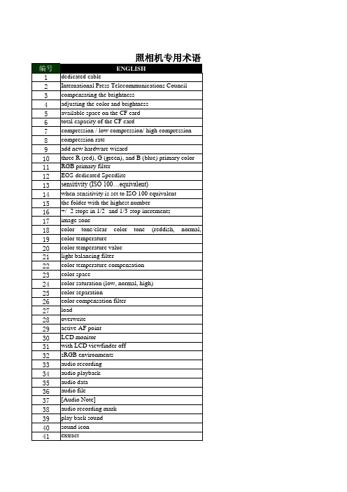
照相机专用术语
编号 1 2 3 4 5 6 7 8 9 10 11 12 13 14 15 16 17 18 19 20 21 22 23 24 25 26 27 28 29 30 31 32 33 34 35 36 37 38 39 40 41
ENGLISH dedicated cable International Press Telecommunications Council compensating the brightness adjusting the color and brightness available space on the CF card total capacity of the CF card compression / low compression/ high compression compression rate add new hardware wizard three R (red), G (green), and B (blue) primary color RGB primary filter EOS-dedicated Speedlite sensitivity (ISO 100…equivalent) when sensitivity is set to ISO 100 equivalent the folder with the highest number +/- 2 stops in 1/2- and 1/3-stop increments image zone color tone/clear color tone (reddish, normal, yellowish) color temperature color temperature value light balancing filter color temperature compensation color space color saturation (low, normal, high) color separation color compensation filter load overwrite active AF point LCD monitor with LCD viewfinder off sRGB environments audio recording audio playback audio data audio file [Audio Note] audio recording mark play back sound sound icon extract
- 1、下载文档前请自行甄别文档内容的完整性,平台不提供额外的编辑、内容补充、找答案等附加服务。
- 2、"仅部分预览"的文档,不可在线预览部分如存在完整性等问题,可反馈申请退款(可完整预览的文档不适用该条件!)。
- 3、如文档侵犯您的权益,请联系客服反馈,我们会尽快为您处理(人工客服工作时间:9:00-18:30)。
Document Number: 50029 Revision 22-Jun-05
21
DIAL CG115 ()
4 holes Ø 3.5 4 3 2 1 0 50 98 115 10 9 5 2 holes Ø 6
Ø 12
6 7 8 98 115
Ø 76 Ø 10 16
MARKING
SFERNICE trademark, series, style, ohmic value (in Ω or kΩ), tolerance (in %), maximum current in A, manufacturing date
ELECTRICAL SPECIFICATIONS
Ohmic Range Tolerance Standard Power Rating Variation Law Limiting Element Voltage Dielectric Strength Insulation Resistance 1Ω to 22kΩ ± 10% 250 W at 25°C linear sectorial winding 1500V 2000VRMS 103MΩ(500Vcc)
thumb wheel nut min. panel cut-out Ø 32
18 panel
17
SPINDLES
Ø mm 10 DISTANCE TO MOUNTING PLATE MM 50 SCREW DRIVER SLOT WITHOUT CODE AS
For any special requirement on request : spindle flats, etc. Please supply detailed drawing. COMMAND KNOB 60JF (OPTION)
元器件交易网
RT230
Vishay Sfernice
Wirewound Rheostat/Potentiometer
FEATURES
• 250 Watt at 25°C • CCTU 05-03B (PA7) • Vitreous style
DIMENSIONS in millimeters
OHMIC TOLERANCE VALUE
Optional
ACC OPTIONS MODEL
60JF KNOB
CG115 DIAL
for special spindles please supply detailed drawing
90
For technical questions, contact sfer@
RT230-PA7
PANEL CUT OUT DETAILS
143 + 3,5
60
15
50
-0 10 - 0, 05
83 Screw M5
Ø 12
60 75 Mounting side 50 + 2 AS
2 holes Ø 5.5
MECHANICAL SPECIFICATIONS
Mechanical Protection Mechanical Travel Operating Torque End Stop Torque Unit Weight Vitreous 300° ± 5° 1 to 50 Ncm 200 Ncm 1300 g
ORDERING PROCEDURE
VITREOUS RT SERIES 230 STYLE SPINDLE LOCKING DEVICE Optional L VARIATION LAW SPECIAL DESIGN Method N° Optional XXX OTHER SPECIAL REQUIREMENTS WINDING AS SPINDLE (Code) 10kΩ ± 10%
For technical questions, contact sfer@
89
元器件交易网
RT230
Vishay Sfernice
LOCKING DEVICE
This is supplied as an option. The available spindle length is according to the panel thick-ness. Order reference : DBA10.
Standard On request
ENVIRONMENTAL SPECIFICATIONS
Temperature Range Climatic Category – 55°C + 320°C CCTU 454 CEI 55/200/56
Document Number: 50029 Revision 22-Jun-05
Wirewound Rheostat/Potentiometer
PARTICULAR CHARACTERISTICS
NOMINAL RESISTANCE Ω 1 1.5 2.2 3.3 4.7 6.8 10 15 22 33 47 68 100 150 220 330 470 680 1k 1.5k 2.2k 3.3k 4.7k 6.8k 10k 15k 22k MAX. SERVICE VOLTAGE V 15.2 18.6 22.5 27.6 32.9 31.5 48 58.7 71.1 87.1 104 125 152 186 225 276 329 395 480 587 711 871 1040 1250 1500 1940 2000 MAX. CURRENT THROUGH WIPER A 15.2 12.4 10.2 8.36 7 5.82 4.80 3.92 3.23 2.64 2.21 1.84 1.52 1.24 1.02 0.836 0.700 0.582 0.480 0.392 0.323 0.264 0.221 0.184 0.150 0.13 0.091