883-Utilization of degossypolled
脱酚棉籽蛋白在水产饲料中的应用

Xue Min Luo Lin
薛敏
罗琳
Beijing Aquaculture Nutrition Research Centre, Beijing
北京友谊通元水产技术开发中心
Why research on degossypolled cottonseed protein (DCP)
研究脱酚棉籽蛋白在水产饲料中的应用的目的
Fish meal is deficient and expensive resources,phosphorus excretion •鱼粉是很好的水产饲料蛋白源,但资源短缺,价格昂贵,磷污 染严重 The market price of the fish has been decreased rapidly •由于养殖规模的扩大和产量的大幅提高,水产品价格降幅较大 The importance of vegetable alternative proteins •植物性替代蛋白源成为研究热点
utilizationofdegossypolledcottonseedproteininaquaticfeed脱酚棉籽蛋白在水产饲料中的应用脱酚棉籽蛋白在水产饲料中的应用xueminluolin薛敏薛敏罗琳罗琳beijingaquaculturenutritionresearchcentrebeijing北京友谊通元水产技术开发中心北京友谊通元水产技术开发中心whyresearchondegossypolledcottonseedproteindcp研究脱酚棉籽蛋白在水产饲料中的应用的目的研究脱酚棉籽蛋白在水产饲料中的应用的目的fishmealisdeficientandexpensiveresourcesphosphorusexcretion?鱼粉是很好的水产饲料蛋白源但资源短缺价格昂贵磷污鱼粉是很好的水产饲料蛋白源但资源短缺价格昂贵磷污染严重染严重themarketpriceofthefishhasbeendecreasedrapidly?由于养殖规模的扩大和产量的大幅提高水产品价格降幅较大由于养殖规模的扩大和产量的大幅提高水产品价格降幅较大theimportanceofvegetablealternativeproteins?植物性替代蛋白源成为研究热点植物性替代蛋白源成为研究热点continue研究脱酚棉籽蛋白在水产饲料中的应用的目的研究脱酚棉籽蛋白在水产饲料中的应用的目的theannualproductofcottonseedisabout5milliontoninchinabutnormaluseofcottonseedmealinfeedislessthan15becauseofitslowlysinemethioninecystineavailabilityandtoxicityofgossypol
Leuze electronic BCL 308i OM 100 D H Stationary ba

BCL 308i OM 100 D HStationary bar code readerFigure can varyTechnical dataBasic dataSeries BCL 300iSpecial designSpecial design HeatingFunctionsFunctions Alignment modeLED indicatorHeatingAutoControlAutoReflActCode fragment technologyAutoConfigReference code comparisonCharacteristic parametersMTTF110 yearsRead dataCode types, readable GS1 Databar OmnidirectionalCode 93Code 39GS1 Databar ExpandedEAN 8/13GS1 Databar LimitedUPC2/5 InterleavedCode 128CodabarScanning rate, typical1,000 scans/sBar codes per reading gate, max. number64 Piece(s)Optical dataReading distance40 ... 300 mmLight source Laser,RedLaser light wavelength655 nmLaser class2,IEC/EN 60825-1:2007Transmitted-signal shape ContinuousModule size0.2 ... 0.5 mmReading method Oscillating-mirror scannerBeam deflection Via rotating polygon wheel + stepping motor with mirror Light beam exit Zero position at side at angle less than 90°Oscillating mirror frequency10 HzMax. swivel angle15 °Electrical dataProtective circuit Polarity reversal protectionPerformance dataSupply voltage18 ... 30 V,DCPower consumption, max.45 WInputs/outputs selectableCurrent, max.60 mANumber of inputs/outputs selectable 2 Piece(s)Input current, max.8 mAInterfaceType EthernetEthernetArchitecture ServerClientAddress assignment DHCPManual address assignment Transmission speed100 Mbit/s10 Mbit/sFunction ProcessSwitch functionality IntegratedTransmission protocol TCP/IP , UDPService interfaceType USBUSBFunction ServiceConfiguration via softwareConnectionNumber of connections 1 Piece(s)Connection 1Type of connection Plug connectorFunction Service interfaceConnection to deviceData interfaceBUS INPWR / SW IN/OUTNo. of pins32 -pinType MaleMechanical dataDesign CubicDimension (W x H x L)125 mm x58 mm x110 mmHousing material Metal,Diecast aluminumLens cover material GlassNet weight580 gHousing color BlackRedType of fastening Via optional mounting deviceFastening on backDovetail groovesOperation and displayType of display LEDMonochromatic graphic display, 128 x 32 pixels Number of LEDs 2 Piece(s)Type of configuration Via web browserEnvironmental dataAmbient temperature, operation-35 ... 40 °CAmbient temperature, storage-20 ... 70 °CRelative humidity (non-condensing)0 ... 90 %CertificationsDegree of protection IP 65Protection class IIICertifications c UL USTest procedure for EMC in accordance with standard EN 55022EN 61000-4-2, 3, -4, -6 Test procedure for shock in accordance with standard IEC 60068-2-27, test Ea Test procedure for continuous shock in accordance with standard IEC 60068-2-29, test Eb Test procedure for vibration in accordance with standard IEC 60068-2-6, test FcClassification*********27280102*********27280102ETIM 5.0EC002550Dimensioned drawingsAll dimensions in millimetersElectrical connectionConnection 1Type of connection Plug connector Function Service interfaceConnection to deviceData interfaceBUS INPWR / SW IN/OUTNo. of pins32 -pinConnection 1Type MaleDiagramsReading field curvex Reading field distance [mm]y Reading field width [mm]Lateral reading field curveOperation and displayLEDsLED Display Meaning1PWR Green, flashing Device ok, initialization phase Green, continuous light Device OKGreen, briefly off - on Reading successfulgreen, briefly off - briefly red - on Reading not successfulOrange, continuous light Service modeRed, flashing Device OK, warning setRed, continuous light Error, device error2BUS Green, flashing InitializationGreen, continuous light Bus operation okRed, flashing Communication errorRed, continuous light Bus errorAccessoriesConnection technology - Connection cablesPart no.Designation Article Description50132077KD U-M12-5A-V1-020Connection cable Connection 1: Connector, M12, Axial, Female, A-coded, 5 -pin Connection 2: Open endShielded: NoCable length: 2,000 mmSheathing material: PVC50132079KD U-M12-5A-V1-050Connection cable Connection 1: Connector, M12, Axial, Female, A-coded, 5 -pin Connection 2: Open endShielded: NoCable length: 5,000 mmSheathing material: PVC50132080KD U-M12-5A-V1-100Connection cable Connection 1: Connector, M12, Axial, Female, A-coded, 5 -pin Connection 2: Open endShielded: NoCable length: 10,000 mmSheathing material: PVC50132432KD U-M12-5A-V1-300Connection cable Connection 1: Connector, M12, Axial, Female, A-coded, 5 -pin Connection 2: Open endShielded: NoCable length: 30,000 mmSheathing material: PVC50135073KS ET-M12-4A-P7-020Connection cable Suitable for interface: EthernetConnection 1: Connector, M12, Axial, Male, D-coded, 4 -pinConnection 2: Open endShielded: YesCable length: 2,000 mmSheathing material: PUR50135074KS ET-M12-4A-P7-050Connection cable Suitable for interface: EthernetConnection 1: Connector, M12, Axial, Male, D-coded, 4 -pinConnection 2: Open endShielded: YesCable length: 5,000 mmSheathing material: PUR50135075KS ET-M12-4A-P7-100Connection cable Suitable for interface: EthernetConnection 1: Connector, M12, Axial, Male, D-coded, 4 -pinConnection 2: Open endShielded: YesCable length: 10,000 mmSheathing material: PUR50135076KS ET-M12-4A-P7-150Connection cable Suitable for interface: EthernetConnection 1: Connector, M12, Axial, Male, D-coded, 4 -pinConnection 2: Open endShielded: YesCable length: 15,000 mmSheathing material: PUR50135077KS ET-M12-4A-P7-300Connection cable Suitable for interface: EthernetConnection 1: Connector, M12, Axial, Male, D-coded, 4 -pinConnection 2: Open endShielded: YesCable length: 30,000 mmSheathing material: PURConnection technology - Interconnection cablesPart no.Designation Article Description50106901KBET-10000-SSA InterconnectioncableSuitable for interface: EthernetConnection 1: Connector, M12, Axial, Male, D-coded, 4 -pinConnection 2: Connector, M12, Axial, Male, D-coded, 4 -pinShielded: YesCable length: 10,000 mmSheathing material: PUR50106902KBET-15000-SSA InterconnectioncableSuitable for interface: EthernetConnection 1: Connector, M12, Axial, Male, D-coded, 4 -pinConnection 2: Connector, M12, Axial, Male, D-coded, 4 -pinShielded: YesCable length: 15,000 mmSheathing material: PUR50106899KB ET-2000-SSA Interconnectioncable Suitable for interface: EthernetConnection 1: Connector, M12, Axial, Male, D-coded, 4 -pin Connection 2: Connector, M12, Axial, Male, D-coded, 4 -pin Shielded: YesCable length: 2,000 mmSheathing material: PUR50106905KBET-30000-SSA InterconnectioncableSuitable for interface: EthernetConnection 1: Connector, M12, Axial, Male, D-coded, 4 -pinConnection 2: Connector, M12, Axial, Male, D-coded, 4 -pinShielded: YesCable length: 30,000 mmSheathing material: PUR50106900KB ET-5000-SSA Interconnectioncable Suitable for interface: EthernetConnection 1: Connector, M12, Axial, Male, D-coded, 4 -pin Connection 2: Connector, M12, Axial, Male, D-coded, 4 -pin Shielded: YesCable length: 5,000 mmSheathing material: PUR50117011KB USB A - USBminiB Service line Suitable for interface: USBConnection 1: USBConnection 2: USBShielded: YesCable length: 1,500 mmSheathing material: PVC50135080KSS ET-M12-4A-RJ45-A-P7-020InterconnectioncableSuitable for interface: EthernetConnection 1: Connector, M12, Axial, Male, D-coded, 4 -pinConnection 2: RJ45Shielded: YesCable length: 2,000 mmSheathing material: PUR50135081KSS ET-M12-4A-RJ45-A-P7-050InterconnectioncableSuitable for interface: EthernetConnection 1: Connector, M12, Axial, Male, D-coded, 4 -pinConnection 2: RJ45Shielded: YesCable length: 5,000 mmSheathing material: PUR50135082KSS ET-M12-4A-RJ45-A-P7-100InterconnectioncableSuitable for interface: EthernetConnection 1: Connector, M12, Axial, Male, D-coded, 4 -pinConnection 2: RJ45Shielded: YesCable length: 10,000 mmSheathing material: PURPart no.Designation Article Description50135083KSS ET-M12-4A-RJ45-A-P7-150InterconnectioncableSuitable for interface: EthernetConnection 1: Connector, M12, Axial, Male, D-coded, 4 -pinConnection 2: RJ45Shielded: YesCable length: 15,000 mmSheathing material: PUR50135084KSS ET-M12-4A-RJ45-A-P7-300InterconnectioncableSuitable for interface: EthernetConnection 1: Connector, M12, Axial, Male, D-coded, 4 -pinConnection 2: RJ45Shielded: YesCable length: 30,000 mmSheathing material: PURConnection technology - ConnectorsPart no.Designation Article Description50108991D-ET1Connector Suitable for interface: EthernetConnection: RJ4550020501KD 095-5A Connector Connection: Connector, M12, Axial, Female, A-coded, 5 -pin50112155S-M12A-ET Connector Suitable for interface: EthernetConnection: Connector, M12, Axial, Male, D-coded, 4 -pinConnection technology - Terminal boxesPart no.Designation Article Description50131255*ME 308 103Connection unit Suitable for: BCL 308iSuitable for interface: EthernetNumber of connections: 4 Piece(s)Connection: Cable with connector, M12, 900 mm 50131254*ME 308 104Connection unit Suitable for: BCL 308iSuitable for interface: EthernetNumber of connections: 5 Piece(s)Connection: Cable with connector, M12, 900 mm 50116466*MK 308Connection unit Suitable for: BCL 308iSuitable for interface: EthernetNumber of connections: 4 Piece(s)Connection: Terminal50114823*MS 308Connection unit Suitable for: BCL 308iSuitable for interface: EthernetNumber of connections: 4 Piece(s)Connection: Connector, M12* Necessary accessories, please order separatelyConnection technology - AdaptersPart no.Designation Article Description50109832KDS ET-M12 /RJ45 W-4P Adapter Suitable for: EthernetNumber of connections: 2 Piece(s)Connection 1: Connector, M12, Angled, Female, D-coded, 4 -pinConnection 2: RJ45Mounting technology - Mounting bracketsPart no.Designation Article Description50121433BT 300 W Mounting device Contains: 4x M4 x 10 screw, 4x position washers, 4x lockwashersDesign of mounting device: Angle, L-shapeMounting bracket, at system: Through-hole mountingMounting bracket, at device: Screw typeType of mounting device: AdjustableMaterial: MetalMounting technology - Rod mountsPart no.Designation Article Description50121434BT 300 - 1Mounting device Contains: 4x M4 x 10 screw, 4x position washers, 4x lockwashersDesign of mounting device: Mounting systemMounting bracket, at system: For 12 mm rod, For 14 mm rod,For 16 mm rodMounting bracket, at device: Screw typeType of mounting device: Turning, 360°, AdjustableMaterial: Metal50027375BT 56Mounting device Design of mounting device: Mounting systemMounting bracket, at system: For 16 mm rod, For 18 mm rod,For 20 mm rodMounting bracket, at device: ClampableMaterial: MetalTightening torque of the clamping jaws: 8 N·mFunctions: Static applications50121435BT 56 - 1Mounting device Design of mounting device: Mounting systemMounting bracket, at system: For 12 mm rod, For 14 mm rod,For 16 mm rodMounting bracket, at device: ClampableMaterial: MetalTightening torque of the clamping jaws: 8 N·mFunctions: Static applicationsMounting technology - OtherPart no.Designation Article Description50111224BT 59Mounting bracket Mounting bracket, at system: Groove mountingMounting bracket, at device: ClampableMaterial: Metal50124941BTU 0300M-W Mounting device Mounting bracket, at system: Through-hole mountingMounting bracket, at device: Clampable, Groove mountingMaterial: MetalReflective tapes for standard applicationsPart no.Designation Article Description50106119REF 4-A-100x100Reflective tape Design: RectangularReflective surface: 100 mm x 100 mmMaterial: PlasticChemical designation of the material: PMMAFastening: Self-adhesiveNotesObserve intended use!•This product is not a safety sensor and is not intended as personnel protection.•The product may only be put into operation by competent persons.•Only use the product in accordance with its intended use.WARNING! LASER RADIATION – LASER CLASS 2Never look directly into the beam!The device satisfies the requirements of IEC60825-1:2007 (EN60825-1:2007) safety regulations for a product of laser class2as well as the U.S.21CFR1040.10 regulations with deviations corresponding to "Laser Notice No.50" from June 24, 2007.•Never look directly into the laser beam or in the direction of reflected laser beams! If you look into the beam path over a longer time period, there is a risk of injury to the retina.•Do not point the laser beam of the device at persons!•Interrupt the laser beam using a non-transparent, non-reflective object if the laser beam is accidentally directed towards a person.•When mounting and aligning the device, avoid reflections of the laser beam off reflective surfaces!•CAUTION! Use of controls or adjustments or performance of procedures other than specified herein may result in hazardous light exposure.•Observe the applicable statutory and local laser protection regulations.•The device must not be tampered with and must not be changed in any way.There are no user-serviceable parts inside the device.Repairs must only be performed by Leuze electronic GmbH + Co. KG.NOTEAffix laser information and warning signs!Laser information and warning signs are affixed to the device. In addition, self-adhesive laser information and warning signs (stick-on labels) are supplied in several languages.•Affix the laser information sheet to the device in the language appropriate for the place of use. When using the device in the US, use the stick-on label with the "Complies with 21CFR1040.10" note.•Affix the laser information and warning signs near the device if no signs are attached to the device (e.g. because the device is too small) or if the attached laser information and warning signs are concealed due to the installation position.•Affix the laser information and warning signs so that they are legible without exposing the reader to the laser radiation of the device or other optical radiation.。
MIL-STD-883G temperature-cycling test
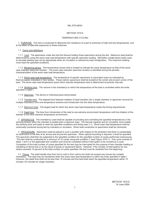
MIL-STD-883GMETHOD 1010.8TEMPERATURE CYCLING1. PURPOSE. This test is conducted to determine the resistance of a part to extremes of high and low temperatures, and to the effect of alternate exposures to these extremes.1.1 Terms and definitions.1.1.1 Load. The specimens under test and the fixtures holding those specimens during the test. Maximum load shall be determined by using the worst case load temperature with specific specimen loading. Monolithic (single block) loads used to simulate loading may not be appropriate when air circulation is reduced by load configuration. The maximum loading must meet the specified conditions.1.1.2 Monitoring sensor. The temperature sensor that is located to indicate the same temperature as that of the worst case indicator specimen location. The worst case indicator specimen location is identified during the periodic characterization of the worst case load temperature.1.1.3 Worst case load temperature. The temperature of specific specimens or equivalent mass as indicated by thermocouples imbedded in their bodies. These indictor specimens shall be located at the center and at each corner of the load. The worst case load temperature (point which reaches temperature last) is determined at periodic intervals.1.1.4 Working zone. The volume in the chamber(s) in which the temperature of the load is controlled within the limits specified in table I.1.1.5 Specimen. The device or individual piece being tested.1.1.6 Transfer time. The elapsed time between initiation of load transition (for a single chamber or specimen removal for multiple chambers) from one temperature extreme and introduction into the other temperature.1.1.7 Maximum load. The largest load for which the worst case load temperature meets the timing requirements.1.1.8 Dwell time. The time from introduction of the load to one extreme environment temperature until the initiation of the transfer to the other extreme temperature environment.2. APPARATUS. The chamber(s) used shall be capable of providing and controlling the specified temperatures in the working zone(s) when the chamber is loaded with a maximum load. The thermal capacity and air circulation must enable the working zone and loads to meet the specified conditions and timing (see3.1). Worst case load temperature shall be continually monitored during test by indicators or recorders. Direct heat conduction to specimens shall be minimized.3. PROCEDURE. Specimens shall be placed in such a position with respect to the airstream that there is substantially no obstruction to the flow of air across and around the specimen. When special mounting is required, it shall be specified. The specimen shall then be subjected to the specified condition for the specified number of cycles performed continuously. This test shall be conducted for a minimum of 10 cycles using test condition C (see Figure 1010-1). One cycle consists of steps 1 and 2 or the applicable test condition and must be completed without interruption to be counted as a cycle. Completion of the total number of cycles specified for the test may be interrupted for the purpose of test chamber loading or unloading of device lots or as the result of power or equipment failure. However, if the number of interruptions for any reason exceeds 10 percent of the total number of cycles specified, the test must be restarted from the beginning.3.1 Timing. The total transfer time from hot to cold or from cold to hot shall not exceed one minute (for multiple chambers). The load may be transferred when the worst case load temperature is within the limits specified in table I. However, the dwell time shall not be less than 10 minutes and the load shall reach the specified temperature within 15 minutes (16 minutes for single chamber).METHOD 1010.818 June 20041MIL-STD-883GMETHOD 1010.8 18 June 20042TABLE I. Temperature-cycling test conditions.Test condition temperature (°C)StepMinutes A B C D E F 1 Cold>10-55 +0 -10-55 +0 -10-65 +0 -10-65 +0 -10-65 +0 -10-65 +0 -10 2 Hot>1085 +10 -0125 +15 -0150 +15 -0200 +15 -0300 +15 -0175 +15 -0NOTE: Steps 1 and 2 may be interchanged. The load temperature may exceed the + or - zero (0) tolerance during the recovery time. Other tolerances shall not be exceeded.3.2 Examination. After completion of the final cycle, an external visual examination of the marking shall be performed without magnification or with a viewer having a magnification no greater than 3X. A visual examination of the case, leads, or seals shall be performed at a magnification between 10X and 20X (except the magnification for examination shall be 1.5X minimum when this method is used for 100 percent screening). This examination and any additional specifiedmeasurements and examination shall be made after completion of the final cycle or upon completion of a group, sequence, or subgroup of tests which include this test.3.3 Failure criteria. After subjection to the test, failure of one or more specified end-point measurements or examinations (see4.d.), evidence of defects or damage to the case, leads, or seals or illegible markings shall be considered a failure. Damage to the marking caused by fixturing or handling during tests shall not be cause for device rejection.4. SUMMARY. The following details shall be specified in the applicable acquisition document:a. Special mounting, if applicable (see 3).b. Test condition letter, if other than test condition C (see 3).c. Number of test cycles, if other than 10 cycles (see 3).d. End-point measurements and examinations (see 3.1) (e.g., end-point electrical measurements, seal test (method1014), or other acceptance criteria).MIL-STD-883GMETHOD 1010.818 June 20043Figure 1010-1 An example of Temperature Cycling Test Condition C.*MIL-STD-883GThis page intentionally left blank METHOD 1010.818 June 20044。
Extech CD Regulated Power Supply Modelos 382203 y

Manual del usuarioFuente de poder CD regulada con tres salidas Modelos 382203 (Análogo) y 382213 (Digital)IntroducciónFelicitaciones por seleccionar la Fuente de poder CD regulado Modelos 382203 (análogo) o 382213 (digital) de Extech. Los modelos 382203 y 382213 son fuentes de poder reguladas de estado sólido y compactos, apropiadas para muchas aplicaciones incluyendo pruebas de banco, servicio de campo, equipo de telecomunicaciones y diversión.Descripción del medidor1. Pantallas LCD Voltaje y Corriente2. LED indicador de estado de límite de corriente3. Interruptor de encendido con LED de estado4. Terminales de salida 5V y 12V fijo5. Terminales de salida alimentación variable6. Perillas de ajuste de voltaje y corriente variableNota: El Modelo 382213 (escalas LCD) se muestra arriba. El Modelo 382203 (mostrado en la portada) usa escala análoga.Operación1. La Fuente de poder debe ser alimentada con voltaje de línea nominal (110V ó 220V) dentro de+ 5%.2. Antes de encender, retire todas las cargas conectadas y fije la perilla de ajuste de voltajetotalmente contrarreloj (salida 0V CD).3. Para operar la fuente de alimentación como fuente de corriente constante, la salida de corrientedebe fijarse entre 10% y 100% del valor nominal (3A). El indicador de limitación de corriente se iluminará al activarse el circuito limitador de corriente.4. Use las perillas para ajuste de corriente y voltaje para fijar las salidas variables de corriente yvoltaje respectivamente. Use las terminales de salida variable para conexiones.5. Para las salidas de 5VCD y 12VCD, use las terminales de salida fija.6. Las pantallas análoga o digital indicaran las salidas reales de corriente y voltaje.7. Mantenga libre de obstrucciones las rejillas de ventilación del medidor (arriba y lados) paraprevenir sobrecalentamiento.Especificaciones382203382213Indicador Análogo doble conescalas Pantalla LCD doble de 3dígitosSalida de voltaje, CD0-30VSalida de corriente, CD0 - 3 amperiosIndicador de límite decorrienteLED de estadoPrecisión ± 7% de la escala total ± 1% de la escala total + 2dígitosOndulación y Ruido< 5mVRegulación de línea< 0,05% + 10mVVoltaje fijo de salida5V / 0,5A (Continuo); 1A (máx.)12V / 0,5A (Continuo); 1A (máx.)Tensión110/220VCA 50/60Hz (conmutable) Dimensiones152 x 142 x 242mm(6 x 5,6 x 9,5") (WxHxD)Peso4,5 kg (10 lbs.)Copyright (c)2012 Extech Instruments Corporation (a FLIR company) Reservados todos los derechos, incluyendo el derecho de reproducción total o parcial en cualquier medi o.。
MIL-STD-883E for Electrostatic Discharge Sensitivity Classification

METHOD 3015.722 March 19891METHOD 3015.7ELECTROSTATIC DISCHARGE SENSITIVITY CLASSIFICATION* 1. PURPOSE. This method establishes the procedure for classifying microcircuits according to their susceptibility to damage or degradation by exposure to electrostatic discharge (ESD). This classification is used to specify appropriate packaging and handling requirements in accordance with MIL-PRF--38535, and to provide classification data to meet the requirements of MIL-STD-1686.1.1 Definition. The following definition shall apply for the purposes of this test method.1.1.1 Electrostatic discharge (ESD). A transfer of electrostatic charge between two bodies at different electrostatic potentials.2. APPARATUS.2.1 Test apparatus. ESD pulse simulator and device under test (DUT) socket equivalent to the circuit of figure 3015-1, and capable of supplying pulses with the characteristics required by figure 3015-2.2.2 Measurement equipment. Equipment including an oscilloscope and current probe to verify conformance of the simulator output pulse to the requirements of figure 3015-2.2.2.1 Oscilloscope and amplifier. The oscilloscope and amplifier combination shall have a 350 MHz minimum bandwidth and a visual writing speed of 4 cm/ns minimum.2.2.2 Current probe. The current probe shall have a minimum bandwidth of 350 MHz (e.g., Tektronix CT-1 at 1,000 MHz).2.2.3 Charging voltage probe. The charging voltage probe shall have a minimum input resistance of 1,000 M 6and a division ratio of 4 percent maximum (e.g., HP 34111A).2.3 Calibration. Periodic calibration shall include but not be limited to the following.2.3.1 Charging voltage. The meter used to display the simulator charging voltage shall be calibrated to indicate the actual voltage at points C and D of figure 3015-1, over the range specified in table I.2.3.2 Effective capacitance. Effective capacitance shall be determined by charging C1 to the specified voltage (with table I),with no device in the test socket and the test switch open, and by discharging C1 into an electrometer, coulombmeter, orcalibrated capacitor connected between points A and B of figure 3015-1. The effective capacitance shall be 100 pF ±10 percent over the specified voltage range and shall be periodically verified at 1,000 volts. (Note: A series resistor may be needed to slow the discharge and obtain a valid measurement.)2.3.3 Current waveform. The procedure of 3.2 shall be performed for each voltage step of table I. The current waveform at each step shall meet the requirements of figure 3015-2.2.4 Qualification. Apparatus acceptance tests shall be performed on new equipment or after major repair. Testing shall include but not be limited to the following.2.4.1 Current waveform verification. Current waveform shall be verified at every pin of each test fixture using the pin nearest terminal B (see figure 3015-1) as the reference point. All waveforms shall meet the requirements of figure 3015-2. The pin pair representing the worst case (closest to the limits) waveform shall be identified and used for the verification required by 3.2.3. PROCEDURE.3.1 General.3.1.1 Test circuit. Classification testing shall be performed using a test circuit equivalent to figure 3015-1 to produce the waveform shown on figure 3015-2.3.1.2 Test temperature. Each device shall be stabilized at room temperature prior to and during testing.3.1.3 ESD classification testing. ESD classification testing of devices shall be considered destructive.3.2 ESD simulator current waveform verification. To ensure proper simulator operation, the current waveform verification procedure shall be done, as a minimum, at the beginning of each shift when ESD testing is performed, or prior to testing after each change of the socket/board, whichever is sooner. If the simulator does not meet all requirements, all classification testing done since the last successful verification shall be repeated. At the time of initial facility certification and recertifications, photographs shall be taken of the waveforms observed as required by 3.2c through 3.2e and be kept on file for purposes of audit and comparison. (Stored digitized representations of the waveforms are acceptable in place of photographs.)a.With the DUT socket installed on the simulator, and with no DUT in the socket, place a short (figure 3015-1) acrosstwo pins of the DUT socket and connect one of the pins to simulator terminal A and the other pin to terminal B.b.Connect the current probe around the short near terminal B (see figure 3015-1). Set the simulator charging voltagesource V S to 4,000 volts corresponding to step 4 of table I.c.Initiate a simulator pulse and observe the leading edge of the current waveform. The current waveform shall meet therise time, peak current, and ringing requirements of figure 3015-2.d.Initiate a simulator pulse again and observe the complete current waveform. The pulse shall meet the decay time andringing requirement of figure 3015-2.e.Repeat the above verification procedure using the opposite polarity(V S = -4,000 volts).f.It is recommended that the simulator output be checked to verify that there is only one pulse per initiation, and thatthere is no pulse while capacitor C1 is being charged. To observe the recharge transient, set the trigger to theopposite polarity, increase the vertical sensitivity by approximately a factor of 10, and initiate a pulse.TABLE I. Simulator charging voltage (V S) steps versus peak current (I P). 1/Step V S (volts)I P (amperes)1 500 0.332 1,000 0.673 2,000 1.334 4,000 2.671/I P is the current flowing through R2 duringthe current waveform verification procedureand which is approximately V S/1,500 ohms.3.3 Classification testing.a. A sample of devices (see 4.c) shall be characterized for the device ESD failure threshold using the voltage steps shown intable I, as a minimum. Finer voltage steps may optionally be used to obtain a more accurate measure of the failure voltage.Testing may begin at any voltage step, except for devices which have demonstrated healing effects, including those with spark gap protection, which shall be started at the lowest step. Examination of known technology family input or output V/I damage characteristics (i.e., curve tracer), or other simplified test verification techniques may be used to validate the failure threshold(e.g., cumulative damage effects may be eliminated by retesting at the failure voltage step using a new sample of devices andpossibly passing the step).METHOD 3015.122 March 19892METHOD 3015.722 March 19893b. A new sample of devices shall be selected and subjected to the next lower voltage step used. Each device shall be testedusing three positive and three negative pulses using each of the pin combinations shown in table II. A minimum of 1 second delay shall separate the pulses.c.The sample devices shall be electrically tested to subgroups 1 and 7 as applicable (room temperature dc parameters and functional tests).d.If one or more of the devices fail, the testing of 3.3b and 3.3c shall be repeated at the next lower voltage step used.e.If none of the devices fail, record the failure threshold determined in 3.3a. Note the highest step passed, and use it to classify the device according to table III. TABLE II. Pin combinations to be tested. 1/ 2/ Terminal A(Each pin individually connected to terminal Awith the other floating) Terminal B (The common combination of all like-named pins connected to terminal B) 1.All pins except V ps1 3/ All V ps1 pins 2. All input and output pins All other input-output pins 1/ Table II is restated in narrative form in 3.4 below.2/ No connects are not to be tested.3/ Repeat pin combination 1 for each named power supply and for ground (e.g., where V ps1 is V DD , V CC , V SS , V BB , GND, +V S , -V S , V REF , etc.)3.4 Pin combination to be tested.a.Each pin individually connected to terminal A with respect to the device ground pin(s) connected to terminal B. All pins exceptthe one being tested and the ground pin(s) shall be open.b.Each pin individually connected to terminal A with respect to each different set of a combination of all named power supply pins(e.g., V SS1 or V SS2 or V SS3 or V CC1 or V CC2) connected to terminal B. All pins except the one being tested and the power supply pin or set of pins shall be open.c.Each input and each output individually connected to terminal A with respect to a combination of all the other input and output pins connected to terminal B. All pins except the input or output pin being tested and the combination of all the other input and output pins shall be open.TABLE III. Device ESD failure threshold classification.Class 10 volt to 1,999 volts Class 22,000 volts to 3,999 volts Class 3 4,000 volts and above4. SUMMARY. The following details shall be specified in the applicable purchase order or contract, if other than specified herein.a.Post test electricals.b.Special additional or substitute pin combinations, if applicable.c.Sample size, if other than three devices.METHOD 3015.122 March 19894METHOD 3015.722 March 19895R1 = 106 ohms to 107 ohmsC1 = 100 picofarads ±10 percent(Insulation resistance 1012 ohms minimum)R2 = 1,500 ohms ±1 percentS1 = High voltage relay(Bounceless, mercury wetted, or equivalent)S2 = Normally closed switch (Open during discharge pulse and capacitance measurement)NOTES:1.The performance of this simulator circuit is strongly influenced by parasitics. Capacitances across relays andresistor terminals, and series inductance in wiring and in all components shall be minimized.2.As a precaution against transients upon recharge of C1, the supply voltage V S may be reduced before switch S1 isreturned to the charging position.3.Piggybacking DUT sockets is not permitted during verification or classification testing.4.Switching terminals A and B internal to the simulator to obtain opposite polarity is not recommended.5.C1 represents the effective capacitance (see 2.3.2).6.The current probe connection shall be made with double shielded cable into a 50-ohm termination at theoscilloscope. The cable length shall not exceed 3 feet.FIGURE 3015-1. EDS classification test circuit (human body model).NOTES:1.The current waveforms shown shall be measured as described in the waveform verification procedure of 3.2,using equipment meeting the requirements of 2.2.The current pulse shall have the following characteristics:Tri (rise time)---------------Less than 10 nanoseconds.Tdi (delay time)-------------150 ±20 nanoseconds.I p (peak current)------------Within ±10 percent of the I p value shown in table II for the voltage step selected.I r (ringing)--------------------The decay shall be smooth, with ringing, break points, double time constants ordiscontinuities less than 15 percent I p maximum, but not observable 100nanoseconds after start of the pulse.FIGURE 3015-2. EDS classification test circuit waveforms (human body model).METHOD 3015.122 March 19896。
MIL-STD-883_2003[1].7
![MIL-STD-883_2003[1].7](https://img.taocdn.com/s3/m/f705c1895ef7ba0d4a733bf9.png)
METHOD 2003.7SOLDERABILITY1. PURPOSE. The purpose of this test method is to evaluate the solderability of terminations (including leads up to 0.125 inch in diameter) that are normally joined by a soldering operation. This evaluation is made on the basis of the ability of these terminations to be wetted by a coating of solder, and to produce a suitable fillet when dip soldered. These procedures will test whether the treatment used in the manufacturing process to facilitate soldering is satisfactory and that it has been applied to the required portion of the part that is designed to accommodate a solder connection. An accelerated aging test is included in this test method that simulates natural aging under a combination of various storage conditions that have different deleterious effects.1.1 Terms and definitions. The definition of terms shall be in accordance with the following:1.1.1 Solderability. The property of a metal to be wetted by solder.1.1.2 Wetting. The formation of a relatively uniform, smooth and unbroken film of solder, adherent to the surface tested.1.1.3 Porosity. A condition of a solder coating with a spongy appearing, uneven surface that contains a concentration of small pinholes and pits. See figure 2003-1.1.1.4 Nonwetting. A condition whereby a surface has contacted molten solder, but the solder has not adhered to all of the surface, and the surface tested remains exposed. See figure 2003-2.1.1.5 Pinholes and voids. Holes occurring as imperfections that penetrate entirely through the solder layer. See figures2003-3, 2003-4, and 2003-5.1.1.6 Dewetting. A condition that results when molten solder has coated a surface and then receded leaving irregularly shaped mounds of solder separated by areas covered with a thin solder film, and where the base metal is not exposed. See figure 2003-6.1.1.7 Foreign material. Particles of material located on, but different from, the lead material or coating. See figure 2003-7.1.1.8 Solder and flux minimum application depth.1.1.8.1 Dual-in-line packages. The location at which the termination widens to its maximum shoulder dimension, or to the package base plane, whichever is the further point from the seal.1.1.8.2 Radial-lead packages (e.g., flatpacks, top brazed quads). A location on the lead, no greater than 0.05 inch from the package.1.1.8.3 Axial-lead packages (e.g., TO cans, PGA, and platform packages). A location on the lead that is no greater than 0.05 inch from the body of the package, the seating plane, or the standoff, whichever is the furthest from the glass seal.1.1.8.4 Leaded chip carriers (i.e., J bend, gull wing). A location on the leads equal to an extension of the base plane onto the leads, or the point at which the lead widens.1.1.8.5 Leadless chip carriers. The location that provides for complete immersion of the termination.2. APPARATUS.2.1 Solder pot. A solder pot of sufficient size to contain at least two pounds of solder shall be used. The solder shall be static during the dipping procedure. The apparatus shall be capable of maintaining the solder at the temperature specified in 4.4.METHOD 2003.715 November 199112.2 Dipping mechanism. A dipping mechanism capable of controlling the rates of immersion and emersion of the terminations and providing a dwell time (total time at the required depth) in the solder bath as specified in 4.4 shall be used. The sample holder shall not come in contact with the solder bath and shall be designed to minimize the trapping of flux.2.3 Optical equipment. A binocular optical system capable of providing a minimum magnification of 10X shall be used.2.3.1 Lighting equipment. A lighting system shall be used that will provide a uniform, nonglare, nondirectional illumination of the specimen.2.4 Steam aging equipment. A noncorrodible container and cover of sufficient size to allow the placement of specimens inside the vessel shall be used. The specimens shall be placed such that the lowest portion of the specimen is a minimum of 1.5 inches above the surface of the water (see3.4). A suitable method of supporting the specimens shall be improvised using noncontaminating material. The apparatus shall be capable of having the specified temperature verified as required by4.2.2.4.1 Cleaning of the system. The apparatus shall be drained and cleaned at least once per month or prior to use. A more frequent cleaning cycle may be necessary as indicated by resistivity, visual, or general cleanliness of the water. No contaminating solvents shall be used.3. MATERIALS3.1 Flux. The flux shall conform to flux type symbol "A" (flux type "L0") of ANSI/J-STD-004, Requirements for Soldering Fluxes (previously designated as type "R" in MIL-F-14256) (25 percent by weight gum rosin in a 99 percent isopropyl alcohol solvent). The specific gravity of the flux shall be maintained within the range of 0.838 to 0.913 at 25°C. The customer/equipment manufacturer may, at their option, use flux type symbol "A" or "B" (flux type "L0" or "L1") flux (previously designated as "RMA" in MIL-F-14256).3.2 Solder. The acquired solder shall conform to type Sn63A or Pb37A (previously designated as Sn63 in QQ-S-571) orSn60A or Pb40A (previously designated as Sn60 in QQ-S-571) of ANSI/J-STD-006, Requirements for Electronic Grade Solder Alloys and Fluxed and Non-fluxed Solid Solders for Electronic Soldering Applications.3.3 Isopropyl alcohol. Commercial grade isopropyl alcohol or better shall be used.3.4 Water. The water to be used for steam aging purposes shall be either distilled or deionized.WARNING: These materials may involve substances that are flammable, toxic to eyes, skin, or respiratory tract, or present a serious burn potential. Eye and skin protection should be used. Heat resistant gloves should be used when handling hot objects.4. PROCEDURE. The test procedure shall be performed on the number of terminations specified in the acquisition document. The test may be performed just prior to packaging for storage or shipment, immediately upon removal from the manufacturer's protective packaging, or as a qualification or quality conformance test. The sample shall be selected at random. During handling, special care shall be exercised to prevent the surfaces being tested from being abraded or contaminated by grease, perspiration, or abnormal atmospheres. The test procedure shall consist of the following operations:a.Proper preparation of the specimens (see 4.1), if applicable.b.Aging of all specimens (see 4.2).c.Application of flux and immersion of the terminations into molten solder (see 4.3 and 4.4).d.Examination and evaluation of the tested portions of the terminations upon completion of the solder-dip process(see 4.5).METHOD 2003.715 November 199124.1 Preparation of terminations. No wiping, cleaning, scraping, or abrasive cleaning of the terminations shall be performed prior to testing. Any special preparation of the terminations, such as bending or reorientation prior to the test, shall be specified in the acquisition document. The customer/equipment manufacturer, may, at their option, clean the terminations using a nonabrasive, nonactive solvent (e.g., isopropyl alcohol).4.2 Steam aging. Prior to the application of the flux and subsequent solder dips, all specimens assigned to this test shall be subjected to aging by exposure of the surfaces to be tested to water vapor for 8 hours ±0.5 hour in the apparatus specified in2.4. The water vapor temperature at the component lead level shall be in accordance with table I. Aging may be interrupted once for 10 minutes maximum. The devices shall be removed from the test apparatus upon completion of the specified test period.4.2.1 Drying and storage procedures. Upon removing the test specimens from the apparatus, the parts may be dried using one of the following procedures:a.Bake at 100°C maximum for no more than 1 hour in a dry atmosphere (dry nitrogen atmosphere is recommended).b.Air dry at ambient temperature for a minimum of 15 minutes.NOTE: Parts not solderability-tested within 2 hours after removal from the aging apparatus shall be stored in a desiccant jar or dry nitrogen cabinet for a maximum of 72 hours before testing. The parts shall not be used for testing if they have exceeded the storage requirements.4.3 Application of flux. The terminations to be tested shall be immersed in flux maintained at room ambient temperature. The terminations, unless otherwise specified in the individual specification, shall be immersed according to 1.1.8. The terminations to be tested shall be immersed in the flux for 5 to 10 seconds, and shall be drained for 5 to 20 seconds prior to dipping in the solder pot. The flux shall be covered when not in use and discarded a minimum of once a day. Any obvious droplets of flux clinging to the termination may be removed by blotting.4.4 Solder dip procedure. The dross and burned flux shall be skimmed from the surface of the molten solder prior to testing.A wave solder pot may be used for this purpose, but the solder shall be static during the dipping procedure. The molten solder shall be at a uniform temperature of 245°C ±5°C (473°F, ±9°F). (Skimming may not be required in wave or flow pots). The part shall be attached to a dipping mechanism (see 2.2) and the flux covered terminations immersed once (except for the possible duplicate immersion of corner terminations on leadless packages) in the molten solder to the depth specified in 1.1.8. NOTE: The test sample shall not be suspended above the hot solder pot for longer than 7 seconds. The immersion and emersion rates shall be 1.0 inch per second ±.25 inch per second. The dwell time in the solder shall be 5 seconds ±.5 second. The dwell time for terminations greater than or equal to 0.040 inch in diameter shall be 7 seconds ±.5 second. After the dipping process, the part shall be allowed to cool in air. Residual flux shall be removed from the terminations by dipping the parts in isopropyl alcohol or other suitable solvent. If necessary, a clean soft cloth, cotton swab, or equivalent, moistened with clean isopropyl alcohol or other suitable solvent, may be used to remove all remaining flux.4.4.1 Solder dipping of gold plated terminations. Gold plated terminations shall be cycled twice in flux and solder using one or two solder pots. The first immersion is to scavenge the gold on the terminations. It is recommended that a separate solder pot be used for gold plated devices.4.4.2 Immersion angle. Unless otherwise specified, the terminations shall be immersed perpendicular to the solder surface. For leaded or leadless chip carriers, the terminations shall be immersed at a 30° to 45° angle to the solder surface.4.4.3 Solder bath contaminants. The manufacturer shall have a system to verify that the solder bath does not exceed the contaminant levels specified in table II.METHOD 2003.715 November 19913METHOD 2003.715 November 19914TABLE I. Altitude versus steam temperature (see 4.2).Altitude(feet)Steam temperature (°C +3, -5) 0 - 2,00093 2,001 - 4,000914,001 - 6,00089 Greater than 6,00087TABLE II. Maximum limits of solder bath contaminant (see 4.4.3).Contaminant Contaminant percentage limit Copper 0.300 Gold 0.200 Cadmium 0.005 Zinc 0.005 Aluminum 0.006 Antimony 0.500 Iron 0.020 Arsenic 0.030 Bismuth 0.250 Silver 0.100 Nickel 0.010NOTE: The total copper, gold, cadmium, zinc, and aluminum contaminants shall not exceed 0.4 percent.* 4.5 Examination of terminations. The dipped portion of the terminations shall be examined using a magnification of 10-15X.Verification of failures may be accomplished with higher magnifications up to 60X. The customer/equipment manufacturer of the component may establish a critical portion of the termination within the dipped area. The customer/equipment manufacturer has the option to accept solderability defects outside their established critical area. The customer/equipment manufacturer has the option of cleaning parts to remove carbonate/sulfate deposits caused by exposure of the parts to the steam aging or cleaning process. The customer/equipment manufacturer shall assure that the cleaning process does not adversely affect the physical, mechanical, electrical, or reliability performance of the parts. This cleaning process shall be fully documented. For leaded devices only, the cut portions of the lead which expose lead ends shall not be used for examination and evaluation of the solder coverage of the termination.4.5.1 Criteria for acceptance. The criteria for acceptable solderability (see figures 2003-1 through 2003-7) are:a.The dipped portion of the terminations is at least 95 percent covered by a continuous new solder coating.b.Pinholes, voids, porosity, nonwetting, or dewetting do not exceed 5 percent of the total area.c.For leadless terminations and elements having solder attachment terminations, there shall be no solder bridgingbetween any termination area and any other metallization not connected to it by design. In the event that the solderdipping causes bridging, the test shall not be considered a failure provided that a local application of heat (e.g., gas,soldering iron, or redipping) results in solder pullback and no wetting of the dielectric area as indicated by microscopicexamination. The area of the surface to be tested shall be as specified in 1.1.8.NOTE: The total area of the surface to be tested including all faces for rectangular leads) as specified in 4.5 shall beexamined. In the case of a dispute, the percentage of coverage with pinholes or voids shall be determined by the actual measurement of those areas, compared to the total area(s).5. SUMMARY. The following details are to be specified in the individual specifications unless otherwise noted:a.The number of terminations of each part to be tested (see 4).b.Special preparations of the terminations, if applicable (see 4.1).c.Depth of immersion if other than in 1.1.8.d.Magnification, if other than in 2.3.e.Solder composition, flux, and temperature if other than those specified in this document.f.Number of cycles, if other than one, or as noted in this test method. Where more than one cycle is specified to testthe resistance of the device to heat as encountered in multiple solderings, the examinations and measurementsrequired shall be made at the end of the first cycle and again at the end of the total number of cycles applied. Failureof the device on any examination and measurement at either the one-cycle or the end point shall constitute a failure tomeet this requirement.METHOD 2003.715 November 19915FIGURE 2003-1. Porosity. METHOD 2003.715 November 19916FIGURE 2003-2. Nonwetting.METHOD 2003.715 November 19917How to use this chart:1. The chart is set-up for .5 inch long leads.2. View the entire circumference of the lead.3. Locate the lead diameter on the left side of the chart.4. Locate the diameter of the void on the top of the chart.0.001 0.003 0.005 0.010 0.015 0.020 0.030 0.0400.010 1000 111 40 10 4.4 2.5 1.10 0.620.015 1500 167 60 15 6.6 3.75 1.60 0.9370.020 2000 222 80 20 8.8 5 2.22 1.250.030 3000 333 120 30 13.0 7.5 3.33 1.870.040 4000 444 160 40 17.7 10 4.44 2.500.050 5000 555 200 50 22.0 12.5 5.55 3.120.060 6000 666 240 60 26.6 15 6.66 3.75Examples for less than .5 inch leads:A. Lead length = 0.350.B. 0.350/0.500 = 0.700.C. To determine the number of acceptable voids, multiplythe number of voids on the chart by 0.700.D. For a 0.01 inch void on a 0.010 inch diameter lead = 700 voids.E. For leads greater than 1.0 inch in length, see 4.5.FIGURE 2003-3. Solderability evaluation guidelines.METHOD 2003.715 November 19918METHOD 2003.715 November 19919FIGURE 2003-4. Solderability coverage of a 0.5 inch, .025 diameter lead at 10X magnification.FIGURE 2003-5. Pinholes. METHOD 2003.715 November 199110FIGURE 2003-6. Dewetting.METHOD 2003.715 November 199111FIGURE 2003-7. Foreign material. METHOD 2003.715 November 199112。
MIL-STD-883E METHOD-1012.1_IC
METHOD 1012.1THERMAL CHARACTERISTICS1. PURPOSE. The purpose of this test is to determine the thermal characteristics of microelectronic devices. This includes junction temperature, thermal resistance, case and mounting temperature and thermal response time of the microelectronic devices.1.1 Definitions. The following definitions and symbols shall apply for the purpose of this test:a.Case temperature, T C, in °C. The case temperature is the temperature at a specified accessible reference point onthe package in which the microelectronic chip is mounted.b.Mounting surface temperature, T M, in °C. The mounting surface temperature is the temperature of a specified point atthe device-heat sink mounting interface (or primary heat removal surface).c.Junction temperature, T J, in °C. The term is used to denote the temperature of the semiconductor junction in themicrocircuit in which the major part of the heat is generated. With respect to junction temperature measurements,T J(Peak) is the peak temperature of an operating junction element in which the current distribution is nonuniform, T J(Avg) is the average temperature of an operating junction element in which the current distribution is nonuniform, andT J(Region) is the temperature in the immediate vicinity within six equivalent radii (an equivalent radius is the radius of acircle having the same area as contained in a junction interface area) of an operating junction. In general T J(Region)<T J(Avg) <T J(Peak). If the current distribution in an operating junction element is uniform then T J(Avg) < T J(Peak).d.Thermal resistance, junction to specified reference point, RθJR, in °C/W. The thermal resistance of the microcircuit isthe temperature difference from the junction to some reference point on the package divided by the power dissipation P D.e.Power dissipation, P D, in watts, is the power dissipated in a single semiconductor test junction or in the total package,P D(Package).f.Thermal response time, t JR, in seconds, is the time required to reach 90 percent of the final value of junctiontemperature change caused by the application of a step function in power dissipation when the device reference point temperature is held constant. The thermal response time is specified as t JR(Peak), t JR(Avg), or t JR(Region) to conform to the particular approach used to measure the junction temperature.g.Temperature sensitive parameter, TSP, is the temperature dependent electrical characteristic of the junction-undertest which can be calibrated with respect to temperature and subsequently used to detect the junction temperature of interest.2. APPARATUS. The apparatus required for these tests shall include the following as applicable to the specified test procedures.a.Thermocouple material shall be copper-constantan (type T) or equivalent, for the temperature range -180°C to+370°C. The wire size shall be no larger than AWG size 30. The junction of the thermocouple shall be welded toform a bead rather than soldered or twisted. The accuracy of the thermocouple and associated measuring systemshall be ±0.5°C.b.Controlled temperature chamber or heat sink capable of maintaining the specified reference point temperature to within±0.5°C of the preset (measured) value.METHOD 1012.14 November 19801c.Suitable electrical equipment as required to provide controlled levels of conditioning power and to make the specifiedmeasurements. The instrument used to electrically measure the temperature-sensitive parameter shall be capable of resolving a voltage change of 0.5 mV. An appropriate sample-and-hold unit or a cathode ray oscilloscope shall beused for this purpose.d.Infrared microradiometer capable of measuring radiation in the 1 to 6 micrometer range and having the ability to detectradiation emitted from an area having a spatial resolution of less than 40 micrometers (1.6 mils) diameter at its halfpower points and a temperature resolution (detectable temperature change) of 0.5°C at 60°C.NOTE: May be a scanning IR microradiometer.e. A typical heat sink assembly for mounting the microelectronic device-under test is shown on figure 1012-1. Theprimary heat sink is water cooled and has a thermocouple sensor for inlet and outlet water temperature as shown infigure 1012-1a.An adapter heat sink, as shown on figure 1012-1b is fastened to the top surface of the primary heat sink, and has a special geometry to handle specific size packages, e.g., flat packs, dual-in-line packages (small and large size) and TO-5 cans. This adapter provides a fairly repeatable and efficient interface between the package and the heat sink; the heat sink temperature is determined from a thermocouple peened into the underside of the adapter-near the package.The adapter also contains the socket or other electrical interconnection scheme. In the case of the flat pack adapter heat sink, the package is dropped into a special slotted printed circuit board (PCB) to register the leads with runs on the PCB; toggle clamps then provide a pressure contact between the package leads and the PCB runs. Dual-in-line and axial lead packages plug into a regular socket.The thermal probe assembly is shown on figure 1012-1b. In practice, the pressure adjustment cap is adjusted so the disk at the probe tip contacts the bottom surface of the package (chip carrier) with a predetermined force. A silicone grease (about 25-50 mm thick) is used at this interface to provide a reliable thermal contact.3. PROCEDURE.3.1 Direct measurement of reference point temperature, T C or T M. For the purpose of measuring a microelectronic device thermal resistance or thermal response time, the reference point temperature shall be measured at the package location of highest temperature which is accessible from outside the package. In general, that temperature shall be measured on the surface of the chip carrier directly below the chip. The location selected shall be as near the chip as possible and representative of a temperature in the major path of heat flow from the chip to the heat sink. The surface may be altered to facilitate this measurement provided that such alteration does not affect the original heat transfer paths and, hence, the thermal resistance, within the package by more than a few percent.3.1.1 Case temperature, T C. The microelectronic device under test shall be mounted on a temperature controlled heat sink so that the case temperature can be held at the specified value. A thermocouple shall be attached as near as possible to the center of the bottom of the device case directly under the chip or substrate. A conducting epoxy may be used for this purpose. In general, for ambient cooled devices, the case temperature should be measured at the spot with the highest temperature. The thermocouple leads should be electrically insulated up to the welded thermocouple bead. The thermocouple bead should be in direct mechanical contact with the case of the microelectronic device under test.3.1.2 Mounting surface temperature, T M. The mounting surface temperature is measured directly below the primary heat removal surface of the case. It is measured with a thermocouple at or near the mounting surface of the heat sink. A typical mounting arrangement is shown on figure 1012-2. The surface of the copper mounting base shall be nickel plated and free of oxides.METHOD 1012.14 November 19802The thermocouple hole shall be drilled into the mounting base such that the thermocouple lead is directly below the area on the case of interest. It is recommended that the thermocouple be secured into the mounting base with a thermal conducting adhesive (or solder) and that particular attention be paid to minimizing air voids around the ball of the thermocouple. A thermal conducting compound (or adhesive) should be used at the interface of the mounting base and the device under test.3.2 Thermal resistance, junction to specified reference point, RθJR.3.2.1 General considerations. The thermal resistance of a semiconductor device is a measure of the ability of its carrier or package and mounting technique to provide for heat removal from the semiconductor junction.The thermal resistance of a microelectronic device can be calculated when the case temperature and power dissipation in the device, and a measurement of the junction temperature are known. The junction with the greatest power dissipation density (watts/mm2) shall be selected for measurement since that junction will generally have the highest temperature on the chip. If the leads to that junction are not accessible and another junction is measured then it cannot be assured that the highest temperature on the chip will be measured. Direct measurement should be used in this case.When making the test measurements indicated below, the package shall be considered to have achieved thermal equilibrium when the measured temperature difference, junction to case, reaches approximately 99 percent of its final value. The temperature difference at that time will change at a rate less thand(T J - T C) < 0.03 (T J - T C)dt twhere t is the time after application of a power dissipation increment. The total time required for stabilization will typically be less than a minute.3.2.2 Direct measurement of junction temperature for determination of RθJR. The junction temperature of the thermally limiting element within the semiconductor chip can be measured directly using an infrared microradiometer. The cap or lid shall first be removed from the package to expose the active chip or device. The cavity shall not be covered with any IR transparent material unless the chip is extremely large and has an extremely poor heat conduction path to the chip carrier. The location of the junction to be measured should be referenced to a coordinate system on the chip so it can be relocated after coating the chip. The active area of the chip shall be coated uniformly with a thin layer (25-50 µm thick) of a known high emissivity (∈ > 0.8), low thermal conductivity material such as black pigmented lacquer. The package shall then be placed on a temperature controlled heat sink and the case or mounting surface temperature stabilized at the specified value. The microelectronic device under test shall then be operated at its rated power dissipation, the infrared microscope crosshairs focused on the junction and scanned back and forth slightly at that location to maximize the radiance measurement. That radiance measurement and the chip carrier temperature shall then be recorded. The power to the test package shall then be turned off and the chip carrier allowed to return to the specified case or mounting surface temperature. The emissivity of the coating over the junction region shall then be measured and the radiance from the operating junction region shall be converted to temperature using this emissivity value. (Note that this method assumes the emissivity of the coating material does not change appreciably with temperature. This assumption shall be valid if the results are to be accurate and repeatable.)If the junction to be measured is not specified then the test shall proceed as above except that the IR microscope crosshairs shall be scanned over the whole active area of the chip to find and maximize the radiance measurement at the highest temperature junction region.The minimum width or length of the junction area shall be greater than 5 times the half power diameter of the objective lens and greater than 5 times the thickness of the coating on the chip surface if this method is used to measure T J(Peak). For junction element diameters between 5 and 1 times the half power diameter of the IR microscope objective lens, some average junction temperature T J(Avg), where T J(Region) < T J(Avg) < T J(Peak), will be measured.METHOD 1012.14 November 19803The following data shall be recorded for this test condition:a.Peak or average junction temperature, T J(Peak) or T J(Avg).b.Case or mounting surface temperature (usually 60°C ±0.5°C T C, T M).c.Power dissipation, P D(Package), in the package.d.Reference temperature measuring point.e.Mounting arrangement.f.Half power "spot" size of the IR microscope.g.Thickness of the emissivity control coating (for T J(Avg) measurements only).h.Minimum width or length of the junction measured (for T J(Avg) measurements only).3.2.3 Indirect measurements of junction temperature for the determination of RθJR. The purpose of the test is to measure the thermal resistance of integrated circuits by using particular semiconductor elements on the chip to indicate the device junction temperature.In order to obtain a realistic estimate of the operating average junction temperature, T J(Avg), the whole chip or chips in the package should be powered in order to provide the proper internal temperature distribution. For other purposes though (see section3.2.1), the junction element being sensed need only be powered. During measurement of the junction temperature the chip heating current shall be switched off while the junction calibration current remains stable. It is assumed that the calibration current will not affect the circuit operation; if so, then the calibration current must be switched on as the power is switched off. The temperature sensitive device parameter is used as an indicator of an average junction temperature of the semiconductor element for calculations of thermal resistance. The measured junction temperature is indicative of the temperature only in the immediate vicinity of the element used to sense the temperature. Thus, if the junction element being sensed is also dissipating power with a uniform heating current distribution, then T J(Avg)≈ T J(Peak) for that particular junction element. If the current distribution is not uniform then T J(Avg ) is measured. If the junction element being sensed is in the immediate vicinity of the element dissipating power then T J(Region) will be measured. The heating power does not have to be switched off when T J(Region) is measured.The temperature sensitive electrical parameters generally used to indirectly measure the junction temperature are the forward voltage of diodes, and the emitter-base and the collector-base voltages of bipolar transistors. Other appropriate temperature sensitive parameters may be used for indirectly measuring junction temperature for fabrication technologies that do not lend themselves to sensing the active junction voltages. For example, the substrate diode(s) in junction-isolated monolithic integrated circuits can be used as the temperature sensitive parameter for measurements of T J(Region). In this particular case though, the heating power has to be switched off at the same time that the substrate diode is forward biased.METHOD 1012.14 November 198043.2.3.1 Switching techniques for measuring T J(Avg). The following symbols shall apply for the purpose of these measurements:I M - - - - - - - - - - - - - - - -Measuring current in milliamperes.V MD - - - - - - - - - - - - - - -Value of temperature-sensitive parameter in millivolts, measured at I M, andcorresponding to the temperature of the junction heated by P D.T MC - - - - - - - - - - - - - - -Calibration temperature in °C, measured at the reference point.V MC - - - - - - - - - - - - - - -Value of temperature-sensitive parameter in millivolts, measured at I M and specificvalue of T MC.The measurement of T J(Avg) using junction forward voltage as the TSP is made in the following manner:Step 1 - Measurement of the temperature coefficient of the TSP (calibration).The coefficient of the temperature sensitive parameter is generated by measuring the TSP as a function of the reference point temperature, for a specified constant measuring current, I M, and collector voltage, by externally heating the device under test in an oven or on a temperature controlled heat sink. The reference point temperature range used during calibration shall encompass the temperature range encountered in the power application test (see step 2). The measuring current is generally chosen such that the TSP decreases linearly with increasing temperature over the range of interest and that negligible internal heating occurs during the measuring interval. A measuring current ranging from 0.05 to 5 mA is generally used, depending on the rating and operating conditions of the device under test, for measuring the TSP. The value of the TSP temperature coefficient, V MC/T MC, for the particular measuring current and collector voltage used in the test, is calculated from the calibration curve, V MC versus T MC.Step 2 - Power application test.The power application test is performed in two parts. For both portions of the test, the reference point temperature is held constant at a preset value. The first measurement to be made is that of the temperature sensitive parameter, i.e., V MC, under operating conditions with the measuring current, I M, and the collector voltage used during the calibration procedure. The microelectronic device under test shall then be operated with heating power (P D) intermittently applied at greater than or equal to 99 percent duty factor. The temperature- sensitive parameter V MD shall be measured during the interval between heating pulses (<100 µs) with constant measuring current, I M, and the collector voltage that was applied during the calibration procedure (see step 1).Because some semiconductor element cooling occurs between the time that the heating power is removed and the time that the temperature-sensitive parameter is measured, V MD may have to be extrapolated back to the time where the heating power was terminated by using the following mathematical expression which is valid for the first 100 µs of cooling:V MD (t = 0) = V MD1 + V MD2 - V MD1t11/2t11/2 - t21/2Where:V MD(t = 0) = TSP, in millivolts, extrapolated to the time at whichthe heating power is terminated,t = Delay time, in microseconds, after heating power is terminated,V MD1 = TSP, in millivolts, at time t = t1, andV MD2 = TSP, in millivolts, at time t = t2 < t1.METHOD 1012.14 November 19805If V MD(t) versus t1/2 is plotted on linear graph paper for the first 100 µs of cooling, the generated curve will be a straight line except during the initial portion where nonthermal switching transients dominate. The time t2 is the minimum time at which the TSP can be measured as determined from the linear portion of the V MD(t) versus t1/2 cooling curve. Time t1 should be at least equal to t2 + 25 µs but less than 100 µs. The delay time before the TSP can be measured ranges from 1 to 50 µs for most microelectronic devices. This extrapolation procedure is valid for semiconductor (junction) sensing elements >0.2 mm (8 mils) in diameter over the delay time range of interest (1 to 50 µs).When the error in the calculated thermal resistance caused by using V MD2 instead of the extrapolated value V MD(t = 0) exceeds 5 percent, the extrapolated value of V MD shall be used for calculating the average junction temperature.The heating power, P D, shall be chosen such that the calculated junction-to- reference point temperature difference as measured at V MD2 is greater than or equal to 20°C. The values of V MD, V MC, and P D are recorded during the power application test.The following data shall be recorded for these test conditions:a.Temperature sensitive electrical parameters (V F, V EB (emitter-only switching), V EB (emitter and collector switching),V CB, V F(subst), or other appropriate TSP).b.Average junction temperature, T J(Avg), is calculated from the equation:∆V MC - 1T J(AVG) = T R + (V MD - V MC),∆T MCwhere: T R = T C or T Mc.Case or mounting surface temperature, T C or T M, (usually 60° ±0.5°C).d.Power dissipation, P D where P D = P D(Package) or P D(Element).e.Mounting arrangement.3.2.3.2 Typical test circuits for indirect measurements of T J(Avg). The circuit on figure 1012-3 can be used to sense V F,V EB(emitter-only switches), V EB(emitter and collector switching), and V CB. The circuit is configured for heating power to be applied only to the junction element being sensed P D(Element) for illustration purposes only.The circuit on figure 1012-3 is controlled by a clock pulse with a pulse width less than or equal to 100 µs and repetition rate less than or equal to 66.7 Hz. When the voltage level of the clock pulse is zero, the transistor Q1 is off and transistor Q2 is on, and the emitter current through the device under test (DUT) is the sum of the constant heating current and the constant measuring current. Biasing transistor Q1 on, shunts the heating current to ground and effectively reverse biases the diode D1. The sample-and-hold unit is triggered when the heating current is removed and is used to monitor the TSP of the device under test. During calibration, switch S4 is open.The circuit on figure 1012-4 can be used to sense the forward voltage of the substrate diode of a junction isolated integrated circuit. In this test circuit the microelectronic device under test is represented by a single transistor operated in acommon-emitter configuration. The substrate diode D SUBST is shown connected between the collector (most positive terminal) and the emitter (most negative terminal) of the integrated circuit under test. The type of circuitry needed to interrupt the heating power will depend on the complexity of the integrated circuit being tested.The circuit on figure 1012-4 is controlled by a clock pulse with a pulse width less than or equal to 100 µs and repetition rate less than or equal to 66.7 Hz. When the voltage level of the clock pulse is zero, transistor Q1 being off and transistor Q2 on, the device under test is dissipating heating power. Biasing transistor Q1 on and Q2 off, interrupts the heating power and forward biases the substrate diode. The sample-and-hold unit is triggered when the heating current is removed and is used to monitor the substrate diode forward voltage. During calibration, switch S1 is open.METHOD 1012.14 November 198063.3 Thermal response time, junction to specified reference point, t JR.3.3.1 General considerations. When a step function of power dissipation is applied to a semiconductor device, the junction temperature does not rise as a step function, but rather as a complex exponential curve. An infrared microradiometer or the electrical technique, in which a precalibrated temperature sensitive device parameter is used to sense the junction temperature, shall be used to generate the microelectronic device thermal response time.When using electrical techniques, in which the device heating power is removed before the TSP is sensed for measuring the thermal response time, the cooling curve technique shall be used. The measurement of the cooling curve is performed by heating the device to steady state, switching the power off, and monitoring the junction temperature as the device cools. The cooling curve technique is based upon the assumption that the cooling response of a device is the conjugate of the heating response.3.3.2 Measurement of junction temperature as a function of time for the determination of t JR. The change in junction temperature as a function of time resulting from the application or removal of a step function of heating power dissipation in the junction(s) shall be observed using an infrared microradiometer with a response time of less than 100 µs, or electrical equipment with a response time of less than 100 µs and sufficient sensitivity to read a precalibrated temperature sensitive electrical parameter of the junction. During this test the device reference point temperature, as specified, shall be held constant, the step function of power dissipation shall be applied or removed, and the waveform of the junction temperature response versus time shall be recorded from the time of power application or removal to the time when the junction temperature reaches a stable value.The following data shall be recorded for this test condition:a. Temperature sensitive electrical parameter (see section 3.2.3).b.Infrared microscope spatial resolution (see section 3.2.2).c.Peak, average, or region junction temperature as a function of time (see section 3.2.2 or 3.2.3 for details).d.Case or mounting surface temperature T C or T M (usually 60°C ±0.5°C).e.Power dissipation, P D(Package) or P D(Element)m in the package.f.Reference temperature measuring point.g.Mounting arrangement.3.3.3 Typical test circuits for measurement of junction temperature as a function of time. The circuits depicted in section3.2.3 are also used for the measurement of junction temperature as a function of time. The clock pulse is varied to give the required step of heating power and the TSP is monitored on a cathode ray oscilloscope. When an infrared microradiometer is used, the measuring current and TSP sensing circuitry is disconnected.3.4 Calculations of RθJR and t JR.METHOD 1012.14 November 198073.4.1 Calculations of package thermal resistance. The thermal resistance of a microelectronic device can be calculated when the peak junction, average junction, or region junction temperature, T J(Peak), T J(Avg), or T J(Region), respectively, has been measured in accordance with procedures outlined in sections 3.1 and 3.2. If the total package capability is to be assessed, then rated power P D(Packages) should be applied to the device under test. For quality control purposes the power dissipation in the single test junction P H(Element) can be used in the calculation of thermal resistance.With the data recorded from each test, the thermal resistance shall be determined from:RθJC(PEAK) = T J(PEAK) - T C, junction peak-to-case;P D(Package)RθJC(Avg) = T J(Avg) - T C, junction average-to-case; orP D(Package)RθJC(Region) = T J(Region) - T C, junction region-to-case;P D(Package)For calculations of the junction element thermal resistance, P D(Element) should be used in the previous equations. Note that these thermal resistance values are independent of the heat sinking technique for the package. This is possible because the case or chip carrier (reference) temperature is measured on the package itself in an accessible location which provides a representative temperature in the major path of heat flow from the chip to the heat sink via the package.3.4.2 Calculation of package thermal response time. The thermal response time of a microelectronic device can be calculated when the peak junction, average junction, or region junction temperature, T J(Peak), T J(Avg), or T J(Region), respectively, has been measured as a function of time in accordance with procedures outlined in section 3.3. If the total package capability is to be assessed, then rated power P D(Package) should be applied to the device under test. For quality control purposes the power dissipation in the single test junction P D(Element) can be used in the calculation of thermal response time.With the data recorded from each test, the thermal response time shall be determined from a curve of junction temperature versus time from the time of application or removal of the heating power to the time when the junction temperature reaches a stable value. The thermal response time is 0.9 of this difference.4. SUMMARY. The following details shall be specified in the applicable acquisition document:a.Description of package; including number of chips, location of case or chip carrier temperature measurement(s), andheat sinking arrangement.b.Test condition(s), as applicable (see section 3).c.Test voltage(s), current(s) and power dissipation of each chip.d.Recorded data for each test condition, as applicable.e.Symbol(s) with subscript designation(s) of the thermal characteristics determined to verify specified values of thesecharacteristics, as applicable.f.Accept or reject criteria.METHOD 1012.14 November 19808。
mil-std-883 1018

6,000
0.0005 cc with 5,000 ppmv H2O
Nitrogen (AMU-28)
5,000,000 4,000,000 3,000,000 2,000,000 1,000,000 0 -0.2
3,000
0 -0.2
0
0.2
0.4
0.6
0.8
Time (Seconds)
0.0001
0.001
0.01
0.1
1
10
100
Volume (cc)
4/5/2006
Measuring Gases from Small Parts on the Fly: Step-1
To Ionization Source Inlet
•
Puncture Pin
Improve the Transfer Efficiency to get the Sample to the Detector
New Technology for MIL-STD-883 TM 1018 (RGA) Analysis of Small Volume Parts High Resolution TM Internal Vapor Analysis (HR-IVATM)
Thomas J. Rossiter President Oneida Research Services, Inc.
orthogonal extractor
Sample Transfer Passage
Turbo Pump
cross beam ionizer ionization chamber
4/5/2006
4/5/2006
4/5/2006
- 1、下载文档前请自行甄别文档内容的完整性,平台不提供额外的编辑、内容补充、找答案等附加服务。
- 2、"仅部分预览"的文档,不可在线预览部分如存在完整性等问题,可反馈申请退款(可完整预览的文档不适用该条件!)。
- 3、如文档侵犯您的权益,请联系客服反馈,我们会尽快为您处理(人工客服工作时间:9:00-18:30)。
75
FM
DCP25
DCP50
DCP75
DCP75A
DCPT
Mean
ADCs of Methione (蛋氨酸消化率)
100
95
ab
ab
ab
a ab b
90
Methione
85
80
Mean+SD Mean-SD
干物质
Dry matter
粗蛋白
Crude protein
粗脂肪
Crude fat
灰分Ash 能量
Energy(MJ/kg)
Table 3 实验饲料的必需氨基酸组成 Essential amino acids composition of experimental diets
Diets Threonine Methionine Cysteine Met.+Cysteine Valine Isoleucine Leucine Phe.+Tyrosine Lysine Histidine Arginine
c
a
ab
ab
b
b
PER 蛋白质效率(%)
2.5
a
2.0
ab
ab
b
ab
c
1.5
1.0
0.5
0.0
FM
DCP25
DCP50
DCP75
DCP75A
DCPT
Mean+SD Mean-SD Mean
ADCs of Dry matter 干物质表观消化率 (%)
85
80
a
ab
75
ab
ab
b
b
70
65
Mean+SD Mean-SD Mean
Utilization of degossypolled cottonseed protein in aquatic feed 脱酚棉籽蛋白在水产饲料中的应用
Xue Min Luo Lin
薛敏
罗琳
Beijing Aquaculture Nutrition Research Centre, Beijing
北京友谊通元水产技术开发中心
Why research on degossypolled cottonseed protein (DCP)
研究脱酚棉籽蛋白在水产饲料中的应用的目的
Fish meal is deficient and expensive resources,phosphorus excretion •鱼粉是很好的水产饲料蛋白源,但资源短缺,价格昂贵,磷污 染严重 The market price of the fish has been decreased rapidly •由于养殖规模的扩大和产量的大幅提高,水产品价格降幅较大 The importance of vegetable alternative proteins •植物性替代蛋白源成为研究热点
脱酚棉籽蛋白氨基酸组成及与相关产品比较 Amino acids composition of DCP (% of crude protein)
一般棉籽粕 Cottonseed meal 精氨酸Arg 组氨酸His 异亮氨酸Iie 亮氨酸Leu 赖氨酸Lys 蛋氨酸+胱氨酸 Met+ Cys 苯丙氨酸Phe 苏氨酸Thr 缬氨酸Val 总必需氨基酸TEAA 粗蛋白含量 CP(%dw) 11.05 2.82 3.09 5.89 4.13 3.27 5.31 3.23 4.24 42.55 44.90 脱酚棉籽蛋白 DCP 12.21 3.22 3.61 6.28 4.79 3.88 5.62 3.29 5.03 47.95 56.25 豆粕 Soybean meal 7.52 2.76 4.42 7.41 5.98 2.93 4.99 3.96 4.90 44.51 53.80
1Requirement
FM
DCP25
DCP50
DCP75
DCP75A DCPT
Req.1
Essential amino acids (% of dry matter) 1.78 1.33 0.73 2.06 2.06 1.80 2.90 3.01 2.99 1.36 2.47 1.68 1.16 0.72 1.88 1.99 1.75 2.95 3.39 2.62 1.46 3.17 1.71 1.05 0.84 1.89 2.00 1.68 2.83 3.48 2.50 1.46 1.71 1.56 0.91 0.91 1.82 1.78 1.51 2.64 3.51 2.11 1.47 3.73 1.45 1.29 0.84 2.13 1.64 1.41 2.61 3.24 2.75 1.57 3.57 1.48 0.80 1.10 1.90 1.76 1.44 2.57 3.46 1.81 1.44 4.19 1.0 1.2 0.9 1.4 1.8 1.8 0.7 0.8 0.8
is for rainbow trout based on cruder protein 38% (NRC, 1993 )
2.
Fish, holding conditions and procedures
Fish: rainbow trout (Initial body weight:39.18±0.07g ) 实验鱼:虹鳟(平均初重39.18±0.07g ) 18 fish/tank (18尾鱼/桶) fed twice daily to satiation (09:00 and 17:00) 每天饱食投喂2次(09:00 and 17:00) T: 15±1℃; D.O: 7.2±0.5mg/l; pH: 7.5±0.3. 8 weeks growth trial(实验期为8周)
-Continue 研究脱酚棉籽蛋白在水产饲料中的应用的目的
DCP: the meal left after oil and gossypol have been extracted from the cottonseed with special treatment process 脱酚棉籽蛋白是采用液-液-固工艺将棉籽去油、脱酚处理后得 到的金黄色粉末 含量 Content(%) Crude protein 粗蛋白 gossypol 0mg/kg 国标 National standard
60
FM
DCP25
DCP50
DCP75
DCP75A
DCPT
ADCs of Crud protein 蛋白质表观消化率(%)
95
ac
90
ac
ac
c
ab
b
85
80
75
FM DCP25 DCP50 DCP75 DCP75A DCPT
Mean+SD Mean-SD Mean
ADCs of Energy 能量表观消化率(%)
ingredients
FM DCP25 DCP50 DCP75 DCP75A DCPT
豆粕Soybean meal 脱酚棉籽蛋白DCP 鱼粉Fishmeal 大豆磷脂Lecithin 鱼油Fish oil 面粉Flour 谷朊粉Wheat gluten 预混料Vitamins/Minerals
premix
90
a
85
ac abc bc b b
80
75
70
FM
DCP25
DCP50
DCP75
DCP75A
DCPT
Mean+SD Mean-SD Mean
ADCs of Threonine (苏氨酸消化率)
100
a
95
ab
ab
abc
bc
Threonine
90
c
85
80
Mean+SD Mean-SD
75
FM
DCP25
Objectives of the study 研究对象
To determine the effect of DCP on • 虹鳟Rainbow trout(Oncorhynchus mykiss) • 花鲈Japanese sea bass (Lateolabrax Japonicus) • 南美白对虾Penaeus. vannamei
8 0 45 2 4.6 31.3 5 4
8 15.2 33.75 2 5.6 26.05 5.3 4
8 30.5 22.5 2 6.5 20.8 5.6 4
8 46.5 11.25 2 7 15.65 5.5 4
8 46 11.25 2 7 15.9 4.5 4 0.93 0.32
8 61 0 2 8.6 9.8 6.5 4
-Continue 研究脱酚棉籽蛋白在水产饲料中的应用的目的
The annual product of cottonseed is about 5 million ton in China, but normal use of cottonseed meal in feed is less than 15% because of its low lysine, methionine, cystine availability and toxicity of gossypol. 我国年产棉籽500万吨,但由于传统榨油工艺导致棉籽粕中的 某些氨基酸利用率低以及游离棉酚的毒性,使得棉籽粕在饲料 中的正常使用量不足15%。
虹 鳟(冷水,淡水肉食性)
(Rainbow trout,Oncorhynchus mykiss, cold water, fresh water carnivorous fish)
I.
Materials and Methods 材料与方法