LTC6603/6601-1/6605-X:宽带有源滤波器/ADC驱动器
华润矽威科技(上海)有限公司 PT2312B 恒压恒流原边反馈转换器说明书

PT2312B恒压恒流原边反馈转换器概述PT2312B 是一款高性能的AC/DC 功率转换器,可应用于充电器和适配器。
芯片采用原边反馈和控制,无需光耦和TL431即可实现较高的恒压恒流精度。
PT2312B 在恒流工作中采用PFM 控制,在恒压工作中采用PFM/PWM 复合控制。
此外,PT2312B 集成了准谐振开关控制以及输出线缆补偿功能,从而有利于减小开关损耗并简化系统EMI 设计,优化输出特性。
PT2312B 提供软启动,EMI 抖频技术以及多种保护功能,诸如自动重启,逐周期电流限制,VCC 过压欠压保护,采样电阻开路短路保护,过温保护等。
PT2312B 采用SOP-7封装。
特点● 原边采样和反馈,无需光耦和TL431 ● 在常规输入条件下,5%的恒流恒压精度 ● 准谐振开关控制 ● 抖频技术● 可编程的输出线缆补偿 ● 自适应峰值电流调节 ● 前沿消隐功能(LEB ) ● 逐周期限流功能● VCC 过压欠压保护(UVLO ,OVP ) ● 采样电阻开路、短路保护 ●过温保护(OTP )● 应用● 适配器,充电器等 ● LED 灯 ●辅助供电订购信息典型应用电路T1图1,PT2312B 的典型应用线路PT2312B恒压恒流原边反馈转换器封装及引脚排列7651234FBCRC VCC CSGNDDRAIN SOP-7DRAINPT2312B图2,PT2312B 的封装引脚图(正面)引脚说明极限参数 (注1)注1: 最大极限值是指超出该工作范围,芯片有可能损坏。
推荐工作范围是指在该范围内,器件功能正常,但并不完全保证满足个别性能指标。
电气参数定义了器件在工作范围内并且在保证特定性能指标的测试条件下的直流和交流电参数规范。
对于未给定上下限值的参数,该规范不予保证其精度,但其典型值合理反映了器件性简化模块图CRCGNDCS图3,PT2312B的简化模块图电气参数(无特别说明T A=25˚C, VCC=20.5V)功能描述PT2312B 是一款高性能的AC/DC 功率转换器,可应用于充电器和适配器。
变频逆变器技术转让软件硬件设计资料

深圳伊瑞以全心全意为顾客服务,帮助客户解决难题,也赢得了广大客户的一致好评。
深圳市伊瑞软件技术有限公司是一家致力于新能源汽车驱动器、变频器方案、伺服驱动器技术方案、步进驱动、PLC可编程控制器、HMI技术方案、电梯一体机技术方案,并且为客户提供系列化的解决方案于一体的综合性高新科技企业。
人生有许多次选择,一次对的选择将改变一生,深圳伊瑞欢迎你的来电.公司部分产品技术展示:技术简介:高性价比的美国TI高速芯片MS320F28034PNT/28035Piccolo该系列的代码与以往基于C28x的代码相兼容,并且提供了很高的模拟集成度。
采用高性能的矢量控制技术,低速高转矩输出,具有良好的动态特性、超强的过载能力、增加了用户可编程功能及后台监控软件,通讯总线功能,支持多种PG卡等,组合功能丰富强大,性能稳定。
可用于纺织、造纸、拉丝、机床、包装、食品、风机、水泵及各种自动化生产设备的驱动。
适用电机:三相感性电动机。
市场前景分析:中国变频器市场具有广阔的发展空间,目前则达到600亿元左右。
随着市场的扩大和用户端需求的多样化,国内变频器产品的功能在不断完善和增加,集成度和系统化越来越高,并且已经出现某些专用变频器产品。
据了解,近年来,中国变频器的市场保持着12-15%的增长率,预计至少在未来5年内将会保持10%以上的增长率。
目前,中国市场上变频器安装容量(功率)的增长率实际上在20%左右,预计至少在10年以后,变频器市场才能饱和并逐渐成熟。
竞争技术分析:高级变频控制技术的全套设计和软件资料,受让即可立即生产使用。
该软件设计成熟,为一流企业现在使用的版本。
转让标的:可以分部转让的部分包括:软件设计(含原代码),电路板设计,元器件清单和数量,调试软件。
关于售后:1、提供全套、有效的相关技术资料2、诚信第一,绝无后顾之忧3、完善的售全程跟踪回访,知道解决市场难题,服务无微不至4、人无我有,人有我优------------------------------------------------------------------变频驱动设备解决方案伺服驱动器生产方案提供商深圳市伊瑞软件技术有限公司Shenzhen Erik Software Technology Co.,Ltd扣扣:2512262471联系电话:高端1矢量3变频8技术2伺服3PLC1步进3电梯7逆变4源码6转让4。
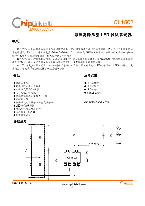
CL1502LED驱动
推荐工作范围
符号 ILED_1 ILED_2 VLED_MIN
参数
LED输出电流@Vout=72V (输入电压175V~265V) LED输出电流@Vout=36V (输入电压175V~265V)
最低LED负载电压
参数范围 单位
<220
mA
<300
mA
>15
V
CL1502_CN Rev. 1.1
4
PN结到环境的热阻
188 ℃/W
工作结温范围
-40℃ to 150 ℃
最低/最高存储温度
-55℃ to 150 ℃
CL1502
封装耗散等级
封装 SOP8
RθJA (℃/W) 188
注:超出“最大额定值”可能损毁器件。推荐工作范围内器件可以工作,但不保证其特性。运行在最大额定条件下
长时间可能会影响器件的可靠性。
其中,VIN为系统经过整流桥后的输入电压;L系统工作电感;VLED为LED灯上的工作压降。 在功率管关断时,电感电流开始下降。功率管关断时间公式为:
储能电感选取值为:
tOFF
=
L ×IPEAK VLED
L = VLED × (VIN - VLED ) f ×IPAEK × VIN
CL1502内部设置了功率管的最小关断时间和最大关断时间,分别为4.5us和240us。如果储能电感的感值很
CL1502具有多种恒流辅助功能,实现优异的线性补偿和高精度恒流效果。CL1502工作于电感电流临界连续 模式(TM),输出电流不随电感和负载的变化而变化,具有优异的负载调整特性。
CL1502集成多种保护功能,极大的增强了系统的可靠性。保护功能包括LED开路保护、LED短路保护、欠 压锁定,电流采样电阻短路保护和过温调节功能。
EUCHIPS EUCP50XY-1WxxxxC-0MWWZ LED 恒流调光驱动器 产品说明书

SHANGHAI EUCHIPS INDUSTRIAL CO.,LTDEUCP50XY-1WxxxxC-0MWWZProduct FeaturesLED 恒流调光驱动器概述EUCP50XY-1WxxxxC-0MWWZ 系列是恒流模式输出的LED 驱动器,抗浪涌等级高,防护等级为IP67,适用于户外。
用户可根据调光方式和市场需求选择相应的型号,并可通过NFC 编程器修改输出电流。
电源电压: 100-277VAC 或 141-391VDC 10kV 浪涌等级- 60℃低温启动(可选择) 100,000小时的寿命@ Tc=75C 5 年保修 @ Tc<=80C Airset TM NFC 编程电流输出精度+/-2% (可编程模型) 0-10V/PWM/DALI 可调光 (取决于型号) 调灭后待机功耗0.5W(取决于型号)电源控制器与风扇的辅助电源为12V 300mA (取决于型号) 输入过压保护(可选择)UL Class P , Class 2,ENEC/CB/CCC,SELV 认证 安全依据EN 61347-1, 61347-2-3,61347-2-13, 62384 应用 :LED 灯带、景观灯、工矿灯、路灯、泛光灯上海欧切斯实业有限公司型号清单 技术参数上海欧切斯实业有限公司注: 除非特别注明,所有的测试结果均在220VAC ,25℃室温下测得。
* 可选择标记项目,获取详细功能请联系销售人员调光安规/电磁兼容调调光光曲曲线线a. 带调灭功能默认值)b. 无调灭功能(联系销售获取此功能调光接线图(End of Life: Maximum Failure Rate=10%)使用寿命 vs. 外壳温度功率因数vs.负载THD vs.负载EUCP50NN(FR)-1WxxxxC-0MWWUUnspecified tolerance :±1AC INPUT(UL SJTW 3×18AWG)DC OUTPUT(UL SJTW 2×18AWG)BLACK(ACL)WHITE(ACN)GREEN(GND)RED(V+)BLUE(V-)效率 vs.负载 (1050mA)尺寸 (mm)EUCP50AR(AN)-1WxxxxC-0MWWUUnspecified tolerance :±1AC INPUT(UL SJTW 3×18AWG)DC OUTPUT(UL SJTW 2×18AWG)DIMMING WIRE(UL SJTW 2×18AWG)BLACK(ACL)WHITE(ACN)GREEN(GND)PURPLE(Vdim+)GRAY(Vdim-)RED(V+)BLUE(V-)EUCP50ER-1WxxxxC-0MWWUUnspecified tolerance :±1AC INPUT(UL SJTW 3×18AWG)DC OUTPUT(UL SJTW 2×18AWG)DIMMING WIRE(UL SJTW 3×18AWG)BLACK(ACL)WHITE(ACN)GREEN(GND)BLACK&WHITE(Vaux/+12V)PURPLE(Vdim+)GRAY(Vdim-)RED(V+)BLUE(V-)EUCP50DR-1WxxxxC-0MWWUUnspecified tolerance :±1AC INPUT(UL SJTW 3×18AWG)DC OUTPUT(UL SJTW 2×18AWG)DIMMING WIRE(UL 2464 4×22AWG)BLACK(ACL)WHITE(ACN)GREEN(GND)RED(V+)BLUE(V-)PINK(DALI 2)BLACK&WHITE(Vaux+)GRAY(Vaux-)BLUE&WHITE(DALI 1)EUCP50NN(FR)-1WxxxxC-0MWWSUnspecified tolerance :±1AC INPUT(VDE H05RN-F 3×1.0mm2)DC OUTPUT(VDE H05RN-F 2×1.0mm2)BROWN(ACL)BLUE(ACN)YELLOW&GREEN (GND)BROWN(V+)BLUE(V-)EUCP50AR(AN)-1WxxxxC-0MWWSUnspecified tolerance :±1AC INPUT(VDE H05RN-F 3×1.0mm2)DC OUTPUT(VDE H05RN-F 2×1.0mm2)DIMMING WIRE(H05RN-F 2×0.75mm2)BROWN(ACL)BLUE(ACN)YELLOW&GREEN (GND)PURPLE(Vdim+)GRAY(Vdim-)BROWN(V+)BLUE(V-)EUCP50ER-1WxxxxC-0MWWSUnspecified tolerance :±1AC INPUT(VDE H05RN-F 3×1.0mm2)DC OUTPUT(VDE H05RN-F 2×1.0mm2)DIMMING WIRE(H05RN-F 3×0.75mm2)BROWN(ACL)BLUE(ACN)YELLOW&GREEN (GND)BLACK&WHITE(Vaux/+12V)PURPLE(Vdim+)GRAY(Vdim-)BROWN(V+)BLUE(V-)EUCP50DR-1WxxxxC-0MWWSUnspecified tolerance :±1AC INPUT(VDE H05RN-F 3×1.0mm2)DC OUTPUT(VDE H05RN-F 2×1.0mm2)DIMMING WIRE(H05RN-F 4×0.5mm2)BROWN(ACL)BLUE(ACN)YELLOW&GREEN (GND)BROWN(V+)BLUE(V-)PINK(DALI 2)BLACK&WHITE(Vaux+)GRAY(Vaux-)BLUE&WHITE(DALI 1)。
LTC6401IUD-26#PBF中文资料

1640126fFREQUENCY (MHz)O U T P U T I P3 (d B m )10203040506050100150200640126 TA01bTYPICAL APPLICATIONFEATURESAPPLICATIONSDESCRIPTIONLow Distortion Differential ADC Driver for DC-140MHzThe LTC ®6401-26 is a high-speed differential amplifi er targeted at processing signals from DC to 140MHz. The part has been specifi cally designed to drive 12-, 14- and 16-bit ADCs with low noise and low distortion, but can also be used as a general-purpose broadband gain block.The LTC6401-26 is easy to use, with minimal support circuitry required. The output common mode voltage is set using an external pin, independent of the inputs, which eliminates the need of transformers or AC-coupling ca-pacitors in many applications. The gain is internally fi xed at 26dB (20V/V).The LTC6401-26 saves space and power compared to alternative solutions using IF gain blocks and transform-ers. The LTC6401-26 is packaged in a compact 16-lead 3mm × 3mm QFN package and operates over the –40°C to 85°C temperature range.Equivalent OIP3 vs Frequency■1.6GHz –3dB Bandwidth ■ Fixed Gain of 20V/V (26dB)■ –85dBc IMD3 at 70MHz (Equivalent OIP3 = 46.5dBm)■ –72dBc IMD3 at 140MHz (Equivalent OIP3 = 40dBm)■ 1nV/√H z Internal Op Amp Noise■ 1.5nV/√H z Total Input Referred Noise ■ 6.8dB Noise Figure■ Differential Inputs and Outputs ■ 50Ω Input Impedance■ 2.85V to 3.5V Supply Voltage ■ 45mA Supply Current (135mW)■ 1V to 1.6V Output Common Mode, Adjustable ■ DC- or AC-Coupled Operation■Max Differential Output Swing 4.7V P-P■ Small 16-Lead 3mm × 3mm × 0.75mm QFN Package■Differential ADC Driver ■ Differential Driver/Receiver■ Single Ended to Differential Conversion ■ IF Sampling Receivers ■ SAW Filter InterfacingSingle-Ended to Differential ADC Driver at 140MHz IF0.1μV2640126fABSOLUTE MAXIMUM RATINGSSupply Voltage (V + – V –) ..........................................3.6V Input Current (Note 2) ..........................................±10mA Operating Temperature Range(Note 3) ...............................................–40°C to 85°C Specifi ed Temperature Range(Note 4) ...............................................–40°C to 85°C Storage Temperature Range ...................–65°C to 150°C Maximum Junction Temperature ..........................150°C(Note 1)161514135678TOP VIEW UD PACKAGE16-LEAD (3mm × 3mm) PLA S TIC QFN 9101117124321V +V OCM V +V –V –ENABLE V +V ––I N–I N+I N +I N–O U T–O U T F+O U T F+O U TT JMAX = 150°C, θJA = 68°C/W, θJC = 4.2°C/WEXPOSED PAD (PIN 17) IS V –, MUST BE SOLDERED TO PCBORDER INFORMATIONLEAD FREE FINISH TAPE AND REELPART MARKING*PACKAGE DESCRIPTIONSPECIFIED TEMPERATURE RANGE LTC6401CUD-26#PBF LTC6401CUD-26#TRPBF LCDG 16-Lead (3mm × 3mm) Plastic QFN 0°C to 70°C LTC6401IUD-26#PBFLTC6401IUD-26#TRPBF LCDG16-Lead (3mm × 3mm) Plastic QFN–40°C to 85°CConsult LTC Marketing for parts specifi ed with wider operating temperature ranges. *The temperature grade is identifi ed by a label on the shipping container.Consult LTC Marketing for information on non-standard lead based fi nish parts.For more information on lead free part marking, go to: /leadfree/ For more information on tape and reel specifi cations, go to: /tapeandreel/LTC6400 AND LTC6401 SELECTOR GUIDEPART NUMBER GAIN(dB)GAIN (V/V)Z IN (DIFFERENTIAL)(Ω)I CC (mA)LTC6401-88 2.540045LTC6401-20201020050LTC6401-2626205045LTC6400-20201020090LTC6400-2626205085In addition to the LTC6401 family of amplifi ers, a lower distortion LTC6400 family is available. The LTC6400 is pin compatible to the LTC6401, and has the same low noise performance. The low distortion of the LTC6400 comes at the expense of higher power consumption. Please refer to the separate LTC6400 data sheets for complete details. Other gain versions from 8dB to 14dB will follow.Please check each datasheet for complete details.PIN CONFIGURATIONDC ELECTRICAL CHARACTERISTICSSYMBOL PARAMETER CONDITIONS MIN TYP MAX UNITS Input/Output Characteristic (+IN, –IN, +OUT, –OUT, +OUTF, –OUTF)G DIFF Gain V IN = ±50mV Differential●252627dB TC GAIN Gain Temperature Drift V IN = ±50mV Differential●0.003dB/°C V SWINGMIN Output Swing Low Each Output, V IN = ±200mV Differential●0.090.15V V SWINGMAX Output Swing High Each Output, V IN = ±200mV Differential● 2.3 2.43V V OUTDIFFMAX Maximum Differential Output Swing1dB Compressed● 4.3 4.7V P-P I OUT Output Current Drive Each Output, V IN = ±200mV,V OUT > 2V P-P●10mA V OS Input Offset Voltage Differential●–2.5 2.5mV TCV OS Input Offset Voltage Drift Differential●1μV/°C I VRMIN Input Common Mode Voltage Range, MIN1V I VRMAX Input Common Mode Voltage Range, MAX 1.6V R INDIFF Input Resistance (+IN, –IN)Differential●42.55057.5ΩC INDIFF Input Capacitance (+IN, –IN)Differential, Includes Parasitic1pF R OUTDIFF Output Resistance (+OUT, –OUT)Differential●182532ΩR OUTFDIFF Filtered Output Resistance (+OUTF, –OUTF)Differential●85100115ΩC OUTFDIFF Filtered Output Capacitance (+OUTF, –OUTF)Differential, Includes Parasitic 2.7pF CMRR Common Mode Rejection Ratio Input Common Mode Voltage1.1V to1.4V●5075dB Output Common Mode ControlG CM Common Mode Gain V OCM = 1V to 1.6V1V/VV OCMMIN Output Common Mode Range, MIN●11.1VVV OCMMAX Output Common Mode Range, MAX●1.61.5VVV OSCM Common Mode Offset Voltage V OCM = 1.1V to 1.5V●–1515mV TCV OSCM Common Mode Offset Voltage Drift●3μV/°C IV OCM V OCM Input Current●515μA E N A B L E PinV IL E N A B L E Input Low Voltage●0.8V V IH E N A B L E Input High Voltage● 2.4V I IL E N A B L E Input Low Current E N A B L E = 0.8V●0.5μA I IH E N A B L E Input High Current E N A B L E = 2.4V● 1.43μA Power SupplyV S Operating Supply Range● 2.853 3.5V I S Supply Current E N A B L E = 0V, Both Inputs andOutputs Floating●354560mAI SHDN Shutdown Supply Current E N A B L E = 3V, Both Inputs andOutputs Floating●0.83mAPSRR Power Supply Rejection Ratio (DifferentialOutputs)2.85V to 3.5V●6095.5dBThe● denotes the specifi cations which apply over the full operating temperature range, otherwise specifi cations are at T A = 25°C. V+ = 3V, V– = 0V, +IN = –IN = V OCM = 1.25V, E N A B L E = 0V, No R L unless otherwise noted.3640126fAC ELECTRICAL CHARACTERISTICS Specifi cations are at TA = 25°C. V+ = 3V, V– = 0V, V OCM = 1.25V,E N A B L E = 0V, No R L unless otherwise noted.SYMBOL PARAMETER CONDITIONS MIN TYP MAX UNITS –3dBBW–3dB Bandwidth200mV P-P,OUT (Note 6) 1.2 1.6GHz 0.5dBBW Bandwidth for 0.5dB Flatness200mV P-P,OUT (Note 6)0.5GHz 0.1dBBW Bandwidth for 0.1dB Flatness200mV P-P,OUT (Note 6)0.22GHz 1/f1/f Noise Corner16kHz SR Slew Rate Differential V OUT = 2V Step (Note 6)3300V/μs t S1%1% Settling Time V OUT = 2V P-P (Note 6)3ns t OVDR Overdrive Recovery Time V OUT = 1.9V P-P (Note 6)19ns t ON Turn-On Time+OUT, –OUT Within 10% of Final Values93ns t OFF Turn-Off Time I CC Falls to 10% of Nominal140ns –3dBBW VOCM V OCM Pin Small Signal –3dB BW0.1V P-P at V OCM, Measured Single-Endedat Output (Note 6)14.7MHz 10MHz Input SignalHD2,10M/HD3,10M Second/Third Order Harmonic Distortion V OUT = 2V P-P , R L = 200Ω–95/–81dBcV OUT = 2V P-P , No R L–93/–96dBcIMD3,10M Third-Order Intermodulation(f1 = 9.5MHz f2 = 10.5MHz)V OUT = 2V P-P Composite, R L = 200Ω–80dBc V OUT = 2V P-P Composite, No R L–97dBcOIP3,10M Equivalent Third-Order Output InterceptPoint (f1 = 9.5MHz f2 = 10.5MHz)V OUT = 2V P-P Composite, No R L (Note 7)52.5dBm P1dB,10M1dB Compression Point R L = 375Ω (Notes 5, 7)17.3dBm NF10M Noise Figure R L = 375Ω (Note 5) 6.8dB e IN,10M Input Referred Voltage Noise Density Includes Resistors (Short Inputs) 1.5nV/√H z e ON,10M Output Referred Voltage Noise Density Includes Resistors (Short Inputs)30nV/√H z 70MHz Input SignalHD2,70M/HD3,70M Second/Third Order Harmonic Distortion V OUT = 2V P-P , R L = 200Ω–83/–66dBcV OUT = 2V P-P , No R L–86/–81dBcIMD3,70M Third-Order Intermodulation(f1 = 69.5MHz f2 = 70.5MHz)V OUT = 2V P-P Composite, R L = 200Ω–74dBc V OUT = 2V P-P Composite, No R L–85dBcOIP3,70M Equivalent Third-Order Output InterceptPoint (f1 = 69.5MHz f2 = 70.5MHz)V OUT = 2V P-P Composite, No R L (Note 7)46.5dBm P1dB,70M1dB Compression Point R L = 375Ω (Notes 5, 7)17.2dBm NF70M Noise Figure R L = 375Ω (Note 5) 6.7dB e IN,70M Input Referred Voltage Noise Density Includes Resistors (Short Inputs) 1.44nV/√H z e ON,70M Output Referred Voltage Noise Density Includes Resistors (Short Inputs)28.8nV/√H z4640126fAC ELECTRICAL CHARACTERISTICSNote 1: Stresses beyond those listed under Absolute Maximum Ratings may cause permanent damage to the device. Exposure to any Absolute Maximum Rating condition for extended periods may affect device reliability and lifetime.Note 2: Input pins (+IN, –IN) are protected by steering diodes to either supply. If the inputs go beyond either supply rail, the input current should be limited to less than 10mA.Note 3: The LTC6401C and LTC6401I are guaranteed functional over the operating temperature range of –40°C to 85°CNote 4: The LTC6401C is guaranteed to meet specifi ed performance from 0°C to 70°C. It is designed, characterized and expected to meet specifi ed performance from –40°C to 85°C but is not tested or QA sampled at these temperatures. The LTC6401I is guaranteed to meet specifi ed performance from –40°C to 85°C.Note 5: Input and output baluns used. See Test Circuit A.Note 6: Measured using Test Circuit B. R L = 87.5Ω per output.Note 7: Since the LTC6401-26 is a feedback amplifi er with low output impedance, a resistive load is not required when driving an AD converter. Therefore, typical output power is very small. In order to compare the LTC6401-26 with amplifi ers that require 50Ω output load, the output voltage swing driving a given R L is converted to OIP3 and P1dB as if it were driving a 50Ω load. Using this modifi ed convention, 2V P-P is by defi nition equal to 10dBm, regardless of actual R L.SYMBOL PARAMETER CONDITIONS MIN TYP MAX UNITS 140MHz Input SignalHD2,140M/ HD3,140M Second/Third Order Harmonic Distortion V OUT = 2V P-P , R L = 200Ω–81/–54dBcV OUT = 2V P-P , No R L–85/–69dBcIMD3,140M Third-Order Intermodulation(f1 = 139.5MHz f2 = 140.5MHz)V OUT = 2V P-P Composite, R L = 200Ω–64dBc V OUT = 2V P-P Composite, No R L–72dBcOIP3,140M Equivalent Third-Order Output InterceptPoint(f1 = 139.5MHz f2 = 140.5MHz)V OUT = 2V P-P Composite, No R L (Note 7)40dBm P1dB,140M1dB Compression Point R L = 375Ω (Notes 5, 7)17.4dBm NF140M Noise Figure R L = 375Ω (Note 5) 6.5dB e N,140M Input Referred Voltage Noise Density Includes Resistors (Short Inputs) 1.43nV/√H z e ON,140M Output Referred Voltage Noise Density Includes Resistors (Short Inputs)28.6nV/√H zIMD3,130M/150M Third-Order Intermodulation(f1 = 130MHz f2 = 150MHz)Measure at 170MHz V OUT = 2V P-P Composite, R L = 375Ω–70–62dBc Specifi cations are at T A = 25°C. V+ = 3V, V– = 0V, V OCM = 1.25V,E N A B L E = 0V, No R L unless otherwise noted.5640126f6640126fTYPICAL PERFORMANCE CHARACTERISTICSFrequency ResponseGain 0.1dB FlatnessS21 Phase and Group Delay vs FrequencyInput and Output Refl ection and Reverse Isoloation vs FrequencyInput and Output Impedance vs FrequencyPSRR and CMRR vs FrequencyFREQUENCY (MHz)10G A I N (d B )51015203010010003000640126 G0125FREQUENCY (MHz)10–1.0G A I N F L A T N E S S (d B )–0.6–0.20.20.610010003000640126 G021.0–0.8–0.400.40.8FREQUENCY (MHz)0P H A S E (D E G R E E )GROUP DELAY (ns )–100–50800640126 G03–150–20020040060010000.40.60.200.8FREQUENCY (MHz)10–70S P A R A M E T E R S (d B )–60–40–20–50–30–10010*********640126 G04FREQUENCY (MHz)10I M P E D A N C E M A G N I T U D E (Ω)PHASE (DEGREE)601201001000640126 G0518030901500102030406050FREQUENCY (MHz)1P S R R , C M R R(d B )80100120101001000640126 G066040207640126fFREQUENCY (MHz)N O I S E F I G U R E (d B )INPUT REFERRED NOISE VOLTAGE (n V/√Hz)98640126 G075762.01.501.00.5100010100TIME (ns )0O U T P U T V O L T A G E (V )1.251.308640126 G081.201.15246101.35TIME (ns )0O U T P U T V O L T A G E (V )1.52.02.516640126 G091.00.50481220TIME (ns )O U T P U T V O L T A G E (V )1.52.02.5200640126 G101.00.550100150250TIME (ns )S E T T L I N G (%)1354640126 G11–1–3024–2–4–51235FREQUENCY (MHz)–40–50–60–70–80–90–100–110150640126 G1250100200H A R M O N I C D I S T O R T I O N (d B c )TYPICAL PERFORMANCE CHARACTERISTICSOverdriven Transient Response1% Settling Time for 2V Output StepHarmonic Distortion vs FrequencyNoise Figure and Input Referred Noise Voltage vs FrequencySmall Signal Transient ResponseLarge Signal Transient Response8640126fFREQUENCY (MHz)–40–50–60–70–80–90–100–110150640126 G1350100200T H I R D O R D E R I M D (d B c )FREQUENCY (MHz)–40–50–60–70–80–90–100–110150640126 G1450100200H A R M O N I C D I S T O R T I O N (d B c )FREQUENCY (MHz)–40–50–60–70–80–90–100–110150640126 G1550100200T H I R D O R D E R I MD (d B c )FREQUENCY (MHz)016.0O U T P U T 1d B C O M P R E S S I O N P O I N T (d B m)16.517.017.518.018.519.050100150200640126 G16FREQUENCY (MHz)O U T P U T I P 3 (d B m )10203040506050100150200640126 G17TIME (ns )–100V O L T A G E (V )I CC (mA)1.01.52.0200400640126 G180.500–0.501003002.53.03.520304010–10506070500TIME (ns )–100V O L T A G E (V )I CC (mA)1.01.52.0200400640126 G190.500–0.501003002.53.03.520304010–10506070500TYPICAL PERFORMANCE CHARACTERISTICSThird Order Intermodulation Distortion vs FrequencyHarmonic Distortion vs FrequencyThird Order Intermodulation Distortion vs FrequencyOutput 1dB Compression Point vs FrequencyEquivalent Output Third Order Intercept Point vs FrequencyTurn-On TimeTurn-Off Time9640126fBLOCK DIAGRAMPIN FUNCTIONSV + (Pins 1, 3, 10): Positive Power Supply (Normally tied to 3V or 3.3V). All three pins must be tied to the same voltage. Bypass each pin with 1000pF and 0.1μF capaci-tors as close to the pins as possible.V OCM (Pin 2): This pin sets the output common mode voltage. An 0.1μF external bypass capacitor is recom-mended.V – (Pins 4, 9, 12, 17): Negative Power Supply. All four pins must be connected to same voltage/ground.–OUT, +OUT (Pins 5, 8): Unfi ltered Outputs. These pins have series 12.5Ω resistors R OUT .–OUTF, +OUTF (Pins 6, 7): Filtered Outputs. These pins have 50Ω series resistors and a 2.7pF shunt capacitor.E N A B L E (Pin 11): This pin is a logic input referenced to V EE . If low, the part is enabled. If high, the part is disabled and draws very low standby current while the internal op amp has high output impedance.+IN (Pins 13, 14): Positive Input. Pins 13 and 14 are internally shorted together.–IN (Pins 15, 16): Negative Input. Pins 15 and 16 are internally shorted together.Exposed Pad (Pin 17): V –. The Exposed Pad must be connected to same voltage/ground as pins 4, 9, 12.APPLICATIONS INFORMATIONCircuit OperationThe LTC6401-26 is a low noise and low distortion fully differential op amp/ADC driver with:• Operation from DC to 1.6GHz –3dB bandwidth• Fixed gain of 20V/V (26dB)• Differential input impedance 50Ω• Differential output impedance 25Ω• Differential impedance of output fi lter 100ΩThe LTC6401-26 is composed of a fully differential amplifi er with on chip feedback and output common mode voltage control circuitry. Differential gain and input impedance are set by 25Ω/500Ω resistors in the feedback network. Small output resistors of 12.5Ω improve the circuit stability over various load conditions. They also provide a possible external fi ltering option, which is often desirable when the load is an ADC.Filter resistors of 50Ω are available for additional fi ltering. Lowpass/bandpass fi lters are easily implemented with just a couple of external components. Moreover, they offer single-ended 50Ω matching in wideband applications and no external resistor is needed.The LTC6401-26 is very fl exible in terms of I/O coupling. It can be AC- or DC-coupled at the inputs, the outputs or both. Due to the internal connection between input and output, users are advised to keep input common mode voltage between 1V and 1.6V for proper operation. If the inputs are AC-coupled, the input common mode voltage is automatically biased close to V OCM and thus no external circuitry is needed for bias. The LTC6401-26 provides an output common mode voltage set by V OCM, which allows driving ADC directly without external components such as transformer or AC coupling capacitors. The input signal can be either single-ended or differential with only minor difference in distortion performance.Input Impedance and MatchingThe differential input impedance of the LTC6401-26 is 50Ω. The interface between the input of LTC6401-26 and 50Ωsource is straightforward. One way is to directly connect them if the source is differential (Figure 1). Another ap-proach is to employ a wideband transformer if the source is single ended (Figure 2). Both methods provide a wide-band match. Alternatively, one could apply a narrowband impedance match at the inputs of the LTC6401-26 for frequency selection and/or noise reduction.Referring to F igure 3, LTC6401-26 can be easily confi gured for single-ended input and differential output without a balun. The signal is fed to one of the inputs through a matching network while the other input is connected to the same matching network and a source resistor. Because the return ratios of the two feedback paths are equal, the two outputs have the same gain and thus symmetrical swing. In general, the single-ended input impedance and termination resistor R T are determined by the combination of R S, R G and R F. For example, when R S is 50Ω, it is found that the single-ended input impedance is 75Ω and R T is 150Ω in order to match to a 50Ω source impedance.Figure 1. Input Termination for Differential 50Ω Input ImpedanceFigure 2. Input Termination for Differential 50Ω Input Impedance Using a Balun10640126f11640126fThe LTC6401-26 is unconditionally stable, i.e. differential stability factor Kf>1 and stability measure B1>0. However, the overall differential gain is affected by both source impedance and load impedance as shown in Figure 4:A V V R R R V OUT IN S L L==++10005025•The noise performance of the LTC6401-26 also dependsupon the source impedance and termination. A trade-off between gain and noise is obvious when constant noise fi gure circle and constant gain circle are plotted within the same input Smith Chart, based on which users can choose the optimal source impedance for a given gain and noise requirement.Output Impedance Match and FilterThe LTC6401-26 can drive an ADC directly without external output impedance matching. Alternatively, the differential output impedance of 25Ω can be made larger, e.g. 50Ω, by series resistors or LC network.Figure 4. Calculate Differential GainAPPLICATIONS INFORMATIONFigure 3. Input Termination for Single-Ended 50Ω Input ImpedanceThe internal low pass fi lter outputs at +OUTF/–OUTF have a –3dB bandwidth of 590MHz. External capacitors can reduce the low pass fi lter bandwidth as shown in Figure 5. A bandpass fi lter is easily implemented with only a few components as shown in Figure 6. Three 39pF ca-pacitors and 16nH inductor create a bandpass fi lter with 165MHz center frequency, –3dB frequencies at 138MHz and 200MHz.Output Common Mode AdjustmentThe LTC6401-26’s output common mode voltage is set by the V OCM pin, which is a high impedance input. The output common mode voltage is capable of tracking V OCM in a range from 1V to 1.6V. Bandwidth of V OCM control is typically 15MHz, which is dominated by a low pass fi lter connected to the V OCM pin and is aimed to reduce com-mon mode noise generation at the outputs. The internal common mode feedback loop has a –3dB bandwidth of 400MHz, allowing fast rejection of any common mode output voltage disturbance. The V OCM pin should be tied to a DC bias voltage with a 0.1μF bypass capacitor. When interfacing with 3V A/D converters such as the LTC22xx families, the V OCM pin can be connected to the V CM pin of the ADC.Driving A/D ConvertersThe LTC6401-26 has been specifi cally designed to interface directly with high speed A/D converters. F igure 7 shows the LTC6401-26 with single-ended input driving the LTC2208, which is a 16-bit, 130Msps ADC. Two external 5Ω resistors help eliminate potential resonance associated with bond wires of either the ADC input or the driver output. V OCMFigure 5. LTC6401-26 Internal Filter Topology Modifi ed for Low Filter Bandwidth (Three External Capacitors)Figure 6. LTC6401-26 with 165MHz Output Bandpass Filter Figure 7. Single-Ended Input to LTC6401-26 and LTC2208Figure 8. IMD3 for the Combination of LTC6401-26 and LTC2208of the LTC6401-26 is connected to V CM of the LTC2208 at 1.25V. Alternatively, a single-ended input signal can be converted to a differential signal via a balun and fed to the input of the LTC6401-26. Figure 8 summarizes the IMD3 performance of the whole system as shown in Figure 7. Test CircuitsDue to the fully-differential design of the LTC6401 and its usefulness in applications with differing characteristic specifi cations, two test circuits are used to generate the information in this datasheet. Test Circuit A is DC987B, a two-port demonstration circuit for the LTC6401 family. The silkscreen is shown in Figure 9. This circuit includes input and output transformers (baluns) for single-ended-to-differential conversion and impedance transformation, allowing direct hook-up to a 2-port network analyzer. There are also series resistors at the output to present the LTC6401 with a 375Ω differential load, optimizing distortion performance. Due to the input and output transformers, the –3dB bandwidth is reduced from 1.6GHz to 1.37GHz.Test Circuit B uses a 4-port network analyzer to measure S-parameters and gain/phase response. This removes the effects of the wideband baluns and associated circuitry, for a true picture of the >1GHz S-parameters and AC characteristics.APPLICATIONS INFORMATIONFigure 9. Top Silkscreen for DC987B, Test Circuit AFREQUENCY (MHz)–40–50–60–70–80–90–100–110150640126 F0850100200IMD3(dBc)12640126f13640126fTYPICAL APPLICATIONDemo Circuit 987B Schematic (Test Circuit A)VERSIONIC R3R4T1SL1SL2SL3-HLTC6401UD-26OPEN OPENM/A-COM MABA-007159-0000000dB20dB14dB640126 TA02J5–OUTS L3(2)J4+OUT TP2V CC2.85V TO3.5VμFTP5V OCMTE S J7TE S T OUTNOTE: UNLE SS OTHERWI S E S PECIFIED.(1) DO NOT S TUFF.(2)S L = S IGNAL LEVELTP3GNDTYPICAL APPLICATIONTest Circuit B, 4-Port Analysis+14640126f15640126fInformation furnished by Linear Technology Corporation is believed to be accurate and reliable. However, no responsibility is assumed for its use. Linear Technology Corporation makes no representa-tion that the interconnection of its circuits as described herein will not infringe on existing patent rights.PACKAGE DESCRIPTIONRECOMMENDED S OLDER PAD PITCH AND DIMEN S ION SNOTE:1. DRAWING CONFORM S TO JEDEC PACKAGE OUTLINE MO-220 VARIATION (WEED-2)2. DRAWING NOT TO S CALE3. ALL DIMEN S ION S ARE IN MILLIMETER S4. DIMEN S ION S OF EXPO S ED PAD ON BOTTOM OF PACKAGE DO NOT INCLUDEMOLD FLA S H. MOLD FLA S H, IF PRE S ENT, S HALL NOT EXCEED 0.15mm ON ANY S IDE 5. EXPO S ED PAD S HALL BE S OLDER PLATED6. S HADED AREA I S ONLY A REFERENCE FOR PIN 1 LOCATION ON THE TOP AND BOTTOM OF PACKAGEBOTTOM VIEW—EXPO S ED PAD × 45° CHAMFERUD Package16-Lead Plastic QFN (3mm × 3mm)(Reference LTC DWG # 05-08-1691)16640126fLinear Technology Corporation1630 McCarthy Blvd., Milpitas, CA 95035-7417(408) 432-1900 ● FAX: (408) 434-0507 ● © LINEAR TECHNOLOGY CORPORA TION 2008LT 0108 • PRINTED IN USARELATED PARTSPART NUMBER DESCRIPTIONCOMMENTSHigh-Speed Differential Amplifi ers/Differential Op AmpsLT ®1993-2800MHz Differential Amplifi er/ADC Driver A V = 2V/V, OIP3 = 38dBm at 70MHz LT1993-4900MHz Differential Amplifi er/ADC Driver A V = 4V/V, OIP3 = 40dBm at 70MHz LT1993-10700MHz Differential Amplifi er/ADC Driver A V = 2V/V, OIP3 = 40dBm at 70MHzLT1994Low Noise, Low Distortion Differential Op Amp 16-Bit SNR and SFDR at 1MHz, Rail-to-Rail OutputsLT5514Ultralow Distortion IF Amplifi er/ADC Driver with Digitally Controlled GainOIP3 = 47dBm at 100MHz, Gain Control Range 10.5dB to 33dB LT5524Low Distortion IF Amplifi er/ADC Driver with Digitally Controlled GainOIP3 = 40dBm at 100MHz, Gain Control Range 4.5dB to 37dB LTC6400-20 1.8GHz Low Noise, Low Distortion, Differential ADC Driver A V = 20dB, 90mA Supply Current, IMD3 = –65dBc at 300MHz LTC6400-26 1.9GHz Low Noise, Low Distortion, Differential ADC Driver A V = 26dB, 85mA Supply Current, IMD3 = –71dBc at 300MHz LTC6401-8 2.2GHz Low Noise, Low Distortion, Differential ADC Driver A V = 8dB, 45mA Supply Current, IMD3 = –80dBc at 140MHz LTC6401-20 1.3GHz Low Noise, Low Distortion, Differential ADC Driver A V = 20dB, 50mA Supply Current, IMD3 = –74dBc at 140MHz LT6402-6300MHz Differential Amplifi er/ADC Driver A V = 6dB, Distortion < –80dBc at 25MHz LT6402-12300MHz Differential Amplifi er/ADC Driver A V = 12dB, Distortion < –80dBc at 25MHz LT6402-20300MHz Differential Amplifi er/ADC Driver A V = 20dB, Distortion < –80dBc at 25MHzLTC64063GHz Rail-to-Rail Input Differential Op Amp1.6nV/√H z Noise, –72dBc Distortion at 50MHz, 18mALT6411Low Power Differential ADC Driver/Dual Selectable Gain Amplifi er16mA Supply Current, IMD3 = –83dBc at 70MHz, A V = 1, –1 or 2High-Speed Single-Ended Output Op AmpsLT1812/LT1813/LT1814High Slew Rate Low Cost Single/Dual/Quad Op Amps8nV/√H z Noise, 750V/μs, 3mA Supply Current LT1815/LT1816/LT1817Very High Slew Rate Low Cost Single/Dual/Quad Op Amps 6nV/√H z Noise, 1500V/μs, 6.5mA Supply Current LT1818/LT1819Ultra High Slew Rate Low Cost Single/Dual Op Amps 6nV/√H z Noise, 2500V/μs, 9mA Supply CurrentLT6200/LT6201Rail-to-Rail Input and Output Low Noise Single/Dual Op Amps0.95nV/√H z Noise, 165MHz GBW, Distortion = –80dBc at 1MHz LT6202/LT6203/LT6204Rail-to-Rail Input and Output Low Noise Single/Dual/Quad Op Amps 1.9nV/√H z Noise, 3mA Supply Current, 100MHz GBW LT6230/LT6231/LT6232Rail-to-Rail Output Low Noise Single/Dual/Quad Op Amps 1.1nV/√H z Noise, 3.5mA Supply Current, 215MHz GBW LT6233/LT6234/LT6235Rail-to-Rail Output Low Noise Single/Dual/Quad Op Amps 1.9nV/√H z Noise, 1.2mA Supply Current, 60MHz GBWIntegrated Filters LTC1562-2Very Low Noise, 8th Order Filter Building Block Lowpass and Bandpass Filters up to 300kHz LT1568Very Low Noise, 4th Order Filter Building Block Lowpass and Bandpass Filters up to 10MHz LTC1569-7Linear Phase, Tunable 10th Order Lowpass Filter Single-Resistor Programmable Cut-Off to 300kHz LT6600-2.5Very Low Noise Differential 2.5MHz Lowpass Filter SNR = 86dB at 3V Supply, 4th Order Filter LT6600-5Very Low Noise Differential 5MHz Lowpass Filter SNR = 82dB at 3V Supply, 4th Order Filter LT6600-10Very Low Noise Differential 10MHz Lowpass Filter SNR = 82dB at 3V Supply, 4th Order Filter LT6600-15Very Low Noise Differential 15MHz Lowpass Filter SNR = 76dB at 3V Supply, 4th Order Filter LT6600-20Very Low Noise Differential 20MHz Lowpass FilterSNR = 76dB at 3V Supply, 4th Order Filter。
Linear Technology LTC6363 系列精密、低功耗差分放大器 ADC 驱动器系列说

LTC6363 系列精密、低功耗差分放大器/ADC 驱动器系列特点⏹提供用户设置增益或0.5V/V、1V/V、2V/V的固定增益⏹折合到输入端噪声:2.9nV/√Hz⏹电源电流:2mA(最大值)⏹增益误差:45ppm(最大值)⏹增益误差漂移:0.5ppm/°C(最大值)⏹CMRR:94dB(最小值)⏹失调电压:100µV(最大值)⏹输入失调电流:50nA(最大值)⏹快速建立时间:720ns 至18 位,8V P–P输出⏹电源电压范围:2.8V (±1.4V) 至11V (±5.5V) ⏹差分轨到轨输出⏹输入共模范围包含地⏹低失真:115dB SFDR,2kHz 时,18V P–P⏹增益带宽积:500MHz⏹–3dB 带宽:35MHz⏹低功耗关断:20µA (V S = 3V)⏹8 引脚MSOP 和2 mm × 3mm 8 引脚DFN 封装应用⏹20 位、18 位和16 位SAR ADC 驱动器⏹单端至差分转换⏹低功耗ADC 驱动器⏹电平转换器⏹差分线路驱动器⏹电池供电仪器仪表说明LTC®6363系列包括四款全差分、低功耗、低噪声放大器,提供轨到轨输出,针对SAR ADC 驱动进行了优化。
LTC6363 是一款独立的差分放大器,其增益通常利用四个外部电阻设置。
LTC6363–0.5、LTC6363–1 和LTC6363–2 均有内部匹配电阻,形成增益分别为0.5V/V、1V/V 和2V/V 的固定增益模块。
每个固定增益放大器都有激光调整的精密片内电阻,可实现精确、超稳定的增益和出色的CMRR。
系列选型表产品型号增益配置LTC6363 用户设置LTC6363–0.5 0.5V/VLTC6363–1 1V/VLTC6363–22V/V所有注册商标和商标均属各自所有人所有。
典型应用从以地为基准的单端输入到LTC2378–20 SAR ADC 的直流耦合接口LTC6363–1 驱动LTC2378–20f IN = 2kHz,–1dBFS,131k 点FFTLTC6363 系列 绝对最大额定值(注释 1)总电源电压 (V + – V –) ........................................... 12V 输入电压(+IN 、–IN )(注释 2)LTC6363–0.5 ........ (V –) – 14.9V 至 (V +) + 14.9V LTC6363–1 ........... (V –) – 11.1V 至 (V +) + 11.1V LTC6363–2 ........... (V –) – 7.45V 至 (V +) + 7.45V 输入电流(+IN 、–IN )LTC6363(注释 3)............................................................................. ±10mA 输入电流(V OCM 、SHDN )(注释 3) .................................................. ±10mA 输出短路持续时间(注释 4) ......................................... 受散热限制 工作温度范围(注释 5)LTC6363I/LTC6363I–0.5/LTC6363I–1/ LTC6363I–2 ................................... –40°C 至 85°C LTC6363H/LTC6363H–0.5/LTC6363H–1/LTC6363H–2 ............................... –40°C 至 125°C 额定温度范围(注释 6)LTC6363I/LTC6363I–0.5/LTC6363I–1/LTC6363I–2 .................................. –40°C 至 85°C LTC6363H/LTC6363H–0.5/LTC6363H–1/LTC6363H–2............................... –40°C 至 125°C 最高结温 .............................................................. 150°C 存储温度范围 .................................. –65°C 至 150°C MSOP 引脚温度(焊接,10 秒) ................ 300°C引脚配置LTC6363LTC6363LTC6363–0.5/LTC6363–1/LTC6363–2订购信息 /product/LTC6363#orderinfo管装卷带和卷盘 器件标识* 封装说明温度范围 LTC6363IMS8#PBF LTC6363IMS8#TRPBF LTGSQ 8 引脚塑料 MSOP –40°C 至 85°C LTC6363HMS8#PBFLTC6363HMS8#TRPBFLTGSQ8 引脚塑料 MSOP –40°C 至 125°C LTC6363IMS8–0.5#PBF LTC6363IMS8–0.5#TRPBF LTGST 8 引脚塑料 MSOP –40°C 至 85°C LTC6363HMS8–0.5#PBF LTC6363HMS8–0.5#TRPBF LTGST 8 引脚塑料 MSOP –40°C 至 125°C LTC6363IMS8–1#PBF LTC6363IMS8–1#TRPBF LTGSR 8 引脚塑料 MSOP –40°C 至 85°C LTC6363HMS8–1#PBF LTC6363HMS8–1#TRPBF LTGSR 8 引脚塑料 MSOP –40°C 至 125°C LTC6363IMS8–2#PBF LTC6363IMS8–2#TRPBF LTGSS 8 引脚塑料 MSOP –40°C 至 85°C LTC6363HMS8–2#PBFLTC6363HMS8–2#TRPBFLTGSS8 引脚塑料 MSOP–40°C 至 125°CLTC6363 系列订购信息无铅表面处理卷带和卷盘(迷你型)卷带和卷盘器件标识*封装说明温度范围LTC6363IDCB#TRMPBF LTC6363IDCB#TRPBF LGVG 8 引脚(2mm × 3mm) 塑料DFN –40°C 至85°CLTC6363HDCB#TRMPBF LTC6363HDCB#TRPBF LGVG 8 引脚(2mm × 3mm) 塑料DFN –40°C 至125°CTRM = 500 片。
18V 4 pc Combo Cordless Tool Kit 8083362 用户手册说明书

For any technical questions, please call 1-800-665-8685 2
For any technical questions, please call 1-800-665-8685 4
Detail sander parts identification
a) On/off trigger b) Handle c) Sanding plate d) Hook and loop sanding pad e) Battery pack location
For any technical questions, please call 1-800-665-8685 3
Flashlight Operation
• Insert battery into flashlight slot and secure. • Slide the switch on the handle to 1 of the 2 brightness positions. • Slide the switch to the off position to turn off.
• To charge the battery, insert the battery pack in the charger. Plug the charger into a power outlet and press the ‘set’ button on the charger.
LTC4213 1 4213f 电子电路保护器说明书

2µs/DIV4213 TA01b124213fBias Supply Voltage (V CC )...........................–0.3V to 9V Input VoltagesON, SENSEP, SENSEN.............................–0.3V to 9V I SEL ..........................................–0.3V to (V CC + 0.3V)Output VoltagesGATE .....................................................–0.3V to 15V READY.....................................................–0.3V to 9V Operating Temperature RangeLTC4213C ...............................................0°C to 70°C LTC4213I.............................................–40°C to 85°C Storage Temperature Range.................–65°C to 150°C Lead Temperature (Soldering, 10sec)...................300°CORDER PART NUMBER DDB PART*MARKING T JMAX = 125°C, θJA = 250°C/WEXPOSED PAD (PIN 9)PCB CONNECTION OPTIONALConsult LTC Marketing for parts specified with wider operating temperature ranges.*The temperature grade is identified by a label on the shipping container.LBHVLTC4213CDDB LTC4213IDDB ABSOLUTE AXI U RATI GSW W WU PACKAGE/ORDER I FOR ATIOUUW (Note 1)ELECTRICAL CHARACTERISTICSThe ● denotes the specifications which apply over the full operatingtemperature range, otherwise specifications are at T A = 25°C. V CC = 5V, I SEL = 0 unless otherwise noted. (Note 2)SYMBOL PARAMETER CONDITIONSMIN TYP MAX UNITSV CC Bias Supply Voltage ● 2.36V V SENSEP SENSEP Voltage ●06V I CC V CC Supply Current●1.63mA V CC(UVLR)V CC Undervoltage Lockout Release V CC Rising● 1.8 2.07 2.23V ∆V CC(UVHYST)V CC Undervoltage Lockout Hysteresis ●30100160mV I SENSEP SENSEP Input Current V SENSEP = V SENSEN = 5V, Normal Mode 154080µA V SENSEP = V SENSEN = 0, Normal Mode –1±15µA I SENSENSENSEN Input CurrentV SENSEP = V SENSEN = 5V, Normal Mode 154080µA V SENSEP = V SENSEN = 0, Normal Mode –1±15µA V SENSEP = V SENSEN = 5V,50280µAReset Mode or Fault ModeV CBCircuit Breaker Trip Voltage I SEL = 0, V SENSEP = V CC●22.52527.5mV V CB = V SENSEP – V SENSEN I SEL = Floated, V SENSEP = V CC ●455055mV I SEL = V CC, V SENSEP = V CC ●90100110mV V CB(FAST)Fast Circuit Breaker Trip Voltage I SEL = 0, V SENSEP = V CC●63100115mV V CB(FAST)= V SENSEP – V SENSEN I SEL = Floated, V SENSEP = V CC ●126175200mV I SEL = V CC, V SENSEP = V CC ●252325371mV I GATE(UP)GATE Pin Pull Up Current V GATE = 0V●–50–100–150µA I GATE(DN)GATE Pin Pull Down Current ∆V SENSEP – V SENSEN = 200mV, V GATE = 8V ●1040mA ∆V GSMAX External N-Channel Gate Drive V SENSEN = 0, V CC ≥ 2.97V, I GATE = –1µA ● 4.8 6.58V V SENSEN = 0, V CC = 2.3V, I GATE = –1µA ● 2.65 4.38V ∆V GSARMV GS Voltage to Arm Circuit BreakerV SENSEN = 0, V CC ≥ 2.97V ● 4.4 5.47.6V V SENSEN = 0, V CC = 2.3V●2.53.57VTOP VIEWDDB PACKAGE8-LEAD (3mm × 2mm) PLASTIC DFN567894321READY ON I SEL GND V CC SENSEP SENSEN GATE34213f∆V GSMAX – ∆V GSARM Difference Between ∆V GSMAX and V SENSEN = 0, V CC ≥ 2.97V ●0.3 1.1V ∆V GSARMV SENSEN = 0, V CC = 2.3V●0.150.8VV READY(OL)READY Pin Output Low Voltage I READY = 1.6mA, Pull Down Device On ●0.20.4V I READY(LEAK)READY Pin Leakage Current V READY = 5V, Pull Down Device Off ●0±1µA V ON(TH)ON Pin High Threshold ON Rising, GATE Pulls Up ●0.760.80.84V ∆V ON(HYST)ON Pin Hysteresis ON Falling, GATE Pulls Down104090mV V ON(RST)ON Pin Reset Threshold ON Falling, Fault Reset, GATE Pull Down ●0.360.40.44V I ON(IN)ON Pin Input Current V ON = 1.2V●0±1µA ∆V OV Overvoltage Threshold ●0.410.7 1.1V ∆V OV = V SENSEP – V CCt OVOvervoltage Protection Trip Time V SENSEP = V SENSEN = Step 5V to 6.2V 2565160µs t FAULT(SLOW)V CB Trips to GATE Discharging ∆V SENSE Step 0mV to 50mV,●71627µs V SENSEN Falling, V CC = V SENSEP = 5V t FAULT(FAST)V CB(FAST) Trips to GATE Discharging ∆V SENSE Step 0V to 0.3V, V SENSEN Falling,●12.5µs V SENSEP = 5Vt DEBOUNCE Startup De-Bounce Time V ON = 0V to 2V Step to Gate Rising,2760130µs (Exiting Reset Mode)t READY READY Delay Time V GATE = 0V to 8V Step to READY Rising,2250115µs V SENSEP = V SENSEN = 0t OFF Turn-Off Time V ON = 2V to 0.6V Step to GATE Discharging 1.5510µs t ON Turn-On Time V ON = 0.6V to 2V Step to GATE Rising,4816µs (Normal Mode)t RESETReset TimeV ON Step 2V to 0V2080150µsNote 1: Absolute Maximum Ratings are those values beyond which the life of a device may be impaired.ELECTRICAL CHARACTERISTICSThe ● denotes the specifications which apply over the full operatingtemperature range, otherwise specifications are at T A = 25°C. V CC = 5V, I SEL = 0 unless otherwise noted. (Note 2)SYMBOLPARAMETERCONDITIONSMIN TYP MAX UNITSNote 2: All currents into device pins are positive; all currents out of device pins are negative. All voltages are referenced to ground unless otherwise specified.4564213ft RESET vs Temperaturet FAULT(SLOW) vs V CCt FAULT(SLOW) vs Temperaturet FAULT(FAST) vs V CCt FAULT(FAST) vs TemperatureTYPICAL PERFOR A CE CHARACTERISTICSU WSpecifications are at T A = 25°C. V CC = 5Vunless otherwise noted.t F A U L T (F A S T ) (µs )4213 G230.90.80.71.01.11.21.3TEMPERATURE (°C)–50050100125–252575BIAS SUPPLY VOLTAGE (V)2.010t F A U L T (S L O W ) (µs )14121618 3.0 4.0 5.0 6.04213 G202022 2.53.54.55.5TEMPERATURE (°C)–500501001254213 G21–25257510t F A U L T (S L O W ) (µs )141216182022TEMPERATURE (°C)–500501001254213 G19–252575t R E S E T (µs )60708090100BIAS SUPPLY VOLTAGE (V)2.0t F A U L T (F A S T ) (µs )3.04.05.06.04213 G222.53.54.55.50.90.80.71.01.11.21.374213fPI FU CTIO SU U UREADY (Pin 1): READY Status Output. Open drain output that goes high impedance when the external MOSFET is on and the circuit breaker is armed. Otherwise this pin pulls low.ON (Pin 2): ON Control Input. The LTC4213 is in reset mode when the ON pin is below 0.4V. When the ON pin increases above 0.8V, the device starts up and the GATE pulls up with a 100µA current source. When the ON pin drops below 0.76V, the GATE pulls down. To reset a circuit breaker fault, the ON pin must go below 0.4V.I SEL (Pin 3): Threshold Select Input. With the I SEL pin grounded, float or tied to V CC the V CB is set to 25mV, 50mV or 100mV, respectively. The corresponding V CB(FAST)values are 100mV, 175mV and 325mV.GND (Pin 4): Device Ground.GATE (P in 5): GATE D rive Output. An internal charge pump supplies 100µA pull-up current to the gate of the external N-channel MOSFET. Internal circuitry limits thevoltage between the GATE and SENSEN pins to a safe gate drive voltage of less than 8V. When the circuit breaker trips, the GATE pin abruptly pulls to GND.SENSEN (Pin 6): Circuit Breaker Negative Sense Input.Connect this pin to the source of the external MOSFET.During reset or fault mode, the SENSEN pin discharges the output to ground with 280µA.SENSEP (P in 7): Circuit Breaker Positive Sense Input.Connect this pin to the drain of external N-channel MOSFET.The circuit breaker trips when the voltage across SENSEP and SENSEN exceeds V CB . The input common mode range of the circuit breaker is from ground to V CC + 0.2V when V CC < 2.5V. For V CC ≥ 2.5V, the input common mode range is from ground to V CC + 0.4V.V CC (Pin 8): Bias Supply Voltage Input. Normal operation is between 2.3V and 6V. An internal under-voltage lockout circuit disables the device when V CC < 2.07V.Exposed Pad (Pin 9): Exposed pad may be left open or connected to device ground.8910114213fsupply transient dips below 1.97V of less than 80µs are ignored.ON FunctionWhen V ON is below comparator COMP1’s threshold of 0.4V for 80µs, the device resets. The system leaves reset mode if the ON pin rises above comparator COMP2’s threshold of 0.8V and the UVLO condition is met. Leaving reset mode, the GATE pin starts up after a t DEBOUNCE delay of 60µs. When ON goes below 0.76V, the GATE shuts off after a 5µs glitch filter delay. The output is discharged by the external load when V ON is in between 0.4V to 0.8V. At this state, the ON pin can re-enable the GATE if V ON exceeds 0.8V for more than 8µs. Alternatively, the device resets if the ON pin is brought below 0.4V for 80µs. Once reset, the GATE pin restarts only after the t DEBOUNCE 60µs delay at V ON rising above 0.8V. To protect the ON pin from overvoltage stress due to supply transients, a series resistor of greater than 10k is recommended when the ON pin is connected directly to the supply. An external resis-tive divider at the ON pin can be used with COMP2 to set a supply undervoltage lockout value higher than the inter-nal UVLO circuit. An RC filter can be implemented at the ON pin to increase the powerup delay time beyond the internal 60µs delay.Gate FunctionThe GATE pin is held low in reset mode. 60µs after leaving reset mode, the GATE pin is charged up by an internal 100µA current source. The circuit breaker arms when V GATE > V SENSEN + ∆V GSARM . In normal mode operation,the GATE peak voltage is internally clamped to ∆V GSMAX above the SENSEN pin. When the circuit breaker trips, an internal MOSFET shorts the GATE pin to GND, turning off the external MOSFET.READY StatusThe READY pin is held low during reset and at startup. It is pulled high by an external pullup resistor 50µs after the circuit breaker arms. The READY pin pulls low if the circuit breaker trips or the ON pin is pulled below 0.76V, or V CC drops below undervoltage lockout.∆V GSARM and V GSMAXEach MOSFET has a recommended V GS drive voltage where the channel is deemed fully enhanced and R DSON is minimized. Driving beyond this recommended V GS volt-age yields a marginal decrease in R DSON . At startup, the gate voltage starts at ground potential. The GATE ramps past the MOSFET threshold and the load current begins to flow. When V GS exceeds ∆V GSARM , the circuit breaker is armed and enabled. The chosen MOSFET should have a recommended minimum V GS drive level that is lower than ∆V GSARM . Finally, V GS reaches a maximum at ∆V GSMAX.Trip and Reset Circuit BreakerFigure 2 shows the timing diagram of V GATE and V READY after a fault condition. A tripped circuit breaker can be reset either by cycling the V CC bias supply below UVLO thresh-old or pulling ON below 0.4V for >t RESET . Figure 3 shows the timing diagram for a tripped circuit breaker being reset by the ON pin.Calculating Current LimitThe fault current limit is determined by the R DSON of the MOSFET and the circuit breaker voltage V CB .I V R LIMIT CB DSON=()2The R DSON value depends on the manufacturer’s distribu-tion, V GS and junction temperature. Short Kelvin-sense connections between the MOSFET drain and source to the LTC4213 SENSEP and SENSEN pins are strongly recommended.For a selected MOSFET, the nominal load limit current is given by:I V R LIMIT NOM CB NOM DSON NOM ()()()()=3The minimum load limit current is given by:I V R LIMIT MIN CB MIN DSON MAX ()()()()=4APPLICATIO S I FOR ATIOW UUU1213144213fOperating temperature of 0° to 70°C.R DSON @ 25°C = 100%R DSON @ 0°C = 90%R DSON @ 70°C = 120%MOSFET resistance variation:R DSON(NOM) = 15m • 0.82 = 12.3m ΩR DSON(MAX) = 15m • 1.333 • 0.93 • 1.2 = 15m • 1.488= 22.3m ΩR DSON(MIN) = 15m • 0.667 • 0.80 • 0.90 = 15m • 0.480= 7.2m ΩV CB variation:NOM V CB = 25mV = 100%MIN V CB = 22.5mV = 90%MAX V CB = 27.5mV = 110%The current limits are:I LIMIT(NOM) = 25mV/12.3m Ω = 2.03A I LIMIT(MIN) = 22.5mV/22.3m Ω = 1.01A I LIMIT(MAX) = 27.5mV/7.2m Ω = 3.82AFor proper operation, the minimum current limit must exceed the circuit maximum operating load current with margin. So this system is suitable for operating load current up to 1A. From this calculation, we can start with the general rule for MOSFET R DSON by assuming maxi-mum operating load current is roughly half of the I LIMIT(NOM). Equation 7 shows the rule of thumb.I V R OPMAX CB NOM DSON NOM =()()•()27Note that the R DSON(NOM) is at the LTC4213 nominal operating ∆V GSMAX rather than at typical vendor spec.Table 1 gives the nominal operating ∆V GSMAX at the various operating V CC . From this table users can refer to the MOSFET’s data sheet to obtain the R DSON(NOM) value.Table 1. Nominal Operating ∆V GSMAX for Typical Bias Supply VoltageV CC (V)∆V GSMAX (V)2.3 4.32.5 5.02.7 5.63.0 6.53.37.05.07.06.07.0Load Supply Power-Up after Circuit Breaker Armed Figure 4 shows a normal power-up sequence for the circuit in Figure 1 where the V IN load supply power-up after circuit breaker is armed. V CC is first powered up by an auxiliary bias supply. V CC rises above 2.07V at time point 1. V ON exceeds 0.8V at time point 2. After a 60µs debounce delay, the GATE pin starts ramping up at time point 3. The external MOSFET starts conducting at time point 4. At time point 5, V GATE exceed ∆V GSARM and the circuit breaker is armed. After 50µs (t READY delay), READY pulls high by an external resistor at time point 6. READY signals the V IN load supply module to start its ramp. The load supply begins soft-start ramp at time point 7. The load supply ramp rate must be slow to prevent circuit breaker tripping as in equation (8).∆∆V t I I C IN OPMAX LOADLOAD<−()8Where I OPMAX is the maximum operating current defined by equation 7.For illustration, V CB = 25mV and R DSON = 3.5m Ω at the nominal operating ∆V GSMAX . The maximum operating current is 3.5A (refer to equation 7). Assuming the load can draw a current of 2A at power-up, there is a margin of 1.5A available for C LOAD of 100µF and V IN ramp rate should be <15V/ms. At time point 8, the current through the MOSFET reduces after C LOAD is fully charged.APPLICATIO S I FOR ATIOW UUU1516174213fThe selected MOSFET V GS absolute maximum rating should meet the LTC4213 maximum ∆V GSMAX of 8V.Other MOSFET criteria such as V BDSS , I DMAX , and R DSON should be reviewed. Spikes and ringing above maximum operating voltage should be considered when choosing V BDSS . I DMAX should be greater than the current limit. The maximum operating load current is determined by the R DSON value. See the section on “Calculating Current Limit” for details.Supply RequirementsThe LTC4213 can be powered from a single supply or dual supply system. The load supply is connected to the SENSEP pin and the drain of the external MOSFET. In the single supply case, the V CC pin is connected to the load supply, preferably with an RC filter. With dual supplies,V CC is connected to an auxiliary bias supply V AUX where V AUX voltage should be greater or equal to the load supply voltage. The load supply voltage must be capable of sourcing more current than the circuit breaker limit. If the load supply current limit is below the circuit breaker trip current, the LTC4213 may not react when the output overloads. Furthermore, output overloads may trigger UVLO if the load supply has foldback current limit in a single supply system.V IN Transient and Overvoltage ProtectionInput transient spikes are commonly observed whenever the LTC4213 responds to overload. These spikes can be large in amplitude, especially given that large decoupling capacitors are absent in hot swap environments. These short spikes can be clipped with a transient suppressor of adequate voltage and power rating. In addition, the LTC4213can detect a prolonged overvoltage condition. WhenAPPLICATIO S I FOR ATIOW UUU point 6 should be within the circuit breaker limits. Other-wise, the system fails to start and the circuit breaker trips immediately after arming. In most applications additional external gate capacitance is not required unless C LOAD is large and startup becomes problematic. If an external gate capacitor is employed, its capacitance value should not be excessive unless it is used with a series resistor. This is because a big gate capacitor without resistor slows down the GATE turn off during a fault. An alternative method would be a stepped I SEL pin to allow a higher current limit during startup.In the event of output short circuit or a severe overload, the load supply can collapse during GATE ramp up due to load supply current limit. The chosen MOSFET must withstand this possible brief short circuit condition before time point 6 where the circuit breaker is allowed to trip. Bench short circuit evaluation is a practical verification of a reliable design. To have current limit while powering a MOSFET into short circuit conditions, it is preferred that the load supply sequences to turn on after the circuit breaker is armed as described in an earlier section.Power-Off CycleThe system can be powered off by toggling the ON pin low.When ON is brought below 0.76V for 5µs, the GATE and READY pins are pulled low. The system resets when ON is brought below 0.4V for 80µs.MOSFET SelectionThe LTC4213 is designed to be used with logic (5V) and sub-logic (3V) MOSFETs for V CC potentials above 2.97V with ∆V GSMAX exceeding 4.5V. For a V CC supply range between 2.3V and 2.97V, sub-logic MOSFETs should be used as the minimum ∆V GSMAX is less than 4.5V.1819Information furnished by Linear Technology Corporation is believed to be accurate and reliable.However, no responsibility is assumed for its use. Linear Technology Corporation makes no represen-tation that the interconnection of its circuits as described herein will not infringe on existing patent rights.201630 McCarthy Blvd., Milpitas, CA 95035-7417(408) 432-1900 ● FAX: (408) 434-0507 ● © LINEAR TECHNOLOGY CORPORA TION 2005LT/TP 0405 500 • PRINTED IN USA。
- 1、下载文档前请自行甄别文档内容的完整性,平台不提供额外的编辑、内容补充、找答案等附加服务。
- 2、"仅部分预览"的文档,不可在线预览部分如存在完整性等问题,可反馈申请退款(可完整预览的文档不适用该条件!)。
- 3、如文档侵犯您的权益,请联系客服反馈,我们会尽快为您处理(人工客服工作时间:9:00-18:30)。
Si7 x 车用 AM, M 收 音祝 接 收器 44 : F
过 一 个 串 行
RFN I
Slo a oaoi 发表 S4 4 i n b rtr s i L c e i7 x高集成度车用 A F S I端 口 调 M/M P 收音机接 收器芯片 。基于 Slo a oaois备受肯定 的 节 , 者可 以 i nL b rtr i c e 或 数字低 中频架构 , i 4 S4 x系列是首个采用 C 7 MOS工艺 的车 通 过 引 脚 搭
D 毽裔矗嘲 件 。新款 A R 6 0 1 A R 6 5 1 T 0 3 P 和 T 0 3 P 集成 电路基于 Ame标准 R S加载于所有接 收器的市场趋势 。 t l
GP S接收器 A R 6 0和 A R 6 5 T 03 T 0 3 。新器件 的尺 寸仅 为 7X S l i con abor 0res ww w.i i L at i sl abscom . 1 0 mm, 整合 了一个完 整的 GP S接收器。它们较小的尺寸、 出色 的 导航精 度 以及 达到 A C Q10 标 准 的汽车 质量 使 E— o A R 6 0 1 A R 6 5 1 为了车内导航系统 ( N ) T 03 P 和 T 0 3 P 成 I S、 V 信息通 讯业务 、 车队管理、 动态车保 险费系统以及配件市场导航产 品 等汽车应用的理想之选 。 新款 P 1型设备拥有最大 限度 的芯片集整合度 , 从而实
宽及 具 有 2 阶线 性 相位 巴特 沃 斯 (utr r )响应 。 B t wot e h
的 市 时 间 。 S4 4 i7 x系 列 支 持 全 球 收 音 机 频 道 , 括 F 、 LC 6 57 LC 6 51 包 M T 6 O — 、T 6 O —0和 L C 6 51 T 60— 4是 固定 频 率 、 线 2阶
A R 6 0和 A R 6 5完全兼容 , T 03 T 03 因此 , 新款 P 型设备使原 1
L C 6 3具有一个双路 匹配可编程 9阶开关电容器 线 T 60 性相位滤波器和 A C 驱动器。滤波器 高达 25 z的低通 D MH 截 止 频 率 及
其 增 益 可 通
先 的设计 能够 被重新使用 。 露蜀 露嘲
需求 的弹性。
的相位和增益特 性匹配 。 暖弱 矗圊
பைடு நூலகம்
S4 4 i7 x支持整 合算法 ,提供完全 客制化的多径干扰侦 Ln a e n l g www. n r r . n i e r ch o o y T 1 ea , n c i co
测和抑 制; 脉冲 噪声侦测和消 除;以及足 以适 应阻隔、 号 信
{ 抖 《薛l 详 墨 = , : g 盎 nn盛 1,
…
, —
r…
总汇
A R 6 0 1,3 P S 单芯片接 T 03P 65 1 GP :
收 器
衰减 或其它不 良收讯环境 的先进 音频性 能。其 中每一种先
进 功能都是完全 可编程 的,可针对 个别制造 业者和模式进
i x 7 D M Am l t e 推出两款具有出色导航性能 的新型汽车级 GP S器 行客制化 。S4 4 集 成先进的 R S解码器 ,以满足将 F
警
L C6 0 ,6 1 16 0 一 : 带 有 源 T 6 36 0 .16 5X 宽 滤 波 器/ C驱 动 器 AD
L e r 出一个 由 5个单和双路 高性 能、 i a推 n 宽带低通有源
现 了出色 的性价 比。由于更 小的尺寸 、 简化 的电路板 布局、
最少 的外 部部件数量 以及购 买、 储存费用 的降低 , 系统成本 有所减 少。A R 6 5 1的一18d m 的高灵敏性使得在城 T 03 P 5 B
F 无线 电数据 系统(DS 、 长 波( 、 M R )AM、 L 短波(w)u W) s 4 气象 性相位双路 匹配 低通有源滤波器 ,  ̄ 分别具有 7 z 1MH MH 、 0 z
频道 ( ah r a d ,以简易设计提 供支持全球各地不 同 和 1MH We te n ) B 4 z带 宽。每个滤波器对都经 过测试 , 保证提 供严格
用 AM F 接 /M
接来固定。 在
10 1频率 范 0:
收器 , 符合 可 车 用 等 级 的 收 音 机 性 能 需求 , 同时节 省 成 本 并 加 速 客 户 产 品
围 内的精细频 率控制可采用一个外部 D C 改变该器件的主 A 基准时钟来实现 。 L C 6 11 T 6 O— 是一个低 噪声 05 .%容 限的低通有源 滤波器 和 A C 驱动器 , D 该器件具有 5 z至 2 MH MH 8 z的可配置带
市街道 峡谷区也 能接 收和追踪 到微弱信号 。在 使用仪板表 滤波器/ D A C驱 动器放大器产 品组成 的系列 , 宽带无线 通 为 天线而 非外部天线时 , 这一追踪灵敏性 尤为有用 。 信和信号处 理设备 中具挑 战性 的滤波应 用提供 了外形尺 寸
由 于 它 们 在 引脚 对 引脚 以及 功 能 方 面 与工 业 级 标 准 的 最小和具成本效益 的解 决方案 。