Gated Spin Transport through an Individual Single Wall Carbon Nanotube
Spin relaxation of upstream electrons in quantum wires Failure of the drift diffusion model
∗
Corresponding author. E-mail: sbandy@
I.
INTRODUCTION
Spin transport in semiconductor structures is a subject of much interest from the perspective of both fundamental physics and device applications. A number of different formalisms have been used to study this problem, primary among which are a classical drift diffusion approach [1, 2, 3], a kinetic theory approach [4], and a microscopic semiclassical approach [3, 5, 6, 7, 8, 9, 10, 11]. The central result of the drift diffusion approach is a differential equation that describes the spatial and temporal evolution of carriers with a certain spin polarization nσ . Ref. [3] derived this equation for a number of special cases starting from the Wigner distribution function. In a coordinate system where the x-axis coincides with the direction of electric field driving transport, this equation is of the form: ∂ 2 nσ ∂nσ ∂nσ −D 2 −A + Bnσ = 0 ∂t ∂x ∂x where D 0 0 (1)
Nuclear spin effect in metallic spin valve
a r X i v :c o n d -m a t /0605703v 2 [c o n d -m a t .m e s -h a l l ] 11 A u g 2006Nuclear Spin Effect in Metallic Spin ValveJ.Danon 1and Yu.V.Nazarov 11Kavli Institute of NanoScience,Delft University of Technology,2628CJ Delft,The Netherlands(Dated:February 6,2008)We study electronic transport through a ferromagnet normal-metal ferromagnet system and we investigate the effect of hyperfine interaction between electrons and nuclei in the normal-metal part.A switching of the magnetization directions of the ferromagnets causes nuclear spins to precess.We show that the effect of this precession on the current through the system is large enough to be observed in experiment.In recent years considerable theoretical and experimen-tal work is aimed at the controlled manipulation of elec-tron spin in nanoscale solid state systems,a field com-monly referred to as spintronics [1].The main moti-vations for this research are applications in conventional computer hardware [2]as well as the futuristic possibility of quantum computation [3],using single electron spins as information carrying units (qubits ).For both purposes,understanding the mechanisms of spin polarization,re-laxation,and dephasing in solid state systems is crucial.The branch of metallic spintronics has quickly evolved after the discovery of the giant magnetoresistance (GMR)in hybrid ferromagnetic normal metal structures [4,5].Theoretical and experimental studies on magnetic mutlilayers have not only revealed interesting physics,but also already led to several applications in magneto-electronic devices.Magnetic recording read heads based on the GMR were first developed some ten years ago [6],but nowadays can be found in nearly all hard disk drives.In the context of quantum computation,semiconduc-tor quantum dots are regarded as promising candidates for storing electron spin based qubits [7].Recent progress in quantum manipulation of single spins [8]has over-come the effects of various spin relaxation processes in these devices.The unavoidable hyperfine interaction be-tween electron and nuclear spin presently attracts much attention.It has been identified as the main source of spin relaxation in high-purity samples at low tempera-tures [9,10]and can even govern the electron transport in double dots [11].At present,hyperfine interaction is seen as the main obstacle to demonstrate quantum com-putation with electron spins in solid state devices.In many other fields,for instance nuclear magnetic res-onance (NMR)experiments,hyperfine interactions play a central role already for decades.The Overhauser ef-fect [12]is a common way to increase the degree of nu-clear polarization in metals enhancing NMR peaks.In semiconductors,optical orientation techniques [13]are used to polarize the nuclear system.In the context of metallic devices,hyperfine interaction has been thought to be too weak to influence charge transport directly,and it has been regarded merely as an extra source of spin re-laxation [1].In this paper,we predict a clearly observable hyper-fine effect on electron transport in a metallic device.Thereby we demonstrate that hyperfine interactions may be important and possibly even dominant also for metal-lic spintronic devices.We consider electronic transport through a ferromagnet normal-metal ferromagnet multi-layer.This so-called spin valve is the basic magnetoelec-tronic device and the core component of all GMR based read heads.By changing the magnetization directions of the two ferromagnetic leads,one alters the total resis-tance of the device as well as the degree and direction of electronic polarization in the normal metal part in the presence of a current.Although the spin and particle transport properties of spin valves are well investigated and understood [14],effects of hyperfine interaction in magnetic multilayers have been hardly studied at all.One may think that these effects are negligible owing to the small value of the hyperfine interaction constant A ≃10−6eV in met-als.We show,however,that electron spins accumulating in the normal metal part can build up a significant po-larization of nuclear spins.The direction of this polar-ization is determined by the magnetizations of the leads.If the magnetizations are suddenly changed,this affects the electronic spin distribution in the normal metal part immediately (at a time scale τe ≃10−11s).The nuclear spin polarization reacts on a much longer time scale and will start to precess slowly around its new equilibrium direction.In this paper we are mainly interested in the feedback of the nuclear polarization on the electronic sys-tem.We show that due to such feedback the precession manifests itself as oscillations in the net current through the device.The amplitude of these oscillations is esti-mated as A/E th .Here E th is the Thouless energy char-acterizing the typical electron dwell time in the valve.The estimation is valid provided this time is shorter than the spin relaxation time τsf ,which sets an upper bound for the effect,Aτsf /¯h .For typical parameters,the rela-tive magnitude of the current oscillations can be of the order 10−4∼10−5,which is clearly large enough to be measured in experiments.We model our system as a small metallic island con-nected to two ferromagnetic leads (Fig.1).We assume the island to be smaller than the spin diffusion length l sf and the time an electron spends in the island much2FNFFIG.1:A schematic picture of the system considered.Asmall metallic island is connected to two large ferromagnetic reservoirs with magnetizations m L and m R .The contacts are charcterized by conductances G L and G R ,which consist of spin-dependent parts G ↑and G ↓,and a mixing conductance G ↑↓.The length of the normal metal part is significantly smaller than the spin diffusion length.smaller than τsf ,which allows us to disregard spin-orbitrelaxation mechanisms in the island.We also assume that the resistance of the junctions by far exceeds the resistance of the island itself.In this case,we can de-scribe the electronic states in the island with a single coordinate-independent distribution function f (E,t ).The two ferromagnetic leads are modeled as large reser-voirs in local equilibrium,with magnetizations in arbi-trary directions m L and m R .Assuming for simplicity T =0,we approximate the electronic distribution func-tion in the leads as f L (R )(E )=θ(µL (R )−E ).The dif-ference in chemical potentials is due to the bias voltage applied eV b =µL −µR .We can disregard temperature provided eV b ≫k B T .In our model,the electron spin polarization is mainly determined by the balance of spin-polarized currents flowing into and out of the ferromagnetic leads.However,a significant correction to this balance comes from hyper-fine coupling between the electron and nuclear spins.The resulting change of the polarization affects the net electric current in the device.So we will first derive an expres-sion for hyperfine induced polarization of electrons and nuclei,and then we combine the result with the known expressions for spin transport through spin valves.The Hamiltonian we use to describe the electronic and nuclear states in the island consists of an electronic part and a part describing the hyperfine interactions,ˆH=ˆH el +ˆH hf ˆH el = kǫk ˆa†k ↑ˆa k ↑+ˆa †k ↓ˆa k ↓ ˆHhf =n A n ˆ S n (t )·ˆΨ†(r n )1dt≈ i¯h2ˆH (t ), ˆH (t ′),ˆa †kαˆakβ ,(2)where the indices αand βnow span a 2×2spin space.We see that the expansion can be completely expressedin the commuting operators ˆ S n and ˆa (†).Using Wick’s theorem,we write the terms with fourand six creation and annihilation operators as products of pairs,which then again can be interpreted as distribu-tion functions f (E,t ).Further,we assume that the elec-trons are distributed homogeneously on the island and approximate A n =A/n 0,A being the hyperfine coupling energy of the material and n 0the density of nuclei with non-zero spin [15].We find up to the second orderd fs ¯h S (t ) × f s (t )−12− fs (t )· S (t )f s (t )+13collinear magnetizations.This yieldsd f s τefs (t )+1τeαR [−f p (t )]+βR m R · f s (t ) m R .(4)Following [14],wedescribeeach spin-active junction withfour conductances,G ↑,G ↓and G ↑↓=(G ↓↑)∗.(If the junction is not spin-active,G ↑=G ↓=G ↑↓=G ↓↑=G ).The electron spin is subject to an effective fieldBe =−1Re(G ↑↓L +G ↑↓R ),and we introduce dimensionless parameters characteriz-ing the spin activity of the junctions αL (R )=G ↑L (R )−G ↓L (R )G ↑L (R )+G ↓L (R )βL (R )=2Re(G ↑↓L (R ))−G ↑L (R )−G ↓L (R )dt=1P L[1−f p (t )]−αRdthf=−νeV bd fs dthf+d fs dt=0.(7)As to nuclear polarization at constant voltage and mage-tization,it is of the order of 1owing to a sort of Over-hauser effect produced by non-equilibrium electrons pass-ing the island.Indeed,it follows from Eq.6that the sta-tionary 2 S= f s /[f p (1−f p )+| f s |2].We see that S and fs are parallel under stationary conditions.This is disappointing since this will not result in any precession.The essential ingredient of our proposal is to change in time the magnetization(s)of the leads.Let us consider the effect of sudden change of the magnetization in one of the leads at t =0.The electrons will find their new distri-bution,characterized by fnew ,on a timescale of τe .As we see from (6),the nuclear spin system will start to precessaround fnew with the frequency estimated.The precess-ing polarization will contribute to the effective field Be , B e → B e +A S (t ) /¯h in (7).This will result in a smallcorrection to fnew , f (1),which is visible in the net cur-rent through the junction,due to its oscillating nature.A simple expression for this correction is obtained in the limit of weakly polarizing junctions (αL,R ,βL,R ≪1),f(1)(t )=Aτe 2τe[P R m R −P L m L ]· f(1)(t ).(9)The time dependence of nuclear polarization is still gov-erned by Eq.6.Combining Eqs 8and 9,we find that the time-dependent current follows the behavior of S(t ) and therefore exhibits oscillations with frequency ωthat are44 6812 3 4τd (τ˜)ξb.a.τd0.060.080.10ω (ω˜)ω-10-5 0 5 10 0 1020I (t )/〈I 〉 × 105t (µs)0.5 1t (s)FIG.2:(a)Numerical calculation of the relative current fluc-tuations as a function of time.For t >20µs the t -axis is compressed.We used the parameters chosen in the text and further we took for both contacts α=0.128,β=0.115and P =0.333.The magnetizations switch at t =0from m L =(0,0,1),m R =(0,0,−1)to m L =(0,1,0),m R =(0,0,−1).(b)The dependence of the relaxation time and the frequency of the fluctuations on the asymmetry ξin the conductances,where ˜τ=¯h n 0/πA 2ν2eV b and ˜ω=AνeV b /¯h n 0.damped at the long time scale τd .The amplitude of these oscillations ∆I in the limit of small αand βreads|∆I |¯h | S old × f new ||P R m ⊥R −P L m ⊥L |,(10)again proportional to A/E th .In this equation Sold refers to the nuclear polarization before switching the magnetizations and m ⊥L (R )is the part of mL (R )perpen-dicular to fnew .This relation makes it straightforward that one needs non-collinear magnetizations to observe any effect.In the same limit,the damping time and precession frequency are given byτd =τhfn 0¯h νeV b ξ+ξ−1+2.(12)where ξ=G L /G R characterizes the asymmetry of the conductance of the contacts.In Fig.2a we plotted a numerical solution for the cur-rent ˜I(t )/ I and in 2b the dependence of ωand τd on the asymmetry in conductance of the contacts.For 2a we made use of equations (6)and (7),and inserted realistic αL,R and βL,R .For the parameters used,the estimate(10)of the amplitude is 4.4×10⁻⁵.Eqs (11)and (12)give τd =0.63s and ω=1.0×10⁵Hz,in agreement with the plot.Typical currents through spin valves of these dimensions using a bias voltage of 10mV range be-tween 10and 100mA.Oscillations of the order of 10−5-10−4should be clearly visible in experiment.The un-avoidable shot noise due to the discrete nature of the electrons crossing the junctions will not prevent even an accurate single-shot measurement,since the measure-ment time can be of the order of τd .An estimate using (δI )2≃2eI/τd gives a relative error of 10−8-10−9,at least three orders smaller than the oscillations.So far we have assumed precisely uniform electron dis-tributions.In a realistic situation however,the finite re-sistance of the island results in a voltage drop over theisland,thus causing spatial variation of f 0and fs .Impor-tantly,this gives variations in the precession frequencyω∝A | f s |/¯h .Such variation ∆ωover the length of theisland will contribute to an apparent relaxation of the spin polarization,since precession in different points of the island occurs with a slightly different frequency.This effect adds a term 1/τ∗=∆ωto the damping rate 1/τd .Assuming a simple linear voltage drop over the normal metal part,we find 1/τ∗=(G junc /G isl )ω0,i.e.the ratio of the total conductance of the spin valve and the con-ductance of the metal island times the average oscillation frequency ω0.Although the effect can reduce the appar-ent relaxation time,provided (∆ω)τd ≫1,it will not influence the time-dependent current just after t =0.In conclusion,we have shown how hyperfine-induced nuclear precession in the normal metal part of a spin valve can be made experimentally visible.The precession should give a clear signature in the form of small oscil-lations in the net current through the valve after sudden change of the magnetizations of the leads.We found a coupled set of equations describing the nuclear and elec-tron spin dynamics resulting from a second order pertur-bation expansion in the hyperfine contact Hamiltonian.We presented a numerical solution for the net current and derived an estimate for the amplitude of the oscillations.We found that the relative amplitude of these oscillations is sufficiently big to be observable.The authors acknowledge financial support from FOM and useful discussions with G.E.W.Bauer.[1]I.ˇZuti´c ,J.Fabian,and S.Das Sarma,Rev.Mod.Phys.76,323(2004).[2]S.Parkin,X.Jiang,C.Kaiser,A.Panchula,K.Roche,and M.Samant,Proc.IEEE 91,661(2003).[3]D. D.Awschalom, D.Loss,and N.Samarth,eds.,Semiconductor Spintronics and Quantum Computation (Springer-Verlag,Berlin,2002).[4]M.N.Baibich,J.M.Broto, A.Fert,F.Nguyen VanDau,F.Petroff,P.Eitenne,G.Creuzet,A.Friederich,5and J.Chazelas,Phys.Rev.Lett.61,2472(1988). [5]G.Binasch,P.Gr¨u nberg,F.Saurenbach,and W.Zinn,Phys.Rev.B39,4828(1989).[6]S.Parkin,in Annual Review of Materials Science,editedby B.W.Wessels(Annual Review Inc.,Palo Alto,CA, 1995),vol.25,pp.357–388.[7]D.Loss and D.P.DiVincenzo,Phys.Rev.A57,120(1998).[8]J.R.Petta,A.C.Johnson,J.M.Taylor,ird,A.Yacoby,M.D.Lukin,C.M.Marcus,M.P.Hanson,and A.C.Gossard,Science309,2180(2005).[9]I.A.Merkulov,A.L.Efros,and M.Rosen,Phys.Rev.B65,205309(2002).[10]S.I.Erlingsson,Y.V.Nazarov,and V.I.Fal’ko,Phys.Rev.B64,195306(2001).[11]F.H.L.Koppens,J.A.Folk,J.M.Elzerman,R.Han-son,L.H.Willems van Beveren,I.T.Vink,H.P.Tranitz, W.Wegscheider,L.P.Kouwenhoven,and L.M.K.Van-dersypen,Science309,1346(2005).[12]A.W.Overhauser,Phys.Rev.92,411(1953).[13]F.Meier and B.P.Zakharchenya,eds.,Optical orienta-tion(Elsevier,Amsterdam,1984).[14]A.Brataas,Y.V.Nazarov,and G.E.W.Bauer,Phys.Rev.Lett.84,2481(2000).[15]J.Schliemann,A.Khaetskii,and D.Loss,J.Phys.:Con-dens.Matter15,1809(2003).[16]K.Xia,P.J.Kelly,G.E.W.Bauer,A.Brataas,andI.Turek,Phys.Rev.B65,220401(2002).。
半导体制造专业英语术语
球栅阵列舞厅式布局,超净间的布局 圆桶型反应室 阻挡层金属势垒电压backing film 背膜baffle vt ・ 困惑,阻碍,为难(挡片)baffle assembly n. 集合,装配,集会,集结,汇 编 (挡片块)丨 基极,基区 batch 批 bay and chase beam blow-up离子束膨胀 beam deceleration 束流减速分类代码号双极双极技术(工艺) bird ' s beak effect 鸟嘴效应blanket deposition 均厚淀积blower增压泵boat 舟BOE 氧化层刻蚀缓冲剂Bon voyage [法]再见,一路顺风[平安]bonding pads 压点bonding wire 焊线,引线boron(B) 硼boron trichloride(BCL3) 三氯化硼boron trifluoride (B F3)三氟化硼borophosphosilicate glass(BPSG)硼磷硅玻璃borosilicate glass(BSG) 硼硅玻璃bottom antireflective coating(BARC)下减反射涂层boule单晶锭bracket n.墙上凸出的托架,括弧,支架v.括在一起breakthrough step 突破步骤,起始的干法刻蚀步骤brightfield detection 亮场检查brush scrubbing 涮洗bubbler 带鼓泡槽buffered oxide etch(BOE) 氧化层腐蚀缓冲液bulk chemical distribution 批量化学材料配送bulk gases 大批气体bulkhead equipment layout 穿壁式设备布局bumped chip 凸点式芯片buried layer 埋层burn-box 燃烧室(或盒) burn-in 老化CCA 化学放大(胶) cantilever n. 建]悬臂cantilever paddle 悬臂桨cap oxide 掩蔽氧化层capacitance 电容capacitance-voltage test(C-Vtest) 电容-电压测试capacitive coupled plasma 电容偶合等离子体capacitor 电容器carbon tetrafluoride(CF4) 四氟化碳caro ' s acid3 号液carrier 载流子carrier-depletion region 载流子耗尽层carrier gas 携带气体cassette (承)片架cation 阳离子caustic 腐蚀性的cavitation 超声波能CD 关键尺寸CD- SEM 线宽扫描电镜Celsius adj.摄氏的center of focus(COF) 焦点焦平面center slow 中心慢速central processing unit(CPU) 中央处理器ceramic substrate 陶瓷圭寸装CERDIP 陶瓷双列直插封装Channel 沟道channel length 沟道长度channeling 沟道效应charge carrier 载流子chase技术夹层chelating agent 螯合齐ijchemical amplification(CA) 化学放大胶chemical etch mechanism 化学刻蚀机理chemical mechanical planarization(CMP) 化学机械平坦化chemical solution 化学溶液chemical vapor deposition(CVD) 化学气相淀积chip 芯片chip on board(COB)板上芯片chip scale package(CSP)芯片尺寸圭寸装circuit geometries 电路几何尺寸class number 净化级另卩cleanroom 净化间cleanroom protocol 净化间操作规程Clearfield mask 亮场掩膜板Cluster tool 多腔集成设备CMOS 互补金属氧化物半导体CMP 化学机械平坦化Coater/developer track 涂胶/显影轨道Cobalt silicide 钻硅化合物coefficient n. [数]系数Coefficient of thermal expansion(CTE)热涨系数Coherence probe microscope 相干探测显微镜Coherent light 相干光coil v. 盘绕,卷Cold wall 冷壁Collector 集电极Collimated light 平行光Collimated sputtering 准直溅射Compensate v.偿还,补偿,付报酬Compound semiconductor 化合物半导体Concentration 浓度Condensation 浓缩Conductor 导体constantly adv・不变地,经常地,坚持不懈地Confocal microscope 共聚焦显微镜Conformal step coverage 共型台阶覆盖Contact 接触(孔)Contact alignment 接触式对准(光刻)Contact angle meter 接触角度仪Contamination 沾污、污染conti boat 连柱舟conticaster [冶]连铸机Continuous spray develop 连续喷雾显影Contour maps 包络图、等位图、等值图Contrast 对比度、反差contribution n.捐献,贡献,投稿Conventional-line photoresist 常规I 线光刻胶Cook' s theory库克理论Copper CVD 铜CVD Copper interconnect 铜互连Cost of ownership(COO) 业主总成本Covalent bond 共价键Critical dimension 关键尺寸Cryogenic aerosol cleaning 冷凝浮质清洗Cryogenic pump(cryopump) 冷凝泵Crystal 晶体Crystal activation 晶体激活Crystal defect 晶体缺陷Crystal growth 晶体生长Crystal lattice 晶格Crystal orientation 晶向CTE 热涨系数Current-driven current amplifier 电流驱动电流放大器CVD 化学气相淀积Cycle time 周期CZ crystal puller CZ 拉单晶设备Czochralski(CZ) method 切克劳斯基法Ddamascene 大马士革工艺darkfiled detection 暗场检测darkfiled mask 暗场掩膜版DC bias 直流偏压decompose v. 分解,(使)腐烂deep UV(DUV) 深紫外光default n.默认(值),缺省(值),食言,不履行责任,[律]缺席v.疏怠职责,缺席,拖欠,默认defects density 缺陷密度defect 缺陷deglaze 漂氧化层degree of planarity(DP) 平整度dehydration bake 去湿烘培,脱水烘培density 密度deplention mode 耗尽型degree of focus 焦深deposit n.堆积物,沉淀物,存款,押金,保证金,存放物vt ・存放,堆积vi.沉淀deposition 淀积deposited oxide layer 淀积氧化层depth of focus 焦深descum 扫底膜design for test(DFT)可测试设计desorption 解吸附作用develop inspect 显影检查development 显影developer 显影液deviation n.背离device isolation 器件隔离device technology 器件工艺DI water 去离子水Diameter n.直径diameter grinding 磨边diborane ( B2H6 )乙硼烷dichlorosilane(H2SiCL2) 二氯甲硅烷die 芯片die array 芯片阵列die attach 粘片die-by-die alignment 逐个芯片对准dielectric 介质dielectric constant 介电常数die matrix 芯片阵列die separation 分片diffraction 衍射diffraction-limited optics 限制衍射镜片diffusion 扩散diffusion controlled 受控扩散digital/analog数字/模拟digital circuit diluent direct chip attach( DCA) directionality discrete dishing dislocation dissolution ratedissolution rate monitor(DRM) 溶解率监测DNQ-novolak 重氮柰醌一酚醛树脂Donor 施主dopant profile 掺杂刨面) doped虚拟的, region 掺杂区 doping 掺杂 dose monitor剂量检测仪 dose,Q 剂量 downstream reactor 顺流法反应 drain 漏 drive-in推进 dry etch 干法刻蚀 dry mechanical pump干式机械泵 dry oxidation 干法氧化dummy n.哑巴,傀儡,假人,假货 adj. 假的,虚构的 n.[计]哑元 dynamic adj. 动力的,动力学的,动态的 E economies of scale 规模经济 edge bead removal 边缘去胶 edge die 边缘芯片edge exclusion 无效边缘区域 electrically erasable PROM 电可擦除 EPROM electrode 电极 electromigration 电迁徙 electron beam lithography 电子束光刻electron cyclotron resonance 电子共振回旋加速器 electron shower 电子簇射,电子喷淋 electron stopping 电子阻止 electronic wafer map 硅片上电性能分布图 electroplating 电镀 electropolishing 电解拋光electrostatic chuck 静电吸盘 electrostatic discharge(ESD)静电放电 ellipsometry 椭圆偏振仪,椭偏仪emitter 发射极 endpoint detection 终点检测 engineering n.工程(学) electrostatic discharge(EDX)能量弥散谱仪 enhancement mode 增强型 epi 夕卜延epitaxial layer 夕卜延层epoxy underfill 环氧树脂填充不足erasable PROM 可擦除可编程只读存储器erosion腐蚀,浸蚀establish vt・建立,设立,安置,使定居,使人民接受,确定v.建立etch 刻蚀etch bias刻蚀涨缩量etch profile 刻蚀刨面etch rate 刻蚀速率etch residue 刻蚀残渣etch uniformity 刻蚀均匀性etchant 刻蚀剂etchback planarization 返刻平坦化eutectic attach 共晶焊接eutectic temperature 共晶温度evaporation 蒸发even adj.平的,平滑的,偶数的,一致的,平静的,恰好的,平均的,连贯的adv.[加强语气]甚至(・・・也), 连…都,即使,恰好,正当vt.使平坦,使相等vi. 变平,相等n.偶数,偶校验exceed vt. 超越,胜过vi.超过其他excimer laser 准分之激光exposal n. 曝光,显露exposure 曝光exposure dose 曝光量extraction electrode 吸极extreme UV 极紫外线extrinsic silicon 掺杂硅F Fables无制造厂公司fabrication 制造facilities 设施factor n.因素,要素,因数,代理人fast ramp furnaces 快速升降温炉fault model 失效模式FCC diamond 面心立方金刚石feature size 特征尺寸FEOL 前工序Fick ' s lawsFICK 定律field-effect transistor 场效应晶体管field oxide 场氧化field-by-field alignment 逐场对准field-programmable PROM 现场可编程只读存储器film 膜film stress 膜应力final assembly and packaging 最终装配和圭寸装final test 终测first interlayer dielectric(ILD-1)第一层层间介质fixed oxide charge 固定氧化物电荷flats 定位边flip chip 倒装芯片float zone 区熔法fluorosilicate glass(FSG) 氟化玻璃focal length 焦距focal plane 焦平面focal point 焦点focus聚焦focus ion beam(FIB) 聚焦离子束footprint 占地面积formula n.公式,规则,客套语forward bias 正偏压four-point probe 四探针frenkel defect Frenkel 缺陷front-opening unified pod(FOUP)前开口盒functional test 功能测试furnace flat zone 恒温区G g-line G 线gallium(Ga)镓gallium arsenide(GaAs)砷化镓gap fill间隙填充gas 气体gas cabinet 气柜gas manifold 气瓶集装gas phase nucleation 气相成核gas purge 气体冲洗gas throughput 气体产量gate 栅gate oxide 栅氧化硅gate oxide integrity 栅氧完整性germanium(Ge) 错getter 俘获glass玻璃glazing 光滑表面global alignment 全局对准global planarization 全局平坦化glow discharge 起辉放电gray area 灰区,技术夹层gross defect 层错grove n. 小树林grown oxide layer 热氧化生长氧化层HHalogen 卤素hardbake 坚膜hardware n.五金器具,(电脑的)硬件,(电子仪器的)部件HEPA filter 高效过滤器hermetic sealing 密圭寸heteroepitaxy 异质外延heterogeneous reaction 异质反应hexamethyldisilazane(HMDS)六甲基二硅氨烷high-density plasma(HDPCVD) 高密度等离子体化学气相淀积高温扩散炉 high-density plasma etch 高密度等离子刻蚀 high-pressure oxidation 高压氧化high-temperature diffusion furnace high vacuum 高真空 high vacuum pumps 高真空泵 hillock 小丘(铝)尖刺 homoepitaxy 同质外延 homogeneous reaction 同质反应 horizontal adj.地平线的,水平的 horizontal furnace 臣卜式炉 hot electron 热电子 hot wall 热壁 hydrochloric acid(HCL)盐酸 hydrofluoric acid(HF)氢氟酸 hydrogen(H2)氢气 hydrogen chloride(HCL)氯化氢 hydrogen peroxide(H2O2)双氧水 hydeophilic 亲水性 hydrophobic 憎水性,疏水性 hyperfiltration 超过滤Ii-line I 线IC packaging 集成电路封装IC reliability 集成电路可靠性 Iddq testing 静态漏电流测试 image resolution 图象清晰度 图象分解力implant v.灌输(注入) impurity 杂质 increment n.增力口,增量 initial adj.最初的,词首的,初始的 n.词首大写 字母 in situ measurements 在线测量 index of refraction 折射率 indium 铟 inductively coupled plasma (ICP )电感耦合等离子体 inert gas惰性气体infrared interference 红外干涉ingot 锭ink mark墨水标识in-line parametric test 在线参数测试input/output(I/O)pin 输入/ 输出管脚institute n. 学会,学院,协会vt.创立,开始,制定,开始(调查),提起(诉讼) insulator 绝缘体integrate vt.使成整体,使一体化,求…的积分v.结合integrated circuit(IC)集成电路integrated measurement tool 集成电路测量仪interval n.间隔,距离,幕间休息n.时间间隔interconnect 互连interconnect delay 互连连线延迟interface-trapped charge 界面陷阱电荷interferometer 干涉仪interlayer dielectric(ILD) 层间介质interstitial 间隙(原子) intrinsic silicon 本征硅invoke v.调用ion 离子ion analyzer 离子分析仪ion beam milling or ion beam etching(IBE) 离子铣或离子束刻蚀ion implantation 离子注入ion implantation damage 离子注入损伤ion implantation doping 离子注入掺杂ion implanter离子注入机ion projection lithography(IPL) 离子投影机PVD ionization 离子化ionized metal plasma PVD 离子化金属等离子IPA vapor dry 异丙醇气相干燥isolation regions 隔离区isotropic etch profile各向同性刻蚀刨面JJEFT结型场效应管junction(pn) PN 结junction depth 结深junction spiking 结尖刺KKelvin绝对温度killer defect致命缺陷kinetically controlled reaction 功能控制效应L laminar air flow 层状空气流,层流式lapping 拋光latchup闩锁效应lateral diffusion 横向扩散law of reflection 反射定律LDD轻掺杂漏Leadframe 引线框架leakage cuttent 漏电流len透镜lens compaction 透镜收缩light 光light intensity 光强light scattering 光散射lightly doped drain(LDD) 轻掺杂漏linear 线性linear accelerator 线性加速器linear stage 线宽阶段,线性区linewidth 线宽liquid 液体lithography 光刻loaded brush沾污的毛刷loaded effect 负载效应loadlock真空锁local interconnect(LI)局部互连local planarization 局部平坦化local oxidation of silicon(LOCOS)硅局部氧化隔离法logic逻辑lot批low-pressure chemical vapor deposition (LPCVD) 低压化学气相淀积LSI大规模集成电路Mmagnetic CZ( MCZ )磁性切克劳斯基晶体生长法magnetically enhanced RIE(MERIE)磁增强反应离子刻蚀magnetron sputtering 磁控溅射Magnification n. 扩大,放大倍率magnificent adj. 华丽的,高尚的,宏伟的majority carrier 多子make-up loop补偿循环mask掩膜版n.面具,掩饰,石膏面像vt.戴面具,掩饰,使模糊vi.化装,戴面具,掩饰,参加化装舞会mask-programmable gate array 掩膜可编程门阵歹Umass flow controller(MFC) 质量流量计mass spectrometer 质谱仪mass-transport limited reaction 质量传输限制效应mathematical adj.数学的,精确的mean free path(MFP) 平均自由程medium vacuum 中真空adj. megasonic cleaning 超声清洗melt熔融membrane contactor薄膜接触器,隔膜接触器membrane filter薄膜过滤器,隔膜过滤器merchant n. 商人,批发商,贸易商,店主商业的,商人的mercury arc lamp 汞灯MESFET用在砷化镓结型场效应晶体管中的金属栅metal contact 金属接触孔metal impurities 金属杂质metal stack复合金属,金属堆叠metallization 金属化metalorganic CVD金属有机化学气相淀积metrology 度量衡学microchip微芯片microdefect 微缺陷microlithography 微光刻microloading微负载,与刻蚀相关的深宽比micron微米microprocessor n.[计]微处理器microprocessor unit 微处理器microroughness 微粗糙度Miller indices 密勒指数minienvironment 微环境minimum geometry 最小尺寸minority carrier 少子mix and match 混合与匹配mobile ionic contaminants(MIC)可动离子沾污mobile oxide charge 可动氧化层电荷module n.模数,模块,登月舱,指令舱modify vt・更改,修改v.修改molecular beam epitaxy (MBE) 分子束外延molecular flow 分子流monitor wafer(test wafer) 陪片,测试片,样片monocrystal 单晶monolithic device 单片器件Moore's law 摩尔定律MOS 金属氧化物半导体MOSFET 金属氧化物半导体场效应管motor curreant endpoint 电机电流终点检测(法) MSI中规模集成电路Multiplier n.增加者,繁殖者,乘数,增效器,乘法器multichip module(MCM) 多芯片模式multilenel metallization 多重金属化Murphy's model 墨菲模型N nanometer(nm)纳米native oxide 自然氧化层n-channel MOSFET n 沟道MOSFET negatine resist 负性光刻胶negative n.否定,负数,底片adj.否定的,消极的,负的,阴性的vt.否定,拒绝(接受) negatine resist development 负性光刻胶显影neutral beam trap 中性束陷阱next-generation lithography 下一代光刻技术nitric acid(HNO3)硝酸nitrogen(N2)氮气nitrogen trifluoride(NF3) 三氟化氮nitrous oxide (N2O) 一氧化二氮、笑气nMOS n沟道MOS场效应晶体管noncritical layer 非关键层nonvolatile memory 非挥发性存储器normality 归一化notch 定位槽novolak苯酚甲醛聚树脂材料npn npn 型(三极管) n-type silicon n 型硅nuclear stopping 离子终止nucleation 成核现象,晶核形成nuclei coalescence 核合并numericalaperture(NA) 数值孑L径n-well n 阱Oobjective (显微镜的)物镜off-axis illumination(OAI) 偏轴式曝光,离轴式曝光ohmic contact 欧姆接触op amp 运算放大器optical interferometry endpoint 光学干涉法终点检测optical lithography 光学光刻optical microscope(light microscope) 光学显微镜optical proximity correction(OPC)光学临近修正optical pyrometer 光学高温计optics 光学organic compound 有机化合物氧化诱生层积 vi.划桨,戏 out-diffusion 反扩散 outgassing 除气作用 overdrive 过压力 overetch step 过刻蚀 overflow rinser 溢流清洗 overlay accuracy 套准精度 overlay budget 套准偏差 overlay registration 套刻对准 oxidation 氧化 oxidation-induced stacking faults(OISF) 缺陷,氧化诱生堆垛层错 oxide 氧化物、氧化层、氧化膜 oxidezer 氧化齐ij oxide-trapped charge 氧化层陷阱电荷 ozone(O3)臭氧Ppackage 封装管壳 pad conditioning 垫修整 pad oxide 垫氧化膜 paddle 悬臂 n.短桨,划桨,明轮翼 水,涉水 vt ・用桨划,搅,拌parabolic stage 拋物线阶段parallel-plate(planar)reactor 平板反应parallel testing 并行测试 parameter 参数parametric test 参数测试 parasitic 寄生parasitic capacitance 寄生电容 parasiticresistance 寄生电阻 parasitic transistor 寄生电阻器 partial pressure 分压 particledensity 颗粒密度 particle per wafer perpass(PWP)每步每片上的颗粒 数passivation 钝化 passivation layer 钝化层passive components 无源元件pattern sensitivity 图形灵敏性patterned etching 图形刻蚀pattern wafer 带图形硅片patterning 图形转移,图形成型,刻印pc board 印刷电路版完成任务 p-channel MOSFETp 沟道 MOSFET PCM 工艺控制监测 PEB 曝光后烘焙 PECVD 等离子体增强化学气相淀积PEL 允许曝露极限值pellicle 贴膜 pentavalent 五价元素 perform vt ・ 履行,执行,表演,演出 v. performing adj. 表演的,履行的 perimete array 周边阵列式(圭寸装) pH scale pH 值 phase-shift mask(PSM) 相移掩膜技术 phosphine(PH3) 磷化氢 phosphoric acid(H3PO4)磷酸 phosphorus(P)磷 phosphorus oxychloride(POCL3)三氯氧磷 phosphosilicate glass(PSG)磷硅玻璃 photoacid generator(PAG)光酸产生剂 photoacoustics 光声的 photoactive compound(PAC)感光化合物 photography n.摄影,摄影术 光刻photolithography 光刻(技术) photomask 光掩膜 photoresist 光刻胶 photoresist stripping 去胶、光刻胶去除 physical etch mechanism 物理刻蚀机理 physical vapor deposition(PVD)物理气相淀积 pigtail 引出头 pin grid array(PGA) 针栅阵列式(封装)pinhole 针孑 L piranha 3 号液 pitch 间距 planar 平面 planar capacitor 平面电容 planar process 平面工艺 planarization 平坦化 plasma 等离子体 n.[解]血浆,乳浆,[物]等离子体,plasma-induced damage 等离子体诱导损伤plasma potential distribution 等离子体势分布plastic dual in-line package(DIP) 双列直插塑料圭寸装plastic leaded chip carrier(PLCC) 塑料电极芯片载体plastic packaging 塑料圭寸装plug塞,填充vt.堵,塞,插上,插栓n塞子,插头, 插销pMOS(p-channel) p 沟道MOSpn junction diode pn 结型二极管pnp pnp型三极管point defect 点缺陷Poisson's model 泊松模型polarization 极化,偏振polarized light 极化光,偏振光polish拋光polish rate 拋光速率polished wafer edge(edge grind) 倒角polishing loop 磨拋循环polishing pad 拋光(衬)垫polycide 多晶硅化物光刻胶显影post-develop inspection 显影后检查post-exposure bake(PEB) 曝光后烘焙ppb 十亿分之几ppm 百万分之几ppt 万亿分之几preamorphization 预非晶化precursor 先驱物predeposition 预淀积premetaldielectric(PMD) 金属前介质preston equation Preston 方程primary orientation flat 主定位边print bias光刻涨缩量printed circuit boade(PCB) 印刷电路板probe探针probe card 探针卡prober探针台process 工艺process chamber工艺腔,工艺反应室process chemical 工艺化学process control monitor(PCM)工艺控制监测(图形) process latitude工艺水平,工艺能力process recipe 工艺菜单programmable arraylogic(PLA) 可编程阵列逻辑programmable logic device 可编程逻辑器件programmable read-only memory 可编程只读存储器projected range 投影射程prompt n.提示,付款期限vt・提示,鼓动,促使, (给演员)提白adj.敏捷的,迅速的,即时的adv.准时地n. DOS命令:改变DOS系统提示符的风格proportion n.比例,均衡,面积,部分vt.使成比例,使均衡,分摊proportional adj. 比例的,成比例的,相称的,均衡的proportional band 比例区,比例带,比例尺范围proximityaligner 接近式光刻机p-type silicon P 型硅puddle develop搅拌式显影pump speed 抽气速率punchthrough 穿通purge (冲气)清洗purge cycle (冲气抽气)清洗循环PVD物理气相淀积p-well P 阱pyrogenic steam 热流pyrogen 热原(质)pyrolytic 热解pyrophoric 自燃的Qquad flatpack(QFP)方型管壳封装quadrupole mass analyzer (QMA)四极质量分析仪quality measure 质量测量quarz石英quarz tube 石英管quarz wafer boat 石英舟queue time排队时间R radiation damage 辐射损伤radical 激发random access memory(RAM) 随机存储器range射程rapid thremal anneal(RTA) 快速热退火rapid thermal processor(RTP)快速热处理RCA clean RCA 清洗reaction rate limited 反应速率限制reactive ion etch(RIE)反应离子刻蚀reactivity 反应性reactor反应室,反应腔read-only memory(ROM)只读存储器recombination 复合redistribution 再分布reflection spectroscopy 反射光谱仪reflective notching 反射开槽reflow回流refraction 折身寸refractory metal 难融金属regeneration 再生regeneration套准精度relative index of refraction,n removal n. 移动,免职,切除repeat n.重复,反复vt・重做,复述,向他人转述,复制,使再现vi.重复,留有味道representation n. 表示法,表现,陈述,请求,扮演,画像,继承,代表reset v.重新安排residual gas analyzer(RGA)残余气体分析器resist光刻胶resist development 光刻胶显影resistance 电阻resistivity 电阻率resolution 分辨率reticle掩膜版retrograde well 倒掺杂阱reverse bias 反偏reverse osmosis(RO)反向渗透RF射频RF sputtering射频溅射rinse v嗽口,(用清水)刷,冲洗掉,漂净n.清洗嗽洗,漂洗,漂清,冲洗RO反向渗透Roots blower罗茨(机械增压)泵roughing pump 低真空泵,机械泵RTA快速热退火RTP快速热处理Ssatisfy vt.满足,使满意,说服,使相信v.满意,确保Scaling按比例缩小SCALPEL具有角度限制分散投影电子束光刻Scanner扫描仪scanning electron microscope(SEM)扫描电子显微镜scanning projection aligner 扫描投影光刻机schottky diode 肖特基二极管screen oxide layer 掩蔽氧化层scribe line 戈H 片道scribe line monitor(SLM)戈J片线监测scumming 底膜secondary electron 二次电子secondary electron flood 二次电子流secondary ion mass spectrometry(SIMS)二次离子质谱 (法) seed' s model SEE 模型selective etching 选择性刻蚀selective oxidation 选择性氧化selectivity 选择性semiconductor grade silicon 半导体极硅semiconductor 半导体sensitivity 灵敏度shallow trench isolation(STI)浅沟槽隔离sheet resistance,RS 方块电阻sheet resistivity,方块电阻率shot size胶(点)尺寸shrinking 缩小SI units 公制Sidewall spacer 侧墙Silane(siH4)硅烷Silicide硅化合物silicon 硅silicon dioxide(SIO2)二氧化硅silicon nitride(SI3N4)氮化硅silicon on sapphire 蓝宝石伤硅silicon on insulator(SOI)绝缘体上硅silicontetrachloride(SIC4) 碳化硅silicon tetrafluoride(SIF4)四氟化硅silicon tetrachloride(SICL4)四氯化硅single crystal silicon 单晶硅silylation硅烷化(作用)SIMOX 由注入氧隔离,一种SOI材料single crystal 单晶slip滑移slurry磨料SMIF标准机械接口Sodium hydroxide(NaOH)氢氧化钠soft bake 前烘solid固体solvent 溶齐ijSOS蓝宝石上硅Source 源source drain implants 源漏注入spacer n.取间隔的装置,逆电流器spatial coherence 空间相干spatial signature analysis 空间信号分析specialty gase 特种气体species 种类specific gravity 比重specific heat 比热speckle 斑点spectroscipic ellipsometry 椭圆偏振仪spin coating光刻胶旋涂spin dryer 旋转式甩干桶spin-on-dielectric(SOD)旋转介质法spin-on-glass(SOG)旋转玻璃法spray cleaning 喷雾清洗spray rinser喷雾清洗槽spreading resistance probe 扩散电阻探测sputter n・喷溅声,劈啪声,急语,咕哝vi.唾沫飞溅,发劈啪声,急忙地讲vt.喷出,飞溅出,气急败坏地说sputtering 溅射sputter etch溅射刻蚀sputtered aluminum 溅射铝sputtering yield 溅射产额SSI小规模集成电路stacking fault层积缺陷,堆垛层错standard clean 1(SC-1) 1 号清洗液standard clean 2(SC-2) 2 号清洗液standard mechanical interface(SMIF)机械标准接口standing wave 驻波static RAM静态存储器statistical process control ( SPC)统计过程控制step coverage台阶覆盖step height台阶高度step-and-repeat aligner 分步重复光刻机step-and-scan system步进扫描光刻机stepper步进光刻机stepping motor driver步进电机驱动器电路stepper步进光刻机stoichiometry化学计量(配比) staggle投射标准偏差stress应力striation 条纹strip vt・剥,剥去n. 条,带stripping 去胶structure 结构subatmospheric CVD亚大气压化学气相淀积submicron 亚微米sub-quarter micron 亚0・25微米substrate 衬底sublimation 升华substitutional atom 替位原子subtract v (〜from)减去,减subwaverlength lithography 亚波长光刻sulfur hexafluoride(SF6)六氟化硫sulfuric acid (H2SO4 )硫酸surface profiler 表面形貌surface tension 表面张力susceptor 基座Ttarget chamber 靶室target 靶temperature ramp rate 温度斜率temperature 温度TEOS正硅酸乙脂test algorithm 测试算法test coverage 测试覆盖test structure 测试结构test vector测试向量thermal budget 热预算thermal oxide 热氧化thermocompression bonding 热压键合thermocouple 热电偶thermogravimetric analysis (TGA) 热重量分析thermosonic bonding 热超声键合thin film 薄膜thin small outline package(TSOP)薄小型圭寸装川-V compound 三/五族化合物thorough adj.十分的,彻底的Threshold 域值threshold voitage 域值电压threshold voltage adjustment implant 调栅注入,域值调整注入throughput 产量tilt [tilt] v.(使)倾斜,(使)翘起,以言词或文字抨击time of flight SIMS(TOF -SIMS) 飞行时间二次离子质谱titanium silicide 钛硅化合物TLV极限域值top surface imaging 上表面图形topography 形貌torr 托toxic有毒track system(also track) 轨道系统transient enhanced diffusion(TED)瞬时增强扩散transistor 晶体管trench 槽trench capacitor 槽电容trichlorosilane(TCS or SiHCL3)三氯氢硅triode planar reactor三真空管平面反应室triple well 三阱trivalent 三价tungsten(W)钨tungsten stch back 钨反刻tungsten hexafluoride(WF6)六氟化钨tungstenplug钨塞,钨填充turbomolecular pump(turbo pump) 涡轮分子泵twin planes(twinning) 双平面twin-well(twin-tub)双阱UULSI甚大规模集成电路ultralow penetration air(ULPA)超低穿透空气ultrafiltration 超过滤ultrafine particle 超细颗粒ultrahigh purity 超高纯度ultrahigh vacuum 超高真空ultrashallow junction 超浅结ultrashallow junction 超声键合(压焊) ultraviolet 紫外线undercut 钻蚀uniformity 均匀性unit cell元包,晶胞unpatterned etching(spripping)无图形刻蚀(剥离) unpatterned wafer 无图形硅片unplug v.拔去(塞子,插头等),去掉…的障碍物UV紫外线VVacancy 空位vacuum 真空vacuum wand真空吸片棒,真空镊子van der pauw method 范德堡法vapor phase epotaxy(VPE)气相外延vapor pressure 气压vapor prime气相熏增粘剂,气相成底膜vaporization 气化variable n.[数]变数,可变物,变量adj. 可变的,不定的,。
半导体一些术语的中英文对照
半导体一些术语的中英文对照离子注入机ion implanterLSS理论Lindhand Scharff and Schiott theory 又称“林汉德—斯卡夫—斯高特理论”。
沟道效应channeling effect射程分布range distribution深度分布depth distribution投影射程projected range阻止距离stopping distance阻止本领stopping power标准阻止截面standard stopping cross section退火annealing激活能activation energy等温退火isothermal annealing激光退火laser annealing应力感生缺陷stress-induced defect择优取向preferred orientation制版工艺mask-making technology图形畸变pattern distortion初缩first minification精缩final minification母版master mask铬版chromium plate干版dry plate乳胶版emulsion plate透明版see-through plate高分辨率版high resolution plate,HRP超微粒干版plate for ultra—microminiaturization 掩模mask掩模对准mask alignment对准精度alignment precision光刻胶photoresist又称“光致抗蚀剂”。
负性光刻胶negative photoresist正性光刻胶positive photoresist无机光刻胶inorganic resist多层光刻胶multilevel resist电子束光刻胶electron beam resistX射线光刻胶X—ray resist刷洗scrubbing甩胶spinning涂胶photoresist coating后烘postbaking光刻photolithographyX射线光刻X-ray lithography电子束光刻electron beam lithography离子束光刻ion beam lithography深紫外光刻deep—UV lithography光刻机mask aligner投影光刻机projection mask aligner曝光exposure接触式曝光法contact exposure method接近式曝光法proximity exposure method光学投影曝光法optical projection exposure method 电子束曝光系统electron beam exposure system分步重复系统step-and—repeat system显影development线宽linewidth去胶stripping of photoresist氧化去胶removing of photoresist by oxidation等离子[体]去胶removing of photoresist by plasma 刻蚀etching干法刻蚀dry etching反应离子刻蚀reactive ion etching,RIE各向同性刻蚀isotropic etching各向异性刻蚀anisotropic etching反应溅射刻蚀reactive sputter etching离子铣ion beam milling又称“离子磨削”。
GPU超级计算

5 Full domain nano-magnetic modeling 5.1 5.2 5.3 5.4 Excitations of incoherent spin waves Excitations of coherent spin waves Impact of contact point spin current injection on the magnetization dynamics MRAM - State of the art
Faculteit Wetenschappen Departement Fysica
Gilbert damping and noise in magnetic GMR multilayers
Proefschrift voorgelegd tot het behalen van de graad van Master of Nanophysics aan de Universiteit Antwerpen door
CONTENTS
v
8 Conclusion 8.1 Most important realizations during this thesis 9 Dutch Summary 9.1 Inleiding tot de spintronica 9.2 Gilbert demping en ruis in magnetisch gelaagde GMR strukturen 10 Support CD References
43 43 47 47 49
6 Spin pumping and enhanced Gilbert damping 6.1 Precession-inducedheory of spin transfer torques in symmetric and asymmetric spin valves. 57 7.1 7.2 7.3 Symmetric spin valves Asymmetric spin valves Asymmetric versus symmetric spin valves 57 58 59
Mapping of spin lifetimes to electronic states in n-type GaAs near the metal-insulator tran
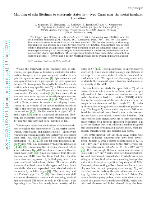
a r X i v :0706.1884v 1 [c o n d -m a t .m t r l -s c i ] 13 J u n 2007APS/123-QEDMapping of spin lifetimes to electronic states in n -type GaAs near the metal-insulatortransitionL.Schreiber,M.Heidkamp,T.Rohleder,B.Beschoten,∗and G.G¨u ntherodtII.Physikalisches Institut,and Virtual Institute for Spin Electronics (ViSel),RWTH Aachen University,Templergraben 55,52056Aachen,Germany(Dated:February 1,2008)The longest spin lifetimes in bulk n -GaAs exceed 100ns for doping concentrations near the metal-insulator transition (J.M.Kikkawa,D.D.Awschalom,Phys.Rev.Lett.80,4313(1998)).The respective electronic states have yet not been identified.We therefore investigate the energy dependence of spin lifetimes in n -GaAs by time-resolved Kerr rotation.Spin lifetimes vary by three orders of magnitude as a function of energy when occupying donor and conduction band states.The longest spin lifetimes (>100ns)are assigned to delocalized donor band states,while conduction band states exhibit shorter spin lifetimes.The occupation of localized donor band states is identified by short spin lifetimes (∼300ps)and a distinct Overhauser shift due to dynamic nuclear polarization.PACS numbers:78.47.+p,78.55.Cr,85.75.-dWithin the framework of the emerging field of spin-tronics,the spin degree of freedom is exploited for infor-mation storage as well as processing and could serve as a qubit for quantum computation [1].Spin coherence and long spin lifetimes are a prerequisite for novel spintronic devices.Electron spins in Si-doped bulk n -GaAs drew at-tention,when long spin lifetimes T ∗2>100ns and coher-ence lengths larger than 100µm were determined using time-resolved Faraday rotation [2,3].Since then n -GaAs was used as a model system to investigate spin injectionand spin transport phenomena [4,5,6].The long T ∗2of bulk n -GaAs,however,is restricted to a doping concen-tration in the vicinity of the metal-insulator transition (MIT)and shortens dramatically towards both sides of the transition [2,7].Similar results in n -type GaN [8],and n -type Si [9]point to a universal phenomenon.How-ever,the respective electronic states yielding these long T ∗2near the MIT have not been identified so far.Various spin relaxation mechanisms have been consid-ered to explain the dependence of T ∗2on carrier concen-tration,temperature,and magnetic field B .The relevant relaxation mechanisms differ substantially for delocalized spins with,e.g.,the D’yakonov-Perel’(DP)dephasing mechanism [10,11,12,13],and for spins localized at im-purity sites with,e.g.,relaxation by hyperfine interaction [13,14,15].Concerning the electronic states of n -type semiconductors,the MIT was shown to occur within the donor band (DB)[16],which is separated from the con-duction band (CB).Near the Fermi level (E F ),the elec-tronic structure is governed by both doping induced dis-order and local Coulomb correlation.The former yields Anderson-localized states in the upper and lower donor band-tails,which are separated from extended states in the center by mobility edges [17].The latter may lead to a Coulomb gap U at E F [18].Both interactions yield a complex electronic structure with coexisting localized and delocalized DB states as well as CB states.Spin dephasing in n -GaAs has mostly been investigated forstates at E F [2,3].There is,however,no energy-resolvedstudy of T ∗2,which would allow to assign spin lifetimes to the respective electronic states of both the donor and the conduction band.We expect that this assignment helps to identify the dominant spin relaxation mechanisms in the vicinity of the MIT.In this Letter,we study the spin lifetime T ∗2of co-herent electron spin states in n -GaAs,which are opti-cally excited in both the donor and conduction band and probed by time-resolved Kerr rotation (TRKR)at 6K.Due to the coexistence of distinct electronic states,thesample is not characterized by a single T ∗2:T ∗2varies by three orders of magnitude as a function of photon en-ergy.The longest T ∗2values which may exceed 100ns are found for delocalized donor band states,while free con-duction band states exhibit shorter spin lifetimes.Our time-resolved Kerr signal shows up to three exponential decay regimes with different precession frequencies.The latter can change due to an additional nuclear magnetic field arising from dynamically polarized nuclei,when res-onantly pumping spins into localized DB states.Two (001)-oriented,500µm thick GaAs wafers with different Si-doping concentrations have been investi-gated:Sample A with a carrier concentration of (2.4±0.2)×1016cm −3is doped close to the MIT (critical car-rier concentration in Si:GaAs n c ∼=1.5×1016cm −3)[16].Reference sample B has a carrier concentration of (1.5±0.4)×1018cm −3and is therefore degenerated [18].We used two tuneable,mode-locked Ti:Al 2O 3lasers pro-viding ∼150fs optical pulses corresponding to a spectral width of ≈6nm at a repetition frequency of 80MHz.Electronic phase-locking of both lasers enables us to em-ploy one laser for spin pumping at an energy E pu and the other one for probing the spin orientation at an en-ergy E pr after a variable delay time ∆t =0...16ns.The normal-incident pump pulses,which were circularly po-larized by a photo-elastic modulator (PEM),excite spin-polarized electrons and holes oriented along the beam2∆t (ps)θ∆t (ps)∆t (ps)sample Bsample A2.00-0.8θK (arb. units)7.60-5.3θK (arb. units)FIG.1:(Color)Time-resolved Kerr rotation for photon en-ergies E =E pu =E pr at 6K with (a)θK (∆t )for sample A at B =1T;the red line shows the shift of the beating node;(b)θK (∆t,E )for sample A at B =1T;(c)θK (∆t,E )for the degenerate sample B at B =6T.Arrows mark the respective energies,above which the transmission drops below 5%.direction in the strain-free mounted samples with an av-erage power P =50W/cm 2.The projection of the pump induced spin magnetization onto the surface nor-mal of the sample is determined with linearly polarized laser pulses by Faraday rotation θF in transmission and by Kerr rotation θK in reflection.Transverse magnetic fields B are applied in the plane of the sample.In Figure 1(a),we plot θK (∆t )of sample A measured for various photon energies E =E pu =E pr at B =1T and at T =6K.Obviously,the spins precess at all energies E ,but the damping of the oscillations andthus T ∗2is E -dependent:for E below the CB edge T ∗2is long,whereas for the highest E ,at which CB states arepumped,T ∗2is much reduced.Strikingly,a node in the oscillation envelope (red line in Fig.1(a))near the band edge indicates that the spins precess with at least two Larmor frequencies ω(i ).Therefore,θK (∆t )is described by n decay componentsθK (∆t )=n iA (i )exp−∆t3 constant and exhibits|g∗|=|g0|=0.43.Near the CBedge(green),B-independent values of T∗2∼100...300psare determined,which distinguish themselves by a rapiddecrease ofω(E).At the beginning of the third region(blue),T∗2sets-in at∼6ns and decreases with increasingE.The correspondingωdecreases slightly and saturatesat high E.The overlap in energy of the second and thirdregion,which occurs due to the spectral width of thelaser pulses,generates the node in the oscillation enve-lope shown in Figure1[19].For the degenerate sample B,T∗(i) 2(E)can befitted by one component i.As expected[2,7],T∗2is over-all shorter compared to sample A and T∗2increases with the increase of B,which is typical for the DP dephasing mechanism[10].In the following,we assign the T∗(i)2of the spins ob-served in the three energy ranges to carriers occupying different electronic states.Since hole spins relax quickly 10ps in GaAs and excitons are broken up at high magneticfields B 1T[20],we consider single elec-tron states.Since the carrier concentration of sample A is slightly above n c,E F lies within the delocalized DB states as sketched in Figure3.Thus delocalized DB states are pumped at lowest E,which exhibit the longest T∗2(red component in Fig.2).However,to our knowl-edge there is no relaxation mechanism of spins,which accounts for their distinct B-dependence.We assign the second energy range(green),which is missing for the degenerate sample B,to Anderson localized electronic states at the DB tail.Their distinct E-dependence of ωand T∗2can be linked to the decrease of localization length upon approaching the DB tail.The localization of electrons yields spin relaxation due to hyperfine inter-action with the nuclei[14,15].This gives rise to dynamic nuclear polarization and a nuclearfield,which altersω(Overhauser shift)[21].However,from Ref.[14]long T∗2∼300ns are expected for localized electron spins, although we could not reproduce this result with insu-lating n-GaAs samples using TRKR.In Ref.[15],an additional short T∗2∼100ps component is predicted, when both localized and delocalized spins are pumped. This is assigned to their cross-relaxation rate.Whereas this might explain our short T∗2,it does not account for the distinctω(E)dependence.In the third energy regime (blue),electrons are pumped in the CB.The decrease of ωobserved for both samples is due to g∗:The absorption of the pump pulse lifts the local chemical potential,thus reducing the absolute value of the energetically averaged g∗factor according to its dispersion in the CB[20].The apparent decrease of T∗2(E)might be explained by car-rier cooling and interband relaxation.Due to both,the carriers relax below the probed energy.This notion can be confirmed by sweeping E pu with E pr heldfixed at the bottom of the CB.The corre-spondingfits of T∗(i)2(E pu)andω(i)(E pu)of sample Aat B=1T are shown in Figure3(a)and(b).Indeed,pr23452345E (eV)E (eV)T(i)2*(ps)T(i)2*(ps)ω(i)/ω0FIG.3:(Color)Upper left:sketch of density of DB and CBstates.Fitted spin lifetimes T∗(i)2and Larmor frequenciesω(i) as a function of pump laser energy E pu at magneticfields B for MIT sample A(full symbols)for different probe energies E pr is marked with vertical grey lines.For comparison data from Fig.2with E pu=E pr are also plotted(open symbols).this method allows to correct T∗2for energy relaxation, since T∗2(E pu)(blue full symbols)decreases only slightly compared to Figure2.However,there is an additionalshort T∗(i)2(E pu)(green full symbols),which results from probing localized spins at the DB tail because of the spec-tral width of the probe pulses.To clarify this point, E pr isfixed at an energy even lower than the band gap(Fig.3(c)-(e)).For this E pr,the longest T∗(i)2(E pu)(red) attributed to delocalized DB states is observed,which turned out to be nearly constant at B=0T.Note that the average pump power is held constant,but the excited carrier density changes by orders of magnitude in the ab-sorbing regime.This has a negligible effect on the longest T∗2.More strikingly,additional components i become ob-servable,when E pu passes the localized and CB states. Thus,different electronic states become occupied either due to direct optical excitation or carrier relaxation as sketched in Figure3(upper left).From the onset of the θF signal(not shown),we deduce that the delocalized DB states are occupied within∆t<10ps for all E pu. At B=1T(Fig.3(d))and E pu beyond the band edge,the two long T∗(i)2components(blue and red)generate nodes in the oscillation envelope(Fig.1(a))and can be separated by theirω(i)(Fig.3(e)).Forfitting,however, the longest T∗2(red)of delocalized DB had to befixed with minor influence on the blue component.The lat-4∆t (ns)FIG.4:(Color)Faraday rotationθF(∆t)of sample A for left(σ−)and right(σ+)circularly polarized pump pulses(red ar-rows)at B=1T,E pu=1.514eV and E pr=1.494eV.Inset:fitted normalized Larmor frequenciesω(i)and correspondinglateral nuclear magneticfields BN for both polarizations as afunction of the average pump power.ter can be clearly assigned to CB states by comparing it to T∗2(E pu)and g∗(E pu)of Figure3(a)and(b).The existence of three components i and their onset whensweeping E pu confirms our assignment of T∗(i)2(E)to thethree types of electronic states.Since an optically pumped spin imbalance of localized electrons leads to pronounced dynamic nuclear polariza-tion(DNP)[21],wefinally check our assignment of elec-tronic states to T∗2by identifying DNP.When resonantly exciting localized spins at,e.g.,E pu=1.514eV,then DNP is optically observed by the Overhauser shift.This shift results in a change ofωdue to the presence of a lateral nuclear magneticfield B N adding up to B.Since spins exhibiting long T∗2are most sensitive to this shift, we chose the same E pr as in Figure3(c)-(e).In order to generate a well-defined longitudinally pumped spin com-ponent and thus to control the direction of B N with re-spect to B,we replaced the PEM by a quarter-waveplate and rotated sample A as sketched in Figure4[22].In this geometry,θF(∆t)exhibits nodes in the oscillation envelope at long∆t,proving the presence of two longT∗(i) 2components with differentω(i).The dependence ofωon the type of circularly polarizationσ±of the pump pulses,is clarified by thefittedω(i)in the inset of Fig-ure4.The sign and magnitude of B N is determined by σ±and the pump power,respectively.B N saturates for σ+at-90mT,when|g∗|=0.43is assumed to be con-stant.However,the blue component,which is likely due to spins in the CB(cp.to Fig.3(e)),is more sensitive to B N than the spins attributed to delocalized DB states (red).However,this point needs further investigation. Since DNP is not observable when E pu is reduced below 1.5eV,our assignment of localized states is confirmed. The pronouncedω(loc)(E)dependence of the localized spins(green)(see Fig.2left)compared to theωvari-ation(blue)in the inset of Figure4suggests that the ω(loc)(E)is indeed influenced by increasing localization and thus responsible for a rise of B N at the DB tail[23]. In summary,we have studied the energy dependence of spin lifetimes in n-type GaAs for electron doping near the metal-insulator transition.Distinct spin lifetimes have been assigned to both donor and conduction band states. Spin states at the Fermi level are delocalized donor band states with the longest spin lifetime,which may exceed 100ns.The strong decrease of spin lifetimes in the con-duction band is related to energy relaxation of hot elec-trons.Localized donor band states exhibit the shortest spin lifetimes of∼300ps.Resonant optical pumping of these localized states yields strong dynamic nuclear po-larization.This work was supported by BMBF and by HGF.∗Electronic address:beschoten@physik.rwth-aachen.de [1]D.D.Awschalom and M.E.Flatte,Nature Phys.3,153(2007).[2]J.M.Kikkawa and D.D.Awschalom,Phys.Rev.Lett.80,4313(1998).[3]J.M.Kikkawa and D.D.Awschalom,Nature397,139(1999).[4]Y.Kato et al.,Science306,1910(2004).[5]S.A.Crooker et al.,Science309,2191(2005).[6]X.Lou et al.,Nature Phys.3,197(2007).[7]R.I.Dzhioev et al.,Phys.Rev.B66,245204(2002).[8]B.Beschoten et al.,Phys.Rev.B63,121202R(2001).[9]V.Zarifis and T.G.Castner,Phys.Rev.B36,6198(1987).[10]J.Fabian and S.D.Sarma,J.Vac.Sci.Technol.B17,1708(1999).[11]P.H.Song and K.W.Kim,Phys.Rev.B66,035207(2002).[12]Z.G.Yu et al.,Phys.Rev.B71,245312(2005).[13]B.I.Shklovskii,Phys.Rev.B73,193201(2006).[14]R.I.Dzhioev et al.,JETP Lett.74,200(2001).[15]W.O.Putikka and R.Joynt,Phys.Rev.B70,113201(2004).[16]D.Romero et al.,Phys.Rev.B42,3179(1990).[17]P.Anderson,Phys.Rev.189,1492(1958).[18]A.Efros and M.Pollak,eds.,Electron-Electron Interac-tion in Disordered Systems(North-Holland,Amsterdam, 1984).[19]The third region sets in at even lower energy E≈1.514eV,where T∗2cannot be determined exactly dueto the beating.[20]M.Oestreich et al.,Phys.Rev.B53,7911(1996).[21]D.Paget et al.,Phys.Rev.B15,5780(1977).[22]G.Salis et al.,Phys.Rev.B64,195304(2001).[23]Even with the PEM,ωchanges whithin∼1min afterswitching on the pump.We attribute this to an Over-hauser shift.。
Oscillating magnetoresistance in diluted magnetic semiconductor barrier structures
Kai Chang∗ and J. B. Xia
NLSM, Institute of Semiconductors, Chinese Academy of Sciences, Beijing 100083, China
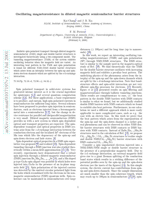
distances (≥ 100µm) and for long time (up to nanoseconds) [16]. In this work, we report an interesting oscillating tunneling magnetoresistance (TMR) and spin polarization (SP) through NMS/DMS structures. The DMS structure is similar to the saal study of Ref. [10]. We find theoretically that the TMR for the double barrier structure oscillates with increasing magnetic field and exhibits a peculiar beat pattern. The underlying physics of the phenomena arises from the interplay of the spin-up and the spin-down channels which are split by the s-d exchange interaction. Note that bandstructure effects and spin-orbit interaction are not very efficient spin-flip processes for electrons. [17] Recently, Egues et al [12] presented results on spin filtering and magnetoresistance through ballistic tunneling junctions. These results are complementary to ours, i.e. the beat pattern in the double NMS barriers with DMS contacts is similar to what we found, but we additionally studied double DMS barriers with NMS contacts which we found to exchibit also beat patterns. Furthermore, in our calculation we used a different approach which is more easily applicable to more complicated cases, such as e.g. the case with an electric bias. In this work we prove that the beat pattern which arises from the superposition of the spin-up and the spin-down channel is a rather general phenomena and can be observed in either NMS double barrier structures with DMS contacts or DMS barriers with NMS contacts. Instead of ZnSe/Zn1−x Mnx Se structures used in the calculation of Ref. [12], we propose Cd1−y Mgy Te / Cd1−x Mnx Te structures to realize single and double NMS(Cd1−y Mgy Te) barrier structures with DMS contacts(Cd1−x Mnx Te). Consider a spin unpolarized electron injected into a NSM/DMS/NSM single or double barrier structure in the presence of a perpendicular magnetic field. Due to the s-d exchange interaction, an external magnetic field gives rise to a giant Zeeman splitting of the conduction band states which results in a striking difference of the potential profiles seen by the spin-up and the spin-down electron (see the insets of the figures) [11]. In this simple system, the electric current has contributions from spinup and spin-down channels. Since the sample dimensions are much smaller than the spin coherence length, which may reach up to 100µm in semiconductors [14,16], spin-
Temperature Dependence of the Spin Polarization of a Quantum Hall Ferromagnet
1
A rapidly growing body of evidence, both theoretical [1{3] and experimental [4{7], strongly suggests that the lowest-lying charged excitation of the spin-polarized = 1 quantum Hall state is a spin-texture called a Skyrmion. This many-body state consists of radial spin density that is reversed at the center but gradually heals to the spin background over many magnetic lengths. The spin density distribution is determined by the interplay of the ferromagnetic exchange interaction and the Zeeman energy. The exchange interaction favors large Skyrmions while the Zeeman term favors smaller excitations. In GaAs samples presently under investigation the exchange energy can be up to two orders of magnitude larger than the Zeeman energy. Hartree-Fock calculations [2] predict that Skyrmions should consist of 3 4 spin ips per unpaired ux quantum for small excursions about = 1, a result consistent with early experimental work on the lling factor ( ) dependence of the zero temperature spin polarization near = 1 [4,6]. This dominance of the exchange interaction over the Zeeman energy has led theorists to refer to the = 1 quantum Hall state as the quantum Hall ferromagnet. In GaAs heterostructures experimentalists are presented an unprecedented opportunity to probe the physics of two-dimensional electron ferromagnetism in a well-characterized system. Thus insights gained from the thermodynamics of the spin polarization will be of interest not only to those studying many-body e ects in the integral quantum Hall regime, but also more generally, may elucidate the physics of 2D electron magnetism. In this communication we report on the experimental determination of the spin polarization as a function of temperature for such a = 1 quantum Hall ferromagnet. The system consists of a single-side n-modulation doped AlGaAs-GaAs single quantum well (SQW). The well thickness is 250 with an electron density of Ns = 1:8 10 cm and mobilA ity = 2:6 10 cm =V s. In order to perform absorption measurements the samples were mounted strain-free and thinned to 0:5m. The spin polarization is monitored through band-to-band absorption spectroscopy which distinguishes the occupancy of the two electron spin states. Band-gap absorption spectra show striking temperature dependence due to changes in the occupations of the spin-split states of the ground Landau level at lling factors
- 1、下载文档前请自行甄别文档内容的完整性,平台不提供额外的编辑、内容补充、找答案等附加服务。
- 2、"仅部分预览"的文档,不可在线预览部分如存在完整性等问题,可反馈申请退款(可完整预览的文档不适用该条件!)。
- 3、如文档侵犯您的权益,请联系客服反馈,我们会尽快为您处理(人工客服工作时间:9:00-18:30)。
Gated Spin Transport through an Individual SingleWall Carbon NanotubeBhaskar Nagabhirava,1Tanesh Bansal, Gamini Sumanasekera,2Lei Liu,3and Bruce W. Alphenaar1* 1Department of Electrical and Computer Engineering, University of Louisville, Louisville, KY, 40292 2Department of Physics, University of Louisville, Louisville, KY, 40292 3Department of Physics, McGill University, Montreal, Quebec, Canada, H3A 2T8*Corresponding Author: Phone: 502-852-1554; Fax: 502-852-1577; Email: brucea@ABSTRACT Hysteretic switching in the magnetoresistance of short-channel, ferromagnetically contacted individual single wall carbon nanotubes is observed, providing strong evidence for nanotube spin transport. By varying the voltage on a capacitively coupled gate, the magnetoresistance can be reproducibly modified between +10% and -15%. The results are explained in terms of wave vector matching of the spin polarized electron states at the ferromagnetic / nanotube interfaces.Due to their unique structural and electrical properties, carbon nanotubes have been investigated extensively for possible electronic device applications.1 Carbon nanotube spin electronics, while less thoroughly explored, also holds substantial promise.2 Carbon nanotubes have large electron scattering lengths (measured to be 10 microns or higher at room temperature)3 and weak spin orbit coupling, so that the nanotube spin scattering length is expected to be extremely large. Initial evidence for spin transport through nanotubes was provided by the observation of hysteretic magnetoresistance switching in ferromagnetically contacted multi wall nanotubes (MWNTs).4 These results have since been reproduced and expanded on by a number of authors.5,6There have also been numerous attempts to observe evidence for spin transport through ferromagnetically contacted single wall nanotubes (SWNTs).2, 7-10 SWNTs offer many advantages over MWNTs for spin transport studies, including increased scattering lengths, well-defined electronic band structure, enhanced Coulombic interactions (leading to novel physical phenomena), and the possibility to modify the nanotube resistance with a capacitively coupled gate. A less obvious advantage of the SWNT is that the SWNT resistance shows a much weaker dependence on magnetic field than the MWNT.11 The large intrinsic MWNT magnetoresistance in combination with the fringing field from the ferromagnetic contacts can produce resistance changes that mimic those due to spin transport.2 Despite these advantages, measurements of SWNTs have so far provided less than ideal evidence for spin transport. Some groups have reported magnetoresistance switching in ferromagnetically contacted SWNTs,2,7,8 while others fail to observe even a background magnetoresistance.9 Four-terminal measurements of SWNTs provide evidence that some fraction of the observed magnetoresistance is due to spin transport through the nanotubes.10 However, magnetoresistance switching has recently been reported in SWNT devices having only one semiconducting ferromagnetic contact, which brings into question the validity of interpreting any of the magnetoresistance data in terms of spin transport.8There is no clear answer for why it has been so difficult to demonstrate SWNT spin transport in a reliable manner. One possibility though, is that the nanotube transport length must be made much shorter than simple scattering considerations would imply in order for spin mediated resistance changes to be observed consistently. Experiments suggest that at low temperatures, carbon nanotubes can behave as one or a series of conducting islands (rather than as a ballistic wire).12 Transport through such small islands will be dominated by Coulomb charging effects, which will greatly increase the electron transport time, and consequently provide more time for spin scattering to occur.13 Another factor that has not been fully appreciated is the influence of Lüttinger liquid phenomena,14 which could provide additional pathways for spin scattering that are not available in a Fermi liquid. Irrespective of the exact spin scattering mechanism, it is reasonable to assume that reduction of the nanotube transport length should improve the chance of observing spin transport. Once reliably observed, it will then be possible to characterize the spin scattering mechanisms and optimize the spin mediated resistance signal.We have fabricated and characterized ferromagnetically contacted “short channel” SWNT devices that show clear hysteretic switching in the magnetoresistance, and provide strong evidence for SWNT spin transport. The main difference between our work and previous studies is that we have greatly reduced the transport length separating the ferromagnetic contacts to distances on the order of 10 nm. Preliminary measurements demonstrate this reduction to be extremely beneficial. We have observed clear hysteretic switching in the magnetoresistance in 75% of our devices, and are able to modify the magnetoresistance between +15% and -10% as a function of gate voltage. The gate mediated change in magnitude and sign of the magnetoresistance switching allows us to discount other non-spin related sources for the observed signal and provides the basis for the first SWNT spin transistor.Our fabrication procedure is outlined in Fig. 1. A grid of high-resolution alignment marks is defined on the surface of an oxidized silicon wafer using e-beam lithography and wet etching. The wafer is thendipped into an iron(III)nitride catalyst solution, and single wall nanotubes are grown on the catalyzed surface by placing the wafer in a CH4 atmosphere at 910o C for 3 minutes. This produces well-separated individual SWNTs that are 1-2 nm in diameter, and approximately 15 microns long. After growth, the SWNTs are mapped out with respect to the alignment grid using an atomic force microscope. A two-step process is then performed to define the nanotube contacts. First, the left contact is defined using standard e-beam lithography and e-beam evaporation (Fig. 1(a)). Next, the right contact is defined in a similar fashion, however, during the evaporation step, the sample is angled so that the line of sight to the right contact is partially shadowed by the left contact (Fig. 1(b)). Using this procedure, the contact separation can be made arbitrarily small, simply by varying the deposition angle. Figure 1(c) shows an SEM image of a finished device, having nickel contacts. The contact separation distance is approximately 10 nm. For three-terminal operation, the ferromagnetic contacts form the device source and drain, while the silicon substrate (which is heavily doped) acts as the gate terminal.Fig 2(a) shows the two-terminal magnetoresistance of the device shown in Fig. 1(c), measured at 4.2 K, and with zero voltage on the gate. Measurements were made using a standard lock-in detection scheme using a 100 µV excitation voltage with magnetic field from a superconducting magnet directed parallel to the contacts, and perpendicular to the current flow. (The existence of an appreciable conductance at cryogenic temperatures indicates that this is a metallic nanotube.) As would be expected for spin transport through the nanotube, the resistance is high near zero field when the ferromagnetic moments in the two contacts are anti-parallel, and low when the ferromagnetic moments are parallel.15The percent change in resistance ∆R/R=2Ra −Rp()/R a+R p() is approximately 10%, where R a and R p are the resistances in the anti-parallel and parallel configurations, respectively. Results from other similar devices demonstrate that the short-channel contacting scheme produces a greatly improved yield compared with the standard fabrication technique. Three out of a batch of four devices that were measurable at low temperature showed substantial change in the resistance as a function of magnetic field at 4.2 K (see Figs 2(b) and (c)). By comparison, only one out of more than 100 devices that wemeasured having contact separations of 100 nm or more showed any sign of magnetoresistance switching. (Recently published work on Fe contacted SWNT devices reports a yield of 4 out of 30 for long channel devices.)8Surprisingly, the magnetoresistance trace in Fig. 2 (c) shows that the resistance is minimized in the anti-parallel configuration (near zero field) and maximized in the parallel configuration (above 100 mT) opposite to the predictions of the simple Julliere model.15 All three of the measurements in Fig. 2 were performed with zero bias on the gate. Further measurements show that the gate bias can be used to alter the behavior of the device magnetoresistance between the standard switching (Ra > Rp) and anomalous switching (Rp > Ra) states. Figure 3(a)-(c) shows the magnetoresistance ratio of the device in Fig 2 (b) as a function of magnetic field directed parallel to the contacts for three different values of the gate bias. ∆R/R is clearly dependent on gate bias, varying from approximately +10% to -6% as the bias changes from 1.44 to 2.76 V. In addition, as shown in Fig. 3(b), at certain values of gate bias, very little magnetoresistance is observed. To further elucidate this behavior, we performed a set of similar magnetoresistance measurements on this device at 250 equally spaced values of gate bias between -3V and 11V. The results of these measurements are compiled in Fig. 4, where ∆R/R is plotted as a function of gate bias for (a) negative and (b) positive sweep directions. While somewhat noisy, a series of reproducible fluctuations can clearly be observed. Regimes are observed in which ∆R/R is positive, negative, or close to zero.Because the contact separation is so small, it is important to estimate the magnitude of the current due to leakage via tunneling through the oxide separating the two contacts. Figure 4(c) shows the conductance of the nanotube device as a function of bias on the silicon substrate at B = 100 mT, where the contact magnetizations are in the aligned, or parallel configuration. (These data points were extracted from the same 250 magnetoresistance measurements summarized in Figs. 4(a) and (b).) The conductance is observed to fluctuate by approximately 800% as a function of gate bias. Thesefluctuations are most likely due to the combined influence of Coulomb charging and quantum coherence on the transmission through the nanotube. Our results demonstrate that the primary contribution to the conductance is transport through the nanotube and not leakage, since the leakage current should be independent of gate voltage. The maximum possible conductance due to leakage is equal to the minimum device conductance or approximately 5 x 10⁻⁸ mhos (corresponding to a resistance of 2 x 10⁷Ω). A simple circuit analysis shows that this amount of leakage is insufficient to account for the magnitude of the observed magnetoresistance switching, and is clearly unable to explain the change in sign in the magnetoresistance as a function of gate voltage.Since characterization of the short-channel device requires two-terminal measurements, we must also consider the influence that fringing fields from the ferromagnetic contacts have on the intrinsic SWNT magnetoresistance. For two important reasons, however, we feel that this effect is not a significant source of magnetoresistance in our measurements. First, recent results have shown that, in contrast with MWNTs, the magnetoresistance of SWNTs is very small, and amounts to less than 1% at a field of 1 T at 4.2K.11 This is confirmed by our own measurements, which show no appreciable magnetoresistance beyond the switching that we observe at low fields. Second, this effect does not explain the dramatic improvement in yield that we have achieved simply by decreasing the contact separation. Fringing field effects should be equally important at large and small contact separations. For similar reasons, we feel that our results cannot be related to the magnetoresistance switching recently observed in SWNTs with single ferromagnetic semiconducting contacts.8 Any single contact effect (whose origin is yet to be explained) should be observed equally for large and small contact separations.We can qualitatively understand the mechanism behind the gate dependent magnetoresistance in terms of a simple one-dimensional model that takes into account wave function matching across the ferromagnetic / nanotube / ferromagnetic junction, with different Fermi wave vectors for the spin-up and spin-down electrons in the ferromagnetic regions16 and a variable Fermi wave vector of thenanotube tuned by gate voltage.17 Similar models have previously been applied to magnetic tunnel junctions18 and to MWNTs.6The electron transmission through the junction for the parallel (T p) and antiparallel (T a) configurations is calculated by solving the one-dimensional Schrodinger equation.The resistance ratio is then approximated by R /R = 2(T p-T a)/(T a+T p). Because of the different dispersion and different Fermi wave vectors for the two spin states and the difference of the Fermi wave vectors in the ferromagnetic regions and nanotube region, the outcome of the matching, and hence the transmission coefficient depends on both the magnetic configuration and gate bias. As the gate bias increases, the transmission coefficients T a and T p oscillate, each out of phase from one another, causing oscillation of R /R, as shown in the figure. A more precise description will most likely require treating the nanotube as a quantum dot, and include the influence of Coulomb charging and the zero dimensional electron energy spectrum.19 However, the simple model does indicate that oscillations in the magnitude and sign of the magnetoresistance are expected provided that the nanotube wave vector can be adjusted independently of the contacts.In summary, we have fabricated and characterized ferromagnetically contacted SWNT devices with extremely short contact separation distances. The short-channel allows for the observation of magnetoresistance switching whose gate dependence provides strong evidence for spin transport through the SWNT. We note that the short channel contacting scheme is generally applicable to non-ferromagnetic contacts as well, and provides a straightforward technique for fabricating SWNT quantum dot devices.ACKNOWLEDGMENT The authors thank R.W. Cohn, Q. Si and J. Kono for valuable discussions. Funding provided by ONR / NSF (No. ECS-0224114) and NASA (No. NCC 5-571).REFERENCES(1)Dresselhaus, M.; Dresselhaus, G.; Avouris, P. (Eds.), Carbon Nanotubes: Synthesis, Structure,Properties and Applications, Springer: Berlin, 2001.(2)Alphenaar, B.W.; Chakraborty, S.; Tsukagoshi, K. In Electron Transport in Quantum Dots;Bird, J.P., Ed.; Kluwer Academic / Plenum Publishers; New York, 2003; pp. 433-456.(3)Bachtold, A.; Fuhrer, M.S.; Plyasunov, S.; Forero, M.; Anderson, E.H.; Zettl, A.; McEuen, P.L.Phys. Rev. Lett.2000, 84, 6082; Yao, Z.; Kane, C.L.; Dekker, C. Phys. Rev. Lett.2000, 84, 2941.(4)Tsukagoshi, K.; Alphenaar, B.W.; Ago, H. Nature1999, 401, 572.(5)Orgassa, D.; Mankey, G.J.; Fujiwara, H. Nanotechnology2001, 12, 281; Alphenaar, B.W.;Tsukagoshi, K.; Wagner, M. J. Appl. Phys.2001, 89, 6863; Zhao, B.; Monch, I.; Muhl, T.;Vinzelberg, H.; Schneider, T.M. J. Appl. Phys.2002, 91, 7026; Sahoo, S.; Kontos, T.;Schonenberger, C.; Surgers, C. Appl. Phys. Lett.2005, 86, 112109.(6)Chakraborty, S.; Walsh, K.; Alphenaar, B.W.; Liu, L.; Tsukagoshi, K. Appl. Phys. Lett.2003,83, 1008.(7)Kim, J.R.; So, H.M.; Kim, J.J.; Kim, J. Phys. Rev. B2002, 66, 233401.(8)Jensen, J.; Hauptmann, J.R.; Nygard, J.; Lindelof, P.E. Phys. Rev. B 2005, 72, 035419.(9)Chen, Y.F.; Fuhrer, M.S.; Chung, S.H.; Gomez, R.D. Bulletin of the American Physical Society,2003, 48, 1009.(10)Tombros, N.; van der Molen, S.J.; van Wees, B.J. Preprint, cond-mat/ 0506538.(11)Sagnes, M.; Raquet, B.; Lassagne, B.; Broto, J.M.; Flahaut, E.; Laurent, C.; Ondarcuhu, T.;Carcenac, F.; Vieu, C. Chem. Phys. Lett.2003, 372, 733.(12)Bockrath, M.; Cobden, D.H.; McEuen, P.L.; Chopra, N.G.; Zettl, A.; Thess, A; Smalley, R.E.Science1997, 275, 1922.(13)Brataas A.; Wang, X.H. Phys. Rev. B2001, 64, 104434.(14)Kane, C.; Balents, L.; Fischer, M.P.A. Phys. Rev. Lett.1997, 79, 5086; Egger R.; Gogolin, A.O.;Phys. Rev. Lett.1997, 79, 5082; Balents, L.; Egger, R. Phys. Rev. Lett.2000, 85, 3464.(15)Julliere, M. Phys. Lett.1975, 54A, 225.(16)Stearns, M.B. J. Magn. Magn. Mater.1977, 5, 167.(17)Lemay, S.G.; Janssen, J.W.; van den Hout, M.; Mooij, M.; Bronikowski, M.J.; Willis, P.A.;Smalley, R.E.; Kouwenhoven , L.P.; Dekker, C. Nature2001, 412, 617.(18)Slonczewski, J.C.; Phys. Rev. B 1989, 39, 6995; Moodera, J.S.; Nowak, J.; Kinder, L.R.;Tedrow, P.M. Phys. Rev. Lett. 1999, 83, 3029.(19)Kirchner, S.; Zhu, L.; Si, Q.; Natelson, D. Preprint, cond-mat/0507215.SYNOPSIS TOC (Word Style “SN_Synopsis_TOC”). If you are submitting your paper to a journal that requires a synopsis graphic and/or synopsis paragraph, see the Guide, Notes, Notice, or Instructions for Authors that appear in each publication’s first issue of the year and the journal’s homepage for a description of what needs to be provided and for the size requirements of the artwork.Figure 1. Fabrication of a short-channel nanotube device: (a) Deposition of the left ferromagnetic contact is performed first followed by, (b) deposition of the right ferromagnetic contact. The sample is angled so that the deposition of the right contact is partially shadowed by the left contact. (c) Field emission SEM image of a finished device. The inset shows a close-up of the contact separation, which is approximately 10 nm.Figure 2. Percent change in resistance as a function of magnetic field for three nickel contacted short-channel SWNT devices. The solid (dashed) line corresponds to the positive (negative) sweep direction.Measurements were made at 4.2K with the gate grounded.Figure 3. Magnetoresistance ratio of a nickel contacted, gated, short-channel SWNT device for three different values of the gate bias. The solid (dashed) line corresponds to the positive (negative) sweepdirection. Measurements were made at 4.2KFigure 4. Magnetoresistance ratio of the device in Fig. 3 as a function of gate bias in the (a) forward and (b) reverse sweep directions. (c) Two-terminal conductance of the same device as a function of gatebias. All measurements are at 4.2 K.Figure 5. (a) Parallel and anti-parallel transmission coefficients and (b) the resistance ratio as a function of the gate voltage calculated using a one-dimensional model for a ferromagnetically contacted armchair nanotube. In the nickel contacts, the energy splitting between the spin-up and spin-down electrons E = 1.0 eV, the Fermi energy F E = 2.2 eV and the effective mass m * = 1m e . For the nanotube, the length L=10 nm, m * = 1m e , and k = k 0 + k with k 0 = 0.8509/Å, k=E/F hv , and s m v F /102.85×=. Here E = g eV α with the gate efficiency factor α being taken to be 0.025.。