MAX3221IPWR中文资料
MAXIM MAX3221 MAX3223 MAX3243 说明书

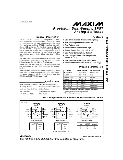
_______________General DescriptionThe MAX3221/MAX3223/MAX3243 achieve 1µA supply current with Maxim’s revolutionary AutoShutdown™ fea-ture. When the MAX3221/MAX3223/MAX3243 do not sense a valid signal level on their receiver inputs, the on-board power supply and drivers shut down. This occurs if the RS-232 cable is disconnected or if the transmitters of the connected peripheral are turned off.The system turns on again when a valid level is applied to any RS-232 receiver input. As a result, the system saves power without changes to the existing BIOS or operating system.The MAX3221/MAX3223/MAX3243 transceivers are 3V-powered EIA/TIA-232 and V.28/V.24 communications interfaces intended for notebook computer applica-tions. A proprietary, high-efficiency, dual charge-pump power supply and a low-dropout transmitter combine to deliver true RS-232 performance from a single +3.0V to +5.5V supply. A guaranteed data rate of 120kbps pro-vides compatibility with popular software for communi-cating with personal computers.The MAX3221/MAX3223/MAX3243 require only 0.1µF capacitors in 3.3V operation, and can operate from input voltages ranging from +3.0V to +5.5V. They are ideal for 3.3V-only systems, mixed 3.3V and 5.0V systems, or 5.0V-only systems that require true RS-232 performance.The MAX3221 is a 1-driver/1-receiver 16-pin SSOP ver-sion of the 20-pin MAX3223 (2-driver/2-receiver). The MAX3243 3-driver/5-receiver, complete serial port is ideal for notebook or subnotebook computers. The MAX3243 includes one complementary always-active receiver. This receiver can monitor an external device (such as a modem) in shutdown, without forward bias-ing the protection diodes in a UART that may have V CC completely removed.Next Generation Device Features♦For Space-Constrained Applications:MAX3228/MAX3229: +2.5V to +5.5V RS-232Transceivers in UCSP™♦For Integrated ESD Protection:MAX3222E/MAX3232E/MAX3237E/MAX3241E*/MAX3246E: ±15kV ESD-Protected, Down to 10nA,3.0V to 5.5V, Up to 1Mbps, True RS-232Transceivers (MAX3246E Available in UCSP Package)♦For Low-Voltage or Data Cable Applications:MAX3380E/MAX3381E: +2.5V to +5.5V, 1µA, 2 Tx/2 Rx RS-232 Transceivers with ±15kV ESD-Protected I/O and Logic Pins________________________ApplicationsNotebook, Subnotebook, and Palmtop Computers Battery-Powered Equipment Hand-Held Equipment Peripherals PrintersMAX3221/MAX3223/MAX3243*1µA Supply-Current, True +3V to +5.5V RS-232 Transceivers with AutoShutdown________________________________________________________________Maxim Integrated Products119-0306; Rev 8; 10/03* Covered by U.S. Patent numbers 4,636,930; 4,679,134; 4,777,577; 4,797,899; 4,809,152; 4,897,774; 4,999,761; and other patents pending.†Future product—contact factory for availability.AutoShutdown and UCSP are trademarks of Maxim Integrated Products, Inc.Pin Configurations appear at end of data sheet.Typical Operating Circuits appear at end of data sheet._____________________Selector GuideFor pricing, delivery, and ordering information,please contact Maxim/Dallas Direct!at 1-888-629-4642, or visit Maxim’s website at .M A X 3221/M A X 3223/M A X 32431µA Supply-Current, True +3V to +5.5V RS-232 Transceivers with AutoShutdown 2_______________________________________________________________________________________ABSOLUTE MAXIMUM RATINGSELECTRICAL CHARACTERISTICS(V CC = +3.0V to +5.5V, C1–C4 = 0.1µF (Note 2), T A = T MIN to T MAX , unless otherwise noted. Typical values are at T A = +25°C.)Stresses beyond those listed under “Absolute Maximum Ratings” may cause permanent damage to the device. These are stress ratings only, and functional operation of the device at these or any other conditions beyond those indicated in the operational sections of the specifications is not implied. Exposure to absolute maximum rating conditions for extended periods may affect device reliability.V CC ...........................................................................-0.3V to +6V V+ (Note 1)...............................................................-0.3V to +7V V- (Note 1)...............................................................+0.3V to -7V V+ + |V-|(Note 1).................................................................+13V Input VoltagesT_IN, FORCEOFF , FORCEON, EN (MAX3223)......-0.3V to +6V R_IN...................................................................................±25V Output VoltagesT_OUT.............................................................................±13.2V R_OUT, INVALID ......................................-0.3V to (V CC + 0.3V)Short-Circuit DurationT_OUT......................................................................Continuous Continuous Power Dissipation (T A = +70°C)16-Pin SSOP (derate 7.14mW/°C above +70°C)...........571mW 16-Pin TSSOP (derate 6.70mW/°C above +70°C).........533mW 20-Pin Plastic DIP (derate 11.11mW/°C above +70°C)....889mW 20-Pin SSOP (derate 8.00mW/°C above +70°C)...........640mW 20-Pin TSSOP DIP (derate 7.00mW/°C above +70°C).....559mW 28-Pin Wide SO (derate 12.50mW/°C above +70°C)............1W 28-Pin SSOP (derate 9.52mW/°C above +70°C)...........762mW 28-Pin TSSOP (derate 8.70mW/°C above +70°C).........696mW Operating Temperature RangesMAX32_ _C_ _.......................................................0°C to +70°C MAX32_ _E_ _....................................................-40°C to +85°C Storage Temperature Range.............................-65°C to +150°C Lead Temperature (soldering, 10s).................................+300°CNote 1:V+ and V- can have maximum magnitudes of 7V, but their absolute difference cannot exceed 13V.1µA Supply-Current, True +3V to +5.5V RS-232 Transceivers with AutoShutdown_______________________________________________________________________________________3ELECTRICAL CHARACTERISTICS (continued)(V CC = +3.0V to +5.5V, C1–C4 = 0.1µF (Note 2), T A = T MIN to T MAX , unless otherwise noted. Typical values are at T A = +25°C.)Note 2:C1–C4 = 0.1µF, tested at 3.3V ±10%. C1 = 0.047µF, C2–C4 = 0.33µF, tested at 5.0V ±10%.M A X 3221/M A X 3223/M A X 32431µA Supply-Current, True +3V to +5.5V RS-232 Transceivers with AutoShutdown 4_________________________________________________________________________________________________________________________________Typical Operating Characteristics(V CC = +3.3V, 235kbps data rate, 0.1µF capacitors, all transmitters loaded with 3k Ω, T A = +25°C, unless otherwise noted.)-6-5-4-3-2-101234560MAX3221/MAX3223TRANSMITTER OUTPUT VOLTAGEvs. LOAD CAPACITANCELOAD CAPACITANCE (pF)T R A N S M I T T E R O U T P U T V O L T A G E (V )20003000100040005000246810121416182022150500MAX3221/MAX3223SLEW RATEvs. LOAD CAPACITANCELOAD CAPACITANCE (pF)S L E W R A T E (V /µs )2000300010004000500051015202530354005101520253035MAX3221/MAX3223SUPPLY CURRENT vs. LOAD CAPACITANCEWHEN TRANSMITTING DATALOAD CAPACITANCE (pF)M A X 3223 S U P P L Y C U R R E N T (m A )M A X 3221 S U P P L Y C U R R E N T (m A )20003000100040005000-7.5-5.0-2.502.55.07.50MAX3243TRANSMITTER OUTPUT VOLTAGEvs. LOAD CAPACITANCELOAD CAPACITANCE (pF)T R A N S M I T T E R O U T P U T V O L T A G E (V )2000300010004000500046810121416182022240MAX3243SLEW RATEvs. LOAD CAPACITANCELOAD CAPACITANCE (pF)S L E W R A T E (V /µs )20003000100040005000510152025303545400MAX3243SUPPLY CURRENT vs. LOADCAPACITANCE WHEN TRANSMITTING DATALOAD CAPACITANCE (pF)S U P P L Y C U R R E N T (m A )20003000100040005000MAX3221/MAX3223/MAX32431µA Supply-Current, True +3V to +5.5V RS-232 Transceivers with AutoShutdown_______________________________________________________________________________________5______________________________________________________________Pin DescriptionLapLink is a trademark of Traveling Software._______________Detailed DescriptionDual Charge-Pump Voltage ConverterThe MAX3221/MAX3223/MAX3243’s internal power supply consists of a regulated dual charge pump that provides output voltages of +5.5V (doubling charge pump) and -5.5V (inverting charge pump), regardless of the input voltage (V CC ) over the +3.0V to +5.5V range. The charge pumps operate in a discontinuous mode: if the output voltages are less than 5.5V, the charge pumps are enabled; if the output voltages exceed 5.5V, the charge pumps are disabled. Each charge pump requires a flying capacitor (C1, C2) and a reservoir capacitor (C3, C4) to generate the V+ and V- supplies.RS-232 TransmittersThe transmitters are inverting level translators that con-vert CMOS-logic levels to 5.0V EIA/TIA-232 levels. They guarantee a 120kbps data rate with worst-case loads of 3k Ωin parallel with 1000pF, providing compatibility with PC-to-PC communication software (such as Laplink™).Typically, the MAX3221/MAX3223/MAX3243 can oper-ate at data rates of 235kbps. Transmitters can be paral-leled to drive multiple receivers or mice (MAX3243).Figure 1 shows a complete system connection.When FORCEOFF is driven to ground, or the Auto-Shutdown circuitry senses invalid voltage levels at all receiver inputs, the transmitters are disabled and the outputs are forced into a high-impedance state.M A X 3221/M A X 3223/M A X 32431µA Supply-Current, True +3V to +5.5V RS-232 Transceivers with AutoShutdown 6_______________________________________________________________________________________RS-232 ReceiversThe MAX3221/MAX3223/MAX3243’s receivers convert RS-232 signals to CMOS-logic output levels. All receivers have one inverting three-state output. In shut-down (FORCEOFF = low) or in AutoShutdown, the MAX3221/MAX3223’s receivers are active (Table 1).Driving EN high places the receiver(s) in a high-imped-ance state. The MAX3243’s receivers are high imped-ance when the part is shut down.The MAX3243 has an always-active complementary output (R2OUTB). R2OUTB is an extra output that mon-itors receiver activity while the other receivers are high impedance. This allows Ring Indicator to be monitored without forward biasing other devices connected to the receiver outputs. This is ideal for systems where V CC is set to 0V in shutdown to accommodate peripherals,such as UARTs (Figure 2).Figure 1. Interface Under Control of PMUFigure 2. The MAX3243 detects RS-232 activity when the UART and interface are shut down.MAX3221/MAX3223/MAX32431µA Supply-Current, True +3V to +5.5V RS-232 Transceivers with AutoShutdown_______________________________________________________________________________________7AutoShutdownA 1µA supply current is achieved with Maxim’s new AutoShutdown feature, which operates when FORCEON is low and FORCEOFF is high. When the MAX3221/MAX3223/MAX3243 sense no valid signal levels on all receiver inputs for 30µs, the on-board power supply and drivers are shut off, reducing supply current to 1µA. This occurs if the RS-232 cable is dis-connected or the connected peripheral transmitters are turned off. The system turns on again when a valid level is applied to any RS-232 receiver input. As a result, the system saves power without changes to the existing BIOS or operating system. When using AutoShutdown,the INVALID output is high when the device is on and low when the device is shut down. Because I NVALID indicates the receiver inputs’ condition, it can be used in any mode (Figure 3).Table 2 and Figure 3c summarize the MAX3221/MAX3223/MAX3243operating modes. FORCEON and FORCEOFF override the automatic circuitry and force the transceiver into its normal operating state or into its low-power standby state. When neither control is assert-ed, the IC selects between these states automatically based on receiver input levels. Figures 3a, 3b, and 5a depict valid and invalid RS-232 receiver levels.A mouse or other system with AutoShutdown may need time to wake up. Figure 4 shows a circuit that forces the transmitters on for 100ms, allowing enough time for theFigure 3a. MAX32_ _ Entering 1µA Supply Mode via AutoShutdown*Note:If the part is in AutoShutdown mode (FORCEOFF = V CC ,FORCEON = GND), it is shut down if no valid RS-232levels are present on all receiver inputs.Figure 4. AutoShutdown with Initial Turn-On to Wake Up a Mouse or Another SystemM A X 3221/M A X 3223/M A X 32431µA Supply-Current, True +3V to +5.5V RS-232 Transceivers with AutoShutdown 8_______________________________________________________________________________________other system to realize that the MAX3221/MAX3223/MAX3243is awake. If the other system outputs valid RS-232 signals within that time, the RS-232 ports on both systems remain enabled.When shut down, the device’s charge pumps are turned off, V+ decays to V CC , V- decays to ground, and the transmitter outputs are disabled (high impedance). The time required to exit shutdown is typically 100µs (Figure 5b).Software-Controlled ShutdownIf direct software control is desired, INVALID can be used to indicate DTR or Ring Indicator signal. Tie FORCEOFF and FORCEON together to bypass Auto-Shutdown so the line acts like a SHDN input.___________Applications InformationCapacitor SelectionThe capacitor type used for C1–C4 is not critical for proper operation; either polarized or nonpolarized capacitors may be used. The charge pump requires 0.1µF capacitors for 3.3V operation. For other supply voltages, refer to Table 3 for required capacitor values.Do not use values smaller than those listed in Table 3.Increasing the capacitor values (e.g., by a factor of 2)reduces ripple on the transmitter outputs and slightly reduces power consumption. C2, C3, and C4 can be increased without changing C1’s value. However, do not increase C1 without also increasing the values of C2, C3, and C4 to maintain the proper ratios (C1to the other capacitors).When using the minimum required capacitor values,make sure the capacitor value does not degrade excessively with temperature. If in doubt, use capaci-tors with a larger nominal value. The capacitor’s equiva-lent series resistance (ESR) usually rises at low temperatures and influences the amount of ripple on V+ and V-.Table 2. AutoShutdown LogicRS-232 SIGNAL PRESENT AT RECEIVER INPUTF O R C E O F F INPUTFORCEON INPUTI N V A L I D OUTPUTTRANSCEIVER STATUSYes H X H Normal OperationNo H H L Normal Operation (Forced On)No H L L Shutdown (AutoShutdown)Yes L X H Shutdown (Forced Off)NoLXLShutdown (Forced Off)Figure 5. AutoShutdown Trip LevelsMAX3221/MAX3223/MAX32431µA Supply-Current, True +3V to +5.5V RS-232 Transceivers with AutoShutdown_______________________________________________________________________________________9Power-Supply DecouplingIn most circumstances a 0.1µF bypass capacitor is adequate. In applications that are sensitive to power-supply noise, decouple V CC to ground with a capacitor of the same value as the charge-pump capacitor C1.Connect bypass capacitors as close to the IC as possible.Transmitter Outputs when Exiting ShutdownFigure 6 shows two transmitter outputs when exiting shutdown mode. As they become active, the two trans-mitter outputs are shown going to opposite RS-232levels. Each transmitter is loaded with 3k Ωin parallel with 2500pF. The transmitter outputs display no ringing or undesirable transients as they come out of shut-down. Note that the transmitters are enabled only when the magnitude of V- exceeds approximately 3V. Figure 7a shows the MAX3243’s transmitter output voltage vs. current per transmitter. Figure 7b is a mouse driver test circuit.Mouse Driveability (MAX3243)The MAX3243 has been specifically designed to power serial mice while operating from low-voltage power sup-plies. It has been tested with samples of ten major mouse models from six manufacturers including the leading three: Logitech (5 models), Mouse Systems, andMicrosoft. The MAX3243 successfully drove all serial mice and met their respective current and voltage requirements. Figure 7a shows the transmitter outputs under increasing load current. The MAX3243’s switching regulator ensures the transmitters will supply at least ±5V during worst-case conditions. The AutoShutdown feature does not work with a mouse, so FORCEOFF and FORCEON should be connected to V CC .High Data RatesThe MAX3221/MAX3223/MAX3243 maintain the RS-232±5.0V minimum transmitter output voltage even at high data rates. Figure 8 shows a transmitter loopback test circuit. Figure 9 shows a loopback test result at 120kbps, and Figure 10 shows the same test at 235kbps. For Figure 9, all three transmitters were driv-en simultaneously at 120kbps into RS-232 loads in par-allel with 1000pF. For Figure 10, a single transmitter was driven at 235kbps, but all three transmitters were loaded with an RS-232 receiver in parallel with 1000pF.Interconnection with 3V and 5V LogicThe MAX3221/MAX3223/MAX3243 can directly inter-face with various 5V logic families, including ACT and HCT CMOS. See Table 4 for more information on possi-ble combinations of interconnections.Figure 7a. MAX3243 Transmitter Output Voltage vs. Load Current per Transmitter5V/divV CC = +3.3V C1–C4 = 0.1µF2V/divT250µs/divT1Figure 6. Transmitter Outputs when Exiting Shutdown or Powering UpM A X 3221/M A X 3223/M A X 32431µA Supply-Current, True +3V to +5.5V RS-232 Transceivers with AutoShutdown 10______________________________________________________________________________________MAX3221/MAX3223/MAX32431µA Supply-Current, True +3V to +5.5V RS-232 Transceivers with AutoShutdown______________________________________________________________________________________11Figure 10. Loopback Test Result at 235kbpsT1INR1OUTV CC = +3.3V, 235kbps C1–C4 = 0.1µFT1OUT 5V/div5V/div2µs/div5V/divM A X 3221/M A X 3223/M A X 32431µA Supply-Current, True +3V to +5.5V RS-232 Transceivers with AutoShutdown__________________________________________________Typical Operating CircuitsMAX3221/MAX3223/MAX32431µA Supply-Current, True +3V to +5.5V RS-232 Transceivers with AutoShutdown______________________________________________________________________________________13______3V-Powered EIA/TIA-232 and EIA/TIA-562 Transceivers from MaximM A X 3221/M A X 3223/M A X 32431µA Supply-Current, True +3V to +5.5V RS-232 Transceivers with AutoShutdown 14________________________________________________________________________________________________________________________________________________Pin Configurations___________________Chip InformationMAX3221TRANSISTOR COUNT: 269MAX3223TRANSISTOR COUNT: 339MAX3243TRANSISTOR COUNT: 476MAX3221/MAX3223/MAX32431µA Supply-Current, True +3V to +5.5V RS-232 Transceivers with AutoShutdown______________________________________________________________________________________15Package Information(The package drawing(s) in this data sheet may not reflect the most current specifications. For the latest package outline information,go to /packages .)M A X 3221/M A X 3223/M A X 32431µA Supply-Current, True +3V to +5.5V RS-232 Transceivers with AutoShutdown S O I C W .E P SPACKAGE OUTLINE, .300" SOIC1121-0042BREV.DOCUMENT CONTROL NO.APPROVALPROPRIETARY INFORMATION TITLE:TOP VIEWFRONT VIEWMAX 0.0120.1040.0190.2990.013INCHES0.2910.009E C DIM 0.0140.004B A1MIN0.093A 0.237.407.600.32MILLIMETERS 0.100.352.35MIN0.490.30MAX 2.650.0500.016L 0.401.270.5120.496D D MIN DIM D INCHESMAX 12.6013.00MILLIMETERS MIN MAX 20AC 0.4470.463AB 11.7511.35180.3980.413AA 10.5010.1016N MS013SIDE VIEWH 0.4190.39410.0010.65e 0.050 1.27D 0.6140.59815.202415.60AD D 0.7130.69717.702818.10AEHE NDA1BeA0∞-8∞CL1VARIATIONS:P D P N E P SMaxim cannot assume responsibility for use of any circuitry other than circuitry entirely embodied in a Maxim product. No circuit patent licenses areimplied. Maxim reserv____________________Maxim Integrated Products, 120 San Gabriel Drive, Sunnyvale, CA 94086 408-737-7600Package Information (continued)(The packag/packages。
MAX3223CAP中文资料

MAX3221/MAX3223/MAX3243*
________________________Applications
Notebook, Sputers Battery-Powered Equipment Hand-Held Equipment Peripherals Printers
* Covered by U.S. Patent numbers 4,636,930; 4,679,134; 4,777,577; 4,797,899; 4,809,152; 4,897,774; 4,999,761; and other patents pending. ________________________________________________________________ Maxim Integrated Products 1
______________Ordering Information
PART MAX3221CAE MAX3221CUE† MAX3221EAE MAX3221EUE† MAX3223CPP MAX3223CAP MAX3223CUP MAX3223EPP MAX3223EAP MAX3223EUP MAX3243CWI MAX3243CAI MAX3243CUI MAX3243EWI MAX3243EAI MAX3243EUI TEMP RANGE 0°C to +70°C 0°C to +70°C -40°C to +85°C -40°C to +85°C 0°C to +70°C 0°C to +70°C 0°C to +70°C -40°C to +85°C -40°C to +85°C -40°C to +85°C 0°C to +70°C 0°C to +70°C 0°C to +70°C -40°C to +85°C -40°C to +85°C -40°C to +85°C PIN-PACKAGE 16 SSOP 16 TSSOP 16 SSOP 16 TSSOP 20 Plastic DIP 20 SSOP 20 TSSOP 20 Plastic DIP 20 SSOP 20 TSSOP 28 Wide SO 28 SSOP 28 TSSOP 28 Wide SO 28 SSOP 28 TSSOP
MAX3222EEUP资料

General DescriptionThe MAX3222E/MAX3232E/MAX3237E/MAX3241E/MAX3246E +3.0V-powered EIA/TIA-232 and V.28/V.24communications interface devices feature low power con-sumption, high data-rate capabilities, and enhanced electrostatic-discharge (ESD) protection. The enhanced ESD structure protects all transmitter outputs and receiver inputs to ±15kV using IEC 1000-4-2 Air-G ap Discharge, ±8kV using IEC 1000-4-2 Contact Discharge (±9kV for MAX3246E), and ±15kV using the Human Body Model. The logic and receiver I/O pins of the MAX3237E are protected to the above standards, while the transmit-ter output pins are protected to ±15kV using the Human Body Model.A proprietary low-dropout transmitter output stage delivers true RS-232 performance from a +3.0V to +5.5V power supply, using an internal dual charge pump. The charge pump requires only four small 0.1µF capacitors for opera-tion from a +3.3V supply. Each device guarantees opera-tion at data rates of 250kbps while maintaining RS-232output levels. The MAX3237E guarantees operation at 250kbps in the normal operating mode and 1Mbps in the MegaBaud™ operating mode, while maintaining RS-232-compliant output levels.The MAX3222E/MAX3232E have two receivers and two transmitters. The MAX3222E features a 1µA shutdown mode that reduces power consumption in battery-pow-ered portable systems. The MAX3222E receivers remain active in shutdown mode, allowing monitoring of external devices while consuming only 1µA of supply current. The MAX3222E and MAX3232E are pin, package, and func-tionally compatible with the industry-standard MAX242and MAX232, respectively.The MAX3241E/MAX3246E are complete serial ports (three drivers/five receivers) designed for notebook and subnotebook computers. The MAX3237E (five drivers/three receivers) is ideal for peripheral applications that require fast data transfer. These devices feature a shut-down mode in which all receivers remain active, while consuming only 1µA (MAX3241E/MAX3246E) or 10nA (MAX3237E).The MAX3222E, MAX3232E, and MAX3241E are avail-able in space-saving SO, SSOP, TQFN and TSSOP pack-ages. The MAX3237E is offered in an SSOP package.The MAX3246E is offered in the ultra-small 6 x 6 UCSP™package.ApplicationsBattery-Powered Equipment PrintersCell PhonesSmart Phones Cell-Phone Data Cables xDSL ModemsNotebook, Subnotebook,and Palmtop ComputersNext-Generation Device Features♦For Space-Constrained ApplicationsMAX3228E/MAX3229E: ±15kV ESD-Protected, +2.5V to +5.5V, RS-232 Transceivers in UCSP ♦For Low-Voltage or Data Cable ApplicationsMAX3380E/MAX3381E: +2.35V to +5.5V, 1µA, 2Tx/2Rx, RS-232 Transceivers with ±15kV ESD-Protected I/O and Logic PinsMAX3222E/MAX3232E/MAX3237E/MAX3241E †/MAX3246E±15kV ESD-Protected, Down to 10nA, 3.0V to 5.5V ,Up to 1Mbps, True RS-232 Transceivers________________________________________________________________Maxim Integrated Products 119-1298; Rev 10; 1/06Ordering Information continued at end of data sheet.*Dice are tested at T A = +25°C, DC parameters only.**EP = Exposed paddle.Pin Configurations, Selector Guide, and Typical Operating Circuits appear at end of data sheet.For pricing, delivery, and ordering information,please contact Maxim/Dallas Direct!at 1-888-629-4642, or visit Maxim’s website at .MegaBaud and UCSP are trademarks of Maxim Integrated Products, Inc.†Covered by U.S. Patent numbers 4,636,930; 4,679,134;4,777,577; 4,797,899; 4,809,152; 4,897,774; 4,999,761; and other patents pending.M A X 3222E /M A X 3232E /M A X 3237E /M A X 3241E †/M A X 3246E±15kV ESD-Protected, Down to 10nA, 3.0V to 5.5V ,Up to 1Mbps, True RS-232 TransceiversABSOLUTE MAXIMUM RATINGSELECTRICAL CHARACTERISTICS(V CC = +3V to +5.5V, C1–C4 = 0.1µF, T A = T MIN to T MAX , unless otherwise noted. Typical values are at T A = +25°C.) (Notes 3, 4)Stresses beyond those listed under “Absolute Maximum Ratings” may cause permanent damage to the device. These are stress ratings only, and functional operation of the device at these or any other conditions beyond those indicated in the operational sections of the specifications is not implied. Exposure to absolute maximum rating conditions for extended periods may affect device reliability.V CC to GND..............................................................-0.3V to +6V V+ to GND (Note 1)..................................................-0.3V to +7V V- to GND (Note 1)...................................................+0.3V to -7V V+ + |V-| (Note 1).................................................................+13V Input Voltages T_IN, EN , SHDN , MBAUD to GND ........................-0.3V to +6V R_IN to GND.....................................................................±25V Output Voltages T_OUT to GND...............................................................±13.2V R_OUT, R_OUTB (MAX3241E)................-0.3V to (V CC + 0.3V)Short-Circuit Duration, T_OUT to GND.......................Continuous Continuous Power Dissipation (T A = +70°C)16-Pin SSOP (derate 7.14mW/°C above +70°C)..........571mW 16-Pin TSSOP (derate 9.4mW/°C above +70°C).......754.7mW 16-Pin TQFN (derate 20.8mW/°C above +70°C).....1666.7mW 16-Pin Wide SO (derate 9.52mW/°C above +70°C).....762mW 18-Pin Wide SO (derate 9.52mW/°C above +70°C).....762mW 18-Pin PDIP (derate 11.11mW/°C above +70°C)..........889mW 20-Pin TQFN (derate 21.3mW/°C above +70°C)........1702mW 20-Pin TSSOP (derate 10.9mW/°C above +70°C)........879mW 20-Pin SSOP (derate 8.00mW/°C above +70°C)..........640mW 28-Pin SSOP (derate 9.52mW/°C above +70°C)..........762mW 28-Pin Wide SO (derate 12.50mW/°C above +70°C).............1W 28-Pin TSSOP (derate 12.8mW/°C above +70°C)......1026mW 32-Lead Thin QFN (derate 33.3mW/°C above +70°C)..2666mW 6 x 6 UCSP (derate 12.6mW/°C above +70°C).............1010mW Operating Temperature Ranges MAX32_ _EC_ _...................................................0°C to +70°C MAX32_ _EE_ _.................................................-40°C to +85°C Storage Temperature Range.............................-65°C to +150°C Lead Temperature (soldering, 10s).................................+300°C Bump Reflow Temperature (Note 2)Infrared, 15s..................................................................+200°C Vapor Phase, 20s..........................................................+215°C Note 1:V+ and V- can have maximum magnitudes of 7V, but their absolute difference cannot exceed 13V.Note 2:This device is constructed using a unique set of packaging techniques that impose a limit on the thermal profile the devicecan be exposed to during board-level solder attach and rework. This limit permits only the use of the solder profiles recom-mended in the industry-standard specification, JEDEC 020A, paragraph 7.6, Table 3 for IR/VPR and convection reflow.Preheating is required. Hand or wave soldering is not allowed.MAX3222E/MAX3232E/MAX3237E/MAX3241E †/MAX3246E±15kV ESD-Protected, Down to 10nA, 3.0V to 5.5V ,Up to 1Mbps, True RS-232 Transceivers_______________________________________________________________________________________3M A X 3222E /M A X 3232E /M A X 3237E /M A X 3241E †/M A X 3246E±15kV ESD-Protected, Down to 10nA, 3.0V to 5.5V ,Up to 1Mbps, True RS-232 Transceivers4_______________________________________________________________________________________TIMING CHARACTERISTICS—MAX3237E(V CC = +3V to +5.5V, C1–C4 = 0.1µF, T A = T MIN to T MAX , unless otherwise noted. Typical values are at T A = +25°C.) (Note 3)±10%. MAX3237E: C1–C4 = 0.1µF tested at +3.3V ±5%, C1–C4 = 0.22µF tested at +3.3V ±10%; C1 = 0.047µF, C2, C3, C4 =0.33µF tested at +5.0V ±10%. MAX3246E; C1-C4 = 0.22µF tested at +3.3V ±10%; C1 = 0.22µF, C2, C3, C4 = 0.54µF tested at 5.0V ±10%.Note 4:MAX3246E devices are production tested at +25°C. All limits are guaranteed by design over the operating temperature range.Note 5:The MAX3237E logic inputs have an active positive feedback resistor. The input current goes to zero when the inputs are atthe supply rails.Note 6:MAX3241EEUI is specified at T A = +25°C.Note 7:Transmitter skew is measured at the transmitter zero crosspoints.TIMING CHARACTERISTICS—MAX3222E/MAX3232E/MAX3241E/MAX3246EMAX3222E/MAX3232E/MAX3237E/MAX3241E †/MAX3246E±15kV ESD-Protected, Down to 10nA, 3.0V to 5.5V ,Up to 1Mbps, True RS-232 Transceivers_______________________________________________________________________________________5-6-4-202460MAX3237ETRANSMITTER OUTPUT VOLTAGE vs. LOAD CAPACITANCE (MBAUD = GND)LOAD CAPACITANCE (pF)T R A N S M I T T E R O U T P U T V O L T A G E (V )10001500500200025003000531-1-3-5-6-2-42046-5-31-135010001500500200025003000LOAD CAPACITANCE (pF)T R A N S M I T T E R O U T P U T V O L T A G E (V )MAX3237ETRANSMITTER OUTPUT VOLTAGEvs. LOAD CAPACITANCE-7.5-5.0-2.502.55.07.5MAX3237ETRANSMITTER OUTPUT VOLTAGE vs. LOAD CAPACITANCE (MBAUD = V CC )LOAD CAPACITANCE (pF)T R A N S M I T T E R O U T P U T V O L T A G E (V )500100015002000__________________________________________Typical Operating Characteristics(V CC = +3.3V, 250kbps data rate, 0.1µF capacitors, all transmitters loaded with 3k Ωand C L , T A = +25°C, unless otherwise noted.)-6-5-4-3-2-10123456010002000300040005000MAX3241ETRANSMITTER OUTPUT VOLTAGEvs. LOAD CAPACITANCELOAD CAPACITANCE (pF)T R A N S M I T T E R O U T P U T V O L T A G E (V )302010405060020001000300040005000MAX3241EOPERATING SUPPLY CURRENT vs. LOAD CAPACITANCELOAD CAPACITANCE (pF)S U P P L Y C U R R E N T (m A )04286121014010002000300040005000MAX3241ESLEW RATE vs. LOAD CAPACITANCEM A X 3237E t o c 05LOAD CAPACITANCE (pF)S L E W R A T E (V /µs )-6-5-4-3-2-10123456010002000300040005000MAX3222E/MAX3232ETRANSMITTER OUTPUT VOLTAGEvs. LOAD CAPACITANCELOAD CAPACITANCE (pF)T R A N S M I T T E R O U T P U TV O L T A G E (V )624108141216010002000300040005000MAX3222E/MAX3232ESLEW RATE vs. LOAD CAPACITANCELOAD CAPACITANCE (pF)S L E W R A T E (V /µs)2520155103530404520001000300040005000MAX3222E/MAX3232E OPERATING SUPPLY CURRENT vs. LOAD CAPACITANCELOAD CAPACITANCE (pF)S U P P L Y C U R R E N T (m A )M A X 3222E /M A X 3232E /M A X 3237E /M A X 3241E †/M A X 3246E±15kV ESD-Protected, Down to 10nA, 3.0V to 5.5V ,Up to 1Mbps, True RS-232 Transceivers6_______________________________________________________________________________________Typical Operating Characteristics (continued)(V CC = +3.3V, 250kbps data rate, 0.1µF capacitors, all transmitters loaded with 3k Ωand C L , T A = +25°C, unless otherwise noted.)20604080100MAX3237ETRANSMITTER SKEW vs. LOAD CAPACITANCE(MBAUD = V CC )LOAD CAPACITANCE (pF)100015005002000T R A N S M I T T E R S K E W (n s )-6-2-42046-3-51-1352.03.03.52.54.04.55.0SUPPLY VOLTAGE (V)T R A N S M I T T E R O U T P U T V O L T A G E (V )MAX3237ETRANSMITTER OUTPUT VOLTAGE vs. SUPPLY VOLTAGE (MBAUD = GND)10203040502.0MAX3237E SUPPLY CURRENT vs. SUPPLY VOLTAGE (MBAUD = GND)SUPPLY VOLTAGE (V)S U P P L Y C U R R E N T (m A )3.03.52.54.04.55.0MAX3246ETRANSMITTER OUTPUT VOLTAGEvs. LOAD CAPACITANCELOAD CAPACITANCE (pF)T R A N S M I T T E R O U T P U T V O L T A G E (V )4000300010002000-5-4-3-2-101234567-65000468101214160MAX3246ESLEW RATE vs. LOAD CAPACITANCELOAD CAPACITANCE (pF)S L E WR A T E (V /µs )200030001000400050001020304050600MAX3246EOPERATING SUPPLY CURRENT vs. LOAD CAPACITANCEM A X 3237E t o c 17LOAD CAPACITANCE (pF)S U P P L Y C U R R EN T (m A )1000200030004000500055453525155024681012MAX3237ESLEW RATE vs. LOAD CAPACITANCE(MBAUD = GND)LOAD CAPACITANCE (pF)S L E W R A T E (V /µs )10001500500200025003000010203050406070MAX3237ESLEW RATE vs. LOAD CAPACITANCE(MBAUD = V CC )LOAD CAPACITANCE (pF)S L E W R A T E (V /µs )5001000150020001020304050MAX3237ESUPPLY CURRENT vs. LOAD CAPACITANCE WHEN TRANSMITTING DATA (MBAUD = GND)LOAD CAPACITANCE (pF)S U P P L Y C U R R E N T (m A )10001500500200025003000MAX3222E/MAX3232E/MAX3237E/MAX3241E †/MAX3246E±15kV ESD-Protected, Down to 10nA, 3.0V to 5.5V ,Up to 1Mbps, True RS-232 Transceivers_______________________________________________________________________________________7Pin DescriptionM A X 3222E /M A X 3232E /M A X 3237E /M A X 3241E †/M A X 3246E±15kV ESD-Protected, Down to 10nA, 3.0V to 5.5V ,Up to 1Mbps, True RS-232 Transceivers8_______________________________________________________________________________________MAX3222E/MAX3232E/MAX3237E/MAX3241E †/MAX3246E±15kV ESD-Protected, Down to 10nA, 3.0V to 5.5V ,Up to 1Mbps, True RS-232 Transceivers_______________________________________________________________________________________9Detailed DescriptionDual Charge-Pump Voltage ConverterThe MAX3222E/MAX3232E/MAX3237E/MAX3241E/MAX3246Es’ internal power supply consists of a regu-lated dual charge pump that provides output voltages of +5.5V (doubling charge pump) and -5.5V (inverting charge pump) over the +3.0V to +5.5V V CC range. The charge pump operates in discontinuous mode; if the output voltages are less than 5.5V, the charge pump is enabled, and if the output voltages exceed 5.5V, the charge pump is disabled. Each charge pump requires a flying capacitor (C1, C2) and a reservoir capacitor (C3, C4) to generate the V+ and V- supplies (Figure 1).RS-232 TransmittersThe transmitters are inverting level translators that con-vert TTL/CMOS-logic levels to ±5V EIA/TIA-232-compli-ant levels.The MAX3222E/MAX3232E/MAX3237E/MAX3241E/MAX3246E transmitters guarantee a 250kbps data rate with worst-case loads of 3k Ωin parallel with 1000pF,providing compatibility with PC-to-PC communication software (such as LapLink™). Transmitters can be par-alleled to drive multiple receivers or mice.The MAX3222E/MAX3237E/MAX3241E/MAX3246E transmitters are disabled and the outputs are forcedinto a high-impedance state when the device is in shut-down mode (SHDN = G ND). The MAX3222E/MAX3232E/MAX3237E/MAX3241E/MAX3246E permit the outputs to be driven up to ±12V in shutdown.The MAX3222E/MAX3232E/MAX3241E/MAX3246E transmitter inputs do not have pullup resistors. Connect unused inputs to GND or V CC . The MAX3237E’s trans-mitter inputs have a 400k Ωactive positive-feedback resistor, allowing unused inputs to be left unconnected.MAX3237E MegaBaud OperationFor higher-speed serial communications, the MAX3237E features MegaBaud operation. In MegaBaud operating mode (MBAUD = V CC ), the MAX3237E transmitters guarantee a 1Mbps data rate with worst-case loads of 3k Ωin parallel with 250pF for +3.0V < V CC < +4.5V. For +5V ±10% operation, the MAX3237E transmitters guarantee a 1Mbps data rate into worst-case loads of 3k Ωin parallel with 1000pF.RS-232 ReceiversThe receivers convert RS-232 signals to CMOS-logic output levels. The MAX3222E/MAX3237E/MAX3241E/MAX3246E receivers have inverting three-state outputs.Drive EN high to place the receiver(s) into a high-impedance state. Receivers can be either active or inactive in shutdown (Table 1).Figure 1. Slew-Rate Test CircuitsLapLink is a trademark of Traveling Software.M A X 3222E /M A X 3232E /M A X 3237E /M A X 3241E †/M A X 3246E±15kV ESD-Protected, Down to 10nA, 3.0V to 5.5V ,Up to 1Mbps, True RS-232 Transceivers10______________________________________________________________________________________The complementary outputs on the MAX3237E/MAX3241E (R_OUTB) are always active, regardless of the state of EN or SHDN . This allows the device to be used for ring indicator applications without forward biasing other devices connected to the receiver outputs. This is ideal for systems where V CC drops to zero in shutdown to accommodate peripherals such as UARTs (Figure 2).MAX3222E/MAX3237E/MAX3241E/MAX3246E Shutdown ModeSupply current falls to less than 1µA in shutdown mode (SHDN = low). The MAX3237E’s supply current falls to10nA (typ) when all receiver inputs are in the invalid range (-0.3V < R_IN < +0.3). When shut down, the device’s charge pumps are shut off, V+ is pulled down to V CC , V- is pulled to ground, and the transmitter out-puts are disabled (high impedance). The time required to recover from shutdown is typically 100µs, as shown in Figure 3. Connect SHDN to V CC if shutdown mode is not used. SHDN has no effect on R_OUT or R_OUTB (MAX3237E/MAX3241E).±15kV ESD ProtectionAs with all Maxim devices, ESD-protection structures are incorporated to protect against electrostatic dis-charges encountered during handling and assembly.The driver outputs and receiver inputs of the MAX3222E/MAX3232E/MAX3237E/MAX3241E/MAX3246E have extra protection against static electricity. Maxim’s engineers have developed state-of-the-art structures to protect these pins against ESD of ±15kV without damage.The ESD structures withstand high ESD in all states:normal operation, shutdown, and powered down. After an ESD event, Maxim’s E versions keep working without latchup, whereas competing RS-232 products can latch and must be powered down to remove latchup.Furthermore, the MAX3237E logic I/O pins also have ±15kV ESD protection. Protecting the logic I/O pins to ±15kV makes the MAX3237E ideal for data cable applications.SHDN T2OUTT1OUT5V/div2V/divV CC = 3.3V C1–C4 = 0.1µFFigure 3. Transmitter Outputs Recovering from Shutdown or Powering UpMAX3222E/MAX3232E/MAX3237E/MAX3241E †/MAX3246E±15kV ESD-Protected, Down to 10nA, 3.0V to 5.5V ,Up to 1Mbps, True RS-232 TransceiversESD protection can be tested in various ways; the transmitter outputs and receiver inputs for the MAX3222E/MAX3232E/MAX3241E/MAX3246E are characterized for protection to the following limits:•±15kV using the Human Body Model•±8kV using the Contact Discharge method specified in IEC 1000-4-2•±9kV (MAX3246E only) using the Contact Discharge method specified in IEC 1000-4-2•±15kV using the Air-G ap Discharge method speci-fied in IEC 1000-4-2Figure 4a. Human Body ESD Test ModelFigure 4b. Human Body Model Current WaveformFigure 5a. IEC 1000-4-2 ESD Test Model Figure 5b. IEC 1000-4-2 ESD Generator Current WaveformM A X 3222E /M A X 3232E /M A X 3237E /M A X 3241E †/M A X 3246E±15kV ESD-Protected, Down to 10nA, 3.0V to 5.5V ,Up to 1Mbps, True RS-232 Transceiverscharacterized for protection to ±15kV per the Human Body Model.ESD Test ConditionsESD performance depends on a variety of conditions.Contact Maxim for a reliability report that documents test setup, test methodology, and test results.Human Body ModelFigure 4a shows the Human Body Model, and Figure 4b shows the current waveform it generates when dis-charged into a low impedance. This model consists of a 100pF capacitor charged to the ESD voltage of interest,which is then discharged into the test device through a 1.5k Ωresistor.IEC 1000-4-2The IEC 1000-4-2 standard covers ESD testing and performance of finished equipment; it does not specifi-cally refer to integrated circuits. The MAX3222E/MAX3232E/MAX3237E/MAX3241E/MAX3246E help you design equipment that meets level 4 (the highest level)of IEC 1000-4-2, without the need for additional ESD-protection components.The major difference between tests done using the Human Body Model and IEC 1000-4-2 is higher peak current in IEC 1000-4-2, because series resistance is lower in the IEC 1000-4-2 model. Hence, the ESD with-stand voltage measured to IEC 1000-4-2 is generally lower than that measured using the Human Body Model. Figure 5a shows the IEC 1000-4-2 model, and Figure 5b shows the current waveform for the ±8kV IEC 1000-4-2 level 4 ESD Contact Discharge test. The Air-G ap Discharge test involves approaching the device with a charged probe. The Contact Discharge method connects the probe to the device before the probe is energized.Machine ModelThe Machine Model for ESD tests all pins using a 200pF storage capacitor and zero discharge resis-tance. Its objective is to emulate the stress caused by contact that occurs with handling and assembly during manufacturing. All pins require this protection during manufacturing, not just RS-232 inputs and outputs.Therefore, after PC board assembly, the Machine Model is less relevant to I/O ports.Table 2. Required Minimum Capacitor ValuesFigure 6a. MAX3241E Transmitter Output Voltage vs. Load Current Per TransmitterTable 3. Logic-Family Compatibility with Various Supply VoltagesMAX3222E/MAX3232E/MAX3237E/MAX3241E †/MAX3246E±15kV ESD-Protected, Down to 10nA, 3.0V to 5.5V ,Up to 1Mbps, True RS-232 TransceiversApplications InformationCapacitor SelectionThe capacitor type used for C1–C4 is not critical for proper operation; polarized or nonpolarized capacitors can be used. The charge pump requires 0.1µF capaci-tors for 3.3V operation. For other supply voltages, see Table 2 for required capacitor values. Do not use val-ues smaller than those listed in Table 2. Increasing the capacitor values (e.g., by a factor of 2) reduces ripple on the transmitter outputs and slightly reduces power consumption. C2, C3, and C4 can be increased without changing C1’s value. However, do not increase C1without also increasing the values of C2, C3, C4,and C BYPASS to maintain the proper ratios (C1 to the other capacitors).When using the minimum required capacitor values,make sure the capacitor value does not degradeexcessively with temperature. If in doubt, use capaci-tors with a larger nominal value. The capacitor’s equiv-alent series resistance (ESR), which usually rises at low temperatures, influences the amount of ripple on V+and V-.Power-Supply DecouplingIn most circumstances, a 0.1µF V CC bypass capacitor is adequate. In applications sensitive to power-supply noise, use a capacitor of the same value as charge-pump capacitor C1. Connect bypass capacitors as close to the IC as possible.Operation Down to 2.7VTransmitter outputs meet EIA/TIA-562 levels of ±3.7V with supply voltages as low as 2.7V.Figure 6b. Mouse Driver Test CircuitM A X 3222E /M A X 3232E /M A X 3237E /M A X 3241E †/M A X 3246E±15kV ESD-Protected, Down to 10nA, 3.0V to 5.5V ,Up to 1Mbps, True RS-232 TransceiversFigure 7. Loopback Test CircuitT1IN T1OUTR1OUT5V/div5V/div5V/divV CC = 3.3V C1–C4 = 0.1µFFigure 8. MAX3241E Loopback Test Result at 120kbps T1INT1OUTR1OUT5V/div5V/div5V/divV CC = 3.3V, C1–C4 = 0.1µFFigure 9. MAX3241E Loopback Test Result at 250kbps+5V 0+5V 0-5V +5VT_INT_OUT5k Ω + 250pFR_OUTV CC = 3.3V C1–C4 = 0.1µFFigure 10. MAX3237E Loopback Test Result at 1000kbps (MBAUD = V CC )Transmitter Outputs Recoveringfrom ShutdownFigure 3 shows two transmitter outputs recovering from shutdown mode. As they become active, the two trans-mitter outputs are shown going to opposite RS-232 levels (one transmitter input is high; the other is low). Each transmitter is loaded with 3k Ωin parallel with 2500pF.The transmitter outputs display no ringing or undesir-able transients as they come out of shutdown. Note thatthe transmitters are enabled only when the magnitude of V- exceeds approximately -3.0V.Mouse DrivabilityThe MAX3241E is designed to power serial mice while operating from low-voltage power supplies. It has been tested with leading mouse brands from manu-facturers such as Microsoft and Logitech. The MAX3241E successfully drove all serial mice tested and met their current and voltage requirements.MAX3222E/MAX3232E/MAX3237E/MAX3241E †/MAX3246E±15kV ESD-Protected, Down to 10nA, 3.0V to 5.5V ,Up to 1Mbps, True RS-232 TransceiversFigure 6a shows the transmitter output voltages under increasing load current at +3.0V. Figure 6b shows a typical mouse connection using the MAX3241E.High Data RatesThe MAX3222E/MAX3232E/MAX3237E/MAX3241E/MAX3246E maintain the RS-232 ±5V minimum transmit-ter output voltage even at high data rates. Figure 7shows a transmitter loopback test circuit. Figure 8shows a loopback test result at 120kbps, and Figure 9shows the same test at 250kbps. For Figure 8, all trans-mitters were driven simultaneously at 120kbps into RS-232 loads in parallel with 1000pF. For Figure 9, a single transmitter was driven at 250kbps, and all transmitters were loaded with an RS-232 receiver in parallel with 1000pF.The MAX3237E maintains the RS-232 ±5.0V minimum transmitter output voltage at data rates up to 1Mbps.Figure 10 shows a loopback test result at 1Mbps with MBAUD = V CC . For Figure 10, all transmitters were loaded with an RS-232 receiver in parallel with 250pF.Interconnection with 3V and 5V LogicThe MAX3222E/MAX3232E/MAX3237E/MAX3241E/MAX3246E can directly interface with various 5V logic families, including ACT and HCT CMOS. See Table 3for more information on possible combinations of inter-connections.UCSP ReliabilityThe UCSP represents a unique packaging form factor that may not perform equally to a packaged product through traditional mechanical reliability tests. UCSP reliability is integrally linked to the user’s assembly methods, circuit board material, and usage environ-ment. The user should closely review these areas when considering use of a UCSP package. Performance through Operating Life Test and Moisture Resistance remains uncompromised as the wafer-fabrication process primarily determines it.Mechanical stress performance is a greater considera-tion for a UCSP package. UCSPs are attached through direct solder contact to the user’s PC board, foregoing the inherent stress relief of a packaged product lead frame. Solder joint contact integrity must be consid-ered. Table 4 shows the testing done to characterize the UCSP reliability performance. In conclusion, the UCSP is capable of performing reliably through envi-ronmental stresses as indicated by the results in the table. Additional usage data and recommendations are detailed in the UCSP application note, which can be found on Maxim’s website at .Table 4. Reliability Test DataM A X 3222E /M A X 3232E /M A X 3237E /M A X 3241E †/M A X 3246E±15kV ESD-Protected, Down to 10nA, 3.0V to 5.5V ,Up to 1Mbps, True RS-232 Transceivers__________________________________________________________Pin ConfigurationsMAX3222E/MAX3232E/MAX3237E/MAX3241E †/MAX3246E±15kV ESD-Protected, Down to 10nA, 3.0V to 5.5V ,Up to 1Mbps, True RS-232 TransceiversPin Configurations (continued)。
MAX320-MAX322中文资料
ELECTRICAL CHARACTERISTICS
(V+ = +5V ±10%, V- = -5V ±10%, VINH = 3.5V, VINL = 2.5V, TA = TMIN to TMAX, unless otherwise noted.)
PARAMETER ANALOG SWITCH Analog Signal Range
For equivalent devices specified for single-supply operation, see the MAX323/MAX324/MAX325 data sheet. For quad versions of these switches, see the MAX391/MAX392/MAX393 data sheet.
Plastic DIP (derate 9.09mW/°C above +70°C) .............727mW Narrow SO (derate 5.88mW/°C above +70°C) .............471mW
µMAX (derate 4.10mW/°C above +70°C) .....................330mW CERDIP (derate 8.00mW/°C above +70°C) ..................640mW Operating Temperature Ranges MAX32_C_ _ ........................................................0°C to +70°C MAX32_E_ _......................................................-40°C to +85°C MAX32_MJA ...................................................-55°C to +125°C Storage Temperature Range .............................-65°C to +150°C Lead Temperature (soldering, 10sec) .............................+300°C
MEMORY存储芯片MAX3243EUI+T中文规格书

Figure 2. The MAX3243 Detects RS-232 Activity When the UART and Interface Are Shut Down.MAX3221/MAX3223/MAX3243+3V to +5.5V RS-232Transceivers with AutoShutdown Figure 1. Interface Under Control of PMURS-232 ReceiversThe MAX3221/MAX3223/MAX3243’s receivers convertRS-232 signals to CMOS-logic output levels. All receiv-ers have one inverting three-state output. In shutdown(FORCEOFF = low) or in AutoShutdown, the MAX3221/MAX3223’s receivers are active (Table 1). Driving EN highplaces the receiver(s) in a high-impedance state. TheMAX3243’s receivers are high impedance when the partis shut down.The MAX3243 has an always-active complementaryoutput (R2OUTB). R2OUTB is an extra output thatmonitors receiver activity while the other receiversare high impedance. This allows Ring Indicator to bemonitored without forward biasing other devicesconnected to the receiver outputs. This is ideal forsystems where V CC is set to 0V in shutdown toaccommodate peripherals, such as UARTs (Figure 2).Integrated │ 6Figure 8. Loopback Test CircuitFigure 9. Loopback Test Result at 120kbps Figure 10. Loopback Test Result at 235kbpsTable 3. Required Capacitor Values Table 4. Logic Family Compatibility with Various Supply Voltages V CC (V)C1 (μF)C2, C3, C4 (μF)3.0 to 3.60.10.14.5 to 5.50.0470.333.0 to 5.50.10.47SYSTEM POWER-SUPPLY VOLTAGE (V) V CC SUPPLY VOLTAGE (V)COMPATIBILITY 3.3 3.3Compatible with all CMOS families.55Compatible with all TTL and CMOS-logic families.5 3.3Compatible with ACT and HCT CMOS, and with TTL. Incompatible with AC, HC, or CD4000 CMOS.T1IN R1OUT V CC = +3.3V, 120kbpsC1–C4 = 0.1µFT1OUT 5V/div5V/div5V/div5µs/divT1IN R1OUT V CC = +3.3V, 235kbps C1–C4 = 0.1µF T1OUT 5V/div 5V/div 2µs/div 5V/div MAX3221/MAX3223/MAX3243+3V to +5.5V RS-232Transceivers with AutoShutdown Integrated │ 11。
MAX3222CUP+T中文资料

________________General DescriptionThe MAX3222/MAX3232/MAX3237/MAX3241 trans-ceivers have a proprietary low-dropout transmitter out-put stage enabling true RS-232 performance from a 3.0V to 5.5V supply with a dual charge pump. The devices require only four small 0.1µF external charge-pump capacitors. The MAX3222, MAX3232, and MAX3241 are guaranteed to run at data rates of 120kbps while maintaining RS-232 output levels. The MAX3237 is guaranteed to run at data rates of 250kbps in the normal operating mode and 1Mbps in the MegaBaud™ operating mode, while maintaining RS-232output levels.The MAX3222/MAX3232 have 2 receivers and 2 drivers. The MAX3222 features a 1µA shutdown mode that reduces power consumption and extends battery life in portable systems. Its receivers remain active in shutdown mode, allowing external devices such as modems to be monitored using only 1µA supply cur-rent. The MAX3222 and MAX3232 are pin, package,and functionally compatible with the industry-standard MAX242 and MAX232, respectively.The MAX3241 is a complete serial port (3 drivers/5 receivers) designed for notebook and subnotebook computers. The MAX3237 (5 drivers/3 receivers) is ideal for fast modem applications. Both these devices feature a shutdown mode in which all receivers can remain active while using only 1µA supply current. Receivers R1(MAX3237/MAX3241) and R2 (MAX3241) have extra out-puts in addition to their standard outputs. These extra outputs are always active, allowing external devices such as a modem to be monitored without forward bias-ing the protection diodes in circuitry that may have V CC completely removed.The MAX3222, MAX3237, and MAX3241 are available in space-saving TSSOP and SSOP packages.________________________ApplicationsNotebook, Subnotebook, and Palmtop Computers High-Speed Modems Battery-Powered Equipment Hand-Held Equipment Peripherals Printers__Next Generation Device Features♦For Smaller Packaging:MAX3228E/MAX3229E: +2.5V to +5.5V RS-232Transceivers in UCSP™♦For Integrated ESD Protection:MAX3222E/MAX3232E/MAX3237E/MAX3241E*/MAX3246E: ±15kV ESD-Protected, Down to 10nA,3.0V to 5.5V, Up to 1Mbps, True RS-232Transceivers♦For Low-Voltage or Data Cable Applications:MAX3380E/MAX3381E: +2.35V to +5.5V, 1µA, 2 Tx/2 Rx RS-232 Transceivers with ±15kV ESD-Protected I/O and Logic PinsMAX3222/MAX3232/MAX3237/MAX3241*3.0V to 5.5V , Low-Power , up to 1Mbps, T rue RS-232Transceivers Using Four 0.1µF External Capacitors________________________________________________________________Maxim Integrated Products119-0273; Rev 7; 1/07*Covered by U.S. Patent numbers 4,636,930; 4,679,134; 4,777,577; 4,797,899; 4,809,152; 4,897,774; 4,999,761; and other patents pending.Typical Operating Circuits appear at end of data sheet.Ordering Information continued at end of data sheet.For pricing, delivery, and ordering information,please contact Maxim/Dallas Direct!at 1-888-629-4642, or visit Maxim’s website at .+Denotes lead-free package.M A X 3222/M A X 3232/M A X 3237/M A X 3241Transceivers Using Four 0.1µF External Capacitors2_______________________________________________________________________________________ABSOLUTE MAXIMUM RATINGSELECTRICAL CHARACTERISTICS(V CC = +3.0V to +5.5V, C1–C4 = 0.1µF (Note 2), T A = T MIN to T MAX , unless otherwise noted. Typical values are at T A = +25°C.)Stresses beyond those listed under “Absolute Maximum Ratings” may cause permanent damage to the device. These are stress ratings only, and functional operation of the device at these or any other conditions beyond those indicated in the operational sections of the specifications is not implied. Exposure to absolute maximum rating conditions for extended periods may affect device reliability.Note 1:V+ and V- can have a maximum magnitude of 7V, but their absolute difference cannot exceed 13V.V CC ...........................................................................-0.3V to +6V V+ (Note 1)...............................................................-0.3V to +7V V- (Note 1)................................................................+0.3V to -7V V+ + V- (Note 1)...................................................................+13V Input VoltagesT_IN, SHDN , EN ...................................................-0.3V to +6V MBAUD...................................................-0.3V to (V CC + 0.3V)R_IN.................................................................................±25V Output VoltagesT_OUT...........................................................................±13.2V R_OUT....................................................-0.3V to (V CC + 0.3V)Short-Circuit DurationT_OUT....................................................................ContinuousContinuous Power Dissipation (T A = +70°C)16-Pin TSSOP (derate 6.7mW/°C above +70°C).............533mW 16-Pin Narrow SO (derate 8.70mW/°C above +70°C)....696mW 16-Pin Wide SO (derate 9.52mW/°C above +70°C)........762mW 16-Pin Plastic DIP (derate 10.53mW/°C above +70°C)...842mW 18-Pin SO (derate 9.52mW/°C above +70°C)..............762mW 18-Pin Plastic DIP (derate 11.11mW/°C above +70°C)..889mW 20-Pin SSOP (derate 7.00mW/°C above +70°C).........559mW 20-Pin TSSOP (derate 8.0mW/°C above +70°C).............640mW 28-Pin TSSOP (derate 8.7mW/°C above +70°C).............696mW 28-Pin SSOP (derate 9.52mW/°C above +70°C).........762mW 28-Pin SO (derate 12.50mW/°C above +70°C).....................1W Operating Temperature RangesMAX32_ _C_ _.....................................................0°C to +70°C MAX32_ _E_ _ .................................................-40°C to +85°C Storage Temperature Range.............................-65°C to +150°C Lead Temperature (soldering, 10s).................................+300°CMAX3222/MAX3232/MAX3237/MAX3241Transceivers Using Four 0.1µF External Capacitors_______________________________________________________________________________________3TIMING CHARACTERISTICS—MAX3222/MAX3232/MAX3241(V CC = +3.0V to +5.5V, C1–C4 = 0.1µF (Note 2), T A = T MIN to T MAX , unless otherwise noted. Typical values are at T A = +25°C.)ELECTRICAL CHARACTERISTICS (continued)(V CC = +3.0V to +5.5V, C1–C4 = 0.1µF (Note 2), T A = T MIN to T MAX , unless otherwise noted. Typical values are at T A = +25°C.)M A X 3222/M A X 3232/M A X 3237/M A X 3241Transceivers Using Four 0.1µF External Capacitors4_________________________________________________________________________________________________________________________________Typical Operating Characteristics(V CC = +3.3V, 235kbps data rate, 0.1µF capacitors, all transmitters loaded with 3k Ω, T A = +25°C, unless otherwise noted.)-6-5-4-3-2-101234560MAX3222/MAX3232TRANSMITTER OUTPUT VOLTAGEvs. LOAD CAPACITANCELOAD CAPACITANCE (pF)T R A N S M I T T E R O U T P U T V O L T A G E (V )20003000100040005000246810121416182022150MAX3222/MAX3232SLEW RATEvs. LOAD CAPACITANCELOAD CAPACITANCE (pF)S L E W R A T E (V /µs )20003000100040005000510152025303540MAX3222/MAX3232SUPPLY CURRENT vs. LOAD CAPACITANCEWHEN TRANSMITTING DATALOAD CAPACITANCE (pF)S U P P L Y C U R R E N T (m A )20003000100040005000TIMING CHARACTERISTICS—MAX3237(V CC = +3.0V to +5.5V, C1–C4 = 0.1µF (Note 2), T A = T MIN to T MAX , unless otherwise noted. Typical values are at T A = +25°C.)Note 2:MAX3222/MAX3232/MAX3241: C1–C4 = 0.1µF tested at 3.3V ±10%; C1 = 0.047µF, C2–C4 = 0.33µF tested at 5.0V ±10%.MAX3237: C1–C4 = 0.1µF tested at 3.3V ±5%; C1–C4 = 0.22µF tested at 3.3V ±10%; C1 = 0.047µF, C2–C4 = 0.33µF tested at 5.0V ±10%.Note 3:Transmitter input hysteresis is typically 250mV.MAX3222/MAX3232/MAX3237/MAX3241Transceivers Using Four 0.1µF External Capacitors_______________________________________________________________________________________5-7.5-5.0-2.502.55.07.50MAX3241TRANSMITTER OUTPUT VOLTAGEvs. LOAD CAPACITANCELOAD CAPACITANCE (pF)T R A N S M I T T E R O U T P U T V O L T A G E (V )2000300010004000500046810121416182022240MAX3241SLEW RATEvs. LOAD CAPACITANCELOAD CAPACITANCE (pF)S L E W R A T E (V /µs )20003000100040005000510152025303545400MAX3241SUPPLY CURRENT vs. LOADCAPACITANCE WHEN TRANSMITTING DATALOAD CAPACITANCE (pF)S U P P L Y C U R R E N T (m A )20003000100040005000-7.5-5.0-2.502.55.07.50MAX3237TRANSMITTER OUTPUT VOLTAGE vs. LOAD CAPACITANCE (MBAUD = GND)LOAD CAPACITANCE (pF)T R A N S M I T T E R O U T P U T V O L T A G E (V )200030001000400050000102030504060700MAX3237SLEW RATE vs. LOAD CAPACITANCE(MBAUD = V CC )LOAD CAPACITANCE (pF)S L E W R A T E (V /µs )500100015002000-7.5-5.0-2.502.55.07.50MAX3237TRANSMITTER OUTPUT VOLTAGE vs. LOAD CAPACITANCE (MBAUD = V CC )LOAD CAPACITANCE (pF)T R A N S M I T T E R O U T P U T V O L T A G E (V )5001000150020001020304050600MAX3237SUPPLY CURRENT vs.LOAD CAPACITANCE (MBAUD = GND)LOAD CAPACITANCE (pF)S U P P L Y C U R R E N T (m A )200030001000400050000246810120MAX3237SLEW RATE vs. LOAD CAPACITANCE(MBAUD = GND)LOAD CAPACITANCE (pF)S L E W R A T E (V /µs )2000300010004000500010302040506070MAX3237SKEW vs. LOAD CAPACITANCE(t PLH - t PHL )LOAD CAPACITANCE (pF)1000150050020002500_____________________________Typical Operating Characteristics (continued)(V CC = +3.3V, 235kbps data rate, 0.1µF capacitors, all transmitters loaded with 3k Ω, T A = +25°C, unless otherwise noted.)M A X 3222/M A X 3232/M A X 3237/M A X 3241Transceivers Using Four 0.1µF External Capacitors6_____________________________________________________________________________________________________________________________________________________Pin DescriptionMAX3222/MAX3232/MAX3237/MAX3241Transceivers Using Four 0.1µF External Capacitors_______________________________________________________________________________________7_______________Detailed DescriptionDual Charge-Pump Voltage ConverterThe MAX3222/MAX3232/MAX3237/MAX3241’s internal power supply consists of a regulated dual charge pump that provides output voltages of +5.5V (doubling charge pump) and -5.5V (inverting charge pump), regardless of the input voltage (V CC ) over the 3.0V to 5.5V range. The charge pumps operate in a discontinuous mode; if the output voltages are less than 5.5V, the charge pumps are enabled, and if the output voltages exceed 5.5V, the charge pumps are disabled. Each charge pump requires a flying capacitor (C1, C2) and a reservoir capacitor (C3, C4) to generate the V+ and V- supplies.RS-232 TransmittersThe transmitters are inverting level translators that con-vert CMOS-logic levels to 5.0V EIA/TIA-232 levels.The MAX3222/MAX3232/MAX3241 transmitters guaran-tee a 120kbps data rate with worst-case loads of 3k Ωin parallel with 1000pF, providing compatibility with PC-to-PC communication software (such as LapLink™).Typically, these three devices can operate at data rates of 235kbps. Transmitters can be paralleled to drive multi-ple receivers or mice.The MAX3222/MAX3237/MAX3241’s output stage is turned off (high impedance) when the device is in shut-down mode. When the power is off, the MAX3222/MAX3232/MAX3237/MAX3241 permit the outputs to be driven up to ±12V.The transmitter inputs do not have pullup resistors.Connect unused inputs to GND or V CC .MAX3237 MegaBaud OperationIn normal operating mode (MBAUD = G ND), the MAX3237 transmitters guarantee a 250kbps data rate with worst-case loads of 3k Ωin parallel with 1000pF.This provides compatibility with PC-to-PC communica-tion software, such as Laplink.For higher speed serial communications, the MAX3237features MegaBaud operation. In MegaBaud operating mode (MBAUD = V CC ), the MAX3237 transmitters guar-antee a 1Mbps data rate with worst-case loads of 3k Ωin parallel with 250pF for 3.0V < V CC < 4.5V. For 5V ±10%operation, the MAX3237 transmitters guarantee a 1Mbps data rate into worst-case loads of 3k Ωin parallel with 1000pF.Figure 1. Slew-Rate Test CircuitsLapLink is a trademark of Traveling Software, Inc.M A X 3222/M A X 3232/M A X 3237/M A X 3241Transceivers Using Four 0.1µF External Capacitors8_______________________________________________________________________________________RS-232 ReceiversThe receivers convert RS-232 signals to CMOS-logic out-put levels. The MAX3222/MAX3237/MAX3241 receivers have inverting three-state outputs. In shutdown, the receivers can be active or inactive (Table 1).The complementary outputs on the MAX3237 (R1OUTB)and the MAX3241 (R1OUTB, R2OUTB) are always active,regardless of the state of EN or SHDN . This allows for Ring Indicator applications without forward biasing other devices connected to the receiver outputs. This is ideal for systems where V CC is set to 0V in shutdown to accommodate peripherals, such as UARTs (Figure 2).MAX3222/MAX3237/MAX3241Shutdown ModeSupply current falls to less than 1µA in shutdown mode (SHDN = low). When shut down, the device’s charge pumps are turned off, V+ is pulled down to V CC , V- is pulled to ground, and the transmitter outputs are dis-abled (high impedance). The time required to exit shut-down is typically 100µs, as shown in Figure 3. Connect SHDN to V CC if the shutdown mode is not used. SHDN has no effect on R_OUT or R_OUTB.MAX3222/MAX3237/MAX3241Enable ControlThe inverting receiver outputs (R_OUT) are put into a high-impedance state when EN is high. The complemen-tary outputs R1OUTB and R2OUTB are always active,regardless of the state of EN and SHDN (Table 1). EN has no effect on T_OUT.__________Applications InformationCapacitor SelectionThe capacitor type used for C1–C4 is not critical for proper operation; polarized or nonpolarized capacitors can be used. The charge pump requires 0.1µF capaci-tors for 3.3V operation. For other supply voltages, refer to Table 2 for required capacitor values. Do not use values lower than those listed in Table 2. Increasing the capaci-tor values (e.g., by a factor of 2) reduces ripple on the transmitter outputs and slightly reduces power consump-tion. C2, C3, and C4 can be increased without changing C1’s value. However, do not increase C1 without also increasing the values of C2, C3, and C4, to maintain the proper ratios (C1 to the other capacitors).When using the minimum required capacitor values,make sure the capacitor value does not degrade exces-sively with temperature. If in doubt, use capacitors with a higher nominal value. The capacitor’s equivalent series resistance (ESR), which usually rises at low tempera-tures, influences the amount of ripple on V+ and V-.Figure 2. Detection of RS-232 Activity when the UART and Interface are Shut Down; Comparison of MAX3237/MAX3241(b) with Previous Transceivers (a).MAX3222/MAX3232/MAX3237/MAX3241Transceivers Using Four 0.1µF External Capacitors_______________________________________________________________________________________9Power-Supply DecouplingIn most circumstances, a 0.1µF bypass capacitor is adequate. In applications that are sensitive to power-supply noise, decouple V CC to ground with a capacitor of the same value as charge-pump capacitor C1. Connect bypass capacitors as close to the IC as possible.Operation Down to 2.7VTransmitter outputs will meet EIA/TIA-562 levels of ±3.7V with supply voltages as low as 2.7V.Transmitter Outputs whenExiting ShutdownFigure 3 shows two transmitter outputs when exiting shutdown mode. As they become active, the two trans-mitter outputs are shown going to opposite RS-232 lev-els (one transmitter input is high, the other is low).Each transmitter is loaded with 3k Ωin parallel with 2500pF. The transmitter outputs display no ringing or undesirable transients as they come out of shutdown.Note that the transmitters are enabled only when the magnitude of V- exceeds approximately 3V.Mouse DriveabilityThe MAX3241 has been specifically designed to power serial mice while operating from low-voltage power sup-plies. It has been tested with leading mouse brands from manufacturers such as Microsoft and Logitech. The MAX3241 successfully drove all serial mice tested and met their respective current and voltage requirements.Figure 4a shows the transmitter output voltages under increasing load current at 3.0V. Figure 4b shows a typical mouse connection using the MAX3241.CC = 3.3V C1–C4 = 0.1µF50µs/divFigure 3. Transmitter Outputs when Exiting Shutdown or Powering UpM A X 3222/M A X 3232/M A X 3237/M A X 3241Transceivers Using Four 0.1µF External Capacitors10______________________________________________________________________________________Figure 4b. Mouse Driver Test Circuit Figure 4a. MAX3241 Transmitter Output Voltage vs. Load Current per TransmitterMAX3222/MAX3232/MAX3237/MAX3241Transceivers Using Four 0.1µF External Capacitors______________________________________________________________________________________11High Data RatesThe MAX3222/MAX3232/MAX3241 maintain the RS-232±5.0V minimum transmitter output voltage even at high data rates. Figure 5 shows a transmitter loopback test circuit. Figure 6 shows a loopback test result at 120kbps, and Figure 7 shows the same test at 235kbps.For Figure 6, all transmitters were driven simultaneously at 120kbps into RS-232 loads in parallel with 1000pF.For Figure 7, a single transmitter was driven at 235kbps,and all transmitters were loaded with an RS-232 receiver in parallel with 1000pF.The MAX3237 maintains the RS-232 ±5.0V minimum transmitter output voltage at data rates up to 1Mbps.Figure 8 shows a loopback test result at 1Mbps with MBAUD = V CC . For Figure 8, all transmitters were loaded with an RS-232 receiver in parallel with 250pF.CC = 3.3V5µs/divFigure 5. Loopback Test CircuitFigure 6. MAX3241 Loopback Test Result at 120kbpsCC = 3.3V2µs/divFigure 7. MAX3241 Loopback Test Result at 235kbps0V +5V 0V -5V +5V 0VT_INT_OUT = R_IN 5k R_OUT 150pF200ns/divCC = 3.3VFigure 8. MAX3237 Loopback Test Result at 1000kbps (MBAUD = V CC )M A X 3222/M A X 3232/M A X 3237/M A X 3241Transceivers Using Four 0.1µF External Capacitors__________________________________________________Typical Operating CircuitsInterconnection with 3V and 5V LogicThe MAX3222/MAX3232/MAX3237/MAX3241 can directly interface with various 5V logic families, includ-ing ACT and HCT CMOS. See Table 3 for more informa-tion on possible combinations of interconnections.Table 3. Logic-Family Compatibility with Various Supply VoltagesMAX3222/MAX3232/MAX3237/MAX3241Transceivers Using Four 0.1µF External Capacitors______________________________________________________________________________________13_____________________________________Typical Operating Circuits (continued)M A X 3222/M A X 3232/M A X 3237/M A X 3241Transceivers Using Four 0.1µF External Capacitors14___________________________________________________________________________________________________________________________________Pin Configurations (continued)MAX3222/MAX3232/MAX3237/MAX3241Transceivers Using Four 0.1µF External Capacitors______________________________________________________________________________________15______3V-Powered EIA/TIA-232 and EIA/TIA-562 Transceivers from MaximOrdering Information (continued)*Dice are tested at T A = +25°C, DC parameters only.+Denotes lead-free package.M A X 3222/M A X 3232/M A X 3237/M A X 3241Transceivers Using Four 0.1µF External Capacitors16_________________________________________________________________________________________________________Chip Topography___________________Chip InformationT1INT2IN 0.127"(3.225mm)0.087"(2.209mm)R2OUTR2IN T2OUTV CCV+C1+SHDNENC1- C2+C2-V-MAX3222TRANSISTOR COUNT: 339SUBSTRATE CONNECTED TO GNDTransceivers Using Four 0.1µF External CapacitorsPackage Information (The package drawing(s) in this data sheet may not reflect the most current specifications. For the latest package outline information, go to /packages.)Revision HistoryPages changed at Rev 7: 1, 15, 16, 17Maxim cannot assume responsibility for use of any circuitry other than circuitry entirely embodied in a Maxim product. No circuit patent licenses are implied. Maxim reserves the right to change the circuitry and specifications without notice at any time.17__________________Maxim Integrated Products, 120 San Gabriel Drive, Sunnyvale, CA 94086 (408) 737-7600©2007 Maxim Integrated Products is a registered trademark of Maxim Integrated Products, Inc.。
MAX3221-MAX3243芯片手册
_____________________Selector Guide
PART MAX3221 MAX3223 MAX3243 Tx 1 2 3 Rx 1 2 5 VCC RANGE (V) AutoShutdown 3.0 to 5.5 3.0 to 5.5 3.0 to 5.5 Yes Yes Yes
ABSOLUTE MAXIMUM RATINGS
VCC ...........................................................................-0.3V to +6V V+ (Note 1) ...............................................................-0.3V to +7V V- (Note 1) ...............................................................+0.3V to -7V V+ + |V-| (Note 1).................................................................+13V Input Voltages T_IN, FORCEOFF, FORCEON, EN (MAX3223) ......-0.3V to +6V R_IN ...................................................................................±25V Output Voltages T_OUT.............................................................................±13.2V R_OUT, INVALID ......................................-0.3V to (VCC + 0.3V) Short-Circuit Duration T_OUT ......................................................................Continuous Continuous Power Dissipation (TA = +70°C) 16-Pin SSOP (derate 7.14mW/°C above +70°C) ...........571mW 16-Pin TSSOP (derate 6.70mW/°C above +70°C) .........533mW 20-Pin Plastic DIP (derate 11.11mW/°C above +70°C)....889mW 20-Pin SSOP (derate 8.00mW/°C above +70°C) ...........640mW 20-Pin TSSOP DIP (derate 7.00mW/°C above +70°C).....559mW 28-Pin Wide SO (derate 12.50mW/°C above +70°C) ............1W 28-Pin SSOP (derate 9.52mW/°C above +70°C) ...........762mW 28-Pin TSSOP (derate 8.70mW/°C above +70°C) .........696mW Operating Temperature Ranges MAX32_ _C_ _.......................................................0°C to +70°C MAX32_ _E_ _ ....................................................-40°C to +85°C Storage Temperature Range .............................-65°C to +150°C Lead Temperature (soldering, 10s) .................................+300°C
MAX3225中文资料
Ordering Information continued at end of data sheet.
_____________________ Selector Guide
PART NO. OF GUARANTEED AUTOREADY DRIVERS/ DATA RATE SHUTDOWN OUTPUT RECEIVERS (bps) PLUS 2/2 2/2 1/1 1/1 3/5 3/5 250k 1M 250k 1M 250k 1M — —
MAX3224–MAX3227/MAX3244/MAX3245 †
_______________Ordering Information
PART MAX3224CPP MAX3224CAP MAX3224EPP MAX3224EAP MAX3225CPP MAX3225CAP MAX3225EPP MAX3225EAP TEMP. RANGE 0°C to +70°C 0°C to +70°C -40°C to +85°C -40°C to +85°C 0°C to +70°C 0°C to +70°C -40°C to +85°C -40°C to +85°C PIN-PACKAGE 20 Plastic DIP 20 SSOP 20 Plastic DIP 20 SSOP 20 Plastic DIP 20 SSOP 20 Plastic DIP 20 SSOP
________________________Applications
Notebook, Subnotebook, and Palmtop Computers Cellular Phones Battery-Powered Equipment Hand-Held Equipment Peripherals Printers
- 1、下载文档前请自行甄别文档内容的完整性,平台不提供额外的编辑、内容补充、找答案等附加服务。
- 2、"仅部分预览"的文档,不可在线预览部分如存在完整性等问题,可反馈申请退款(可完整预览的文档不适用该条件!)。
- 3、如文档侵犯您的权益,请联系客服反馈,我们会尽快为您处理(人工客服工作时间:9:00-18:30)。
PACKAGING INFORMATIONOrderable Device Status(1)PackageType PackageDrawingPins PackageQtyEco Plan(2)Lead/Ball Finish MSL Peak Temp(3)MAX3221CDB ACTIVE SSOP DB1680Green(RoHS&no Sb/Br)CU NIPDAU Level-1-260C-UNLIMMAX3221CDBE4ACTIVE SSOP DB1680Green(RoHS&no Sb/Br)CU NIPDAU Level-1-260C-UNLIMMAX3221CDBG4ACTIVE SSOP DB1680Green(RoHS&no Sb/Br)CU NIPDAU Level-1-260C-UNLIMMAX3221CDBR ACTIVE SSOP DB162000Green(RoHS&no Sb/Br)CU NIPDAU Level-1-260C-UNLIMMAX3221CDBRG4ACTIVE SSOP DB162000Green(RoHS&no Sb/Br)CU NIPDAU Level-1-260C-UNLIMMAX3221CPW ACTIVE TSSOP PW1690Green(RoHS&no Sb/Br)CU NIPDAU Level-1-260C-UNLIMMAX3221CPWE4ACTIVE TSSOP PW1690Green(RoHS&no Sb/Br)CU NIPDAU Level-1-260C-UNLIMMAX3221CPWG4ACTIVE TSSOP PW1690Green(RoHS&no Sb/Br)CU NIPDAU Level-1-260C-UNLIMMAX3221CPWR ACTIVE TSSOP PW162000Green(RoHS&no Sb/Br)CU NIPDAU Level-1-260C-UNLIMMAX3221CPWRE4ACTIVE TSSOP PW162000Green(RoHS&no Sb/Br)CU NIPDAU Level-1-260C-UNLIMMAX3221CPWRG4ACTIVE TSSOP PW162000Green(RoHS&no Sb/Br)CU NIPDAU Level-1-260C-UNLIMMAX3221IDB ACTIVE SSOP DB1680Green(RoHS&no Sb/Br)CU NIPDAU Level-1-260C-UNLIMMAX3221IDBE4ACTIVE SSOP DB1680Green(RoHS&no Sb/Br)CU NIPDAU Level-1-260C-UNLIMMAX3221IDBG4ACTIVE SSOP DB1680Green(RoHS&no Sb/Br)CU NIPDAU Level-1-260C-UNLIMMAX3221IDBR ACTIVE SSOP DB162000Green(RoHS&no Sb/Br)CU NIPDAU Level-1-260C-UNLIMMAX3221IDBRE4ACTIVE SSOP DB162000Green(RoHS&no Sb/Br)CU NIPDAU Level-1-260C-UNLIMMAX3221IDBRG4ACTIVE SSOP DB162000Green(RoHS&no Sb/Br)CU NIPDAU Level-1-260C-UNLIMMAX3221IPW ACTIVE TSSOP PW1690Green(RoHS&no Sb/Br)CU NIPDAU Level-1-260C-UNLIMMAX3221IPWE4ACTIVE TSSOP PW1690Green(RoHS&no Sb/Br)CU NIPDAU Level-1-260C-UNLIMMAX3221IPWG4ACTIVE TSSOP PW1690Green(RoHS&no Sb/Br)CU NIPDAU Level-1-260C-UNLIMMAX3221IPWR ACTIVE TSSOP PW162000Green(RoHS&no Sb/Br)CU NIPDAU Level-1-260C-UNLIMMAX3221IPWRE4ACTIVE TSSOP PW162000Green(RoHS&no Sb/Br)CU NIPDAU Level-1-260C-UNLIMMAX3221IPWRG4ACTIVE TSSOP PW162000Green(RoHS&no Sb/Br)CU NIPDAU Level-1-260C-UNLIM(1)The marketing status values are defined as follows:ACTIVE:Product device recommended for new designs.LIFEBUY:TI has announced that the device will be discontinued,and a lifetime-buy period is in effect.NRND:Not recommended for new designs.Device is in production to support existing customers,but TI does not recommend using this part in a new design.PREVIEW:Device has been announced but is not in production.Samples may or may not be available.OBSOLETE:TI has discontinued the production of the device.(2)Eco Plan-The planned eco-friendly classification:Pb-Free(RoHS),Pb-Free(RoHS Exempt),or Green(RoHS&no Sb/Br)-please check /productcontent for the latest availability information and additional product content details.TBD:The Pb-Free/Green conversion plan has not been defined.Pb-Free(RoHS):TI's terms"Lead-Free"or"Pb-Free"mean semiconductor products that are compatible with the current RoHS requirements for all6substances,including the requirement that lead not exceed0.1%by weight in homogeneous materials.Where designed to be soldered at high temperatures,TI Pb-Free products are suitable for use in specified lead-free processes.Pb-Free(RoHS Exempt):This component has a RoHS exemption for either1)lead-based flip-chip solder bumps used between the die and package,or2)lead-based die adhesive used between the die and leadframe.The component is otherwise considered Pb-Free(RoHS compatible)as defined above.Green(RoHS&no Sb/Br):TI defines"Green"to mean Pb-Free(RoHS compatible),and free of Bromine(Br)and Antimony(Sb)based flame retardants(Br or Sb do not exceed0.1%by weight in homogeneous material)(3)MSL,Peak Temp.--The Moisture Sensitivity Level rating according to the JEDEC industry standard classifications,and peak solder temperature.Important Information and Disclaimer:The information provided on this page represents TI's knowledge and belief as of the date that it is provided.TI bases its knowledge and belief on information provided by third parties,and makes no representation or warranty as to the accuracy of such information.Efforts are underway to better integrate information from third parties.TI has taken and continues to take reasonable steps to provide representative and accurate information but may not have conducted destructive testing or chemical analysis on incoming materials and chemicals.TI and TI suppliers consider certain information to be proprietary,and thus CAS numbers and other limited information may not be available for release.In no event shall TI's liability arising out of such information exceed the total purchase price of the TI part(s)at issue in this document sold by TI to Customer on an annual basis.OTHER QUALIFIED VERSIONS OF MAX3221:•Enhanced Product:MAX3221-EPNOTE:Qualified Version Definitions:•Enhanced Product-Supports Defense,Aerospace and Medical ApplicationsTAPE AND REEL INFORMATION*All dimensions are nominalDevicePackage Type Package Drawing Pins SPQReel Diameter (mm)Reel Width W1(mm)A0(mm)B0(mm)K0(mm)P1(mm)W (mm)Pin1Quadrant MAX3221CDBR SSOP DB 162000330.016.48.2 6.6 2.512.016.0Q1MAX3221CPWR TSSOP PW 162000330.012.47.0 5.6 1.68.012.0Q1MAX3221IDBR SSOP DB 162000330.016.48.2 6.6 2.512.016.0Q1MAX3221IPWRTSSOPPW162000330.012.47.05.61.68.012.0Q1*All dimensions are nominalDevice Package Type Package Drawing Pins SPQ Length(mm)Width(mm)Height(mm) MAX3221CDBR SSOP DB162000346.0346.033.0 MAX3221CPWR TSSOP PW162000346.0346.029.0 MAX3221IDBR SSOP DB162000346.0346.033.0 MAX3221IPWR TSSOP PW162000346.0346.029.0IMPORTANT NOTICETexas Instruments Incorporated and its subsidiaries(TI)reserve the right to make corrections,modifications,enhancements,improvements, and other changes to its products and services at any time and to discontinue any product or service without notice.Customers should obtain the latest relevant information before placing orders and should verify that such information is current and complete.All products are sold subject to TI’s terms and conditions of sale supplied at the time of order acknowledgment.TI warrants performance of its hardware products to the specifications applicable at the time of sale in accordance with TI’s standard warranty.Testing and other quality control techniques are used to the extent TI deems necessary to support this warranty.Except where mandated by government requirements,testing of all parameters of each product is not necessarily performed.TI assumes no liability for applications assistance or customer product design.Customers are responsible for their products and applications using TI components.To minimize the risks associated with customer products and applications,customers should provide adequate design and operating safeguards.TI does not warrant or represent that any license,either express or implied,is granted under any TI patent right,copyright,mask work right, or other TI intellectual property right relating to any combination,machine,or process in which TI products or services are rmation published by TI regarding third-party products or services does not constitute a license from TI to use such products or services or a warranty or endorsement e of such information may require a license from a third party under the patents or other intellectual property of the third party,or a license from TI under the patents or other intellectual property of TI.Reproduction of TI information in TI data books or data sheets is permissible only if reproduction is without alteration and is accompanied by all associated warranties,conditions,limitations,and notices.Reproduction of this information with alteration is an unfair and deceptive business practice.TI is not responsible or liable for such altered rmation of third parties may be subject to additional restrictions.Resale of TI products or services with statements different from or beyond the parameters stated by TI for that product or service voids all express and any implied warranties for the associated TI product or service and is an unfair and deceptive business practice.TI is not responsible or liable for any such statements.TI products are not authorized for use in safety-critical applications(such as life support)where a failure of the TI product would reasonably be expected to cause severe personal injury or death,unless officers of the parties have executed an agreement specifically governing such use.Buyers represent that they have all necessary expertise in the safety and regulatory ramifications of their applications,and acknowledge and agree that they are solely responsible for all legal,regulatory and safety-related requirements concerning their products and any use of TI products in such safety-critical applications,notwithstanding any applications-related information or support that may be provided by TI.Further,Buyers must fully indemnify TI and its representatives against any damages arising out of the use of TI products in such safety-critical applications.TI products are neither designed nor intended for use in military/aerospace applications or environments unless the TI products are specifically designated by TI as military-grade or"enhanced plastic."Only products designated by TI as military-grade meet military specifications.Buyers acknowledge and agree that any such use of TI products which TI has not designated as military-grade is solely at the Buyer's risk,and that they are solely responsible for compliance with all legal and regulatory requirements in connection with such use. TI products are neither designed nor intended for use in automotive applications or environments unless the specific TI products are designated by TI as compliant with ISO/TS16949requirements.Buyers acknowledge and agree that,if they use any non-designated products in automotive applications,TI will not be responsible for any failure to meet such requirements.Following are URLs where you can obtain information on other Texas Instruments products and application solutions:Products ApplicationsAmplifiersAudioData Converters AutomotiveDSP BroadbandClocks and Timers Digital ControlInterface MedicalLogic MilitaryPower Mgmt Optical NetworkingMicrocontrollers SecurityRFID TelephonyRF/IF and ZigBee®Solutions Video&ImagingWirelessMailing Address:Texas Instruments,Post Office Box655303,Dallas,Texas75265Copyright©2008,Texas Instruments Incorporated元器件交易网。