MAX263BCWI中文资料
263系列金属螺杆尖耐抗电尖耐抗电尖通螺杆类型环形编码器说明书
Through shaft type
Horizontal
Horizontal
—
12/12
12/24 12/12
9/18 15/30
Ring type
— 15/30
Features
W
Dimensions (mm)
D
H
Operating temperature range
Operating life Automotive use Life cycle (availability)
300V AC for 1minute or 360V AC for 2s
300V AC for 1minute or 360V AC for 1s
—
7±5mN・m 12±5mN・m 16±7mN・m
—
17±8mN・m(Initial) 12+− 74mN・m(After reflow)
100N
Shaft configuration
1
Style
5-3.5 9
4 Mounting surface
3 2
120°
ø21.6
C ø12.2
AB 1
2-8
120°
0.7
2-10.4 120°
Unit:mm
PC board mounting hole dimensions (Viewed from mounting side)
22.3
3
˃˃
˃ $ ˃ $
˃˃
"# "#
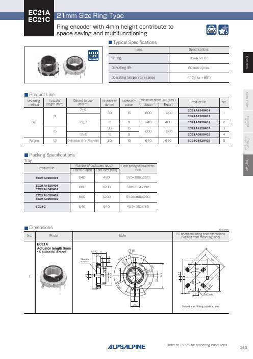
EC21A Actuator length 15mm 9 pulse/18 detent
MAX2630-MAX2633中文资料
_______________General DescriptionThe MAX2630/MAX2631/MAX2632/MAX2633 are low-voltage, low-noise amplifiers for use from VHF to microwave frequencies. Operating from a single +2.7V to +5.5V supply, these devices have a flat gain response to 900MHz. Their low noise figure and low supply current make them ideal for receive, buffer, and transmit IF applications.The MAX2630/MAX2631 are biased internally, eliminat-ing the need for external bias resistors or inductors. The MAX2632/MAX2633 have a user-selectable supply cur-rent, which can be adjusted by adding a single external resistor. This allows customized output power and gain according to specific applications requirements. The MAX2631/MAX2633 feature a shutdown pin that allows them to be powered down to less than 1µA supply cur-rent. Aside from a single bias resistor required for the MAX2632/MAX2633, the only external components needed for this family of amplifiers are input and output blocking capacitors and a V CC bypass capacitor.The MAX2630 comes in a 4-pin SOT143 package, re-quiring minimal board space. The MAX2631/MAX2632come in small 5-pin SOT23 packages. The MAX2633comes in a 6-pin SOT23 package.________________________ApplicationsPersonal Communicating Systems Cordless Phones Global Positioning Systems Cellular Phones Wireless Local Area Networks ISM Radios Wireless Local Loops TV Tuners Land Mobile RadiosSet-Top Boxes____________________________Featureso Single +2.7V to +5.5V Operation o Internally Biased (MAX2630/MAX2631)o Adjustable Bias (MAX2632/MAX2633)o 6.6mA Supply Current (insensitive to supply voltage)o 1µA Shutdown Current (MAX2631/MAX2633)o 3.7dB Noise Figure o 13.4dB Gaino Ultra-Small SOT PackagesMAX2630–MAX2633VHF-to-Microwave, +3V ,General-Purpose Amplifiers________________________________________________________________Maxim Integrated Products1_________________Pin Configurations__________Typical Operating Circuit______________Ordering Information19-1181; Rev 1; 7/97*The first two letters in the SOT top mark identify the part,while the remaining two letters are the lot-tracking code.For free samples & the latest literature: , or phone 1-800-998-8800.For small orders, phone 408-737-7600 ext. 3468.M A X 2630–M A X 2633VHF-to-Microwave, +3V ,General-Purpose Amplifiers 2_______________________________________________________________________________________ABSOLUTE MAXIMUM RATINGSELECTRICAL CHARACTERISTICS(V CC = +3V, Z 0= 50Ω, f IN = 900MHz, R BIAS = 10k Ω(MAX2632/MAX2633), V SHDN = V CC (MAX2631/MAX2633), T A = +25°C, unless otherwise noted.)Stresses beyond those listed under “Absolute Maximum Ratings” may cause permanent damage to the device. These are stress ratings only, and functional operation of the device at these or any other conditions beyond those indicated in the operational sections of the specifications is not implied. Exposure to absolute maximum rating conditions for extended periods may affect device reliability.Note 1:Guaranteed by design and characterization.V CC to GND................................................................-0.3V to 6V Input Power.........................................................................5dBm OUT Current.....................................................................±12mA IN to GND Voltage...................................................-1.2V to 1.2V Bias to GND Voltage....................................................0.0V to 3V Voltage at SHDN Input(MAX2631/MAX2633)............................-0.3V to (V CC + 0.3V)Current into SHDN Input (MAX2631/MAX2633).................100µAContinuous Power Dissipation (T A = +70°C)SOT143 (derate 4mW/°C above +70°C).....................320mW SOT23-5 (derate 7.1mW/°C above +70°C).................571mW SOT23-6 (derate 7.1mW/°C above +70°C).................571mW Operating Temperature Range ...........................-40°C to +85°C Junction Temperature......................................................+150°C Storage Temperature Range.............................-65°C to +150°C Lead Temperature (soldering, 10sec).............................+300°CMAX2630–MAX2633VHF-to-Microwave, +3V ,General-Purpose Amplifiers_______________________________________________________________________________________3__________________________________________Typical Operating Characteristics(V CC = +3V, V SHDN = V CC (MAX2631/MAX2633), Z 0= 50Ω, f IN = 900MHz, R BIAS = 10k Ω(MAX2632/MAX2633), T A = +25°C, unless otherwise noted.)108642023456SUPPLY CURRENT vs. SUPPLY VOLTAGEV CC (V)I C C (m A )252015105005.02.510.015.0MAX2632/MAX2633GAIN vs. SUPPLY CURRENTI CC (mA)G A I N (d B )7.512.52016128400.10.30.71.11.31.5GAIN vs. FREQUENCY AND VOLTAGEFREQUENCY (GHz)G A I N (d B )0.50.9-5.0-7.5-10.0-12.5-15.00.10.30.71.11.31.5OUTPUT 1dB COMPRESSIONPOWER vs. FREQUENCY AND TEMPERATUREFREQUENCY (GHz)P -1 (d B m )0.50.92016128400.10.30.71.11.31.5GAIN vs. FREQUENCYAND TEMPERATUREFREQUENCY (GHz)G A I N (d B )0.50.9-5.0-7.5-10.0-12.5-15.00.10.30.71.11.31.5OUTPUT 1dB COMPRESSIONPOWER vs. FREQUENCY AND VOLTAGEFREQUENCY (GHz)P -1 (d B m )0.50.9-4-8-12-16-202.57.512.515.0MAX2632/MAX2633OUTPUT 1dB COMPRESSION POWER vs. SUPPLY CURRENTI CC (mA)P -1 (d B m )5.010.05432100.10.30.50.91.11.5NOISE FIGURE vs. FREQUENCYM A X 2630-8FREQUENCY (GHz)N O I S E F I G U R E (d B )0.71.3M A X 2630–M A X 2633VHF-to-Microwave, +3V ,General-Purpose Amplifiers 4_____________________________________________________________________________________________________________________________________________________Pin Description15129630110100MAX2632/MAX2633SUPPLY CURRENT vs. R BIASR BIAS (k Ω)I C C (m A)00.010.030.020.040.05-40-2020406080MAX2631/MAX2633SHUTDOWN SUPPLY CURRENTvs. TEMPERATURETEMPERATURE (°C)S H U T D O W N I C C (µA )5:14:13:12:11:10.10.30.7 1.1 1.3 1.5VOLTAGE STANDING-WAVE RATIO vs. FREQUENCYFREQUENCY (GHz)V S W R0.50.9____________________________Typical Operating Characteristics (continued)(V CC = +3V, V SHDN = V CC (MAX2631/MAX2633), Z 0= 50Ω, f IN = 900MHz, R BIAS = 10k Ω(MAX2632/MAX2633), T A = +25°C, unless otherwise noted.)MAX2630–MAX2633VHF-to-Microwave, +3V ,General-Purpose Amplifiers_______________________________________________________________________________________5Table 1a. Typical Scattering Parameters(V CC = +3V, V SHDN = V CC , Z 0= 50Ω, R BIAS = 10k Ω, T A = +25°C.)M A X 2630–M A X 2633VHF-to-Microwave, +3V ,General-Purpose Amplifiers 6_______________________________________________________________________________________Table 1b. MAX2633 Typical Scattering Parameters(V CC = +5V, V SHDN = V CC , Z 0= 50Ω, R BIAS = 10k, T A = +25°C.)MAX2630–MAX2633VHF-to-Microwave, +3V ,General-Purpose Amplifiers_______________________________________________________________________________________7_______________Detailed DescriptionThe MAX2630–MAX2633 are broadband amplifiers with 3dB bandwidth greater than 1GHz. Their small size and internal bias circuitry make them ideal for applications where board space is limited. The MAX2632/MAX2633have a user-selectable bias current that allows the user to set both gain and output power for a particular appli-cation, and the MAX2631/MAX2633 incorporate shut-down capability.__________Applications InformationExternal ComponentsThe MAX2630–MAX2633 are easy to use, as shown in the Typical Operating Circuit and Figures 1, 2 and 3. Input and output series capacitors may be necessary to block DC bias voltages generated by the amplifiers from inter-acting with adjacent circuitry. These capacitors must be large enough to contribute negligible reactance in a 50Ωsystem at the minimum operating frequency. Use the fol-lowing equation to calculate their minimum value:where f (in megahertz) is the minimum operating frequency.The V CC pin must be RF bypassed for correct opera-tion. To accomplish this, connect a capacitor between the V CC pin and ground, as close to the package as is practical. Use the same equation given above (for DC-blocking capacitor values) to calculate the minimum capacitor value. If the PC board has long V CC lines,additional bypassing may be necessary. This can be done farther away from the package, if needed.Proper grounding of the GND pin is essential. If the PC board uses a topside RF ground, connect it directly to the GND pin. For a board where the ground plane is not on the component side, the best technique is to con-nect the GND pin to it with a plated through-hole close to the package.An on-chip buffer at the MAX2631/MAX2633’s SHDN pin makes bypassing this pin unnecessary except in very noisy applications. When RF filtering is needed,use a bypass capacitor similar to the one used on V CC .Since negligible current flows into this pin, additional RF filtering may be done with a series resistor.To set the MAX2632/MAX2633’s supply current,connect a resistor from the BIAS pin to ground. To estimate the value of this resistor, refer to the graph Supply Current vs. R BIAS in the Typical Operating Characteristics .C BLOCK =53,000f(pF)M A X 2630–M A X 2633VHF-to-Microwave, +3V ,General-Purpose Amplifiers 8_______________________________________________________________________________________Figure 4. MAX2630 Example PC Board LayoutFigure 5. MAX2631 Example PC Board LayoutFigure 7. MAX2633 Example PC Board LayoutFigure 6. MAX2632 Example PC Board Layout PC Board Layout ExampleExample PC board layouts are given in Figures 4 to 7.They use FR-4 with a 31mil layer thickness between the RF lines and the ground plane. The boards satisfy all of the above recommendations.MAX2630–MAX2633VHF-to-Microwave, +3V ,General-Purpose Amplifiers_______________________________________________________________________________________9__________________________________________________Tape-and-Reel Information___________________Chip InformationTRANSISTOR COUNT: 199M A X 2630–M A X 2633VHF-to-Microwave, +3V ,General-Purpose Amplifiers 10______________________________________________________________________________________________________________________________________________Package InformationMAX2630–MAX2633VHF-to-Microwave, +3V ,General-Purpose Amplifiers ______________________________________________________________________________________11___________________________________________Package Information (continued)M A X 2630–M A X 2633VHF-to-Microwave, +3V ,General-Purpose Amplifiers___________________________________________Package Information (continued)Maxim cannot assume responsibility for use of any circuitry other than circuitry entirely embodied in a Maxim product. No circuit patent licenses are implied. Maxim reserves the right to change the circuitry and specifications without notice at any time.12____________________Maxim Integrated Products, 120 San Gabriel Drive, Sunnyvale, CA 94086 408-737-7600©1997 Maxim Integrated Products Printed USA is a registered trademark of Maxim Integrated Products.。
MAX262中文资料

M A X262中文资料(总5页) -CAL-FENGHAI.-(YICAI)-Company One1-CAL-本页仅作为文档封面,使用请直接删除在电子电路中,滤波器是不可或缺的部分,其中有源滤波器更为常用。
一般有源滤波器由运算放大器和RC元件组成,对元器件的参数精度要求比较高,设计和调试也比较麻烦。
美国Maxim公司生产的可编程滤波器芯片MAX262可以通过编程对各种低频信号实现低通、高通、带通、带阻以及全通滤波处理,且滤波的特性参数如中心频率、品质因数等,可通过编程进行设置,电路的外围器件也少。
本文介绍MAX262的情况以及由它构成的程控滤波器电路。
1 MAX262芯片介绍MAX262芯片是Maxim公司推出的双二阶通用开关电容有源滤波器,可通过微处理器精确控制滤波器的传递函数(包括设置中心频率、品质因数和工作方式)。
它采用CMOS工艺制造,在不需外部元件的情况下就可以构成各种带通、低通、高通、陷波和全通滤波器。
图1是它的引脚排列情况。
图1 MAX262引脚V+ ——正电源输入端。
V- ——负电源输入端。
GND ——模拟地。
CLKA ——外接晶体振荡器和滤波器A 部分的时钟输入端,在滤波器内部,时钟频率被2分频。
CLKB ——滤波器B 部分的时钟输入端,同样在滤波器内部,时钟频率被2分频。
CLKOUT ——晶体振荡器和R-C振荡的时钟输出端。
OSCOUT ——与晶体振荡器或R-C振荡器相连,用于自同步。
INA、INB ——滤波器的信号输入端。
BPA、BPB——带通滤波器输出端。
LPA、LPB——低通滤波器输出端。
HPA、HPB——高通、带阻、全通滤波器输出端。
WR ——写入有效输入端。
接V+时,输人数据不起作用;接V-时,数据可通过逻辑接口进入一个可编程的内存之中,以完成滤波器的工作模式、f0及Q的设置。
此外,还可以接收TTL电平信号,并上升沿锁存输人数据。
A0、A1、A2、A3 ——地址输人端,可用来完成对滤波器工作模式、f0和Q的相应设置。
Edimax IC-3140W WiFi路由器设置手册(版本2.0)说明书
IC-3140WCopyright @ Edimax Technology Co., Ltd. all rights reserved. No part of this publication may be reproduced, transmitted, transcribed, stored in a retrieval system, or translated into any language or computer language, in any form or by any means, electronic, mechanical, magnetic, optical, chemical, manual or otherwise, without the prior written permission from Edimax Technology Co., Ltd.Edimax Technology Co., Ltd. makes no representations or warranties, either expressed or implied, with respect to the contents hereof and specifically disclaims any warranties, merchantability, or fitness for any particular purpose. Any software described in this manual is sold or licensed as is. Should the programs prove defective following their purchase, the buyer (and not this company, its distributor, or its dealer) assumes the entire cost of all necessary servicing, repair, and any incidental or consequential damages resulting from any defect in the software. Edimax Technology Co., Ltd. reserves the right to revise this publication and to make changes from time to time in the contents hereof without the obligation to notify any person of such revision or changes.The product you have purchased and the setup screen may appear slightly different from those shown in this QIG. For more information about this product, please refer to the user manual on the CD-ROM. The software and specifications are subject to change without notice. Please visit our website for updates. All brand and product names mentioned in this manual are trademarks and/or registered trademarks of their respective holders.Edimax Technology Co., Ltd.Add: No. 3, Wu-Chuan 3rd Rd., Wu-Ku Industrial Park, New Taipei City, TaiwanTel: +886-2-77396888Email: ****************.twNotice According to GNU General Public License Version 2Certain Edimax products include software code developed by third parties, software code is subject to the GNU General Public License ("GPL") or GNU Lesser General Public License ("LGPL"). Please see the GNU () and LPGL() Websites to view the terms of each license.The GPL Code and LGPL Code used in Edimax products are distributed without any warranty and are subject to the copyrights of their authors. For details, see the GPL Code and LGPL Code licenses. You can download the firmware-files at under "Download" page.產品介紹I-1. 包裝內容IC-3140W快速安裝指南 手冊光碟電源變壓器 網路線 壁掛安裝組件I-2. 前面板麥克風PIR (被動式紅外線感測器)LED 指示燈紅外線LED 燈可調焦鏡頭 光線感應器I-3. 背板I-4. LED 指示燈電源指示燈LAN 指示燈Internet 指示燈MAC/Cloud ID 及SetupSSIDLAN 埠電源連接埠WPS/Reset 按鍵MicroSD 卡插槽喇叭I-4. 背板標籤貼紙本產品背面貼有著標籤貼紙,貼紙上印有MAC位址、Cloud ID及Setup SSID等資訊為方便對照使用,本產品的Mac 位址與Cloud ID是一樣的。
Quectel_M26-OpenCPU_硬件设计手册_V1.0
2 综述 ...................................................................................................................................................... 11
3.5.1. 主串口............................................................................................................................. 34
本文档手册版权属于移远公司,任何人未经我公司复制转载该文档将承担法律责任。
Q n 版权所有 ©上海移远通信技术有限公司 2014,保留一切权利。 Confide Copyright © Quectel Wireless Solutions Co., Ltd. 2014
上海移远通信技术有限公司
1 / 81
如需技术支持或反馈我司技术文档中的问题,可随时登陆如下网址: /support/techsupport.aspx
l 前言
移远公司提供该文档内容用以支持其客户的产品设计。客户须按照文档中提供的规范,参数来设计其产品。
te 由于客户操作不当而造成的人身伤害或财产损失,本公司不承担任何责任。在未声明前,移远公司有权对 c l 该文档规范进行更新。 ue tia 版权申明
Q n 3.2.2. 关机 ................................................................................................................................ 26 3.2.2.1. PWRKEY 引脚关机............................................................................................ 26 e 3.2.2.2. API 函数关机...................................................................................................... 27 fid 3.2.2.3. 低压自动关机 ..................................................................................................... 27 3.2.3. 推荐的系统开关机电路 ................................................................................................... 28 3.3. 省电技术 ................................................................................................................................ 29
juniper M系列路由器产品介绍

NEW INSERTION
MPC2E-3D-NG-Q MPC3E-3D-NG
JUNOS Continuity
2nd Generation Trio Higher Scale & Throughput More functionality
MPC3E-3D-NG-Q
MPC3E - 100GE SOLUTION
Software
64bit RPD CPP Hypermode for Web2.0
IPv6 Ready Segment Routing NG vMX
10GE MACSEC vCCAP
Innovation
G.709 OTN Framing
Node Virtualization Scale-out Edge
MPC3 Modular Line Card Applications 130 GbE Card
WAN Edge Services Full MPLS Features All MX Functionality
Experience, Economics & Ecosystem
Up to 5M IP Routes Full scale L3VPN and VPLS Service Rich Processing
NG-MPC2E and MPC3E Line Cards
Universal Supports all types of interfaces JAM First in the Industry to offer Junos Continuity Business Model License based medium scale HQoS option Power Introduces Dynamic Power Management capability Scale & perf Delivers twice the scale as predecessor MPC
使用说明书-max2642evkit-max2643evkit

General DescriptionThe MAX2642/MAX2643 evaluation kits (EV kits) simplify evaluation of the MAX2642 and MAX2643 low-noise amplifiers (LNAs). These kits enable testing of the devices’ performance and require no additional support circuitry. The signal input and output use SMA connectors to facilitate connection of RF test equipment.The MAX2642/MAX2643 EV kits are fully assembled with the MAX2642 or MAX2643 on board, and incorporate input matching components optimized for 900MHz operation.Featureso Easy Evaluation of MAX2642/MAX2643o +2.7V to +5.5V Single-Supply Operation o RF Input and Output Matched to 50Ωat 900MHz o Jumper Included for Gain/Shutdown Setting o Fully Assembled and TestedEvaluate: MAX2642/MAX2643MAX2642/MAX2643 Evaluation Kits________________________________________________________________Maxim Integrated Products 119-1682; Rev 0; 4/00Ordering InformationFor free samples and the latest literature, visit or phone 1-800-998-8800.For small orders, phone 1-800-835-8769.E v a l u a t e : M A X 2642/M A X 2643MAX2642/MAX2643 Evaluation Kits 2_______________________________________________________________________________________Quick StartThe MAX2642/MAX2643 EV kits are fully assembled and factory tested. Follow the instructions in the Connections and Setup section for proper device evaluation.Test Equipment Required•An RF signal generator capable of delivering -10dBm of output power and a frequency range covering the MAX2642/MAX2643 (800MHz to 1000MHz, for exam-ple)•An RF spectrum analyzer that covers the operating frequency range• A DC power supply capable of supplying +2.7V to +5.5V•Two 50Ωcoaxial cables with SMA connectors •An ammeter to measure supply current (optional)• A noise figure meter (optional)• A network analyzer for measuring gain and return loss (optional)Connections and SetupChecking Power Gain1)Connect a DC supply (preset to +3.0V) to the V CC and GND terminals (through an ammeter, if desired)on the EV kit.2)Set the RF generator for an output frequency of 900MHz at a power level of -30dBm. Connect the RF generator ’s output to the RFIN SMA connector.3)Connect the coaxial cable from the RFOUT SMA con-nector to the spectrum analyzer.4)Turn on the DC supply. The supply current should read approximately 5mA (if using an ammeter).5)Activate the RF generator ’s output. A signal on the spectrum analyzer ’s display should indicate a typical gain of +17dB after accounting for cable and board losses.6)Optional: For the MAX2642, set the jumper JU2 to the V CC position. The power gain should now be +3.5dB.7)Optional: Another method of determining gain is by using a network analyzer. This has the advantage of displaying gain vs. a swept frequency band, in addi-tion to displaying input and output return loss. Refer to the user manual of the network analyzer for setup details.Checking Noise FigureNoise figure measurements on low-noise devices such as the MAX2642/MAX2643 are extremely sensitive to board and lab setup losses and parasitics. There are many techniques and precautions for measuring low noise figure. A detailed explanation of these items would exceed the scope of this document. Take into account PC board and external components loss when performing noise-figure measurements. The typical input losses on these EV kits is 0.25dB. For more infor-mation on how to perform this level of noise-figure mea-surement, refer to the noise-figure meter operating manual and to Hewlett Packard ’s application note #57-2,Noise Figure Measurement Accuracy.Layout ConsiderationsGood PC board layout is an essential part of an RF cir-cuit ’s design. The EV kit PC board can serve as a guide for laying out a board using the MAX2642/MAX2643.Generally, the V CC node on the PC board should have a decoupling capacitor located close to the device,and additional capacitors may be needed for long V CC lines. This minimizes supply coupling. Proper grounding of the GND pins is essential. Connect the GND pins to the ground plane either directly, through vias, or both.Evaluate: MAX2642/MAX2643MAX2642/MAX2643 Evaluation Kits_______________________________________________________________________________________3Figure 1. MAX2642/MAX2643 EV Kit SchematicE v a l u a t e : M A X 2642/M A X 2643MAX2642/MAX2643 Evaluation Kits Maxim c annot assume responsibility for use of any c irc uitry other than c irc uitry entirely embodied in a Maxim produc t. No c irc uit patent lic enses are implied. Maxim reserves the right to change the circuitry and specifications without notice at any time.4_____________________Maxim Integrated Products, 120 San Gabriel Drive, Sunnyvale, CA 94086 408-737-7600©2000 Maxim Integrated ProductsPrinted USAis a registered trademark of Maxim Integrated Products.Figure 2. MAX2642/MAX2643 EV Kits Component PlacementGuide—Component SideFigure 3. MAX2642/MAX2643 EV Kits PC Board Layout—Component SideFigure 4. MAX2642/MAX2643 EV Kits PC Board Layout—Ground Plane Layers 2 and 3Figure 5. MAX2642/MAX2643 EV Kits PC Board Layout—Solder Side。
max263翻译

Max263(264)是开关电容有源滤波器设计用于精密滤波应用。
中心频率,Q,工作模式都可以通过输入引脚选择。
Max263不需要用外部元件去实现带通,低通,高通,全通滤波。
max263是专门带通应用程序和包含一个通用运算放大器。
两个第二阶滤波器部分都包含在这两个设备。
通过fclk/f0Max263和267的中心频率可以到达57KHZ,而max264和268可以到达140KHZ。
Max263(264)有28个引脚,max267(268)有24个引脚。
1、滤波器设计软件化2、中心频率32阶可控3、Q值128阶可控4、Q值与f0独立可编程5、f0可达140KHz6、支持+5V和士5V两种供电方式芯片诸引脚功能如下(括号内数字为引脚号):V+(10):供电正极, 并接旁路电容尽量靠近该脚V-(18):供电负极, 并接旁路电容尽量靠近该脚GND(19):模拟地CLKA(13):A单元元时钟输人, 该时钟在芯片内部被二分频CLKB(14):B单元时钟输人, 该时钟在芯片内部被二分频OSC OUT(20):连至晶体, 组成晶振电路(若接时钟信号时, 该脚不连)INA,INB(5,1):滤波器输人BPA,BPB(3,27): 带通输出LPA,LPB(2,28):低通输出HPA,HPB(4,26):高通、带陷、全通输出M0,M1(8,7):模式选择,+5V高,-5V低F0-F4(24,17,23,12,11):时钟与中心频率比值(FCLK/f0)编程端Q0-Q6(15,16,21,22,25,6,9):Q编程端。
1、供给电压士15V2、输入电压士0.3V3、输入电流士50Ma对M0、M1两个管脚编程可使芯片工作于模式1、2、3、4几种方式,对应的功能如表1所示。
时钟与中心频率比值与编码对应如表2所示。
模式1:当我们要实现全极点低通或带通滤波器如切比雪夫、巴特沃斯滤波器时这种模式是很有用的, 有时该模式也用来实现带陷滤波器, 但由于相关零极点位置固定, 使得用作带陷时受到限制。
- 1、下载文档前请自行甄别文档内容的完整性,平台不提供额外的编辑、内容补充、找答案等附加服务。
- 2、"仅部分预览"的文档,不可在线预览部分如存在完整性等问题,可反馈申请退款(可完整预览的文档不适用该条件!)。
- 3、如文档侵犯您的权益,请联系客服反馈,我们会尽快为您处理(人工客服工作时间:9:00-18:30)。
Package Information
MAX263/MAX264/MAX267/MAX268Pin Programmable Universal and Bandwidth Filters (The package drawing(s) in this data sheet may not reflect the most current specifications. For the latest package outline information
go to /packages.)
M A X 263/M A X 264/M A X 267/M A X 268
Pin Programmable
Universal and Bandwidth Filters 24______________________________________________________________________________________
Package Information (continued)
(The package drawing(s) in this data sheet may not reflect the most current specifications. For the latest package outline information go to /packages .)
Package Information (continued)
MAX263/MAX264/MAX267/MAX268Pin Programmable Universal and Bandwidth Filters (The package drawing(s) in this data sheet may not reflect the most current specifications. For the latest package outline information
go to /packages.)
M A X 263/M A X 264/M A X 267/M A X 268
Pin Programmable
Universal and Bandwidth Filters 26______________________________________________________________________________________
Package Information (continued)
(The package drawing(s) in this data sheet may not reflect the most current specifications. For the latest package outline information go to /packages .)
MAX263/MAX264/MAX267/MAX268
Pin Programmable
Universal and Bandwidth Filters
______________________________________________________________________________________27
Package Information (continued)
(The package drawing(s) in this data sheet may not reflect the most current specifications. For the latest package outline information go to /packages
.)
M A X 263/M A X 264/M A X 267/M A X 268
Pin Programmable
Universal and Bandwidth Filters Maxim cannot assum e responsibility for use of any circuitry other than circuitry entirely em bodied in a Maxim product. No circuit patent licenses are implied. Maxim reserves the right to change the circuitry and specifications without notice at any time.
28____________________Maxim Integrated Products, 120 San Gabriel Drive, Sunnyvale, CA 94086 408-737-7600©2008 Maxim Integrated Products
is a registered trademark of Maxim Integrated Products, Inc.。