MAX4643EUA-T中文资料
MAX产品后缀说明

MAX 产品后缀说明MAX 产品后缀说明三位后缀例: MAX1675E U A温度范围封装形式管脚数四位后缀另有一些MAXIM 产品后缀用四位表示,第一位表示产品精度等级;第二位表示温度范围:精度,后三位同三位后缀的IC.第三位表示封装形式;第四位表示产品管脚数。
例如:MAX631ACPA 第一个”A”表示5%的输出温度范围C 0°C - 70°C A -40°C - +125°CI -20°C - +85°C M -55 °C - +125°CE -40°C - +85°C封装形式A SSOP(密脚表面贴装)B CERQUAD(陶瓷方形封装)C TO220,TQFP(薄的四方表贴封装)D 陶瓷SB 封装E QSOP(四方表面贴封装)F 陶瓷Flat 封装H 模块SBGA 5*5TQFP J 陶瓷双列直插K SOT L LCCM MQFP(公制四方扁平封装) N 窄体陶瓷双列直插P 塑封DIP(双列直插) Q PLCCR 窄体陶瓷DIP S SO 表面贴封装T TO5,TO99,TO100 U TSSOP,uMAX,SOTV TO39 W 宽体SOX SC70 Y 窄SBZ TO92,MQUAD /D DICE(裸片)/PR 硬塑料/W 晶原管脚数A 8 N 18B 10,64 O 42C 12,192 P 20D 14 Q 2,100E 16 R 3,84F 22,256 S 4,80G 24 T 6,160H 44 U 38,60I 28 V 8(圆脚,隔离型)J 32 W 10(圆脚,隔离型)K 5,68 X 8L 40 Y 8(圆脚,隔离型)M 7,48 Z 10(圆脚,隔离型)。
MAX4313EUA+T中文资料
元器件交易网
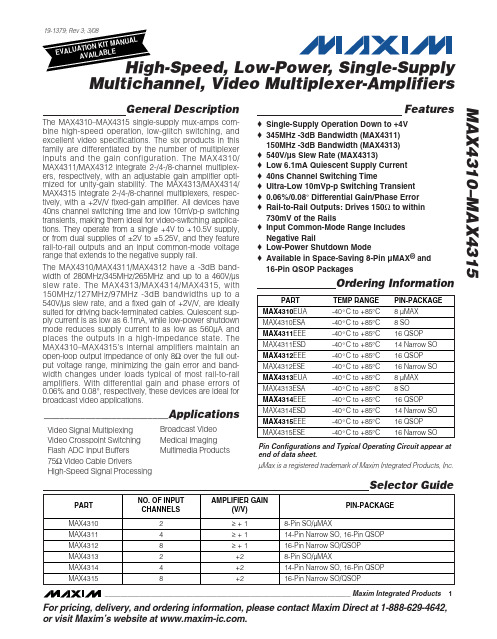
MAX4310–MAX4315
High-Speed, Low-Power, Single-Supply Multichannel, Video Multiplexer-Amplifiers
ABSOLUTE MAXIMUM RATINGS
Supply Voltage (VCC to VEE) .................................................12V Input Voltage....................................(VEE - 0.3V) to (VCC + 0.3V) All Other Pins ...................................(VEE - 0.3V) to (VCC + 0.3V) Output Current................................................................±120mA Short-Circuit Duration (VOUT to GND, VCC or VEE)....Continuous Continuous Power Dissipation (TA = +70°C)
________________________________________________________________ Maxim Integrated Products 1
For pricing, delivery, and ordering information, please contact Maxim Direct at 1-888-629-4642, or visit Maxim’s website at .
46436中文资料

46436 R ight AngleReceptacle46562 Vertical Receptacle 46437 Right Angle PlugSPECIFICATIONS ORDERING INFORMATIONFeatures and Benefits n L ow-profile design of 10.00mm height enhances system airflow and provides 278.0A per linear inch n M odular assembly for virtually any design configuration including wire-to-board options n Right-angle and vertical mounting available for either coplanar or perpendicular applications n Robust, high-current contact blades for DC (5.50mm pitch) and AC (7.50mm pitch) spacing optionsReference Information Packaging: Tray UL File No.: E29179 CSA File No.: LR19880 TUV: R 72081037Designed In: Millimeters Electrical Voltage:Power - 600V max.Current (at 30°C Temperature rise): Power – 60.0A max. Signal – 2.5A max.Contact Resistance (per contact):Initial End of LifePower (milliohms) – 0.50 0.75 max change Signal (milliohms) – 6.50 15.00 max change Dielectric Withstanding Voltage: 1500V Insulation Resistance: 5000 Megohms min.Current interruptions rating: Power – Contact Molex Signal – Contact Molexn Rated for current interruption n C onnectors comply to EIA-364-1001.01 and MFG test procedures n Last-mate/first-break available on both power and signal contacts n 60.0A per power bladeMechanical Pitch:Power – 5.50 or 7.50mm Signal – 2.54 by 2.45mm Mating Force (max. per circuit): Power Contacts – 500g (1.102 lb) Signal Contacts – 102g (.225 lb)Un-mating Force (min. per circuit): Power Contacts – 400g (.882 lb) Signal Contacts – 30g (.066 lb)Durability: 100 cycles PhysicalHousing: 30% glass filled LCP Contact:Power Contacts - Copper Alloy Signal Contacts – Copper Alloy Plating:Contact Area — Select Gold Solder Tail Area — Tin Underplating — Nickel Flammability Rating: UL 94V-0RoHS compliantDocumentsSales Drawings: SD-46436-XXX, SD-46562-XXX SD-46437-XXXProduct Specs: PS-46436-100Series*Description Power CircuitsSignal CircuitsGuideBoard PegPCB Thickness46436Right Angle Receptacle 1 to 106 to 36Side or Top OptionsavailableOptional1.57 to 3.81mm (.062 to .150”)46562Vertical Receptacle46437Plug*Complete part numbers can be found at /link/ext-power.htmlThe EXTreme Ten60 Power™ Connector features the highest square-inch current density of any power connector system that Molex has developed. A low 10.00mm (.394”) profile, coupled with high-capacity power blades, allows this interconnect to target smaller power supply architectures that deliver very high current in limited spaces where airflow can otherwise be restricted by larger connectors. Optional guides can be placed on each end at traditional side locations, or on top of the connector to save valuable PC board real estate. Power and signal modules can be placed in any location.40.035.030.025.020.015.010.05.0Temperature Rise vs. Current per EIA-364-70Current (Amp)30.035.040.045.050.055.060.0T e m p e r a t u r e (°C )8 circuit setup 4 circuit setup 2 circuit setup0.02000.01800.01600.01400.01200.01000.00800.00600.00400.00200.0000V-drop (max) vs. Current per EIA-364-70Current (Amp)30.035.040.045.050.055.060.0V o l t a g e (V )/link/ext-power.htmlOrder No. 987650-3003USA/KC/2009.03© 2009, MolexFEATURES AND SPECIFICATIONSEXTreme Power ® ProductsEXTreme Power ® ProductsThe need for high-current power interconnect solutions in increasingly smaller space continues to rise rapidly. Solving this power equation on new architectures and system platforms has been a major focus for Molex product development teams. The new Molex EXTreme Power ® family of products is the direct result of listening intently to our customers’ electrical and mechanical design challenges. Since no two applications are the same, the Molex EXTreme Power ® offering is comprised of several product families that cover a wide range of current densities, mechanical envelopes, mating terminations and configuration choices that give system designers the ability to maximize their power interconnect needs.50.0 A / Contact 215.0 A / Sq. in.33.0 A / Sq. cm10.00mm16.0 A / Blade 618.0 A / Sq. in.96.0 A / Sq. cm4.00mm40.0 A / Blade 445.0 A / Sq. in.68.0 A / Sq. cm15.00mm30.0 A / Blade 203.0 A / Sq. in.31.0 A / Sq. cm14.58mm30.0 A / Blade 431.0 A / Sq. in.67.0 A / Sq. cm7.50mm60.0 A / Blade 705.0 A / Sq. in.109.0 A / Sq. cm10.00mm150.0 A / Blade 372.0 A / Sq. in.58.0 A / Sq. cm25.00mmEXTreme MicroPower™EXTreme MicroPower™EXTreme PowerEdge™EXTreme PowerPlus™ (SSI)EXTreme LPHPower™EXTreme Ten60Power™EXTreme PowerMass™。
MAX4642EUA-T中文资料

For pricing delivery, and ordering information please contact Maxim/Dallas Direct!at 1-888-629-4642, or visit Maxim’s website at .General DescriptionThe MAX4641/MAX4642/MAX4643 are monolithic, dual,single-pole/single-throw (SPST) switches that can operate from a single supply ranging from +1.8V to +5.5V. The MAX4641/MAX4642/MAX4643 provide low 4Ωon-resis-tance (R ON ), 0.6ΩR ON matching between channels, and 1ΩR ON flatness over the entire analog signal range.These devices offer fast switching times of less than 20ns while consuming less than 0.01µW of quiescent power.The MAX4641 has two normally open (NO) switches,and the MAX4642 has two normally closed (NC)switches. The MAX4643 has one NO switch and one NC switch. All three devices have low 0.35nA leakage cur-rents over the entire temperature range. The MAX4641/MAX4642/MAX4643 are available in small 8-pin µMAX and 8-pin QFN packages.ApplicationsBattery-Operated Equipment Audio and Video Signal Routing Low-Voltage Data-Acquisition Systems Sample-and-Hold Circuits Communications CircuitsFeatureso +1.8V to +5.5V Single-Supply Operation o Rail-to-Rail™Analog Signal Range o Guaranteed R ON4Ωmax (+5V supply)8Ωmax (+3V supply)o +1.8V OperationR ON 30Ωtyp Over Temperature t ON 18ns typ, t OFF 12ns typo Guaranteed R ON Flatness: 1Ω(+5V supply)o Guaranteed R ON Match Between Channels0.6Ω(+5V supply)o Low Leakage (<0.35nA) Over Entire Temperature Rangeo Excellent AC CharacteristicsLow Crosstalk:-97dB at 1MHz High Off-Isolation:-80dB at 1MHz 0.018% Total Harmonic Distortion o Low Power Consumption: < 0.01µWMAX4641/MAX4642/MAX4643High-Speed, Low-Voltage, 4Ω, Dual SPSTCMOS Analog Switches________________________________________________________________Maxim Integrated Products1Pin Configurations/Functional Diagrams/Truth Tables19-1656; Rev 1; 2/02Ordering InformationRail-to-Rail is a trademark of Nippon Motorola, Ltd.M A X 4641/M A X 4642/M A X 4643High-Speed, Low-Voltage, 4Ω, Dual SPST CMOS Analog Switches 2_______________________________________________________________________________________ABSOLUTE MAXIMUM RATINGSELECTRICAL CHARACTERISTICS—Single +5V Supply(V+ = +4.5V to +5.5V, V INH = 2.4V, V INL = 0.8V, T A = T MIN to T MAX , unless otherwise noted. Typical values are at T A = +25°C.)Stresses beyond those listed under “Absolute Maximum Ratings” may cause permanent damage to the device. These are stress ratings only, and functional operation of the device at these or any other conditions beyond those indicated in the operational sections of the specifications is not implied. Exposure to absolute maximum rating conditions for extended periods may affect device reliability.(All Voltages Referenced to GND)V+.............................................................................-0.3V to +6V IN_, COM_, NO_, NC_ (Note 1)....................-0.3V to (V+ + 0.3V)Continuous Current (any terminal)....................................±20mA Continuous Current (NO_, NC_, COM_)...........................±50mA Peak Current (NO_, NC_, COM_, pulsed at 1ms,10% duty cycle)........................................................±100mAContinuous Power Dissipation (T A = +70°C)8-Pin µMAX (derate 4.5mW/°C above +70°C)...........362mW 8-Pin QFN (derate 24.4mW/°C above +70°C).........1951mW Operating Temperature Range ...........................-40°C to +85°C Junction Temperature......................................................+150°C Storage Temperature Range.............................-65°C to +150°C Lead Temperature (soldering, 10s)................................+300°CNote 1:Signals on NO_, NC_, COM_, or IN_ exceeding V+ or GND are clamped by internal diodes. Limit forward-diode current tomaximum current rating.MAX4641/MAX4642/MAX4643High-Speed, Low-Voltage, 4Ω, Dual SPSTCMOS Analog SwitchesELECTRICAL CHARACTERISTICS—Single +5V Supply (continued)(V+ = +4.5V to +5.5V, V INH = 2.4V, V INL = 0.8V, T A = T MIN to T MAX , unless otherwise noted. Typical values are at T A = +25°C.)ELECTRICAL CHARACTERISTICS—Single +3V Supply(V+ = +2.7V to +3.3V, V INH = 2.0V, V INL = 0.4V, T A = T MIN to T MAX , unless otherwise noted. Typical values are at T A = +25°C.)M A X 4641/M A X 4642/M A X 4643High-Speed, Low-Voltage, 4Ω, Dual SPST CMOS Analog Switches 4_______________________________________________________________________________________ELECTRICAL CHARACTERISTICS—Single +3V Supply (continued)(V+ = +2.7V to +3.3V, V INH = 2.0V, V INL = 0.4V, T A = T MIN to T MAX , unless otherwise noted. Typical values are at T A = +25°C.)Note 2:∆R ON = R ON(MAX)- R ON(MIN).Note 3:R ON Flatness is defined as the difference between the maximum and minimum value of on-resistance as measured over thespecified analog signal range.Note 4:Guaranteed by design.Note 5:On-Leakage performed with voltage applied to COM_, with NO_ and NC_ left floating.Note 6:Off-Isolation = 20log 10(V O_ / V I_), where V O is V COM_and V I is V NC_or V NO_from the network analyzer.Note 7:Crosstalk is measured between the two switches.Note 8:R ON and ∆R ON matching specifications for QFN-packaged parts are guaranteed by design.MAX4641/MAX4642/MAX4643High-Speed, Low-Voltage, 4Ω, Dual SPSTCMOS Analog Switches_______________________________________________________________________________________501545306075CHARGE INJECTION vs. V COMV COM (V)C H A R G E I N J E C T I O N (p C )3421520151050021345ON-RESISTANCE vs. V COMV COM (V)R O N (Ω)R O N (Ω)54321-4010-15356085ON-RESISTANCE vs. TEMPERATURETEMPERATURE (°C)1-40853560-1510ON-/OFF-LEAKAGE CURRENTvs. TEMPERATURE100010100TEMPERATURE (°C)L E A K A G E (p A )040208060120100140SUPPLY CURRENT vs. SUPPLY VOLTAGESUPPLY VOLTAGE (V)S U P P L Y C U R R E N T (n A )1.82.83.84.85.82.01.51.00.501.83.42.64.25.05.8LOGIC THRESHOLD vs. SUPPLY VOLTAGEM A X 4641/2/3t o c 06SUPPLY VOLTAGE (V)L O G I C T H R E S H O L D (V )03961215SWITCHING TIMES vs. SUPPLY VOLTAGET O C 4641/2/3t o c 07SUPPLY VOLTAGE (V)S W I T C H I N G T I M E S (n s )24350264810SWITCHING TIMES vs. TEMPERATURETEMPERATURE (°C)S W I T C H I N G T I M E S (n s )-40356010-1585300250200150100500-4010-15356085SUPPLY CURRENT vs. TEMPERATURETEMPERATURE (°C)S U P P L Y C U R R E N T (n A )Typical Operating Characteristics(V+ = +5V or +3V, V INH = V+, V INL = GND, T A = +25°C, unless otherwise noted.)M A X 4641/M A X 4642/M A X 4643High-Speed, Low-Voltage, 4Ω, Dual SPST CMOS Analog Switches 6_______________________________________________________________________________________Typical Operating Characteristics (continued)(V+ = +5V or +3V, V INH = V+, V INL = GND, T A = +25°C, unless otherwise noted.)Pin Description00.010.11101001000-10-40-50-30-20-60-70-80-90-100FREQUENCY RESPONSEFREQUENCY (MHz)(d B /d i v )00.011100.1100M A X 4641/2/3t o c 11FREQUENCY (MHz)C R O S S T A L K (d B )-100-80-60-40-20CROSSTALK vs. FREQUENCY0.050.011100.1100TOTAL HARMONIC DISTORTIONvs. FREQUENCYFREQUENCY (kHz)T H D (%)00.010.020.030.04Note:NO_, NC_, and COM_ pins are identical and interchangeable. Signals can be passed through either side of these bidirectional switches. However, the typical off-capacitances differ, as shown in the Electrical Characteristics.MAX4641/MAX4642/MAX4643High-Speed, Low-Voltage, 4Ω, Dual SPSTCMOS Analog Switches_______________________________________________________________________________________7Applications InformationThe MAX4641/MAX4642/MAX4643 operate from a sin-gle supply ranging from +1.8V to +5.5V. The devices are guaranteed to be functional over that supply range,but TTL /CMOS compatibility is only valid for operation using a +5V supply. All voltage levels are referenced to GND. Positive and negative DC analog inputs or AC signals can be accommodated by shifting V+ and GND.ESD-protection diodes are internally connected be-tween each analog-signal pin and both V+ and GND.One of these diodes conducts if any analog signalexceeds V+ or GND (Figure 1). Virtually all of the ana-log leakage current comes from the ESD diodes to V+or GND. Although the ESD diodes on a given signal pin are identical, and therefore fairly well balanced, they are reverse biased differently. Each is biased by either V+ or GND and the analog signal. This means their leakages will vary as the signal varies. The difference in the two diode leakages to the V+ and GND pins consti-tutes the analog-signal-path leakage current. All analog leakage current flows between each pin and one of the supply terminals, not to the other switch terminal. This is why both sides of a given switch can show leakage currents of the same or opposite polarity.There is no normal current path between the analog-signal paths and V+ or GND. V+ and GND also power the internal logic and logic-level translators. The logic-level translators convert the logic level into switched V+and GND signals to drive the analog signal gates.Figure 1. Overvoltage Protection Using External Blocking DiodesPin Configurations/Functional Diagrams/Truth Tables (continued)M A X 4641/M A X 4642/M A X 4643High-Speed, Low-Voltage, 4Ω, Dual SPST CMOS Analog Switches 8_______________________________________________________________________________________Figure 2. Switching TimesMAX4641/MAX4642/MAX4643High-Speed, Low-Voltage, 4Ω, Dual SPSTCMOS Analog Switches_______________________________________________________________________________________9Figure 5. NO_, NC_, and COM_ CapacitanceFigure 3. Off-Isolation, On-Loss, and CrosstalkFigure 4. Charge InjectionChip InformationTRANSISTOR COUNT: 105M A X 4641/M A X 4642/M A X 4643High-Speed, Low-Voltage, 4Ω, Dual SPST CMOS Analog Switches Ma xim ca nnot a ssume responsibility for use of a ny circuitry other tha n circuitry entirely embodied in a Ma xim product. No circuit pa tent licenses a re implied. Maxim reserves the right to change the circuitry and specifications without notice at any time.10____________________Maxim Integrated Products, 120 San Gabriel Drive, Sunnyvale, CA 94086 408-737-7600©2002 Maxim Integrated ProductsPrinted USAis a registered trademark of Maxim Integrated Products.Package Information。
MAX465中文资料

PART
DESCRIPΒιβλιοθήκη IONMAX463 MAX464 MAX465 MAX466 MAX467 MAX468 MAX469 MAX470
Triple RGB Switch & Buffer Quad RGB Switch & Buffer Triple RGB Switch & Buffer Quad RGB Switch & Buffer Triple Video Buffer Quad Video Buffer Triple Video Buffer Quad Video Buffer
Continuous Power Dissipation (TA = +70°C) 16-Pin Plastic DIP (derate 22.22mW/°C above +70°C) ....1778mW 16-Pin Wide SO (derate 20.00mW/°C above +70°C) .......1600mW
The MAX463–MAX470 series of two-channel, triple/quad buffered video switches and video buffers combines high-accuracy, unity-gain-stable amplifiers with high-performance video switches. Fast switching time and low differential gain and phase error make this series of switches and buffers ideal for all video applications. The devices are all specified for ±5V supply operation with inputs and outputs as high as ±2.5V when driving 150Ω loads (75Ω back-terminated cable).
max485esa中文资料
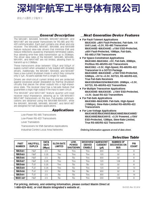
General DescriptionThe MAX481, MAX483, MAX485, MAX487–MAX491, andMAX1487 are low-power transceivers for RS-485 and RS-422 communication. Each part contains one driver and onereceiver. The MAX483, MAX487, MAX488, and MAX489feature reduced slew-rate drivers that minimize E MI andreduce reflections caused by improperly terminated cables,thus allowing error-free data transmission up to 250kbps.The driver slew rates of the MAX481, MAX485, MAX490,MAX491, and MAX1487 are not limited, allowing them totransmit up to 2.5Mbps.These transceivers draw between 120µA and 500µA ofsupply current when unloaded or fully loaded with disableddrivers. Additionally, the MAX481, MAX483, and MAX487have a low-current shutdown mode in which they consumeonly 0.1µA. All parts operate from a single 5V supply.Drivers are short-circuit current limited and are protectedagainst excessive power dissipation by thermal shutdowncircuitry that places the driver outputs into a high-imped-ance state. The receiver input has a fail-safe feature thatguarantees a logic-high output if the input is open circuit.The MAX487 and MAX1487 feature quarter-unit-loadreceiver input impedance, allowing up to 128 MAX487/MAX1487 transceivers on the bus. Full-duplex communi-cations are obtained using the MAX488–MAX491, whilethe MAX481, MAX483, MAX485, MAX487, and MAX1487are designed for half-duplex applications.________________________Applications Low-Power RS-485 Transceivers Low-Power RS-422 Transceivers Level Translators Transceivers for EMI-Sensitive Applications Industrial-Control Local Area Networks__Next Generation Device Features o For Fault-Tolerant Applications MAX3430: ±80V Fault-Protected, Fail-Safe, 1/4Unit Load, +3.3V, RS-485 Transceiver MAX3440E–MAX3444E: ±15kV ESD-Protected,±60V Fault-Protected, 10Mbps, Fail-Safe, RS-485/J1708 Transceivers o For Space-Constrained Applications MAX3460–MAX3464: +5V, Fail-Safe, 20Mbps,Profibus RS-485/RS-422 Transceivers MAX3362: +3.3V, High-Speed, RS-485/RS-422Transceiver in a SOT23 Package MAX3280E–MAX3284E: ±15kV ESD-Protected,52Mbps, +3V to +5.5V, SOT23, RS-485/RS-422,True Fail-Safe Receivers MAX3293/MAX3294/MAX3295: 20Mbps, +3.3V,SOT23, RS-485/RS-422 Transmitters o For Multiple Transceiver Applications MAX3030E–MAX3033E: ±15kV ESD-Protected,+3.3V, Quad RS-422 Transmitters o For Fail-Safe Applications MAX3080–MAX3089: Fail-Safe, High-Speed (10Mbps), Slew-Rate-Limited RS-485/RS-422Transceiverso For Low-Voltage ApplicationsMAX3483E/MAX3485E/MAX3486E/MAX3488E/MAX3490E/MAX3491E: +3.3V Powered, ±15kVESD-Protected, 12Mbps, Slew-Rate-Limited,True RS-485/RS-422 Transceivers For pricing, delivery, and ordering information, please contact Maxim Direct at1-888-629-4642, or visit Maxim Integrated’s website at .______________________________________________________________Selection Table19-0122; Rev 10; 9/14PARTNUMBERHALF/FULL DUPLEX DATA RATE (Mbps) SLEW-RATE LIMITED LOW-POWER SHUTDOWN RECEIVER/DRIVER ENABLE QUIESCENT CURRENT (μA) NUMBER OF RECEIVERS ON BUS PIN COUNT MAX481Half 2.5No Yes Yes 300328MAX483Half 0.25Yes Yes Yes 120328MAX485Half 2.5No No Yes 300328MAX487Half 0.25Yes Yes Yes 1201288MAX488Full 0.25Yes No No 120328MAX489Full 0.25Yes No Yes 1203214MAX490Full 2.5No No No 300328MAX491Full 2.5No No Yes 3003214MAX1487 Half 2.5No No Yes 2301288Ordering Information appears at end of data sheet.找电子元器件上宇航军工MAX481/MAX483/MAX485/MAX487–MAX491/MAX1487Low-Power, Slew-Rate-LimitedRS-485/RS-422 TransceiversPackage Information For the latest package outline information and land patterns, go to . Note that a “+”, “#”, or “-”in the package code indicates RoHS status only. Package drawings may show a different suffix character, but the drawing pertains to the package regardless of RoHS status.16Low-Power, Slew-Rate-Limited RS-485/RS-422 TransceiversMAX481/MAX483/MAX485/MAX487–MAX491/MAX1487Maxim Integrated cannot assume responsibility for use of any circuitry other than circuitry entirely embodied in a Maxim Integrated product. No circuit patent licenses are implied. Maxim Integrated reserves the right to change the circuitry and specifications without notice at any time. The parametric values (min and max limits) shown in the Electrical Characteristics table are guaranteed. Other parametric values quoted in this data sheet are provided for guidance.Maxim Integrated 160 Rio Robles, San Jose, CA 95134 USA 1-408-601-100017©2014 Maxim Integrated Products, Inc.Maxim Integrated and the Maxim Integrated logo are trademarks of Maxim Integrated Products, Inc.。
MEMORY存储芯片MAX3490EESA+T中文规格书

Figure 1. MAX3483/MAX3485/MAX3486 Pin Configuration and Typical Operating Circuit Figure 2. MAX3488/MAX3490 Pin Configuration and Typical Operating Circuit Figure 3. MAX3491 Pin Configuration and Typical Operating CircuitMAX3483/MAX3485/MAX3486/MAX3488/MAX3490/MAX34913.3V-Powered, 10Mbps and Slew-Rate-Limited True RS-485/RS-422 TransceiversDriver Output ProtectionExcessive output current and power dissipation caused by faults or by bus contention are prevented by two mechanisms. A foldback current limit on the output stage provides immediate protection against short circuits over the whole common-mode voltage range (see Typical Operating Characteristics ). In addition, a thermal shut-down circuit forces the driver outputs into a high-impedance state if the die temperature rises excessively.Propagation Delay Figures 15–18 show the typical propagation delays. Skew time is simply the difference between the low-to-high and high-to-low propagation delay. Small driver/receiver skew times help maintain a symmetrical mark-space ratio (50% duty cycle).The receiver skew time, |t PRLH - t PRHL |, is under 10ns (20ns for the MAX3483/MAX3488). The driver skew times are 8ns for the MAX3485/MAX3490/MAX3491, 11ns for the MAX3486, and typically under 100ns for the MAX3483/MAX3488.Line Length vs. Data Rate The RS-485/RS-422 standard covers line lengths up to 4000 feet. For line lengths greater than 4000 feet, see Figure 23.Figures 19 and 20 show the system differential voltage for parts driving 4000 feet of 26AWG twisted-pair wire at 125kHz into 120Ω loads.Typical ApplicationsThe MAX3483, MAX3485, MAX3486, MAX3488, MAX3490, and MAX3491 transceivers are designed for bidirectional data communications on multipoint bus transmission lines. Figures 21 and 22 show typical net-work applications circuits. These parts can also be used as line repeaters, with cable lengths longer than 4000 feet, as shown in Figure 23.To minimize reflections, the line should be terminated at both ends in its characteristic impedance, and stub lengths off the main line should be kept as short as pos-sible. The slew-rate-limited MAX3483/MAX3488 and the partially slew-rate-limited MAX3486 are more tolerant of imperfect termination.Figure 21. MAX3483/MAX3485/MAX3486 Typical RS-485 NetworkMAX3483/MAX3485/MAX3486/MAX3488/MAX3490/MAX34913.3V-Powered, 10Mbps and Slew-Rate-Limited True RS-485/RS-422 Transceivers。
MEMORY存储芯片MAX4053ESE+T中文规格书
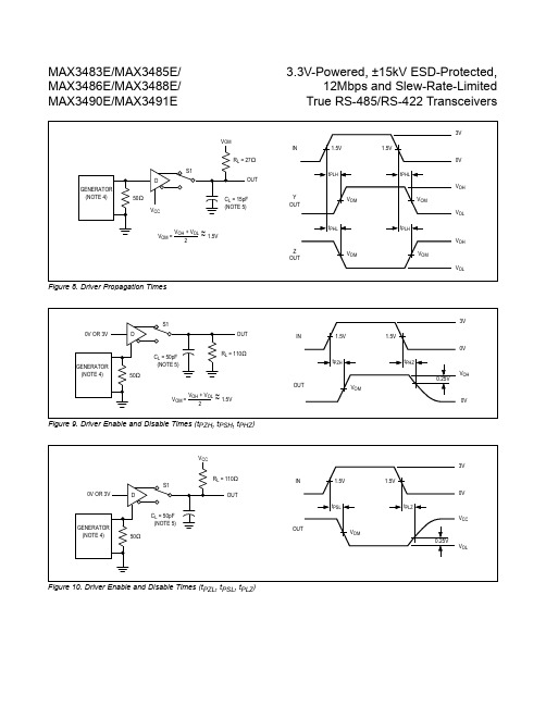
Figure 8. Driver Propagation TimesFigure 9. Driver Enable and Disable Times (t PZH , t PSH , t PHZ )Figure 10. Driver Enable and Disable Times (t PZL , t PSL , t PLZ )MAX3483E/MAX3485E/MAX3486E/MAX3488E/MAX3490E/MAX3491E3.3V-Powered, ±15kV ESD-Protected, 12Mbps and Slew-Rate-Limited True RS-485/RS-422 TransceiversDriver Output ProtectionExcessive output current and power dissipation caused by faults or by bus contention are prevented by two mechanisms. A foldback current limit on the output stage provides immediate protection against short circuits over the whole common-mode voltage range (see Typical Operating Characteristics ). In addition, a thermal shut-down circuit forces the driver outputs into a high-imped-ance state if the die temperature rises excessively.Propagation DelayFigures 15–18 show the typical propagation delays. Skew time is simply the difference between the low-to-high and high-to-low propagation delay. Small driver/receiver skew times help maintain a symmetrical mark-space ratio (50% duty cycle).The receiver skew time, |tPRLH - t PRHL |, is under 10ns 20ns for the MAX3483E/MAX3488E). The driver skew times are 8ns for the MAX3485E/MAX3490E/MAX3491E, 12ns for the MAX3486E, and typically under 50ns for the MAX3483E/MAX3488E.Line Length vs. Data RateThe RS-485/RS-422 standard covers line lengths up to 4000 feet. For line lengths greater than 4000 feet, see Figure 21 for an example of a line repeater.Figures 19 and 20 show the system differential voltage for parts driving 4000 feet of 26AWG twisted-pair wire at 125kHz into 120Ω loads.For faster data rate transmission, please consult the factory.±15kV ESD Protection As with all Maxim devices, ESD-protection structures are incorporated on all pins to protect against electrostatic discharges encountered during handling and assembly. The driver outputs and receiver inputs of the MAX3483E family of devices have extra protection against static electricity. Maxim’s engineers have developed state-of-the-art structures to protect these pins against ESD of ±15kV without damage. The ESD structures withstand high ESD in all states: normal operation, shutdown, and powered down. After an ESD event, Maxim’s E versions keep working without latchup or damage.ESD protection can be tested in various ways; the trans-mitter outputs and receiver inputs of this product family are characterized for protection to the following limits:1)±15kV using the Human Body Model 2)±8kV using the Contact-Discharge method specified in IEC 1000-4-23)±15kV using IEC 1000-4-2’s Air-Gap method.ESD Test Conditions ESD performance depends on a variety of conditions. Contact Maxim for a reliability report that documents test setup, test methodology, and test results.Human Body Model Figure 22a shows the Human Body Model and Figure 22b shows the current waveform it generates when dis-charged into a low impedance. This model consists of a 100pF capacitor charged to the ESD voltage of interest, which is then discharged into the test device through a 1.5kΩ resistor.IEC 1000-4-2The IEC 1000-4-2 standard covers ESD testing and performance of finished equipment; it does not specifi-cally refer to integrated circuits. The MAX3483E family of devices helps you design equipment that meets Level 4 (the highest level) of IEC 1000-4-2, without the need for additional ESD-protection components.The major difference between tests done using the Human Body Model and IEC 1000-4-2 is higher peak cur-rent in IEC 1000-4-2, because series resistance is lower in the IEC 1000-4-2 model. Hence, the ESD withstand voltage measured to IEC 1000-4-2 is generally lower than that measured using the Human Body Model. Figure 23a shows the IEC 1000-4-2 model, and Figure 23b shows the current waveform for the ±8kV IEC 1000-4-2, Level 4ESD contact-discharge test. test.Figure 21. Line Repeater for MAX3488E/MAX3490E/MAX3491EMAX3483E/MAX3485E/MAX3486E/MAX3488E/MAX3490E/MAX3491E3.3V-Powered, ±15kV ESD-Protected, 12Mbps and Slew-Rate-Limited True RS-485/RS-422 Transceivers。
- 1、下载文档前请自行甄别文档内容的完整性,平台不提供额外的编辑、内容补充、找答案等附加服务。
- 2、"仅部分预览"的文档,不可在线预览部分如存在完整性等问题,可反馈申请退款(可完整预览的文档不适用该条件!)。
- 3、如文档侵犯您的权益,请联系客服反馈,我们会尽快为您处理(人工客服工作时间:9:00-18:30)。
For pricing delivery, and ordering information please contact Maxim/Dallas Direct!at 1-888-629-4642, or visit Maxim’s website at .General DescriptionThe MAX4641/MAX4642/MAX4643 are monolithic, dual,single-pole/single-throw (SPST) switches that can operate from a single supply ranging from +1.8V to +5.5V. The MAX4641/MAX4642/MAX4643 provide low 4Ωon-resis-tance (R ON ), 0.6ΩR ON matching between channels, and 1ΩR ON flatness over the entire analog signal range.These devices offer fast switching times of less than 20ns while consuming less than 0.01µW of quiescent power.The MAX4641 has two normally open (NO) switches,and the MAX4642 has two normally closed (NC)switches. The MAX4643 has one NO switch and one NC switch. All three devices have low 0.35nA leakage cur-rents over the entire temperature range. The MAX4641/MAX4642/MAX4643 are available in small 8-pin µMAX and 8-pin QFN packages.ApplicationsBattery-Operated Equipment Audio and Video Signal Routing Low-Voltage Data-Acquisition Systems Sample-and-Hold Circuits Communications CircuitsFeatureso +1.8V to +5.5V Single-Supply Operation o Rail-to-Rail™Analog Signal Range o Guaranteed R ON4Ωmax (+5V supply)8Ωmax (+3V supply)o +1.8V OperationR ON 30Ωtyp Over Temperature t ON 18ns typ, t OFF 12ns typo Guaranteed R ON Flatness: 1Ω(+5V supply)o Guaranteed R ON Match Between Channels0.6Ω(+5V supply)o Low Leakage (<0.35nA) Over Entire Temperature Rangeo Excellent AC CharacteristicsLow Crosstalk:-97dB at 1MHz High Off-Isolation:-80dB at 1MHz 0.018% Total Harmonic Distortion o Low Power Consumption: < 0.01µWMAX4641/MAX4642/MAX4643High-Speed, Low-Voltage, 4Ω, Dual SPSTCMOS Analog Switches________________________________________________________________Maxim Integrated Products1Pin Configurations/Functional Diagrams/Truth Tables19-1656; Rev 1; 2/02Ordering InformationRail-to-Rail is a trademark of Nippon Motorola, Ltd.M A X 4641/M A X 4642/M A X 4643High-Speed, Low-Voltage, 4Ω, Dual SPST CMOS Analog Switches 2_______________________________________________________________________________________ABSOLUTE MAXIMUM RATINGSELECTRICAL CHARACTERISTICS—Single +5V Supply(V+ = +4.5V to +5.5V, V INH = 2.4V, V INL = 0.8V, T A = T MIN to T MAX , unless otherwise noted. Typical values are at T A = +25°C.)Stresses beyond those listed under “Absolute Maximum Ratings” may cause permanent damage to the device. These are stress ratings only, and functional operation of the device at these or any other conditions beyond those indicated in the operational sections of the specifications is not implied. Exposure to absolute maximum rating conditions for extended periods may affect device reliability.(All Voltages Referenced to GND)V+.............................................................................-0.3V to +6V IN_, COM_, NO_, NC_ (Note 1)....................-0.3V to (V+ + 0.3V)Continuous Current (any terminal)....................................±20mA Continuous Current (NO_, NC_, COM_)...........................±50mA Peak Current (NO_, NC_, COM_, pulsed at 1ms,10% duty cycle)........................................................±100mAContinuous Power Dissipation (T A = +70°C)8-Pin µMAX (derate 4.5mW/°C above +70°C)...........362mW 8-Pin QFN (derate 24.4mW/°C above +70°C).........1951mW Operating Temperature Range ...........................-40°C to +85°C Junction Temperature......................................................+150°C Storage Temperature Range.............................-65°C to +150°C Lead Temperature (soldering, 10s)................................+300°CNote 1:Signals on NO_, NC_, COM_, or IN_ exceeding V+ or GND are clamped by internal diodes. Limit forward-diode current tomaximum current rating.MAX4641/MAX4642/MAX4643High-Speed, Low-Voltage, 4Ω, Dual SPSTCMOS Analog SwitchesELECTRICAL CHARACTERISTICS—Single +5V Supply (continued)(V+ = +4.5V to +5.5V, V INH = 2.4V, V INL = 0.8V, T A = T MIN to T MAX , unless otherwise noted. Typical values are at T A = +25°C.)ELECTRICAL CHARACTERISTICS—Single +3V Supply(V+ = +2.7V to +3.3V, V INH = 2.0V, V INL = 0.4V, T A = T MIN to T MAX , unless otherwise noted. Typical values are at T A = +25°C.)M A X 4641/M A X 4642/M A X 4643High-Speed, Low-Voltage, 4Ω, Dual SPST CMOS Analog Switches 4_______________________________________________________________________________________ELECTRICAL CHARACTERISTICS—Single +3V Supply (continued)(V+ = +2.7V to +3.3V, V INH = 2.0V, V INL = 0.4V, T A = T MIN to T MAX , unless otherwise noted. Typical values are at T A = +25°C.)Note 2:∆R ON = R ON(MAX)- R ON(MIN).Note 3:R ON Flatness is defined as the difference between the maximum and minimum value of on-resistance as measured over thespecified analog signal range.Note 4:Guaranteed by design.Note 5:On-Leakage performed with voltage applied to COM_, with NO_ and NC_ left floating.Note 6:Off-Isolation = 20log 10(V O_ / V I_), where V O is V COM_and V I is V NC_or V NO_from the network analyzer.Note 7:Crosstalk is measured between the two switches.Note 8:R ON and ∆R ON matching specifications for QFN-packaged parts are guaranteed by design.MAX4641/MAX4642/MAX4643High-Speed, Low-Voltage, 4Ω, Dual SPSTCMOS Analog Switches_______________________________________________________________________________________501545306075CHARGE INJECTION vs. V COMV COM (V)C H A R G E I N J E C T I O N (p C )3421520151050021345ON-RESISTANCE vs. V COMV COM (V)R O N (Ω)R O N (Ω)54321-4010-15356085ON-RESISTANCE vs. TEMPERATURETEMPERATURE (°C)1-40853560-1510ON-/OFF-LEAKAGE CURRENTvs. TEMPERATURE100010100TEMPERATURE (°C)L E A K A G E (p A )040208060120100140SUPPLY CURRENT vs. SUPPLY VOLTAGESUPPLY VOLTAGE (V)S U P P L Y C U R R E N T (n A )1.82.83.84.85.82.01.51.00.501.83.42.64.25.05.8LOGIC THRESHOLD vs. SUPPLY VOLTAGEM A X 4641/2/3t o c 06SUPPLY VOLTAGE (V)L O G I C T H R E S H O L D (V )03961215SWITCHING TIMES vs. SUPPLY VOLTAGET O C 4641/2/3t o c 07SUPPLY VOLTAGE (V)S W I T C H I N G T I M E S (n s )24350264810SWITCHING TIMES vs. TEMPERATURETEMPERATURE (°C)S W I T C H I N G T I M E S (n s )-40356010-1585300250200150100500-4010-15356085SUPPLY CURRENT vs. TEMPERATURETEMPERATURE (°C)S U P P L Y C U R R E N T (n A )Typical Operating Characteristics(V+ = +5V or +3V, V INH = V+, V INL = GND, T A = +25°C, unless otherwise noted.)M A X 4641/M A X 4642/M A X 4643High-Speed, Low-Voltage, 4Ω, Dual SPST CMOS Analog Switches 6_______________________________________________________________________________________Typical Operating Characteristics (continued)(V+ = +5V or +3V, V INH = V+, V INL = GND, T A = +25°C, unless otherwise noted.)Pin Description00.010.11101001000-10-40-50-30-20-60-70-80-90-100FREQUENCY RESPONSEFREQUENCY (MHz)(d B /d i v )00.011100.1100M A X 4641/2/3t o c 11FREQUENCY (MHz)C R O S S T A L K (d B )-100-80-60-40-20CROSSTALK vs. FREQUENCY0.050.011100.1100TOTAL HARMONIC DISTORTIONvs. FREQUENCYFREQUENCY (kHz)T H D (%)00.010.020.030.04Note:NO_, NC_, and COM_ pins are identical and interchangeable. Signals can be passed through either side of these bidirectional switches. However, the typical off-capacitances differ, as shown in the Electrical Characteristics.MAX4641/MAX4642/MAX4643High-Speed, Low-Voltage, 4Ω, Dual SPSTCMOS Analog Switches_______________________________________________________________________________________7Applications InformationThe MAX4641/MAX4642/MAX4643 operate from a sin-gle supply ranging from +1.8V to +5.5V. The devices are guaranteed to be functional over that supply range,but TTL /CMOS compatibility is only valid for operation using a +5V supply. All voltage levels are referenced to GND. Positive and negative DC analog inputs or AC signals can be accommodated by shifting V+ and GND.ESD-protection diodes are internally connected be-tween each analog-signal pin and both V+ and GND.One of these diodes conducts if any analog signalexceeds V+ or GND (Figure 1). Virtually all of the ana-log leakage current comes from the ESD diodes to V+or GND. Although the ESD diodes on a given signal pin are identical, and therefore fairly well balanced, they are reverse biased differently. Each is biased by either V+ or GND and the analog signal. This means their leakages will vary as the signal varies. The difference in the two diode leakages to the V+ and GND pins consti-tutes the analog-signal-path leakage current. All analog leakage current flows between each pin and one of the supply terminals, not to the other switch terminal. This is why both sides of a given switch can show leakage currents of the same or opposite polarity.There is no normal current path between the analog-signal paths and V+ or GND. V+ and GND also power the internal logic and logic-level translators. The logic-level translators convert the logic level into switched V+and GND signals to drive the analog signal gates.Figure 1. Overvoltage Protection Using External Blocking DiodesPin Configurations/Functional Diagrams/Truth Tables (continued)M A X 4641/M A X 4642/M A X 4643High-Speed, Low-Voltage, 4Ω, Dual SPST CMOS Analog Switches 8_______________________________________________________________________________________Figure 2. Switching TimesMAX4641/MAX4642/MAX4643High-Speed, Low-Voltage, 4Ω, Dual SPSTCMOS Analog Switches_______________________________________________________________________________________9Figure 5. NO_, NC_, and COM_ CapacitanceFigure 3. Off-Isolation, On-Loss, and CrosstalkFigure 4. Charge InjectionChip InformationTRANSISTOR COUNT: 105M A X 4641/M A X 4642/M A X 4643High-Speed, Low-Voltage, 4Ω, Dual SPST CMOS Analog Switches Ma xim ca nnot a ssume responsibility for use of a ny circuitry other tha n circuitry entirely embodied in a Ma xim product. No circuit pa tent licenses a re implied. Maxim reserves the right to change the circuitry and specifications without notice at any time.10____________________Maxim Integrated Products, 120 San Gabriel Drive, Sunnyvale, CA 94086 408-737-7600©2002 Maxim Integrated ProductsPrinted USAis a registered trademark of Maxim Integrated Products.Package Information。