MAX4474EUA+T中文资料
MAX4460中文资料
General DescriptionThe MAX4460/MAX4461/MAX4462 are instrumentation amplifiers with precision specifications, low-power con-sumption, and excellent gain-bandwidth product.Proprietary design techniques allow ground-sensing capability combined with ultra-low input current and increased common-mode rejection performance. These Rail-to-Rail ®output instrumentation amplifiers are offered in fixed or adjustable gains and the option for either a shutdown mode or a pin to set the output voltage relative to an external reference (see Ordering Information and Selector Guide ).The MAX4460 has an adjustable gain and uses ground as its reference voltage. The MAX4461 is offered in fixed gains of 1, 10, and 100, uses ground as its reference volt-age, and has a logic-controlled shutdown input. The MAX4462 is offered in fixed gains of 1, 10, and 100 and has a reference input pin (REF). REF sets the output volt-age for zero differential input to allow bipolar signals in single-supply applications.The MAX4460/MAX4461/MAX4462 have high-impedance inputs optimized for small-signal differential voltages. The MAX4461/MAX4462 are factory trimmed to gains of 1, 10,or 100 (suffixed U, T, and H) with ±0.1% accuracy. The typical offset of the MAX4460/MAX4461/MAX4462 is 100µV. All devices have a gain-bandwidth product of 2.5MHz.These amplifiers operate with a single-supply voltage from 2.85V to 5.25V and with a quiescent current of only 700µA (less than 1µA in shutdown for the MAX4461). The MAX4462 can also be operated with dual supplies.Smaller than most competitors, the MAX4460/MAX4461/MAX4462 are available in space-saving 6-pin SOT23 packages.________________________ApplicationsIndustrial Process Control Strain-Gauge Amplifiers Transducer InterfacePrecision Low-Side Current Sense Low-Noise Microphone Preamplifier Differential Voltage Amplification Battery-Powered Medical EquipmentFeatureso Tiny 6-Pin SOT23 Package o Input Negative Rail Sensing o 1pA (typ) Input Bias Current o 100µV Input Offset Voltage o Rail-to-Rail Outputo 2.85V to 5.25V Single Supply o 700µA Supply Current o ±0.1% Gain Erroro 2.5MHz Gain-Bandwidth Product o 18nV/√Hz Input-Referred NoiseMAX4460/MAX4461/MAX4462SOT23, 3V/5V , Single-Supply, Rail-to-RailInstrumentation Amplifiers________________________________________________________________Maxim Integrated Products119-2279; Rev 2; 11/02For pricing, delivery, and ordering information,please contact Maxim/Dallas Direct!at 1-888-629-4642, or visit Maxim’s website at .Ordering InformationRail-to-Rail is a registered trademark of Nippon Motorola, Ltd.Pin Configurations appear at end of data sheet.Typical Application CircuitsSelector Guide appears at end of data sheet.M A X 4460/M A X 4461/M A X 4462SOT23, 3V/5V , Single-Supply, Rail-to-Rail Instrumentation Amplifiers 2_______________________________________________________________________________________ABSOLUTE MAXIMUM RATINGSStresses beyond those listed under “Absolute Maximum Ratings” may cause permanent damage to the device. These are stress ratings only, and functional operation of the device at these or any other conditions beyond those indicated in the operational sections of the specifications is not implied. Exposure to absolute maximum rating conditions for extended periods may affect device reliability.Supply Voltage (V DD to V SS ) ...................................-0.3V to +6V All Other Pins...................................(V SS - 0.3V) to (V DD + 0.3V)Output Short-Circuit Duration to Either Supply.........................1s Continuous Power Dissipation (T A = +70°C)6-Pin SOT23 (derate 8.7mW/°C above +70°C)............695mW 8-Pin SO (derate 5.9mW/°C above +70°C)..................470mWOperating Temperature Range ...........................-40°C to +85°C Junction Temperature......................................................+150°C Storage Temperature Range.............................-65°C to +150°C Lead Temperature (soldering, 10s)....................................300°CELECTRICAL CHARACTERISTICS—MAX4460/MAX4461(V DD = 5V, V CM = 0V, V DIFF = V IN+- V IN-= 50mV to 100mV for G = 1, 20mV to 100mV for G = 10, 2mV to 48mV for G =100,MAX4460 is configured for G = 10, R L = 200k Ωto GND, T A = +25°C , unless otherwise noted.)MAX4460/MAX4461/MAX4462SOT23, 3V/5V , Single-Supply, Rail-to-RailInstrumentation AmplifiersELECTRICAL CHARACTERISTICS —MAX4460/MAX4461 (continued)ELECTRICAL CHARACTERISTICS —MAX4460/MAX4461M A X 4460/M A X 4461/M A X 4462SOT23, 3V/5V , Single-Supply, Rail-to-Rail Instrumentation Amplifiers 4_______________________________________________________________________________________ELECTRICAL CHARACTERISTICS —MAX4460/MAX4461 (continued)(V DD = 5V, V CM = 0V, V DIFF = V IN+- V IN-= 50mV to 100mV for G = 1, 20mV to 100mV for G = 10, 2mV to 48mV for G = 100,MAX4460 is configured for G = 10, R L = 200k Ωto GND, T A = T MIN to T MAX , unless otherwise noted.)MAX4460/MAX4461/MAX4462SOT23, 3V/5V , Single-Supply, Rail-to-RailInstrumentation Amplifiers_______________________________________________________________________________________5ELECTRICAL CHARACTERISTICS —MAX4462(V DD = 5V, V SS = 0V, V CM = V REF = V DD /2, R L = 100k Ωto V DD /2, T A = +25°C , unless otherwise noted. V DIFF = V IN+- V IN-= -100mVM A X 4460/M A X 4461/M A X 4462SOT23, 3V/5V , Single-Supply, Rail-to-Rail Instrumentation Amplifiers 6_______________________________________________________________________________________ELECTRICAL CHARACTERISTICS —MAX4462 (continued)ELECTRICAL CHARACTERISTICS —MAX4462MAX4460/MAX4461/MAX4462SOT23, 3V/5V , Single-Supply, Rail-to-RailInstrumentation Amplifiers_______________________________________________________________________________________7ELECTRICAL CHARACTERISTICS —MAX4462 (continued)Specifications section).Note 2:Guaranteed by design, not production tested.Note 3:Output swing high is measured only on G = 100 devices. Devices with G = 1 and G = 10 have output swing high limited bythe range of V REF , V CM , and V DIFF (see Output Swing section).Note 4:Short-circuit duration limited to 1s (see Absolute Maximum Ratings).Note 5:SOT23 units are 100% production tested at +25°C. Limits over temperature are guaranteed by design.M A X 4460/M A X 4461/M A X 4462SOT23, 3V/5V , Single-Supply, Rail-to-Rail Instrumentation Amplifiers 8_______________________________________________________________________________________Typical Operating Characteristics(V DD = 5V, V SS = 0V, V IN + = V IN-= V REF = V DD /2, R L = 100k Ωto V DD /2, T A = +25°C, unless otherwise noted. V DIFF = V IN+- V IN-= -100mV to +100mV for G = 1 and G = 10, -20mV to +20mV for G = 100.)10,00010001001010.11001101k10k100kINPUT VOLTAGE NOISE vs. FREQUENCYM A X 4460 t o c 07FREQUENCY (Hz)I N P U T V O L T A G E N O I S E (n V /H z )PEAK-TO-PEAK NOISE (0.1Hz TO 10Hz)1s/div2µV/divINPUT REFERRED G = 1, 10, OR 1000.0100.0050.0150.0200.0250.0300.0350.0400.045101001k 10k100kTOTAL HARMONIC DISTORTION PLUS NOISE vs. FREQUENCYFREQUENCY (Hz)T H D + N (%)042108612141618-300-200-150-250-100-5050100150200250300VOLTAGE OFFSET HISTOGRAMVOLTAGE OFFSET (µV)P E R C E N T A G E O F U N I T S42612141081600.020.030.040.050.010.060.070.080.090.10GAIN-LINEARITY HISTOGRAMLINEARITY (%)P E R C E N T A G E O F U N I T S426121410816-5-3-2-10-412345VOLTAGE OFFSET DRIFT HISTOGRAMVOLTAGE OFFSET DRIFT (µV/°C)P E R C E N T A G E O F U N I T S42861012-0.50GAIN ERROR HISTOGRAMGAIN ERROR (%)P E R C E N T A G E O F U N I TS-0.4-0.2-0.10.10.20.30.40.5-0.3-130-120-90-100-110-80-70-60-50-40-30-200.11011001k10kCOMMON-MODE REJECTION RATIOvs. FREQUENCYFREQUENCY (Hz)C M R R (d B )POWER-SUPPLY REJECTION RATIOVS. FREQUENCYFREQUENCY (Hz)0.01101001k 0.1110kP S R R (d B )-120-100-80-60-20-40MAX4460/MAX4461/MAX4462SOT23, 3V/5V , Single-Supply, Rail-to-RailInstrumentation Amplifiers_______________________________________________________________________________________930065040080075070090095085010002.75 3.503.753.003.25 4.004.254.504.755.00SUPPLY CURRENTVS. SUPPLY VOLTAGESUPPLY VOLTAGE (V)S U P P L Y C U R R E N T (µA )60055050045035004286121014SHUTDOWN CURRENT VS. SUPPLY VOLTAGESUPPLY VOLTAGE (V)S U P P L Y C U R R E N T (n A )2.753.503.753.003.254.004.254.504.755.0000.040.020.080.060.120.100.140.180.160.200.20.30.40.10.50.60.70.90.8 1.0MAX4462HNORMALIZED OUTPUT ERROR vs. COMMON-MODE VOLTAGEV CM (V)N O R M A L I Z E D O U T P U T E R R O R (%)-0.30-0.16-0.18-0.20-0.22-0.24-0.26-0.28-0.12-0.14-0.08-0.10-0.06-0.02-0.040-2.7-2.1-1.8-2.4-1.5-1.2-0.9-0.60-0.3MAX4462HNORMALIZED OUTPUT ERROR vs. COMMON-MODE VOLTAGEV CM (V)N O R M A L I Z E D O U T P U T E R R O R (%)040208060120100140180160200023415679810OUTPUT SWING HIGHVS. OUTPUT CURRENTOUTPUT CURRENT (mA)V D D - V O U T (m V )10050200150300250350450400500023*********OUTPUT SWING LOW vs. OUTPUT CURRENTOUTPUT CURRENT (mA)V O U T - V S S (m V )Typical Operating Characteristics (continued)(V DD = 5V, V SS = 0V, V IN + = V IN-= V REF = V DD /2, R L = 100k Ωto V DD /2, T A = +25°C, unless otherwise noted. V DIFF = V IN+- V IN-= -100mV to +100mV for G = 1 and G = 10, -20mV to +20mV for G = 100.)-1010030204050GAIN vs. FREQUENCYFREQUENCY (Hz)G A I N (d B)0.011100.11001k10k 222325242627-4010-15356085GAIN BANDWIDTH vs. TEMPERATURETEMPERATURE (°C)-3d B B A N D W I D T H (k H z )SETTLING TIME (GAIN = 100)MAX4460 toc1840µs/divINPUT 10mV/divOUTPUT 500mV/divOUTPUT 10mV/divM A X 4460/M A X 4461/M A X 4462SOT23, 3V/5V , Single-Supply, Rail-to-Rail Instrumentation Amplifiers 10______________________________________________________________________________________Typical Operating Characteristics (continued)(V DD = 5V, V SS = 0V, V IN + = V IN-= V REF = V DD /2, R L = 100k Ωto V DD /2, T A = +25°C, unless otherwise noted. V DIFF = V IN+- V IN-= -100mV to +100mV for G = 1 and G = 10, -20mV to +20mV for G = 100.)LARGE-SIGNAL PULSE RESPONSE(GAIN = 1V/V)MAX4460 toc19INPUTOUTPUT50mV/div1µs/div LARGE-SIGNAL PULSE RESPONSE(GAIN = 100V/V)MAX4460 toc20INPUT 10mV/divOUTPUT 1V/div20µs/divSMALL-SIGNAL PULSE RESPONSE(GAIN = 1V/V)MAX4460 toc21INPUTOUTPUT10mV/div1µs/divSMALL-SIGNAL PULSE RESPONSE(GAIN = 1V/V)1µs/divINPUT 10mV/divOUTPUTC L = 100pFSMALL-SIGNAL PULSE RESPONSE(GAIN = 100V/V)MAX4460 toc23INPUT 1mV/div OUTPUT 100mV/div20µs/divSMALL-SIGNAL PULSE RESPONSE(GAIN = 100V/V)X 4460 t o c 2420µs/divINPUT 1mV/divOUTPUT 100mV/divGAIN = +100V/V C L = 100pFC L = 100pFMAX4460/MAX4461/MAX4462SOT23, 3V/5V , Single-Supply, Rail-to-RailInstrumentation Amplifiers______________________________________________________________________________________11Pin DescriptionsM A X 4460/M A X 4461/M A X 4462SOT23, 3V/5V , Single-Supply, Rail-to-Rail Instrumentation Amplifiers 12______________________________________________________________________________________Detailed DescriptionThe MAX4460/MAX4461/MAX4462 family of instrumen-tation amplifiers implements Maxim ’s proprietary indi-rect current-feedback design to achieve a precision specification and excellent gain-bandwidth product.These new techniques allow ground-sensing capability combined with an ultra-low input current and an increased common-mode rejection.The differential input signal is converted to a current by an input transconductance stage. An output transcon-ductance stage converts a portion of the output voltage (equal to the output voltage divided by the gain) into another precision current. These two currents are sub-tracted and the result is fed to a loop amplifier with a class AB output stage with sufficient gain to minimize errors (Figure 1).The MAX4461U/T/H and MAX4462U/T/H have factory-trimmed gains of 1, 10, and 100, respectively. The MAX4460 has an adjustable gain, set with an external pair of resistors between pins OUT, FB, and GND (Figure 2).The MAX4462U/T/H has a reference input (REF) which is connected to an external reference for bipolar opera-tion of the device. The range for V REF is 0.1V to (V DD -1.7V). For full output-swing capability, optimal perfor-mance is usually obtained with V REF = V DD /2.The MAX4460/MAX4461/MAX4462 operate with single-supply voltages of 2.85V to 5.25V. It is possible to use the MAX4462U/T/H in a dual-supply configuration with up to ±2.6V at V DD and V SS , with REF connected to ground.The MAX4461U/T/H has a shutdown feature to reduce the supply current to less than 1µA. The MAX4461U/T/H output is internally referenced to ground, making the part suitable for unipolar operations.The MAX4460 has an FB pin that can be used to exter-nally set the gain through a pair of resistors (see Setting the Gain (MAX4460) section). The MAX4460 output is internally referenced to ground, making the part suitable for unipolar operations.Figure 1. Functional DiagramsFigure 2. MAX4460 External Resistor ConfigurationFunctional DiagramsMAX4460/MAX4461/MAX4462SOT23, 3V/5V , Single-Supply, Rail-to-RailInstrumentation Amplifiers______________________________________________________________________________________13Input Common-Mode and OutputReference RangesMAX4460/MAX4461/MAX4462 have an input common-mode range of 100mV below the negative supply to 1.7V below the positive supply.The output reference voltage of MAX4462U/T/H is set by REF and ranges from 100mV above the negative supply to 1.7V below the positive supply. For maximum voltage swing in a bipolar operation, connect REF to V DD /2. The output voltages of the MAX4460 and MAX4461U/T/H are referenced to ground. Unlike the traditional three-op-amp configuration of common instrumentation amplifiers, the MAX4460/MAX4461/MAX4462 have ground-sensing capability (or to V SS in dual-supply configuration) in addition to the extremely high input impedances of MOS input differential pairs.Input Differential Signal RangeThe MAX4460/MAX4461/MAX4462 feature a proprietary input structure optimized for small differential signals.The unipolar output of the MAX4460/MAX4461 is nomi-nally zero-for-zero differential input. However, these devices are specified for inputs of 50mV to 100mV for the unity-gain devices, 20mV to 100mV for gain of 10devices, and 2mV to 48mV for gain of 100 devices. The MAX4460/MAX4461 can be used with differential inputs approaching zero, albeit with reduced accuracy.The bipolar output of the MAX4462 allows bipolar input ranges. The output voltage is equal to the reference voltage for zero differential input. The MAX4462 is specified for inputs of ±100mV for the unity gain and gain of 10 devices, and ±20mV for gain of 100 devices.The gain of 100 devices (MAX4462H) can be operated beyond 20mV signal provided the reference is chosen for unsymmetrical swing.Output SwingThe MAX4460/MAX4461/MAX4462 are designed to have rail-to-rail output voltage swings. However,depending on the selected gain and supply voltage (and output reference level of the MAX4462), the rail-to-rail output swing is not required.For example, consider the MAX4461U, a unity-gain device with its ground pin as the output reference level.The input voltage range is 0 to 100mV (50mV minimum to meet accuracy specifications). Because the device is unity gain and the output reference level is ground,the output only sees excursions from ground to 100mV.Devices with higher gain and with bipolar output such as the MAX4462, can be configured to swing to higherlevels. In these cases, as the output approaches either supply, accuracy may degrade, especially under heavy output loading.Shutdown ModeThe MAX4461U/T/H features a low-power shutdown mode. When the SHDN pin is pulled low, the internal transconductance and amplifier blocks are switched off and supply current drops to typically less than 0.1µA (Figure 1).I n shutdown, the amplifier output is high impedance.The output transistors are turned off, but the feedback resistor network remains connected. If the external load is referenced to GND, the output drops to approximate-ly GND in shutdown. The output impedance in shut-down is typically greater than 100k Ω. Drive SHDN high or connect to V CC for normal operation.A User Guide to Instrumentation Amplifier Accuracy SpecificationsAs with any other electronic component, a complete understanding of instrumentation amplifier specifica-tions is essential to successfully employ these devices in their application circuits. Most of the specifications for these differential closed-loop gain blocks are similar to the well-known specifications of operational ampli-fiers. However, there are a few accuracy specifications that could be confusing to first-time users. Therefore,some explanations and examples may be helpful.Accuracy specifications are measurements of close-ness of an actual output response to its ideal expected value. There are three main specifications in this category:G Gain errorG Gain nonlinearity errorGOffset errorIn order to understand these terms, we must look at the transfer function of an ideal instrumentation amplifier. As expected, this must be a straight line passing through origin with a slope equal to the ideal gain (Figure 3). I f the ideal gain is equal to 10 and the extreme applied input voltages are -100mV and +100mV, then the value of the output voltages are -1V and +1V, respectively.Note that the line passes through the origin and therefore a zero input voltage gives a zero output response.The transfer function of a real instrumentation amplifier is quite different from the ideal line pictured in Figure 3.Rather, it is a curve such as the one indicated as the typical curve in Figure 4, connecting end points A and B.M A X 4460/M A X 4461/M A X 4462SOT23, 3V/5V , Single-Supply, Rail-to-Rail Instrumentation Amplifiers 14______________________________________________________________________________________Looking at this curve, one can immediately identify three types of errors.First, there is an obvious nonlinearity (curvature) when this transfer function is compared to a straight line.More deviation is measured as greater nonlinearity error. This is explained in more detail below.Second, even if there was no nonlinearity error, i.e., the actual curve in Figure 4 was a straight line connecting end points A and B, there exists an obvious slope devi-ation from that of an ideal gain slope (drawn as the “ideal ” line in Figure 4). This rotational error (delta slope) is a measure of how different the actual gain (G A ) is from the expected ideal gain (G I)and is called gain error (GE) (see the equation below).Third, even if the actual curve between points A and B was a straight line (no nonlinearity error) and had the same slope as the ideal gain line (no gain error), there is still another error called the end-point offset error (OE on vertical axis), since the line is not passing through the origin.Figure 5 is the same as Figure 4, but the ideal line (CD)is shifted up to pass through point E (the Y intercept of end-points line AB).This is done to better visualize the rotational error (GE),which is the difference between the slopes of end points line AB and the shifted ideal line CD. Mathematically:GE (%) = 100 x (G A - G I ) / G IFigure 5. Typical Transfer Function for a Real Instrumentation Amplifier (Ideal Line (CD) Is Shifted by the End-Points Offset (OE) to Visualize Gain Error)MAX4460/MAX4461/MAX4462SOT23, 3V/5V , Single-Supply, Rail-to-RailInstrumentation Amplifiers______________________________________________________________________________________15The rotational nature of gain error, and the fact that it is pivoted around point E in Figure 5, shows that gain-error contribution to the total output voltage error is directly proportional to the input voltage. At zero input voltage, the error contribution of gain error is zero, i.e.,the total deviation from the origin (the expected zero output value) is only due to end-points OE and nonlin-earity error at zero value of input (segment EZ on the vertical axis).The nonlinearity is the maximum deviation from a straight line, and the end-point nonlinearity is the devia-tion from the end-point line. As shown in Figure 5, it is likely that two nonlinearities are encountered, one posi-tive and the other a negative nonlinearity error, shown as NL+ and NL- in Figure 5.Generally, NL+ and NL- have different values and this remains the case if the device is calibrated (trimmed)for end-points errors (which means changing the gain of the instrumentation amplifier in such a way that the slope of line AB becomes equal to that of CD, and the offset becomes trimmed such that OE vanishes to zero). This is an undesirable situation when nonlinearity is of prime interest.The straight line shown in Figure 6 is in parallel to end-points line AB and has a Y intercept of OS on the verti-cal axis. This line is a shifted end-points line such that the positive and negative nonlinearity errors with respect to this line are equal. For this reason, the line is called the best straight line (BSL). Maxim internally trims the MAX4460/MAX4461/MAX4462 with respect to this line (changing the gain slope to be as close as possible to the slope of the ideal line and trimming the offset such that OS gets as close to the origin as possi-ble) to minimize all the errors. The total accuracy error is still the summation of the gain error, nonlinearity, and offset errors.As an example, assume the following specification for an instrumentation amplifier:Gain = 10GE = 0.15%Offset (BSL) = 250µV NL = 0.05%V DIF (input) = -100mV to +100mVWhat is the maximum total error associated with the GE, offset (BSL), and NL? With a differential input range of -0.1V to +0.1V and a gain of 10, the output voltage assumes a range of -1V to +1V, i.e., a total full-scale range of 2V.The individual errors are as follows:GE = (0.15%) (10) (100mV) = 1.5mV Offset (BSL) = (250µV) (10) = 2.5mVNL = (0.05%) (2V) = 1mVMaximum Total Error = 1.5mV + 2.5mV + 1mV= 5mVSo, the absolute value of the output voltage, consider-ing the above errors, would be at worst case between 0.995V to 1.005V. Note that other important parameters such as PSRR, CMRR, and noise also contribute to the total error in instrumentation applications. They are not considered here.Figure 6. To Minimize Nonlinearity Error, the MAX4460/MAX4461/MAX4462 are Internally Trimmed to Adjust Gain and Offset for the Best Straight Line so NL- = NL+M A X 4460/M A X 4461/M A X 4462SOT23, 3V/5V , Single-Supply, Rail-to-Rail Instrumentation Amplifiers 16______________________________________________________________________________________Applications InformationSetting the Gain (MAX4460)The MAX4460 gain is set by connecting a resistive-divider from OUT to GND, with the center tap connect-ed to FB (Figure 2). The gain is calculated by:Gain = 1 + R2 / R1Because FB has less than 100pA IB, high-valued resis-tors can be used without significantly affecting the gain accuracy. The sum of resistors (R1 + R2) near 100k Ωis a good compromise. Resistor accuracy directly affects gain accuracy. Resistor sum less than 20k Ωshould not be used because their loading can slightly affect output accuracy.Capacitive-Load StabilityThe MAX4460/MAX4461/MAX4462 are capable of dri-ving capacitive loads up to 100pF.Applications needing higher capacitive drive capability may use an isolation resistor between OUT and the load to reduce ringing on the output signal. However this reduces the gain accuracy due to the voltage drop across the isolation resistor.Output LoadingFor best performance, the output loading should be to the potential seen at REF for the MAX4462 or to ground for the MAX4460/MAX4461.REF Input (MAX4462)The REF input of the MAX4462 can be connected to any voltage from (V SS + 0.1V) to (V DD - 1.7V). A buffered voltage-divider with sink and source capability works well to center the output swing at V DD /2. Unbuffered resistive dividers should be avoided because the 100k Ω(typ) input impedance of REF causes amplitude-depen-dent variations in the divider ’s output.Bandgap references, either series or shunt, can be used to drive REF. This provides a voltage and temper-ature invariant reference. This same reference voltage can be used to bias bridge sensors to eliminate supply voltage ratiometricity. For proper operation, the refer-ence must be able to sink and source at least 25µA.I n many applications, the MAX4462 is connected to a CODEC or other device with a reference voltage out-put. In this case, the receiving device ’s reference out-put makes an ideal reference voltage. Verify the reference output of the device is capable of driving the MAX4462’s REF input.Power-Supply Bypass and LayoutGood layout technique optimizes performance by decreasing the amount of stray capacitance at the instrumentation amplifier ’s gain-setting pins. Excess capacitance produces peaking in the amplifier ’s fre-quency response. To decrease stray capacitance, min-imize trace lengths by placing external components as close to the instrumentation amplifier as possible. For best performance, bypass each power supply to ground with a separate 0.1µF capacitor.Microphone AmplifierThe MAX4462’s bipolar output, along with its excellent common-mode rejection ratio, makes it suitable for pre-cision microphone amplifier applications. Figure 7 illus-trates one such circuit. I n this case, the electret microphone is resistively biased to the supply voltage through a 2.2k Ωpullup resistor. The MAX4462 directly senses the output voltage at its noninverting input, and indirectly senses the microphone ’s ground through an AC-coupling capacitor. This technique provides excel-lent rejection of common-mode noise picked up by the microphone lead wires. Furthermore, ground noise from distantly located microphones is reduced.The single-ended output of the MAX4462 is converted to differential through a single op amp, the MAX4335. The op amp forces the midpoint between OUT+ and OUT- to be equal to the reference voltage. The configuration does not change the MAX4662T ’s fixed gain of 10.MAX4460/MAX4461/MAX4462SOT23, 3V/5V , Single-Supply, Rail-to-RailInstrumentation Amplifiers______________________________________________________________________________________17Figure 7. Differential I/O Microphone AmplifierChip InformationTRANSISTOR COUNT: 421PROCESS: BiCMOSTypical Application Circuits(continued)M A X 4460/M A X 4461/M A X 4462SOT23, 3V/5V , Single-Supply, Rail-to-Rail Instrumentation Amplifiers 18______________________________________________________________________________________Pin Configurations。
Turck双检测面电感式传感器说明书
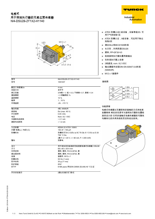
T 04:43:35+02:00型号NI4-DSU26-2Y1X2-H1140货号1051007额定工作距离Sn 4 mm 安装方式非齐平修正系数37#钢 = 1; 铝 = 0.3; 不锈钢= 0.7; 黄铜 = 0.4重复精度ð 2 满量程的 %温度漂移10 %磁滞1…10 %环境温度-25…+70 °C 输出性能4线, NAMUR 阀控制Exi (max. 45 V)开关频率0.05 kHz电压Nom. 8.2 VDC 无激励电流损耗ï 2.1 mA 激励电流损耗ð 1.2 mA认证依据KEMA 02 ATEX 1090X 内置 电感(L ) / 电容 (C )150 nF / 150 µH防爆标志防爆标识为II 2 G/Ex ia IIC T6 Gb /II 1 D Ex ia D 20T95 °C Da(最大 U = 20 V, I = 60 mA, P = 200 mW)警告防静电设计用于阀位回讯检测的双检测面电感式传感器, DSU26尺寸68 x 60 x 35.4 mm外壳材料塑料, 塑料, PA12-GF20, 黄感应面材料塑料, 塑料, PA12-GF20, 黑连接接插件, M12 x 1防震动性55 Hz (1 mm)防冲击性30 g (11 ms)防护等级IP67MTTF 6198 years 符合SN 29500 (Ed.99) 40 °C认证开关状态指示2路LED指示灯 黄/红sATEX 防爆认证II 组设备,设备等级2G. 可用于气体危险1区sATEX 防爆认证,II组设备,可应用于粉尘危险0区s 满足SIL2和IEC61508标准s 长方形,外壳类型DSU26s 塑料, PP -GF30-V0s 检测旋转执行器位置两路输出s 在标准执行器上安装s 2线直流, nom. 8.2 VDCs输出遵循本安型DIN EN 60947-5-6标准(NAMUR)sM12 x 1接插件接线图功能原理电感式传感器以无磨损和非接触的方式来检测金属物体 阀位回讯是专为旋转执行器的位置检测而设计的 它将非接触式电感传感器的可靠性与模块化的外壳系统的灵活性结合起来。
MAX487ESA中文资料
For pricing, delivery, and ordering information,please contact Maxim/Dallas Direct!at 1-888-629-4642, or visit Maxim’s website at .General DescriptionThe MAX481, MAX483, MAX485, MAX487–MAX491, and MAX1487 are low-power transceivers for RS-485 and RS-422 communication. Each part contains one driver and one receiver. The MAX483, MAX487, MAX488, and MAX489feature reduced slew-rate drivers that minimize EMI and reduce reflections caused by improperly terminated cables,thus allowing error-free data transmission up to 250kbps.The driver slew rates of the MAX481, MAX485, MAX490,MAX491, and MAX1487 are not limited, allowing them to transmit up to 2.5Mbps.These transceivers draw between 120µA and 500µA of supply current when unloaded or fully loaded with disabled drivers. Additionally, the MAX481, MAX483, and MAX487have a low-current shutdown mode in which they consume only 0.1µA. All parts operate from a single 5V supply.Drivers are short-circuit current limited and are protected against excessive power dissipation by thermal shutdown circuitry that places the driver outputs into a high-imped-ance state. The receiver input has a fail-safe feature that guarantees a logic-high output if the input is open circuit.The MAX487 and MAX1487 feature quarter-unit-load receiver input impedance, allowing up to 128 MAX487/MAX1487 transceivers on the bus. Full-duplex communi-cations are obtained using the MAX488–MAX491, while the MAX481, MAX483, MAX485, MAX487, and MAX1487are designed for half-duplex applications.________________________ApplicationsLow-Power RS-485 Transceivers Low-Power RS-422 Transceivers Level TranslatorsTransceivers for EMI-Sensitive Applications Industrial-Control Local Area Networks__Next Generation Device Features♦For Fault-Tolerant ApplicationsMAX3430: ±80V Fault-Protected, Fail-Safe, 1/4Unit Load, +3.3V, RS-485 TransceiverMAX3440E–MAX3444E: ±15kV ESD-Protected,±60V Fault-Protected, 10Mbps, Fail-Safe, RS-485/J1708 Transceivers♦For Space-Constrained ApplicationsMAX3460–MAX3464: +5V, Fail-Safe, 20Mbps,Profibus RS-485/RS-422 TransceiversMAX3362: +3.3V, High-Speed, RS-485/RS-422Transceiver in a SOT23 PackageMAX3280E–MAX3284E: ±15kV ESD-Protected,52Mbps, +3V to +5.5V, SOT23, RS-485/RS-422,True Fail-Safe ReceiversMAX3293/MAX3294/MAX3295: 20Mbps, +3.3V,SOT23, RS-855/RS-422 Transmitters ♦For Multiple Transceiver ApplicationsMAX3030E–MAX3033E: ±15kV ESD-Protected,+3.3V, Quad RS-422 Transmitters ♦For Fail-Safe ApplicationsMAX3080–MAX3089: Fail-Safe, High-Speed (10Mbps), Slew-Rate-Limited RS-485/RS-422Transceivers♦For Low-Voltage ApplicationsMAX3483E/MAX3485E/MAX3486E/MAX3488E/MAX3490E/MAX3491E: +3.3V Powered, ±15kV ESD-Protected, 12Mbps, Slew-Rate-Limited,True RS-485/RS-422 TransceiversMAX481/MAX483/MAX485/MAX487–MAX491/MAX1487Low-Power, Slew-Rate-Limited RS-485/RS-422 Transceivers______________________________________________________________Selection Table19-0122; Rev 8; 10/03Ordering Information appears at end of data sheet.M A X 481/M A X 483/M A X 485/M A X 487–M A X 491/M A X 1487Low-Power, Slew-Rate-Limited RS-485/RS-422 Transceivers 2_______________________________________________________________________________________ABSOLUTE MAXIMUM RATINGSSupply Voltage (V CC ).............................................................12V Control Input Voltage (RE , DE)...................-0.5V to (V CC + 0.5V)Driver Input Voltage (DI).............................-0.5V to (V CC + 0.5V)Driver Output Voltage (A, B)...................................-8V to +12.5V Receiver Input Voltage (A, B).................................-8V to +12.5V Receiver Output Voltage (RO).....................-0.5V to (V CC +0.5V)Continuous Power Dissipation (T A = +70°C)8-Pin Plastic DIP (derate 9.09mW/°C above +70°C)....727mW 14-Pin Plastic DIP (derate 10.00mW/°C above +70°C)..800mW 8-Pin SO (derate 5.88mW/°C above +70°C).................471mW14-Pin SO (derate 8.33mW/°C above +70°C)...............667mW 8-Pin µMAX (derate 4.1mW/°C above +70°C)..............830mW 8-Pin CERDIP (derate 8.00mW/°C above +70°C).........640mW 14-Pin CERDIP (derate 9.09mW/°C above +70°C).......727mW Operating Temperature RangesMAX4_ _C_ _/MAX1487C_ A...............................0°C to +70°C MAX4__E_ _/MAX1487E_ A.............................-40°C to +85°C MAX4__MJ_/MAX1487MJA...........................-55°C to +125°C Storage Temperature Range.............................-65°C to +160°C Lead Temperature (soldering, 10sec).............................+300°CDC ELECTRICAL CHARACTERISTICS(V CC = 5V ±5%, T A = T MIN to T MAX , unless otherwise noted.) (Notes 1, 2)Stresses beyond those listed under “Absolute Maximum Ratings” may cause permanent damage to the device. These are stress ratings only, and functional operation of the device at these or any other conditions beyond those indicated in the operational sections of the specifications is not implied. Exposure to absolute maximum rating conditions for extended periods may affect device reliability.V V IN = -7VV IN = 12V V IN = -7V V IN = 12V Input Current (A, B)I IN2V TH k Ω48-7V ≤V CM ≤12V, MAX487/MAX1487R INReceiver Input Resistance -7V ≤V CM ≤12V, all devices except MAX487/MAX1487R = 27Ω(RS-485), Figure 40.4V ≤V O ≤2.4VR = 50Ω(RS-422)I O = 4mA, V ID = -200mV I O = -4mA, V ID = 200mV V CM = 0V-7V ≤V CM ≤12V DE, DI, RE DE, DI, RE MAX487/MAX1487,DE = 0V, V CC = 0V or 5.25VDE, DI, RE R = 27Ωor 50Ω, Figure 4R = 27Ωor 50Ω, Figure 4R = 27Ωor 50Ω, Figure 4DE = 0V;V CC = 0V or 5.25V,all devices except MAX487/MAX1487CONDITIONSk Ω12µA ±1I OZRThree-State (high impedance)Output Current at ReceiverV 0.4V OL Receiver Output Low Voltage 3.5V OH Receiver Output High Voltage mV 70∆V TH Receiver Input Hysteresis V -0.20.2Receiver Differential Threshold Voltage-0.2mA 0.25mA-0.81.01.55V OD2Differential Driver Output (with load)V 2V 5V OD1Differential Driver Output (no load)µA±2I IN1Input CurrentV 0.8V IL Input Low Voltage V 2.0V IH Input High Voltage V 0.2∆V OD Change in Magnitude of Driver Common-Mode Output Voltage for Complementary Output States V 0.2∆V OD Change in Magnitude of Driver Differential Output Voltage for Complementary Output States V 3V OC Driver Common-Mode Output VoltageUNITS MINTYPMAX SYMBOL PARAMETERMAX481/MAX483/MAX485/MAX487–MAX491/MAX1487Low-Power, Slew-Rate-Limited RS-485/RS-422 Transceivers_______________________________________________________________________________________3SWITCHING CHARACTERISTICS—MAX481/MAX485, MAX490/MAX491, MAX1487(V CC = 5V ±5%, T A = T MIN to T MAX , unless otherwise noted.) (Notes 1, 2)DC ELECTRICAL CHARACTERISTICS (continued)(V CC = 5V ±5%, T A = T MIN to T MAX , unless otherwise noted.) (Notes 1, 2)ns 103060t PHLDriver Rise or Fall Time Figures 6 and 8, R DIFF = 54Ω, C L1= C L2= 100pF ns MAX490M, MAX491M MAX490C/E, MAX491C/E2090150MAX481, MAX485, MAX1487MAX490M, MAX491MMAX490C/E, MAX491C/E MAX481, MAX485, MAX1487Figures 6 and 8, R DIFF = 54Ω,C L1= C L2= 100pF MAX481 (Note 5)Figures 5 and 11, C RL = 15pF, S2 closedFigures 5 and 11, C RL = 15pF, S1 closed Figures 5 and 11, C RL = 15pF, S2 closed Figures 5 and 11, C RL = 15pF, S1 closed Figures 6 and 10, R DIFF = 54Ω,C L1= C L2= 100pFFigures 6 and 8,R DIFF = 54Ω,C L1= C L2= 100pF Figures 6 and 10,R DIFF = 54Ω,C L1= C L2= 100pF CONDITIONS ns 510t SKEW ns50200600t SHDNTime to ShutdownMbps 2.5f MAX Maximum Data Rate ns 2050t HZ Receiver Disable Time from High ns 103060t PLH 2050t LZ Receiver Disable Time from Low ns 2050t ZH Driver Input to Output Receiver Enable to Output High ns 2050t ZL Receiver Enable to Output Low 2090200ns ns 134070t HZ t SKD Driver Disable Time from High |t PLH - t PHL |DifferentialReceiver Skewns 4070t LZ Driver Disable Time from Low ns 4070t ZL Driver Enable to Output Low 31540ns51525ns 31540t R , t F 2090200Driver Output Skew to Output t PLH , t PHL Receiver Input to Output4070t ZH Driver Enable to Output High UNITS MIN TYP MAX SYMBOL PARAMETERFigures 7 and 9, C L = 100pF, S2 closed Figures 7 and 9, C L = 100pF, S1 closed Figures 7 and 9, C L = 15pF, S1 closed Figures 7 and 9, C L = 15pF, S2 closedM A X 481/M A X 483/M A X 485/M A X 487–M A X 491/M A X 1487Low-Power, Slew-Rate-Limited RS-485/RS-422 Transceivers 4_______________________________________________________________________________________SWITCHING CHARACTERISTICS—MAX483, MAX487/MAX488/MAX489(V CC = 5V ±5%, T A = T MIN to T MAX , unless otherwise noted.) (Notes 1, 2)SWITCHING CHARACTERISTICS—MAX481/MAX485, MAX490/MAX491, MAX1487 (continued)(V CC = 5V ±5%, T A = T MIN to T MAX , unless otherwise noted.) (Notes 1, 2)3001000Figures 7 and 9, C L = 100pF, S2 closed Figures 7 and 9, C L = 100pF, S1 closed Figures 5 and 11, C L = 15pF, S2 closed,A - B = 2VCONDITIONSns 40100t ZH(SHDN)Driver Enable from Shutdown toOutput High (MAX481)nsFigures 5 and 11, C L = 15pF, S1 closed,B - A = 2Vt ZL(SHDN)Receiver Enable from Shutdownto Output Low (MAX481)ns 40100t ZL(SHDN)Driver Enable from Shutdown toOutput Low (MAX481)ns 3001000t ZH(SHDN)Receiver Enable from Shutdownto Output High (MAX481)UNITS MINTYP MAX SYMBOLPARAMETERt PLH t SKEW Figures 6 and 8, R DIFF = 54Ω,C L1= C L2= 100pFt PHL Figures 6 and 8, R DIFF = 54Ω,C L1= C L2= 100pFDriver Input to Output Driver Output Skew to Output ns 100800ns ns 2000MAX483/MAX487, Figures 7 and 9,C L = 100pF, S2 closedt ZH(SHDN)Driver Enable from Shutdown to Output High2502000ns2500MAX483/MAX487, Figures 5 and 11,C L = 15pF, S1 closedt ZL(SHDN)Receiver Enable from Shutdown to Output Lowns 2500MAX483/MAX487, Figures 5 and 11,C L = 15pF, S2 closedt ZH(SHDN)Receiver Enable from Shutdown to Output Highns 2000MAX483/MAX487, Figures 7 and 9,C L = 100pF, S1 closedt ZL(SHDN)Driver Enable from Shutdown to Output Lowns 50200600MAX483/MAX487 (Note 5) t SHDN Time to Shutdownt PHL t PLH , t PHL < 50% of data period Figures 5 and 11, C RL = 15pF, S2 closed Figures 5 and 11, C RL = 15pF, S1 closed Figures 5 and 11, C RL = 15pF, S2 closed Figures 5 and 11, C RL = 15pF, S1 closed Figures 7 and 9, C L = 15pF, S2 closed Figures 6 and 10, R DIFF = 54Ω,C L1= C L2= 100pFFigures 7 and 9, C L = 15pF, S1 closed Figures 7 and 9, C L = 100pF, S1 closed Figures 7 and 9, C L = 100pF, S2 closed CONDITIONSkbps 250f MAX 2508002000Maximum Data Rate ns 2050t HZ Receiver Disable Time from High ns 25080020002050t LZ Receiver Disable Time from Low ns 2050t ZH Receiver Enable to Output High ns 2050t ZL Receiver Enable to Output Low ns ns 1003003000t HZ t SKD Driver Disable Time from High I t PLH - t PHL I DifferentialReceiver SkewFigures 6 and 10, R DIFF = 54Ω,C L1= C L2= 100pFns 3003000t LZ Driver Disable Time from Low ns 2502000t ZL Driver Enable to Output Low ns Figures 6 and 8, R DIFF = 54Ω,C L1= C L2= 100pFns 2502000t R , t F 2502000Driver Rise or Fall Time ns t PLH Receiver Input to Output2502000t ZH Driver Enable to Output High UNITS MIN TYP MAX SYMBOL PARAMETERMAX481/MAX483/MAX485/MAX487–MAX491/MAX1487Low-Power, Slew-Rate-Limited RS-485/RS-422 Transceivers_______________________________________________________________________________________530002.5OUTPUT CURRENT vs.RECEIVER OUTPUT LOW VOLTAGE525M A X 481-01OUTPUT LOW VOLTAGE (V)O U T P U T C U R R E N T (m A )1.515100.51.02.0203540450.90.1-50-252575RECEIVER OUTPUT LOW VOLTAGE vs.TEMPERATURE0.30.7TEMPERATURE (°C)O U T P U TL O W V O L T A G E (V )500.50.80.20.60.40100125-20-41.5 2.0 3.0 5.0OUTPUT CURRENT vs.RECEIVER OUTPUT HIGH VOLTAGE-8-16M A X 481-02OUTPUT HIGH VOLTAGE (V)O U T P U T C U R R E N T (m A )2.5 4.0-12-18-6-14-10-203.54.5 4.83.2-50-252575RECEIVER OUTPUT HIGH VOLTAGE vs.TEMPERATURE3.64.4TEMPERATURE (°C)O U T P UT H I G H V O L T A G E (V )0504.04.63.44.23.83.01001259000 1.0 3.0 4.5DRIVER OUTPUT CURRENT vs.DIFFERENTIAL OUTPUT VOLTAGE1070M A X 481-05DIFFERENTIAL OUTPUT VOLTAGE (V)O U T P U T C U R R E N T (m A )2.0 4.05030806040200.5 1.5 2.53.5 2.31.5-50-2525125DRIVER DIFFERENTIAL OUTPUT VOLTAGEvs. TEMPERATURE1.72.1TEMPERATURE (°C)D I F FE R E N T I A L O U T P U T V O L T A G E (V )751.92.21.62.01.8100502.4__________________________________________Typical Operating Characteristics(V CC = 5V, T A = +25°C, unless otherwise noted.)NOTES FOR ELECTRICAL/SWITCHING CHARACTERISTICSNote 1:All currents into device pins are positive; all currents out of device pins are negative. All voltages are referenced to deviceground unless otherwise specified.Note 2:All typical specifications are given for V CC = 5V and T A = +25°C.Note 3:Supply current specification is valid for loaded transmitters when DE = 0V.Note 4:Applies to peak current. See Typical Operating Characteristics.Note 5:The MAX481/MAX483/MAX487 are put into shutdown by bringing RE high and DE low. If the inputs are in this state for lessthan 50ns, the parts are guaranteed not to enter shutdown. If the inputs are in this state for at least 600ns, the parts are guaranteed to have entered shutdown. See Low-Power Shutdown Mode section.M A X 481/M A X 483/M A X 485/M A X 487–M A X 491/M A X 1487Low-Power, Slew-Rate-Limited RS-485/RS-422 Transceivers 6___________________________________________________________________________________________________________________Typical Operating Characteristics (continued)(V CC = 5V, T A = +25°C, unless otherwise noted.)120008OUTPUT CURRENT vs.DRIVER OUTPUT LOW VOLTAGE20100M A X 481-07OUTPUT LOW VOLTAGE (V)O U T P U T C U R R E N T (m A )6604024801012140-1200-7-5-15OUTPUT CURRENT vs.DRIVER OUTPUT HIGH VOLTAGE-20-80M A X 481-08OUTPUT HIGH VOLTAGE (V)O U T P U T C U R R E N T (m A )-31-603-6-4-2024-100-40100-40-60-2040100120MAX1487SUPPLY CURRENT vs. TEMPERATURE300TEMPERATURE (°C)S U P P L Y C U R R E N T (µA )20608050020060040000140100-50-2550100MAX481/MAX485/MAX490/MAX491SUPPLY CURRENT vs. TEMPERATURE300TEMPERATURE (°C)S U P P L Y C U R R E N T (µA )257550020060040000125100-50-2550100MAX483/MAX487–MAX489SUPPLY CURRENT vs. TEMPERATURE300TEMPERATURE (°C)S U P P L Y C U R R E N T (µA )257550020060040000125MAX481/MAX483/MAX485/MAX487–MAX491/MAX1487Low-Power, Slew-Rate-Limited RS-485/RS-422 Transceivers_______________________________________________________________________________________7______________________________________________________________Pin DescriptionFigure 1. MAX481/MAX483/MAX485/MAX487/MAX1487 Pin Configuration and Typical Operating CircuitM A X 481/M A X 483/M A X 485/M A X 487–M A X 491/M A X 1487__________Applications InformationThe MAX481/MAX483/MAX485/MAX487–MAX491 and MAX1487 are low-power transceivers for RS-485 and RS-422 communications. The MAX481, MAX485, MAX490,MAX491, and MAX1487 can transmit and receive at data rates up to 2.5Mbps, while the MAX483, MAX487,MAX488, and MAX489 are specified for data rates up to 250kbps. The MAX488–MAX491 are full-duplex trans-ceivers while the MAX481, MAX483, MAX485, MAX487,and MAX1487 are half-duplex. In addition, Driver Enable (DE) and Receiver Enable (RE) pins are included on the MAX481, MAX483, MAX485, MAX487, MAX489,MAX491, and MAX1487. When disabled, the driver and receiver outputs are high impedance.MAX487/MAX1487:128 Transceivers on the BusThe 48k Ω, 1/4-unit-load receiver input impedance of the MAX487 and MAX1487 allows up to 128 transceivers on a bus, compared to the 1-unit load (12k Ωinput impedance) of standard RS-485 drivers (32 trans-ceivers maximum). Any combination of MAX487/MAX1487 and other RS-485 transceivers with a total of 32 unit loads or less can be put on the bus. The MAX481/MAX483/MAX485 and MAX488–MAX491 have standard 12k ΩReceiver Input impedance.Low-Power, Slew-Rate-Limited RS-485/RS-422 Transceivers 8_______________________________________________________________________________________Figure 2. MAX488/MAX490 Pin Configuration and Typical Operating CircuitFigure 3. MAX489/MAX491 Pin Configuration and Typical Operating CircuitMAX483/MAX487/MAX488/MAX489:Reduced EMI and ReflectionsThe MAX483 and MAX487–MAX489 are slew-rate limit-ed, minimizing EMI and reducing reflections caused by improperly terminated cables. Figure 12 shows the dri-ver output waveform and its Fourier analysis of a 150kHz signal transmitted by a MAX481, MAX485,MAX490, MAX491, or MAX1487. High-frequency har-monics with large amplitudes are evident. Figure 13shows the same information displayed for a MAX483,MAX487, MAX488, or MAX489 transmitting under the same conditions. Figure 13’s high-frequency harmonics have much lower amplitudes, and the potential for EMI is significantly reduced.MAX481/MAX483/MAX485/MAX487–MAX491/MAX1487Low-Power, Slew-Rate-Limited RS-485/RS-422 Transceivers_______________________________________________________________________________________9_________________________________________________________________Test CircuitsFigure 4. Driver DC Test Load Figure 5. Receiver Timing Test LoadFigure 6. Driver/Receiver Timing Test Circuit Figure 7. Driver Timing Test LoadM A X 481/M A X 483/M A X 485/M A X 487–M A X 491/M A X 1487Low-Power, Slew-Rate-Limited RS-485/RS-422 Transceivers 10_______________________________________________________Switching Waveforms_________________Function Tables (MAX481/MAX483/MAX485/MAX487/MAX1487)Figure 8. Driver Propagation DelaysFigure 9. Driver Enable and Disable Times (except MAX488 and MAX490)Figure 10. Receiver Propagation DelaysFigure 11. Receiver Enable and Disable Times (except MAX488and MAX490)Table 1. TransmittingTable 2. ReceivingLow-Power Shutdown Mode (MAX481/MAX483/MAX487)A low-power shutdown mode is initiated by bringing both RE high and DE low. The devices will not shut down unless both the driver and receiver are disabled.In shutdown, the devices typically draw only 0.1µA of supply current.RE and DE may be driven simultaneously; the parts are guaranteed not to enter shutdown if RE is high and DE is low for less than 50ns. If the inputs are in this state for at least 600ns, the parts are guaranteed to enter shutdown.For the MAX481, MAX483, and MAX487, the t ZH and t ZL enable times assume the part was not in the low-power shutdown state (the MAX485/MAX488–MAX491and MAX1487 can not be shut down). The t ZH(SHDN)and t ZL(SHDN)enable times assume the parts were shut down (see Electrical Characteristics ).It takes the drivers and receivers longer to become enabled from the low-power shutdown state (t ZH(SHDN ), t ZL(SHDN)) than from the operating mode (t ZH , t ZL ). (The parts are in operating mode if the –R —E –,DE inputs equal a logical 0,1 or 1,1 or 0, 0.)Driver Output ProtectionExcessive output current and power dissipation caused by faults or by bus contention are prevented by two mechanisms. A foldback current limit on the output stage provides immediate protection against short cir-cuits over the whole common-mode voltage range (see Typical Operating Characteristics ). In addition, a ther-mal shutdown circuit forces the driver outputs into a high-impedance state if the die temperature rises excessively.Propagation DelayMany digital encoding schemes depend on the differ-ence between the driver and receiver propagation delay times. Typical propagation delays are shown in Figures 15–18 using Figure 14’s test circuit.The difference in receiver delay times, | t PLH - t PHL |, is typically under 13ns for the MAX481, MAX485,MAX490, MAX491, and MAX1487 and is typically less than 100ns for the MAX483 and MAX487–MAX489.The driver skew times are typically 5ns (10ns max) for the MAX481, MAX485, MAX490, MAX491, and MAX1487, and are typically 100ns (800ns max) for the MAX483 and MAX487–MAX489.MAX481/MAX483/MAX485/MAX487–MAX491/MAX1487Low-Power, Slew-Rate-Limited RS-485/RS-422 Transceivers______________________________________________________________________________________1110dB/div0Hz5MHz500kHz/div10dB/div0Hz5MHz500kHz/divFigure 12. Driver Output Waveform and FFT Plot of MAX481/MAX485/MAX490/MAX491/MAX1487 Transmitting a 150kHz SignalFigure 13. Driver Output Waveform and FFT Plot of MAX483/MAX487–MAX489 Transmitting a 150kHz SignalM A X 481/M A X 483/M A X 485/M A X 487–M A X 491/M A X 1487Low-Power, Slew-Rate-Limited RS-485/RS-422 Transceivers 12______________________________________________________________________________________V CC = 5V T A = +25°CV CC = 5V T A = +25°CV CC = 5V T A = +25°CV CC = 5V T A = +25°CFigure 14. Receiver Propagation Delay Test CircuitFigure 15. MAX481/MAX485/MAX490/MAX491/MAX1487Receiver t PHLFigure 16. MAX481/MAX485/MAX490/MAX491/MAX1487Receiver t PLHPHL Figure 18. MAX483, MAX487–MAX489 Receiver t PLHLine Length vs. Data RateThe RS-485/RS-422 standard covers line lengths up to 4000 feet. For line lengths greater than 4000 feet, see Figure 23.Figures 19 and 20 show the system differential voltage for the parts driving 4000 feet of 26AWG twisted-pair wire at 110kHz into 120Ωloads.Typical ApplicationsThe MAX481, MAX483, MAX485, MAX487–MAX491, and MAX1487 transceivers are designed for bidirectional data communications on multipoint bus transmission lines.Figures 21 and 22 show typical network applications circuits. These parts can also be used as line repeaters, with cable lengths longer than 4000 feet, as shown in Figure 23.To minimize reflections, the line should be terminated at both ends in its characteristic impedance, and stub lengths off the main line should be kept as short as possi-ble. The slew-rate-limited MAX483 and MAX487–MAX489are more tolerant of imperfect termination.MAX481/MAX483/MAX485/MAX487–MAX491/MAX1487Low-Power, Slew-Rate-Limited RS-485/RS-422 Transceivers______________________________________________________________________________________13DIV Y -V ZRO5V 0V1V0V -1V5V 0V2µs/divFigure 19. MAX481/MAX485/MAX490/MAX491/MAX1487 System Differential Voltage at 110kHz Driving 4000ft of Cable Figure 20. MAX483, MAX487–MAX489 System Differential Voltage at 110kHz Driving 4000ft of CableFigure 21. MAX481/MAX483/MAX485/MAX487/MAX1487 Typical Half-Duplex RS-485 NetworkM A X 481/M A X 483/M A X 485/M A X 487–M A X 491/M A X 1487Low-Power, Slew-Rate-Limited RS-485/RS-422 Transceivers 14______________________________________________________________________________________Figure 22. MAX488–MAX491 Full-Duplex RS-485 NetworkFigure 23. Line Repeater for MAX488–MAX491Isolated RS-485For isolated RS-485 applications, see the MAX253 and MAX1480 data sheets.MAX481/MAX483/MAX485/MAX487–MAX491/MAX1487Low-Power, Slew-Rate-Limited RS-485/RS-422 Transceivers______________________________________________________________________________________15_______________Ordering Information_________________Chip TopographiesMAX481/MAX483/MAX485/MAX487/MAX1487N.C. RO 0.054"(1.372mm)0.080"(2.032mm)DE DIGND B N.C.V CCARE * Contact factory for dice specifications.__Ordering Information (continued)M A X 481/M A X 483/M A X 485/M A X 487–M A X 491/M A X 1487Low-Power, Slew-Rate-Limited RS-485/RS-422 Transceivers 16______________________________________________________________________________________TRANSISTOR COUNT: 248SUBSTRATE CONNECTED TO GNDMAX488/MAX490B RO 0.054"(1.372mm)0.080"(2.032mm)N.C. DIGND Z A V CCYN.C._____________________________________________Chip Topographies (continued)MAX489/MAX491B RO 0.054"(1.372mm)0.080"(2.032mm)DE DIGND Z A V CCYREMAX481/MAX483/MAX485/MAX487–MAX491/MAX1487Low-Power, Slew-Rate-Limited RS-485/RS-422 Transceivers______________________________________________________________________________________17Package Information(The package drawing(s) in this data sheet may not reflect the most current specifications. For the latest package outline information go to /packages .)S O I C N .E P SM A X 481/M A X 483/M A X 485/M A X 487–M A X 491/M A X 1487Low-Power, Slew-Rate-Limited RS-485/RS-422 Transceivers 18______________________________________________________________________________________Package Information (continued)(The package drawing(s) in this data sheet may not reflect the most current specifications. For the latest package outline information go to /packages .)MAX481/MAX483/MAX485/MAX487–MAX491Low-Power, Slew-Rate-Limited RS-485/RS-422 TransceiversMaxim cannot assume responsibility for use of any circuitry other than circuitry entirely embodied in a Maxim product. No circuit patent licenses are implied. Maxim reserves the right to change the circuitry and specifications without notice at any time.Maxim Integrated Products, 120 San Gabriel Drive, Sunnyvale, CA 94086 408-737-7600 ____________________19©2003 Maxim Integrated ProductsPrinted USAis a registered trademark of Maxim Integrated Products.M A X 481/M A X 483/M A X 485/M A X 487–M A X 491/M A X 1487P D I P N .E PSPackage Information (continued)(The package drawing(s) in this data sheet may not reflect the most current specifications. For the latest package outline information go to /packages .)。
四代站用户使用手册硬件部分PPT学习教案

4、Master Cloc k Gen erator MCLG 主时 钟发生 器
MCLG为BTS生 成精确 的时钟 ,由该 基准还 衍生出 其他时 钟信号 ,并分 配给其 它单元 。
第10页/共46页
第11页/共46页
(六) DUAL BASEBAND
Unit (BB2x)基带单元
处理控制来表明BOIx 单元的状态.
2、Field Progra mma ble Gate Arra y 现场 可编程 门阵列
FPGA 具 有下列 功能:
监测控制 BTS的 风扇状 态
检查外部 帧时钟
允许由TS xx和BB2x之 间的软 件所形 成的多 种连接
第9页/共46页
3、D-BUS D总 线
Wideband Combiner
Air flow
Duplexer unit
BottomRF filter Unit Cooling Fan
第23页/共46页
99625895
(十)Du al Variable Gain Duplex Filter Unit
(DVxx) 对偶变 量增益 双工滤 波器单 元
第33页/共46页
(二) COMBI NING BY-PASS 直 接合路
TRX RF Units
Receive Multicoupler
Dual Duplex Unit
Antennas
TX
RX
main
div
LNA
Duplexer Duplexer
TX
RX
main
div
Splitte r
Splitte r
Red – Unit Faulty or No BB2 Connection Yellow – Unit On, Working, and not Transmitting (TX Off) Green – Unit On and Working Blinking Red – Loop Test
CM44中文技术资料
通信和数据处理 . . . . . . . . . . . . . . . . . . . . . . . . . . . . . . .14 可靠性 . . . . . . . . . . . . . . . . . . . . . . . . . . . . . . . . . . . . . . .14
通信规范参数 . . . . . . . . . . . . . . . . . . . . . . . . . . . . . . . . .23
HART . . . . . . . . . . . . . . . . . . . . . . . . . . . . . . . . . . . . . . . . . . . . . . PROFIBUS DP . . . . . . . . . . . . . . . . . . . . . . . . . . . . . . . . . . . . . . . Modbus RS485 . . . . . . . . . . . . . . . . . . . . . . . . . . . . . . . . . . . . . Modbus TCP . . . . . . . . . . . . . . . . . . . . . . . . . . . . . . . . . . . . . . . . Web 服务器 . . . . . . . . . . . . . . . . . . . . . . . . . . . . . . . . . . . . . . . . 23 23 23 24 24
有源电流输出 . . . . . . . . . . . . . . . . . . . . . . . . . . . . . . . . .21
AO4474

Symbol V DS V GSI DM I AR E AR T J , T STG SymbolTyp Max 28345771R θJL1623Junction and Storage Temperature Range °C-55 to 1503.7W T A =70°C 2.4Power Dissipation T A =25°C PD MaximumUnits Parameter 30°C/W Absolute Maximum Ratings T A =25°C unless otherwise noted V V ±12Gate-Source Voltage Drain-Source Voltage Maximum Junction-to-Ambient A Steady-State Maximum Junction-to-Lead CSteady-State°C/WThermal CharacteristicsParameterUnits Maximum Junction-to-Ambient A t ≤ 10sR θJA °C/W Repetitive avalanche energy 0.1mH B, G 88mJ Pulsed Drain Current B60AAvalanche Current B, G42A T A =70°C10.7Continuous Drain Current A, FT A =25°C I DSM 13.4 100% UIS Tested 100% Rg TestedSOIC-8Top View Bottom View D DD D SS S G GDSSymbolMin TypMaxUnits BV DSS 30V 1T J =55°C5I GSS 0.1µA V GS(th)1 1.552.5V I D(ON)60A 9.511.5T J =125°C16.2181113.5m Ωg FS 40S VSD 0.741.0V I S5A C iss 12101452pF C oss 330396pF C rss 85119pF R g0.81.2 1.6ΩQ g (10V)2228nC Q g (4.5V)1013nC Q gs 3.7nC Q gd 2.7nC t D(on)10ns t r 6.3ns t D(off)21ns t f 2.8ns t rr 3645ns Q rr 47nC t rr 2027ns Q rr55nCTHIS PRODUCT HAS BEEN DESIGNED AND QUALIFIED FOR THE CONSUMER MARKET. APPLICATIONS OR USES AS CRITICAL COMPONENTS IN LIFE SUPPORT DEVICES OR SYSTEMS ARE NOT AUTHORIZED. AOS DOES NOT ASSUME ANY LIABILITY ARISING OUT OF SUCH APPLICATIONS OR USES OF ITS PRODUCTS. AOS RESERVES THE RIGHT TO IMPROVE PRODUCT DESIGN,FUNCTIONS AND RELIABILITY WITHOUT NOTICE.Body Diode Reverse Recovery TimeI F =13.4A, dI/dt=100A/µsBody Diode Reverse Recovery Charge I F =13.4A, dI/dt=100A/µsGate Drain Charge V GS =0V, V DS =15V, f=1MHz SWITCHING PARAMETERS Total Gate Charge Gate Source Charge Gate resistanceV GS =0V, V DS =0V, f=1MHzTotal Gate Charge V GS =10V, V DS =15V, I D =13.4ATurn-On Rise Time Turn-Off DelayTime V GS =10V, V DS =15V, R L =1.1Ω,R GEN =3ΩTurn-Off Fall TimeTurn-On DelayTime m ΩV GS =4.5V, I D =10AI S =1A,V GS =0VV DS =5V, I D =13.4A Maximum Body-Diode Continuous CurrentInput Capacitance Output CapacitanceDYNAMIC PARAMETERS R DS(ON)Static Drain-Source On-ResistanceForward Transconductance Diode Forward VoltageI DSS µA Gate Threshold Voltage V DS =V GS I D =250µA V DS =30V, V GS =0VV DS =0V, V GS = ±12V Zero Gate Voltage Drain Current Gate-Body leakage current Electrical Characteristics (T J =25°C unless otherwise noted)STATIC PARAMETERS ParameterConditions Body Diode Reverse Recovery TimeBody Diode Reverse Recovery Charge I F =13.4A, dI/dt=500A/µsDrain-Source Breakdown Voltage On state drain currentI D =250µA, V GS =0V V GS =10V, V DS =5V V GS =10V, I D =13.4AReverse Transfer Capacitance I F =13.4A, dI/dt=500A/µs A: The value of R θJA is measured with the device mounted on 1in 2 FR-4 board with 2oz. Copper, in a still air environment withT A =25°C. The value in any given application depends on the user's specific board design.B: Repetitive rating, pulse width limited by junction temperature.C. The R θJA is the sum of the thermal impedence from junction to lead R θJL and lead to ambient.D. The static characteristics in Figures 1 to 6 are obtained using <300 µs pulses, duty cycle 0.5% max.E. These tests are performed with the device mounted on 1 in 2 FR-4 board with 2oz. Copper, in a still air environment with T A =25°C. The SOA curve provides a single pulse rating.F. The current rating is based on the t ≤ 10s junction to ambient thermal resistance rating.G: L=100uH, V DD =0V, R G =0Ω, rated V DS =30V and V GS =10V Rev4: Nov. 2010TYPICAL ELECTRICAL AND THERMAL CHARACTERISTICS。
MAX4472中文资料
Features
o Ultra-Low 750nA Supply Current Per Amplifier o Ultra-Low +1.8V Supply Voltage Operatommon-Mode Range o Outputs Swing Rail-to-Rail o Outputs Source and Sink 11mA of Load Current o No Phase Reversal for Overdriven Inputs o High 120dB Open-Loop Voltage Gain o Low 500µV Input Offset Voltage o 9kHz Gain-Bandwidth Product
an447_AN 447_ Interfacing Cyclone III Devices with 3.3_3.0_2.5-V LVTTL_LVCMOS I_O Systems (PDF)

150n
The requirements on the absolute maximum DC input voltage and maximum allowed overshoot/undershoot voltage for Cyclone III and Cyclone IV devices might not be met if the signal integrity issues are not properly addressed when using Cyclone III and Cyclone IV devices in interfacing with 3.3/3.0/2.5-V LVTTL/LVCMOS systems. 1 You must design the I/O interfaces within the specifications recommended in “Design Guideline” to ensure device reliability and proper operation,
(4)
Notes to Table 1:
(1) This applies when the Cyclone III and Cyclone IV device I/O pin is assigned as input, bidirectional, or tristated output using the 3.3/3.0/2.5-V LVTTL/LVCMOS I/O standards. The Quartus II® software enables the PCI-clamp diode on this pin for each of these conditions by default. No attention is required when the Cyclone III and Cyclone IV device I/O pin is only used as output. (2) Other I/O standards do not require attention on the maximum input voltage, such as 1.8/1.5/1.2-V LVTTL/LVCMOS, 3.0-V PCI/PCI-X, voltage-referenced, and differential I/O standards. (3) The Cyclone III and Cyclone IV device I/O pin is over-driven by a higher external voltage. You must ensure that the DC current specification of the diode is met. For more information, refer to “PCI-Clamp Diode” on page 3. Alternatively, you can apply series termination to manage voltage overshoot. In such cases, Altera recommends that you disable the diode due to the possible presence of a high DC current. (4) Diode clamped voltage can still exceed the maximum DC and AC specifications due to the high VCCIO voltage level of the bank in which the I/O resides. You must manage the voltage overshoot. You can leave the diode enabled without concern for the DC current as the I/O pin is not over-driven.
- 1、下载文档前请自行甄别文档内容的完整性,平台不提供额外的编辑、内容补充、找答案等附加服务。
- 2、"仅部分预览"的文档,不可在线预览部分如存在完整性等问题,可反馈申请退款(可完整预览的文档不适用该条件!)。
- 3、如文档侵犯您的权益,请联系客服反馈,我们会尽快为您处理(人工客服工作时间:9:00-18:30)。
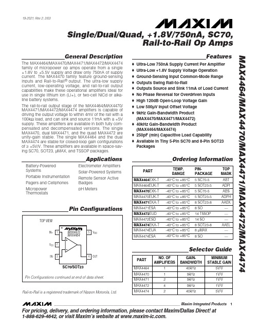
General DescriptionThe MAX4464/MAX4470/MAX4471/MAX4472/MAX4474family of micropower op amps operate from a single +1.8V to +5.5V supply and draw only 750nA of supply current. The MAX4470 family feature ground-sensing inputs and Rail-to-Rail ®output. The ultra-low supply current, low-operating voltage, and rail-to-rail output capabilities make these operational amplifiers ideal for use in single lithium ion (Li+), or two-cell NiCd or alka-line battery systems.The rail-to-rail output stage of the MAX4464/MAX4470/ MAX4471/MAX4472/MAX4474 amplifiers is capable of driving the output voltage to within 4mV of the rail with a 100k Ωload, and can sink and source 11mA with a +5V supply. These amplifiers are available in both fully com-pensated and decompensated versions. The single MAX4470, dual MAX4471, and the quad MAX4472 are unity-gain stable. The single MAX4464 and the dual MAX4474 are stable for closed-loop gain configurations of ≥+5V/V. These amplifiers are available in space-sav-ing SC70, SOT23, µMAX, and TSSOP packages.ApplicationsFeatureso Ultra-Low 750nA Supply Current Per Amplifier o Ultra-Low +1.8V Supply Voltage Operation o Ground-Sensing Input Common-Mode Range o Outputs Swing Rail-to-Railo Outputs Source and Sink 11mA of Load Current o No Phase Reversal for Overdriven Inputs o High 120dB Open-Loop Voltage Gain o Low 500µV Input Offset Voltage o 9kHz Gain-Bandwidth Product (MAX4470/MAX4471/MAX4472)o 40kHz Gain-Bandwidth Product (MAX4464/MAX4474)o 250pF (min) Capacitive Load Capability o Available in Tiny 5-Pin SC70 and 8-Pin SOT23PackagesMAX4464/MAX4470/MAX4471/MAX4472/MAX4474Single/Dual/Quad, +1.8V/750nA, SC70,Rail-to-Rail Op Amps________________________________________________________________Maxim Integrated Products 1Pin Configurations19-2021; Rev 2; 2/03For pricing, delivery, and ordering information,please contact Maxim/Dallas Direct!at 1-888-629-4642, or visit Maxim’s website at .Ordering InformationRail-to-Rail is a registered trademark of Nippon Motorola, Ltd.Selector GuideBattery-Powered SystemsPortable Instrumentation Pagers and Cellphones Micropower ThermostatsElectrometer Amplifiers Solar-Powered Systems Remote Sensor Active Badges pH MetersM A X 4464/M A X 4470/M A X 4471/M A X 4472/M A X 4474Single/Dual/Quad, +1.8V/750nA, SC70, Rail-to-Rail Op Amps 2_______________________________________________________________________________________ABSOLUTE MAXIMUM RATINGSELECTRICAL CHARACTERISTICSStresses beyond those listed under “Absolute Maximum Ratings” may cause permanent damage to the device. These are stress ratings only, and functional operation of the device at these or any other conditions beyond those indicated in the operational sections of the specifications is not implied. Exposure to absolute maximum rating conditions for extended periods may affect device reliability.V DD to V SS ...............................................................-0.3V to +6V IN_+ or IN_-......................................(V SS - 0.3V) to (V DD + 0.3V)OUT_ Shorted to V SS or V DD ......................................Continuous Continuous Power Dissipation (T A = +70°C)5-Pin SC70 (derate 3.1mW/°C above +70°C)...................247mW 5-Pin SOT23 (derate 7.1mW/°C above +70°C).................571mW 8-Pin SOT23 (derate 8.9mW/°C above +70°C).................714mW 8-Pin µMAX (derate 4.5mW/°C above +70°C)..................362mW8-Pin SO (derate 5.88mW/°C above +70°C)....................471mW 14-Pin TSSOP (derate 9.1mW/°C above +70°C)...........727mW 14-Pin SO (derate 8.33mW/°C above +70°C)...............667mW Operating Temperature Range .........................-40°C to +85°C Junction Temperature .....................................................+150°C Storage Temperature Range.............................-65°C to +150°C Lead Temperature (soldering, 10s) ................................+300°CMAX4464/MAX4470/MAX4471/MAX4472/MAX4474Single/Dual/Quad, +1.8V/750nA, SC70,Rail-to-Rail Op Amps_______________________________________________________________________________________3ELECTRICAL CHARACTERISTICS (continued)ELECTRICAL CHARACTERISTICSM A X 4464/M A X 4470/M A X 4471/M A X 4472/M A X 4474Single/Dual/Quad, +1.8V/750nA, SC70, Rail-to-Rail Op Amps 4_______________________________________________________________________________________Typical Operating Characteristics(V DD = +5V, V SS = 0, V CM = 0, R L = 100k Ωto V DD /2, T A = +25°C, unless otherwise noted.)0.20.10.50.40.30.70.80.60.91.5 3.0 3.52.0 2.5 4.0 4.5 5.0 5.5 6.0SUPPLY CURRENT PER AMPLIFIER vs.SUPPLY VOLTAGEM A X 4470–74 t o c 01SUPPLY VOLTAGE (V)S U P P L Y C U R R E N T (µA )0.20.10.50.40.30.70.80.60.9-500-25255075100SUPPLY CURRENT PER AMPLIFIER vs.TEMPERATUREM A X 4470–74 t o c 02TEMPERATURE (°C)S U P P L Y C U R R E N T (µA )00.100.050.300.200.250.150.400.450.350.50-50-25255075100OFFSET VOLTAGE vs.TEMPERATUREM A X 4470–74 t o c 03TEMPERATURE (°C)O F F S E T V O L T A G E (m V )00.100.050.200.150.300.250.350.450.400.501.01.50.52.02.53.03.54.0OFFSET VOLTAGEvs. COMMON-MODE VOLTAGEM A X 4470-74 t o c 04COMMON-MODE VOLTAGE (V)O F F S E T V O L T A G E (m V )-400-350-150-250-200-300-50-1000-50-25255075100INPUT BIAS CURRENT vs.TEMPERATUREM A X 4470–74 t o c 05TEMPERATURE (°C)I N P U T B I A S C U R R E N T (p A )-90-70-80-40-50-60-20-10-3000 1.51.00.5 2.0 2.5 3.0 3.5 4.0INPUT BIAS CURRENT MON-MODE VOLTAGEM A X 4470–74 t o c 06COMMON-MODE VOLTAGE (V)I N P U T B I A S C U R R E N T (p A )0-1001010010k1kPOWER-SUPPLY REJECTION RATIO vs.FREQUENCY-80-90M A X 4470–74 t o c 07FREQUENCY (Hz)P S R R (d B )-60-70-40-30-50-20-1000.21.00.60.80.41.41.21.6-50-25255075100OUTPUT VOLTAGE SWING LOW vs.TEMPERATURETEMPERATURE (°C)V O L - V S S (m V )142356-500-25255075100OUTPUT VOLTAGE SWING HIGH vs.TEMPERATURETEMPERATURE (°C)V D D - V O H (m V )MAX4464/MAX4470/MAX4471/MAX4472/MAX4474Single/Dual/Quad, +1.8V/750nA, SC70,Rail-to-Rail Op Amps_______________________________________________________________________________________5-120-100-110-60-80-70-90-40-30-50-20-50-25255075100COMMON-MODE REJECTION RATIO vs.TEMPERATURETEMPERATURE (°C)C M R R (d B )00.40.20.80.61.21.01.4-5025-255075100MINIMUM SUPPLY VOLTAGEvs. TEMPERATUREM A X 4470-74 t o c 11TEMPERATURE (°C)M I N I M UM S U P P L Y V O L T A G E (V )607080901001101201301402.53.0 3.54.0 4.55.0A VOL vs. OUTPUT VOLTAGE SWINGOUTPUT VOLTAGE (Vp-p)A V O L (dB )11001k 10k10100kMAX4470/MAX4471/MAX4472GAIN AND PHASE vs. FREQUENCYFREQUENCY (Hz)G A I N (d B )P H A S E (d e g )80706050403020-60100-10-20-30-40-509045-1350-45-9011001k10k10100kMAX4470/MAX4471/MAX4472GAIN AND PHASE vs. FREQUENCYFREQUENCY (Hz)G A I N (d B )P H A S E (d e g )80706050403020-60100-10-20-30-40-501801359045-1350-45-90-40-140101001k 10k100kCROSSTALK vs. FREQUENCY-100-120FREQUENCY (Hz)C R O S S T A L K (d B )-80-6010.000.011010010k1kMAX4470/MAX4471/MAX4472TOTAL HARMONIC DISTORTION PLUS NOISE vs. FREQUENCYM A X 4470–74 t o c 16FREQUENCY (Hz)T H D + N (%)0.101.0010k 10101k 100100k10kVOLTAGE NOISE DENSITY vs.FREQUENCYM A X 4470–74 t o c 17FREQUENCY (Hz)1001k N O I S E (n V /√H z )100k10010k100k 1MMAX4470/MAX4471/MAX4472 STABILITY vs. CAPACITIVE AND RESISTIVE LOADSRESISTIVE LOAD (Ω)1k10kC A P A C I T I V E L O AD (p F )Typical Operating Characteristics (continued)(V DD = +5V, V SS = 0, V CM = 0, R L = 100k Ωto V DD /2, T A = +25°C, unless otherwise noted.)500µs/divMAX4470/MAX4471/MAX4472SMALL-SIGNAL STEP RESPONSEINPUT 50mV/divOUTPUT 50mV/divV DD = +5V A V = +1V/V R L = 1M Ω C L = 250pF500µs/div MAX4470/MAX4471/MAX4472SMALL-SIGNAL STEP RESPONSEINPUT 50mV/divOUTPUT 50mV/div V DD = +5V A V = +1V/V R L = 1M Ω C L = 1000pF500µs/div MAX4470/MAX4471/MAX4472LARGE-SIGNAL STEP RESPONSEV DD = +5V A V = +1V/V R L = 1M ΩC L = 12pFINPUT 500mV/divOUTPUT 500mV/div500µs/divMAX4470/MAX4471/MAX4472LARGE-SIGNAL STEP RESPONSEINPUT 500mV/divOUTPUT 500mV/divV DD = +5V A V = +1V/V R L = 1M Ω C L = 1000pF052010152530010050150200250300MAX4470/MAX4471/MAX4472PERCENT OVERSHOOT vs. CAPACITIVE LOADC LOAD (pF)P E R C E N T O V E R S H O O T (%)3-71001k 10kMAX4470/MAX4471/MAX4472SMALL-SIGNAL GAIN vs. FREQUENCY-5-6FREQUENCY (Hz)G A I N (d B )-3-4-10-2123-71001k 100k10k MAX4470/MAX4471/MAX4472SMALL-SIGNAL GAIN vs. FREQUENCY-5-6FREQUENCY (Hz)G A I N (d B )-3-4-10-212M A X 4464/M A X 4470/M A X 4471/M A X 4472/M A X 4474Single/Dual/Quad, +1.8V/750nA, SC70, Rail-to-Rail Op Amps 6_______________________________________________________________________________________0128416202428323640021345I OUT vs. V OUTV OUT (V)I O U T (m A )500µs/div MAX4470/MAX4471/MAX4472SMALL-SIGNAL STEP RESPONSE V DD = +5V A V = +1V/V R L = 1M ΩC L = 12pFINPUT 500mV/divOUTPUT 500mV/div Typical Operating Characteristics (continued)(V DD = +5V, V SS = 0, V CM = 0, R L = 100k Ωto V DD /2, T A = +25°C, unless otherwise noted.)MAX4464/MAX4470/MAX4471/MAX4472/MAX4474Single/Dual/Quad, +1.8V/750nA, SC70,Rail-to-Rail Op Amps_______________________________________________________________________________________7Typical Operating Characteristics (continued)(V DD = +5V, V SS = 0, V CM = 0, R L = 100k Ωto V DD /2, T A = +25°C, unless otherwise noted.)3-71001k 10k 100k MAX4470/MAX4471/MAX4472SMALL-SIGNAL GAIN vs. FREQUENCY-5FREQUENCY (Hz)G A I N (d B )-3-112-6-4-203-71001k 10k MAX4470/MAX4471/MAX4472LARGE-SIGNAL GAIN vs. FREQUENCY-5-6FREQUENCY (Hz)G A I N (d B )-3-4-10-2123-71001k 10kMAX4470/MAX4471/MAX4472LARGE-SIGNAL GAIN vs. FREQUENCY-5-6FREQUENCY (Hz)G A I N (d B )-3-4-10-2123-71001k 10kMAX4470/MAX4471/MAX4472LARGE-SIGNAL GAIN vs. FREQUENCY-5-6FREQUENCY (Hz)G A I N (d B )-3-4-10-21280-6011k 10k100k10FREQUENCY (Hz)G A I N (d B )10100MAX4464/MAX4474GAIN AND PHASE vs. FREQUENCY7060504030200-10-20-30-40-5018013590450-45-90-135P H A S E (d e g r e e s )80-6011k 10k100k10FREQUENCY (Hz)G A I N (d B )10100MAX4464/MAX4474GAIN AND PHASE vs. FREQUENCY7060504030200-10-20-30-40-5018013590450-45-90-135P H A S E (d e g r e e s )0.0011010k1k100MAX4464/MAX4474TOTAL HARMONIC DISTORTION PLUS NOISE vs. FREQUENCY100.0110.1M A X 4464 t o c 34FREQUENCY (Hz)T H D + N (%)100,00010010k100k 1MMAX4464/MAX4474STABILITY vs. CAPACITIVE AND RESISTIVE LOADSRESISTIVE LOAD (Ω)C A P A C I T I V E L O AD (p F )100010,000OUTPUT 50mV/divINPUT 10mV/divMAX4464/MAX4474SMALL-SIGNAL STEP RESPONSE500µs/divV DD = +5V A V = +5V/V R L = 1M ΩC L = 8pFM A X 4464/M A X 4470/M A X 4471/M A X 4472/M A X 4474Single/Dual/Quad, +1.8V/750nA, SC70, Rail-to-Rail Op Amps 8_______________________________________________________________________________________OUTPUT 50mV/div INPUT 10mV/divMAX4464/MAX4474SMALL-SIGNAL STEP RESPONSEM A X 4464 t o c 37500µs/div V DD = +5V A V = +5V/V R L = 1M ΩC L = 250pFOUTPUT 50mV/div INPUT 10mV/divMAX4464/MAX4474SMALL-SIGNAL STEP RESPONSEM A X 4464 t o c 38500µs/div V DD = +5V A V = +5V/V R L = 1M ΩC L = 1000pFOUTPUT 500mV/divINPUT 100mV/divMAX4464/MAX4474LARGE-SIGNAL STEP RESPONSE500µs/divV DD = +5V A V = +5V/V R L = 1M ΩC L = 8pFOUTPUT 500mV/divINPUT 100mV/divMAX4464/MAX4474LARGE-SIGNAL STEP RESPONSE500µs/divV DD = +5V A V = +5V/V R L = 1M ΩC L = 1000pF10520152530010015050200250300MAX4464/MAX4474PERCENT OVERSHOOT vs. CAPACITIVE LOADC LOAD (pF)P E R C E N T O V E R S H O O T (%)2-7100100k10k 1k MAX4464/MAX4474SMALL-SIGNAL NORMALIZED GAINvs. FREQUENCY-4-60-23-3-51-1FREQUENCY (Hz)G A I N (d B )2-7100100k10k1kMAX4464/MAX4474SMALL-SIGNAL NORMALIZED GAINvs. FREQUENCY-4-60-23-3-51-1FREQUENCY (Hz)G A I N (d B )Typical Operating Characteristics (continued)(V DD = +5V, V SS = 0, V CM = 0, R L = 100k Ωto V DD /2, T A = +25°C, unless otherwise noted.)MAX4464/MAX4470/MAX4471/MAX4472/MAX4474Single/Dual/Quad, +1.8V/750nA, SC70,Rail-to-Rail Op Amps2-7100100k 10k 1k MAX4464/MAX4474LARGE-SIGNAL NORMALIZED GAINvs. FREQUENCY-4-60-23-3-51-1FREQUENCY (Hz)G A I N (d B )2-7100100k10k 1k MAX4464/MAX4474LARGE-SIGNAL NORMALIZED GAINvs. FREQUENCY-4-60-23-3-51-1FREQUENCY (Hz)G A I N (d B )2-7100100k 10k 1k MAX4464/MAX4474SMALL-SIGNAL NORMALIZED GAINvs. FREQUENCY-4-60-23-3-51-1FREQUENCY (Hz)G A I N (d B )2-7100100k10k 1k MAX4464/MAX4474LARGE-SIGNAL NORMALIZED GAINvs. FREQUENCY-4-60-23-3-51-1FREQUENCY (Hz)G A I N (d B )Typical Operating Characteristics (continued)(V DD = +5V, V SS = 0, V CM = 0, R L = 100k Ωto V DD /2, T A = +25°C, unless otherwise noted.)M A X 4464/M A X 4470/M A X 4471/M A X 4472/M A X 4474Single/Dual/Quad, +1.8V/750nA, SC70, Rail-to-Rail Op Amps 10______________________________________________________________________________________Figure 2. Compensation for Feedback Node CapacitanceApplications InformationGround SensingThe common-mode input range of the MAX4470 family extends down to ground, and offers excellent common-mode rejection. These devices are guaranteed not to undergo phase reversal when the input is overdriven.Power Supplies and LayoutThe MAX4470 family operates from a single +1.8V to +5.5V power supply. Bypass power supplies with a 0.1µF ceramic capacitor placed close to the V DD pin. Ground layout improves performance by decreasing the amount of stray capacitance and noise at the op amp ’s inputs and outputs. To decrease stray capacitance, mini-mize PC board lengths and resistor leads, and place external components close to the op amps ’ pins.BandwidthThe MAX4470/MAX4471/MAX4472 are internally compensated for unity-gain stability and have a typical gain-bandwidth of 9kHz. The MAX4464/MAX4474 have a 40kHz typical gain-bandwidth and are stable for a gain of +5V/V or greater.StabilityThe MAX4464/MAX4470/MAX4471/MAX4472/MAX4474maintain stability in their minimum gain configuration while driving capacitive loads. Although this product family is primarily designed for low-frequency applica-tions, good layout is extremely important because low-power requirements demand high-impedance circuits.The layout should also minimize stray capacitance at the amplifier inputs. However some stray capacitance may be unavoidable, and it may be necessary to add a 2pF to 10pF capacitor across the feedback resistor as shown in Figure 2. Select the smallest capacitor value that ensures stability.Chip InformationMAX4470/MAX4464 TRANSISTOR COUNT: 147MAX4471/MAX4474 TRANSISTOR COUNT: 293MAX4472 TRANSISTOR COUNT: 585PROCESS: BiCMOSMAX4464/MAX4470/MAX4471/MAX4472/MAX4474Rail-to-Rail Op Amps______________________________________________________________________________________11M A X 4464/M A X 4470/M A X 4471/M A X 4472/M A X 4474Rail-to-Rail Op AmpsS C 70, 5L .E P SPackage Information(The package drawing(s) in this data sheet may not reflect the most current specifications. For the latest package outline information,go to /packages .MAX4464/MAX4470/MAX4471/MAX4472/MAX4474Rail-to-Rail Op AmpsPackage Information (continued)(The package drawing(s) in this data sheet may not reflect the most current specifications. For the latest package outline information,go to /packages .M A X 4464/M A X 4470/M A X 4471/M A X 4472/M A X 4474Rail-to-Rail Op Amps Maxim cannot assume responsibility for use of any circuitry other than circuitry entirely embodied in a Maxim product. No circuit patent licenses areimplied. Maxim reserves the right to change the circuitry and specifications without notice at any time.14____________________Maxim Integrated Products, 120 San Gabriel Drive, Sunnyvale, CA 94086 408-737-7600©2003 Maxim Integrated ProductsPrinted USAis a registered trademark of Maxim Integrated Products.S O I C N .E P SPackage Information (continued)(The package drawing(s) in this data sheet may not reflect the most current specifications. For the latest package outline information,go to /packages .。