MAX1294AEEI中文资料
MAX471MAX472的中文资料大全
M A X471M A X472的中文资料大全(总4页)-本页仅作为预览文档封面,使用时请删除本页-MAX471/MAX472的特点、功能美国美信公司生产的精密高端电流检测放大器是一个系列化产品,有MAX471/MA X472、 MAX4172/MAX4173等。
它们均有一个电流输出端,可以用一个电阻来简单地实现以地为参考点的电流/电压的转换,并可工作在较宽电压内。
MAX471/MAX472具有如下特点:●具有完美的高端电流检测功能;●内含精密的内部检测电阻(MAX471);●在工作温度范围内,其精度为2%;●具有双向检测指示,可监控充电和放电状态;●内部检测电阻和检测能力为3A,并联使用时还可扩大检测电流范围;●使用外部检测电阻可任意扩展检测电流范围(MAX472);●最大电源电流为100μA;●关闭方式时的电流仅为5μA;●电压范围为3~36V;●采用8脚DIP/SO/STO三种封装形式。
MAX471/MAX472的引脚排列如图1所示,图2所示为其内部功能框图。
表1为MAX471/MAX472的引脚功能说明。
MAX471的电流增益比已预设为500μA/A,由于2kΩ的输出电阻(ROUT)可产生1V/A的转换,因此±3A时的满度值为3V.用不同的ROUT电阻可设置不同的满度电压。
但对于MAX471,其输出电压不应大于VRS+。
对于MAX472,则不能大于。
MAX471引脚图如图1所示,MAX472引脚图如图2所示。
MAX471/MAX472的引脚功能说明引脚名称功能MAX471MAX47211SHDN关闭端。
正常运用时连接到地。
当此端接高电平时,电源电流小于5μA2,3-RS+内部电流检测电阻电池(或电源端)。
“+”仅指示与SIGN输出有关的流动方向。
封装时已将2和3连在了一起-2空脚-3RG1增益电阻端。
通过增益设置电阻连接到电流检测电阻的电池端44GND地或电池负端55SIGN集电极开路逻辑输出端。
MAX924中文资料

MAX921–MAX924
______________Ordering Information
PART MAX921CPA MAX921CSA MAX921CUA MAX921C/D MAX921EPA MAX921ESA MAX921MJA TEMP. RANGE 0°C to +70°C 0°C to +70°C 0°C to +70°C 0°C to +70°C -40°C to +85°C -40°C to +85°C -55°C to +125°C PIN-PACKAGE 8 Plastic DIP 8 SO 8 µMAX Dice* 8 Plastic DIP 8 SO 8 CERDIP**
元器件交易网
Ultra Low-Power, Single/Dual-Supply Comparators MAX921–MAX924
ABSOLUTE MAXIMUM RATINGS
V+ to V-, V+ to GND, GND to V-................................-0.3V, +12V Inputs Current, IN_+, IN_-, HYST...............................................20mA Voltage, IN_+, IN_-, HYST................(V+ + 0.3V) to (V- – 0.3V) Outputs Current, REF....................................................................20mA Current, OUT_ .................................................................50mA Voltage, REF ....................................(V+ + 0.3V) to (V- – 0.3V) Voltage, OUT_ (MAX921/924) .....(V+ + 0.3V) to (GND – 0.3V) Voltage OUT_ (MAX922/923)...........(V+ + 0.3V) to (V- – 0.3V) OUT_ Short-Circuit Duration (V+ ≤ 5.5V) ...............Continuous Continuous Power Dissipation (TA = +70°C) 8-Pin Plastic DIP (derate 9.09mW/°C above +70°C) ...727mW 8-Pin SO (derate 5.88mW/°C above +70°C)................471mW 8-Pin µMAX (derate 4.1mW/°C above +70°C) .............330mW 8-Pin CERDIP (derate 8.00mW/°C above +70°C)........640mW 16-Pin Plastic DIP (derate 10.53mW/°C above +70°C)..842mW 16-Pin SO (derate 8.70mW/°C above +70°C) ................696mW 16-Pin CERDIP (derate 10.00mW/°C above +70°C) ......800mW Operating Temperature Ranges: MAX92_C_ _ .......................................................0°C to +70°C MAX92_E_ _.....................................................-40°C to +85°C MAX92_MJ_ ..................................................-55°C to +125°C Storage Temperature Range .............................-65°C to +150°C Lead Temperature (soldering, 10sec) .............................+300°C
MAX144AEUA中文资料
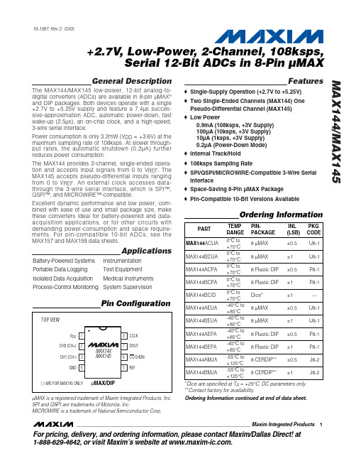
6 5
GND 4
( ) ARE FOR MAX145 ONLY
µMAX/DIP
*Dice are specified at TA = +25°C, DC parameters only. **Contact factory for availability. Ordering Information continued at end of data sheet.
ELECTRICAL CHARACTERISTICS
(V DD = +2.7V to +5.25V, V REF = 2.5V, 0.1µF capacitor at REF, f SCLK = 2.17MHz, 16 clocks/conversion cycle (108ksps), CH- = GND for MAX145, TA = TMIN to TMAX, unless otherwise noted. Typical values are at TA = +25°C.) PARAMETER DC ACCURACY (Note 1) Resolution Relative Accuracy (Note 2) Differential Nonlinearity Offset Error Gain Error Gain Temperature Coefficient Channel-to-Channel Offset Matching Channel-to-Channel Gain Matching (Note 3) ±0.8 ±0.05 ±0.05 RES INL DNL MAX14_A MAX14_B No missing codes over temperature 12 ±0.5 ±1 ±0.75 ±3 ±3 Bits LSB LSB LSB LSB ppm/°C LSB LSB SYMBOL CONDITIONS MIN TYP MAX UNITS
MAX485CPA+中文资料
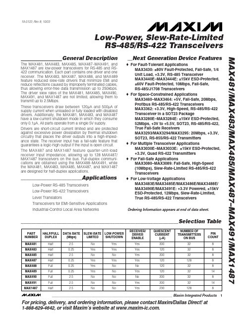
For pricing, delivery, and ordering information,please contact Maxim/Dallas Direct!at 1-888-629-4642, or visit Maxim’s website at .General DescriptionThe MAX481, MAX483, MAX485, MAX487–MAX491, and MAX1487 are low-power transceivers for RS-485 and RS-422 communication. Each part contains one driver and one receiver. The MAX483, MAX487, MAX488, and MAX489feature reduced slew-rate drivers that minimize EMI and reduce reflections caused by improperly terminated cables,thus allowing error-free data transmission up to 250kbps.The driver slew rates of the MAX481, MAX485, MAX490,MAX491, and MAX1487 are not limited, allowing them to transmit up to 2.5Mbps.These transceivers draw between 120µA and 500µA of supply current when unloaded or fully loaded with disabled drivers. Additionally, the MAX481, MAX483, and MAX487have a low-current shutdown mode in which they consume only 0.1µA. All parts operate from a single 5V supply.Drivers are short-circuit current limited and are protected against excessive power dissipation by thermal shutdown circuitry that places the driver outputs into a high-imped-ance state. The receiver input has a fail-safe feature that guarantees a logic-high output if the input is open circuit.The MAX487 and MAX1487 feature quarter-unit-load receiver input impedance, allowing up to 128 MAX487/MAX1487 transceivers on the bus. Full-duplex communi-cations are obtained using the MAX488–MAX491, while the MAX481, MAX483, MAX485, MAX487, and MAX1487are designed for half-duplex applications.________________________ApplicationsLow-Power RS-485 Transceivers Low-Power RS-422 Transceivers Level TranslatorsTransceivers for EMI-Sensitive Applications Industrial-Control Local Area Networks__Next Generation Device Features♦For Fault-Tolerant ApplicationsMAX3430: ±80V Fault-Protected, Fail-Safe, 1/4Unit Load, +3.3V, RS-485 TransceiverMAX3440E–MAX3444E: ±15kV ESD-Protected,±60V Fault-Protected, 10Mbps, Fail-Safe, RS-485/J1708 Transceivers♦For Space-Constrained ApplicationsMAX3460–MAX3464: +5V, Fail-Safe, 20Mbps,Profibus RS-485/RS-422 TransceiversMAX3362: +3.3V, High-Speed, RS-485/RS-422Transceiver in a SOT23 PackageMAX3280E–MAX3284E: ±15kV ESD-Protected,52Mbps, +3V to +5.5V, SOT23, RS-485/RS-422,True Fail-Safe ReceiversMAX3293/MAX3294/MAX3295: 20Mbps, +3.3V,SOT23, RS-855/RS-422 Transmitters ♦For Multiple Transceiver ApplicationsMAX3030E–MAX3033E: ±15kV ESD-Protected,+3.3V, Quad RS-422 Transmitters ♦For Fail-Safe ApplicationsMAX3080–MAX3089: Fail-Safe, High-Speed (10Mbps), Slew-Rate-Limited RS-485/RS-422Transceivers♦For Low-Voltage ApplicationsMAX3483E/MAX3485E/MAX3486E/MAX3488E/MAX3490E/MAX3491E: +3.3V Powered, ±15kV ESD-Protected, 12Mbps, Slew-Rate-Limited,True RS-485/RS-422 TransceiversMAX481/MAX483/MAX485/MAX487–MAX491/MAX1487Low-Power, Slew-Rate-Limited RS-485/RS-422 Transceivers______________________________________________________________Selection Table19-0122; Rev 8; 10/03Ordering Information appears at end of data sheet.M A X 481/M A X 483/M A X 485/M A X 487–M A X 491/M A X 1487Low-Power, Slew-Rate-Limited RS-485/RS-422 Transceivers 2_______________________________________________________________________________________ABSOLUTE MAXIMUM RATINGSSupply Voltage (V CC ).............................................................12V Control Input Voltage (RE , DE)...................-0.5V to (V CC + 0.5V)Driver Input Voltage (DI).............................-0.5V to (V CC + 0.5V)Driver Output Voltage (A, B)...................................-8V to +12.5V Receiver Input Voltage (A, B).................................-8V to +12.5V Receiver Output Voltage (RO).....................-0.5V to (V CC +0.5V)Continuous Power Dissipation (T A = +70°C)8-Pin Plastic DIP (derate 9.09mW/°C above +70°C)....727mW 14-Pin Plastic DIP (derate 10.00mW/°C above +70°C)..800mW 8-Pin SO (derate 5.88mW/°C above +70°C).................471mW14-Pin SO (derate 8.33mW/°C above +70°C)...............667mW 8-Pin µMAX (derate 4.1mW/°C above +70°C)..............830mW 8-Pin CERDIP (derate 8.00mW/°C above +70°C).........640mW 14-Pin CERDIP (derate 9.09mW/°C above +70°C).......727mW Operating Temperature RangesMAX4_ _C_ _/MAX1487C_ A...............................0°C to +70°C MAX4__E_ _/MAX1487E_ A.............................-40°C to +85°C MAX4__MJ_/MAX1487MJA...........................-55°C to +125°C Storage Temperature Range.............................-65°C to +160°C Lead Temperature (soldering, 10sec).............................+300°CDC ELECTRICAL CHARACTERISTICS(V CC = 5V ±5%, T A = T MIN to T MAX , unless otherwise noted.) (Notes 1, 2)Stresses beyond those listed under “Absolute Maximum Ratings” may cause permanent damage to the device. These are stress ratings only, and functional operation of the device at these or any other conditions beyond those indicated in the operational sections of the specifications is not implied. Exposure to absolute maximum rating conditions for extended periods may affect device reliability.V V IN = -7VV IN = 12V V IN = -7V V IN = 12V Input Current (A, B)I IN2V TH k Ω48-7V ≤V CM ≤12V, MAX487/MAX1487R INReceiver Input Resistance -7V ≤V CM ≤12V, all devices except MAX487/MAX1487R = 27Ω(RS-485), Figure 40.4V ≤V O ≤2.4VR = 50Ω(RS-422)I O = 4mA, V ID = -200mV I O = -4mA, V ID = 200mV V CM = 0V-7V ≤V CM ≤12V DE, DI, RE DE, DI, RE MAX487/MAX1487,DE = 0V, V CC = 0V or 5.25VDE, DI, RE R = 27Ωor 50Ω, Figure 4R = 27Ωor 50Ω, Figure 4R = 27Ωor 50Ω, Figure 4DE = 0V;V CC = 0V or 5.25V,all devices except MAX487/MAX1487CONDITIONSk Ω12µA ±1I OZRThree-State (high impedance)Output Current at ReceiverV 0.4V OL Receiver Output Low Voltage 3.5V OH Receiver Output High Voltage mV 70∆V TH Receiver Input Hysteresis V -0.20.2Receiver Differential Threshold Voltage-0.2mA 0.25mA-0.81.01.55V OD2Differential Driver Output (with load)V 2V 5V OD1Differential Driver Output (no load)µA±2I IN1Input CurrentV 0.8V IL Input Low Voltage V 2.0V IH Input High Voltage V 0.2∆V OD Change in Magnitude of Driver Common-Mode Output Voltage for Complementary Output States V 0.2∆V OD Change in Magnitude of Driver Differential Output Voltage for Complementary Output States V 3V OC Driver Common-Mode Output VoltageUNITS MINTYPMAX SYMBOL PARAMETERMAX481/MAX483/MAX485/MAX487–MAX491/MAX1487Low-Power, Slew-Rate-Limited RS-485/RS-422 Transceivers_______________________________________________________________________________________3SWITCHING CHARACTERISTICS—MAX481/MAX485, MAX490/MAX491, MAX1487(V CC = 5V ±5%, T A = T MIN to T MAX , unless otherwise noted.) (Notes 1, 2)DC ELECTRICAL CHARACTERISTICS (continued)(V CC = 5V ±5%, T A = T MIN to T MAX , unless otherwise noted.) (Notes 1, 2)ns 103060t PHLDriver Rise or Fall Time Figures 6 and 8, R DIFF = 54Ω, C L1= C L2= 100pF ns MAX490M, MAX491M MAX490C/E, MAX491C/E2090150MAX481, MAX485, MAX1487MAX490M, MAX491MMAX490C/E, MAX491C/E MAX481, MAX485, MAX1487Figures 6 and 8, R DIFF = 54Ω,C L1= C L2= 100pF MAX481 (Note 5)Figures 5 and 11, C RL = 15pF, S2 closedFigures 5 and 11, C RL = 15pF, S1 closed Figures 5 and 11, C RL = 15pF, S2 closed Figures 5 and 11, C RL = 15pF, S1 closed Figures 6 and 10, R DIFF = 54Ω,C L1= C L2= 100pFFigures 6 and 8,R DIFF = 54Ω,C L1= C L2= 100pF Figures 6 and 10,R DIFF = 54Ω,C L1= C L2= 100pF CONDITIONS ns 510t SKEW ns50200600t SHDNTime to ShutdownMbps 2.5f MAX Maximum Data Rate ns 2050t HZ Receiver Disable Time from High ns 103060t PLH 2050t LZ Receiver Disable Time from Low ns 2050t ZH Driver Input to Output Receiver Enable to Output High ns 2050t ZL Receiver Enable to Output Low 2090200ns ns 134070t HZ t SKD Driver Disable Time from High |t PLH - t PHL |DifferentialReceiver Skewns 4070t LZ Driver Disable Time from Low ns 4070t ZL Driver Enable to Output Low 31540ns51525ns 31540t R , t F 2090200Driver Output Skew to Output t PLH , t PHL Receiver Input to Output4070t ZH Driver Enable to Output High UNITS MIN TYP MAX SYMBOL PARAMETERFigures 7 and 9, C L = 100pF, S2 closed Figures 7 and 9, C L = 100pF, S1 closed Figures 7 and 9, C L = 15pF, S1 closed Figures 7 and 9, C L = 15pF, S2 closedM A X 481/M A X 483/M A X 485/M A X 487–M A X 491/M A X 1487Low-Power, Slew-Rate-Limited RS-485/RS-422 Transceivers 4_______________________________________________________________________________________SWITCHING CHARACTERISTICS—MAX483, MAX487/MAX488/MAX489(V CC = 5V ±5%, T A = T MIN to T MAX , unless otherwise noted.) (Notes 1, 2)SWITCHING CHARACTERISTICS—MAX481/MAX485, MAX490/MAX491, MAX1487 (continued)(V CC = 5V ±5%, T A = T MIN to T MAX , unless otherwise noted.) (Notes 1, 2)3001000Figures 7 and 9, C L = 100pF, S2 closed Figures 7 and 9, C L = 100pF, S1 closed Figures 5 and 11, C L = 15pF, S2 closed,A - B = 2VCONDITIONSns 40100t ZH(SHDN)Driver Enable from Shutdown toOutput High (MAX481)nsFigures 5 and 11, C L = 15pF, S1 closed,B - A = 2Vt ZL(SHDN)Receiver Enable from Shutdownto Output Low (MAX481)ns 40100t ZL(SHDN)Driver Enable from Shutdown toOutput Low (MAX481)ns 3001000t ZH(SHDN)Receiver Enable from Shutdownto Output High (MAX481)UNITS MINTYP MAX SYMBOLPARAMETERt PLH t SKEW Figures 6 and 8, R DIFF = 54Ω,C L1= C L2= 100pFt PHL Figures 6 and 8, R DIFF = 54Ω,C L1= C L2= 100pFDriver Input to Output Driver Output Skew to Output ns 100800ns ns 2000MAX483/MAX487, Figures 7 and 9,C L = 100pF, S2 closedt ZH(SHDN)Driver Enable from Shutdown to Output High2502000ns2500MAX483/MAX487, Figures 5 and 11,C L = 15pF, S1 closedt ZL(SHDN)Receiver Enable from Shutdown to Output Lowns 2500MAX483/MAX487, Figures 5 and 11,C L = 15pF, S2 closedt ZH(SHDN)Receiver Enable from Shutdown to Output Highns 2000MAX483/MAX487, Figures 7 and 9,C L = 100pF, S1 closedt ZL(SHDN)Driver Enable from Shutdown to Output Lowns 50200600MAX483/MAX487 (Note 5) t SHDN Time to Shutdownt PHL t PLH , t PHL < 50% of data period Figures 5 and 11, C RL = 15pF, S2 closed Figures 5 and 11, C RL = 15pF, S1 closed Figures 5 and 11, C RL = 15pF, S2 closed Figures 5 and 11, C RL = 15pF, S1 closed Figures 7 and 9, C L = 15pF, S2 closed Figures 6 and 10, R DIFF = 54Ω,C L1= C L2= 100pFFigures 7 and 9, C L = 15pF, S1 closed Figures 7 and 9, C L = 100pF, S1 closed Figures 7 and 9, C L = 100pF, S2 closed CONDITIONSkbps 250f MAX 2508002000Maximum Data Rate ns 2050t HZ Receiver Disable Time from High ns 25080020002050t LZ Receiver Disable Time from Low ns 2050t ZH Receiver Enable to Output High ns 2050t ZL Receiver Enable to Output Low ns ns 1003003000t HZ t SKD Driver Disable Time from High I t PLH - t PHL I DifferentialReceiver SkewFigures 6 and 10, R DIFF = 54Ω,C L1= C L2= 100pFns 3003000t LZ Driver Disable Time from Low ns 2502000t ZL Driver Enable to Output Low ns Figures 6 and 8, R DIFF = 54Ω,C L1= C L2= 100pFns 2502000t R , t F 2502000Driver Rise or Fall Time ns t PLH Receiver Input to Output2502000t ZH Driver Enable to Output High UNITS MIN TYP MAX SYMBOL PARAMETERMAX481/MAX483/MAX485/MAX487–MAX491/MAX1487Low-Power, Slew-Rate-Limited RS-485/RS-422 Transceivers_______________________________________________________________________________________530002.5OUTPUT CURRENT vs.RECEIVER OUTPUT LOW VOLTAGE525M A X 481-01OUTPUT LOW VOLTAGE (V)O U T P U T C U R R E N T (m A )1.515100.51.02.0203540450.90.1-50-252575RECEIVER OUTPUT LOW VOLTAGE vs.TEMPERATURE0.30.7TEMPERATURE (°C)O U T P U TL O W V O L T A G E (V )500.50.80.20.60.40100125-20-41.5 2.0 3.0 5.0OUTPUT CURRENT vs.RECEIVER OUTPUT HIGH VOLTAGE-8-16M A X 481-02OUTPUT HIGH VOLTAGE (V)O U T P U T C U R R E N T (m A )2.5 4.0-12-18-6-14-10-203.54.5 4.83.2-50-252575RECEIVER OUTPUT HIGH VOLTAGE vs.TEMPERATURE3.64.4TEMPERATURE (°C)O U T P UT H I G H V O L T A G E (V )0504.04.63.44.23.83.01001259000 1.0 3.0 4.5DRIVER OUTPUT CURRENT vs.DIFFERENTIAL OUTPUT VOLTAGE1070M A X 481-05DIFFERENTIAL OUTPUT VOLTAGE (V)O U T P U T C U R R E N T (m A )2.0 4.05030806040200.5 1.5 2.53.5 2.31.5-50-2525125DRIVER DIFFERENTIAL OUTPUT VOLTAGEvs. TEMPERATURE1.72.1TEMPERATURE (°C)D I F FE R E N T I A L O U T P U T V O L T A G E (V )751.92.21.62.01.8100502.4__________________________________________Typical Operating Characteristics(V CC = 5V, T A = +25°C, unless otherwise noted.)NOTES FOR ELECTRICAL/SWITCHING CHARACTERISTICSNote 1:All currents into device pins are positive; all currents out of device pins are negative. All voltages are referenced to deviceground unless otherwise specified.Note 2:All typical specifications are given for V CC = 5V and T A = +25°C.Note 3:Supply current specification is valid for loaded transmitters when DE = 0V.Note 4:Applies to peak current. See Typical Operating Characteristics.Note 5:The MAX481/MAX483/MAX487 are put into shutdown by bringing RE high and DE low. If the inputs are in this state for lessthan 50ns, the parts are guaranteed not to enter shutdown. If the inputs are in this state for at least 600ns, the parts are guaranteed to have entered shutdown. See Low-Power Shutdown Mode section.M A X 481/M A X 483/M A X 485/M A X 487–M A X 491/M A X 1487Low-Power, Slew-Rate-Limited RS-485/RS-422 Transceivers 6___________________________________________________________________________________________________________________Typical Operating Characteristics (continued)(V CC = 5V, T A = +25°C, unless otherwise noted.)120008OUTPUT CURRENT vs.DRIVER OUTPUT LOW VOLTAGE20100M A X 481-07OUTPUT LOW VOLTAGE (V)O U T P U T C U R R E N T (m A )6604024801012140-1200-7-5-15OUTPUT CURRENT vs.DRIVER OUTPUT HIGH VOLTAGE-20-80M A X 481-08OUTPUT HIGH VOLTAGE (V)O U T P U T C U R R E N T (m A )-31-603-6-4-2024-100-40100-40-60-2040100120MAX1487SUPPLY CURRENT vs. TEMPERATURE300TEMPERATURE (°C)S U P P L Y C U R R E N T (µA )20608050020060040000140100-50-2550100MAX481/MAX485/MAX490/MAX491SUPPLY CURRENT vs. TEMPERATURE300TEMPERATURE (°C)S U P P L Y C U R R E N T (µA )257550020060040000125100-50-2550100MAX483/MAX487–MAX489SUPPLY CURRENT vs. TEMPERATURE300TEMPERATURE (°C)S U P P L Y C U R R E N T (µA )257550020060040000125MAX481/MAX483/MAX485/MAX487–MAX491/MAX1487Low-Power, Slew-Rate-Limited RS-485/RS-422 Transceivers_______________________________________________________________________________________7______________________________________________________________Pin DescriptionFigure 1. MAX481/MAX483/MAX485/MAX487/MAX1487 Pin Configuration and Typical Operating CircuitM A X 481/M A X 483/M A X 485/M A X 487–M A X 491/M A X 1487__________Applications InformationThe MAX481/MAX483/MAX485/MAX487–MAX491 and MAX1487 are low-power transceivers for RS-485 and RS-422 communications. The MAX481, MAX485, MAX490,MAX491, and MAX1487 can transmit and receive at data rates up to 2.5Mbps, while the MAX483, MAX487,MAX488, and MAX489 are specified for data rates up to 250kbps. The MAX488–MAX491 are full-duplex trans-ceivers while the MAX481, MAX483, MAX485, MAX487,and MAX1487 are half-duplex. In addition, Driver Enable (DE) and Receiver Enable (RE) pins are included on the MAX481, MAX483, MAX485, MAX487, MAX489,MAX491, and MAX1487. When disabled, the driver and receiver outputs are high impedance.MAX487/MAX1487:128 Transceivers on the BusThe 48k Ω, 1/4-unit-load receiver input impedance of the MAX487 and MAX1487 allows up to 128 transceivers on a bus, compared to the 1-unit load (12k Ωinput impedance) of standard RS-485 drivers (32 trans-ceivers maximum). Any combination of MAX487/MAX1487 and other RS-485 transceivers with a total of 32 unit loads or less can be put on the bus. The MAX481/MAX483/MAX485 and MAX488–MAX491 have standard 12k ΩReceiver Input impedance.Low-Power, Slew-Rate-Limited RS-485/RS-422 Transceivers 8_______________________________________________________________________________________Figure 2. MAX488/MAX490 Pin Configuration and Typical Operating CircuitFigure 3. MAX489/MAX491 Pin Configuration and Typical Operating CircuitMAX483/MAX487/MAX488/MAX489:Reduced EMI and ReflectionsThe MAX483 and MAX487–MAX489 are slew-rate limit-ed, minimizing EMI and reducing reflections caused by improperly terminated cables. Figure 12 shows the dri-ver output waveform and its Fourier analysis of a 150kHz signal transmitted by a MAX481, MAX485,MAX490, MAX491, or MAX1487. High-frequency har-monics with large amplitudes are evident. Figure 13shows the same information displayed for a MAX483,MAX487, MAX488, or MAX489 transmitting under the same conditions. Figure 13’s high-frequency harmonics have much lower amplitudes, and the potential for EMI is significantly reduced.MAX481/MAX483/MAX485/MAX487–MAX491/MAX1487Low-Power, Slew-Rate-Limited RS-485/RS-422 Transceivers_______________________________________________________________________________________9_________________________________________________________________Test CircuitsFigure 4. Driver DC Test Load Figure 5. Receiver Timing Test LoadFigure 6. Driver/Receiver Timing Test Circuit Figure 7. Driver Timing Test LoadM A X 481/M A X 483/M A X 485/M A X 487–M A X 491/M A X 1487Low-Power, Slew-Rate-Limited RS-485/RS-422 Transceivers 10_______________________________________________________Switching Waveforms_________________Function Tables (MAX481/MAX483/MAX485/MAX487/MAX1487)Figure 8. Driver Propagation DelaysFigure 9. Driver Enable and Disable Times (except MAX488 and MAX490)Figure 10. Receiver Propagation DelaysFigure 11. Receiver Enable and Disable Times (except MAX488and MAX490)Table 1. TransmittingTable 2. ReceivingLow-Power Shutdown Mode (MAX481/MAX483/MAX487)A low-power shutdown mode is initiated by bringing both RE high and DE low. The devices will not shut down unless both the driver and receiver are disabled.In shutdown, the devices typically draw only 0.1µA of supply current.RE and DE may be driven simultaneously; the parts are guaranteed not to enter shutdown if RE is high and DE is low for less than 50ns. If the inputs are in this state for at least 600ns, the parts are guaranteed to enter shutdown.For the MAX481, MAX483, and MAX487, the t ZH and t ZL enable times assume the part was not in the low-power shutdown state (the MAX485/MAX488–MAX491and MAX1487 can not be shut down). The t ZH(SHDN)and t ZL(SHDN)enable times assume the parts were shut down (see Electrical Characteristics ).It takes the drivers and receivers longer to become enabled from the low-power shutdown state (t ZH(SHDN ), t ZL(SHDN)) than from the operating mode (t ZH , t ZL ). (The parts are in operating mode if the –R —E –,DE inputs equal a logical 0,1 or 1,1 or 0, 0.)Driver Output ProtectionExcessive output current and power dissipation caused by faults or by bus contention are prevented by two mechanisms. A foldback current limit on the output stage provides immediate protection against short cir-cuits over the whole common-mode voltage range (see Typical Operating Characteristics ). In addition, a ther-mal shutdown circuit forces the driver outputs into a high-impedance state if the die temperature rises excessively.Propagation DelayMany digital encoding schemes depend on the differ-ence between the driver and receiver propagation delay times. Typical propagation delays are shown in Figures 15–18 using Figure 14’s test circuit.The difference in receiver delay times, | t PLH - t PHL |, is typically under 13ns for the MAX481, MAX485,MAX490, MAX491, and MAX1487 and is typically less than 100ns for the MAX483 and MAX487–MAX489.The driver skew times are typically 5ns (10ns max) for the MAX481, MAX485, MAX490, MAX491, and MAX1487, and are typically 100ns (800ns max) for the MAX483 and MAX487–MAX489.MAX481/MAX483/MAX485/MAX487–MAX491/MAX1487Low-Power, Slew-Rate-Limited RS-485/RS-422 Transceivers______________________________________________________________________________________1110dB/div0Hz5MHz500kHz/div10dB/div0Hz5MHz500kHz/divFigure 12. Driver Output Waveform and FFT Plot of MAX481/MAX485/MAX490/MAX491/MAX1487 Transmitting a 150kHz SignalFigure 13. Driver Output Waveform and FFT Plot of MAX483/MAX487–MAX489 Transmitting a 150kHz SignalM A X 481/M A X 483/M A X 485/M A X 487–M A X 491/M A X 1487Low-Power, Slew-Rate-Limited RS-485/RS-422 Transceivers 12______________________________________________________________________________________V CC = 5V T A = +25°CV CC = 5V T A = +25°CV CC = 5V T A = +25°CV CC = 5V T A = +25°CFigure 14. Receiver Propagation Delay Test CircuitFigure 15. MAX481/MAX485/MAX490/MAX491/MAX1487Receiver t PHLFigure 16. MAX481/MAX485/MAX490/MAX491/MAX1487Receiver t PLHPHL Figure 18. MAX483, MAX487–MAX489 Receiver t PLHLine Length vs. Data RateThe RS-485/RS-422 standard covers line lengths up to 4000 feet. For line lengths greater than 4000 feet, see Figure 23.Figures 19 and 20 show the system differential voltage for the parts driving 4000 feet of 26AWG twisted-pair wire at 110kHz into 120Ωloads.Typical ApplicationsThe MAX481, MAX483, MAX485, MAX487–MAX491, and MAX1487 transceivers are designed for bidirectional data communications on multipoint bus transmission lines.Figures 21 and 22 show typical network applications circuits. These parts can also be used as line repeaters, with cable lengths longer than 4000 feet, as shown in Figure 23.To minimize reflections, the line should be terminated at both ends in its characteristic impedance, and stub lengths off the main line should be kept as short as possi-ble. The slew-rate-limited MAX483 and MAX487–MAX489are more tolerant of imperfect termination.MAX481/MAX483/MAX485/MAX487–MAX491/MAX1487Low-Power, Slew-Rate-Limited RS-485/RS-422 Transceivers______________________________________________________________________________________13DIV Y -V ZRO5V 0V1V0V -1V5V 0V2µs/divFigure 19. MAX481/MAX485/MAX490/MAX491/MAX1487 System Differential Voltage at 110kHz Driving 4000ft of Cable Figure 20. MAX483, MAX487–MAX489 System Differential Voltage at 110kHz Driving 4000ft of CableFigure 21. MAX481/MAX483/MAX485/MAX487/MAX1487 Typical Half-Duplex RS-485 NetworkM A X 481/M A X 483/M A X 485/M A X 487–M A X 491/M A X 1487Low-Power, Slew-Rate-Limited RS-485/RS-422 Transceivers 14______________________________________________________________________________________Figure 22. MAX488–MAX491 Full-Duplex RS-485 NetworkFigure 23. Line Repeater for MAX488–MAX491Isolated RS-485For isolated RS-485 applications, see the MAX253 and MAX1480 data sheets.MAX481/MAX483/MAX485/MAX487–MAX491/MAX1487Low-Power, Slew-Rate-Limited RS-485/RS-422 Transceivers______________________________________________________________________________________15_______________Ordering Information_________________Chip TopographiesMAX481/MAX483/MAX485/MAX487/MAX1487N.C. RO 0.054"(1.372mm)0.080"(2.032mm)DE DIGND B N.C.V CCARE * Contact factory for dice specifications.__Ordering Information (continued)M A X 481/M A X 483/M A X 485/M A X 487–M A X 491/M A X 1487Low-Power, Slew-Rate-Limited RS-485/RS-422 Transceivers 16______________________________________________________________________________________TRANSISTOR COUNT: 248SUBSTRATE CONNECTED TO GNDMAX488/MAX490B RO 0.054"(1.372mm)0.080"(2.032mm)N.C. DIGND Z A V CCYN.C._____________________________________________Chip Topographies (continued)MAX489/MAX491B RO 0.054"(1.372mm)0.080"(2.032mm)DE DIGND Z A V CCYREMAX481/MAX483/MAX485/MAX487–MAX491/MAX1487Low-Power, Slew-Rate-Limited RS-485/RS-422 Transceivers______________________________________________________________________________________17Package Information(The package drawing(s) in this data sheet may not reflect the most current specifications. For the latest package outline information go to /packages .)S O I C N .E P SM A X 481/M A X 483/M A X 485/M A X 487–M A X 491/M A X 1487Low-Power, Slew-Rate-Limited RS-485/RS-422 Transceivers 18______________________________________________________________________________________Package Information (continued)(The package drawing(s) in this data sheet may not reflect the most current specifications. For the latest package outline information go to /packages .)MAX481/MAX483/MAX485/MAX487–MAX491Low-Power, Slew-Rate-Limited RS-485/RS-422 TransceiversMaxim cannot assume responsibility for use of any circuitry other than circuitry entirely embodied in a Maxim product. No circuit patent licenses are implied. Maxim reserves the right to change the circuitry and specifications without notice at any time.Maxim Integrated Products, 120 San Gabriel Drive, Sunnyvale, CA 94086 408-737-7600 ____________________19©2003 Maxim Integrated ProductsPrinted USAis a registered trademark of Maxim Integrated Products.M A X 481/M A X 483/M A X 485/M A X 487–M A X 491/M A X 1487P D I P N .E PSPackage Information (continued)(The package drawing(s) in this data sheet may not reflect the most current specifications. For the latest package outline information go to /packages .)。
MAX1400EAI+;MAX1400CAI+T;MAX1400EAI+T;MAX1400CAI+;中文规格书,Datasheet资料

MAX1400+5V , 18-Bit, Low-Power, Multichannel,Oversampling (Sigma-Delta) ADC________________________________________________________________Maxim Integrated Products119-1430; Rev 1; 7/02General DescriptionThe MAX1400 18-bit, low-power, multichannel, serial-output ADC uses a sigma-delta modulator with a digital decimation filter to achieve true 16-bit accuracy. The user-selectable decimation factor of the digital filter allows the conversion resolution to be reduced in exchange for a higher output data rate. The device achieves true 16-bit performance at an output data rate of up to 480sps. In addition, the modulator sampling frequency may be optimized for either lowest power dissipation or highest throughput rate. The MAX1400operates from +5V.This device offers three fully differential input channels that can be independently programmed with a gain between +1V/V and +128V/V. Furthermore, it can com-pensate an input-referred DC offset (such as system off-set) up to 117% of the selected full-scale range. These three differential channels may also be configured to operate as five pseudo-differential input channels. Two additional, fully differential system-calibration channels are provided for gain and offset error correction. External access is provided to the multiplexer (mux) output to facilitate additional signal processing.The MAX1400 can be configured to scan all signal inputs sequentially and provide the results through the serial interface with minimum communications overhead. When used with a 2.4576MH z or 1.024MH z master clock, the digital decimation filter can be programmed to produce zeros in its frequency response at the line fre-quency and associated harmonics, ensuring excellent line rejection without the need for further post-filtering.The MAX1400 comes in a 28-pin SSOP package.ApplicationsPortable Industrial Instruments Portable Weigh Scales Loop-Powered Systems Pressure TransducersFeatureso 18-Bit Resolution, Sigma-Delta ADC o 16-Bit Performance with No Missing Codes to 480sps o Low Quiescent Current250µA (operating mode)2µA (power-down mode)o 3 Fully Differential or 5 Pseudo-Differential Signal Input Channels o 2 Additional Fully Differential Calibration Channels/Auxiliary Input Channels o Access to the Mux Output/ADC Input o Programmable Gain and Offset o Fully Differential Reference Inputs o Converts Continuously or On Command o Automatic Channel Scanning and Continuous Data Output Mode o Operates with +5V Analog Supply and +3V or +5V Digital Supplyo SPI™/QSPI™-Compatible 3-Wire Serial Interface o 28-Pin SSOP PackageSPI and QSPI are trademarks of Motorola, Inc.Pin ConfigurationOrdering InformationFor pricing, delivery, and ordering information,please contact Maxim/Dallas Direct!at 1-888-629-4642, or visit Maxim’s website at .M A X 1400+5V , 18-Bit, Low-Power, Multichannel, Oversampling (Sigma-Delta) ADC 2_______________________________________________________________________________________ABSOLUTE MAXIMUM RATINGSELECTRICAL CHARACTERISTICS(V+ = +5V ±5%, V DD = +2.7V to +5.25V, V REFIN+= +2.50V, REFIN- = AGND, f CLKIN = 2.4576MHz, T A = T MIN to T MAX , unless other-wise noted. Typical values are at T A = +25°C.)Stresses beyond those listed under “Absolute Maximum Ratings” may cause permanent damage to the device. These are stress ratings only, and functional operation of the device at these or any other conditions beyond those indicated in the operational sections of the specifications is not implied. Exposure to absolute maximum rating conditions for extended periods may affect device reliability.V+ to AGND, DGND.................................................-0.3V to +6V V DD to AGND, DGND...............................................-0.3V to +6V AGND to DGND.....................................................-0.3V to +0.3V Analog Inputs to AGND................................-0.3V to (V+ + 0.3V)Analog Outputs to AGND.............................-0.3V to (V+ + 0.3V)Reference Inputs to AGND...........................-0.3V to (V+ + 0.3V)CLKIN and CLKOUT to DGND...................-0.3V to (V DD + 0.3V)All Other Digital Inputs to DGND..............................-0.3V to +6V All Digital Outputs to DGND.......................-0.3V to (V DD + 0.3V)Maximum Current Input into Any Pin..................................50mA Continuous Power Dissipation (T A = +70°C)28-Pin SSOP (derate 9.52mW/°C above +70°C)........524mW Operating Temperature RangesMAX1400CAI .....................................................0°C to +70°C MAX1400EAI...................................................-40°C to +85°C Storage Temperature Range.............................-60°C to +150°C Lead Temperature (soldering, 10s).................................+300°CMAX1400+5V , 18-Bit, Low-Power, Multichannel,Oversampling (Sigma-Delta) ADC________________________________________________________________________________________3ELECTRICAL CHARACTERISTICS (continued)(V+ = +5V ±5%, V DD = +2.7V to +5.25V, V REFIN+= +2.50V, REFIN- = AGND, f CLKIN = 2.4576MHz, T A = T MIN to T MAX , unless other-wise noted. Typical values are at T A = +25°C.)M A X 1400+5V , 18-Bit, Low-Power, Multichannel, Oversampling (Sigma-Delta) ADC 4_______________________________________________________________________________________ELECTRICAL CHARACTERISTICS (continued)(V+ = +5V ±5%, V DD = +2.7V to +5.25V, V REFIN+= +2.50V, REFIN- = AGND, f CLKIN = 2.4576MHz, T A = T MIN to T MAX , unless other-wise noted. Typical values are at T = +25°C.)MAX1400+5V , 18-Bit, Low-Power, Multichannel,Oversampling (Sigma-Delta) ADC_______________________________________________________________________________________5ELECTRICAL CHARACTERISTICS (continued)(V+ = +5V ±5%, V DD = +2.7V to +5.25V, V REFIN+= +2.50V, REFIN- = AGND, f CLKIN = 2.4576MHz, T A = T MIN to T MAX , unless other-wise noted. Typical values are at T A = +25°C.)M A X 1400+5V , 18-Bit, Low-Power, Multichannel, Oversampling (Sigma-Delta) ADC 6_______________________________________________________________________________________Note 1:Nominal gain is 0.98. This ensures a full-scale input voltage may be applied to the part under all conditions without caus-ing saturation of the digital output data.Note 2:Positive Full-Scale Error includes zero-scale errors (unipolar offset error or bipolar zero error) and applies to both unipolarand bipolar input ranges. This error does not include the nominal gain of 0.98.Note 3:Full-Scale Drift includes zero-scale drift (unipolar offset drift or bipolar zero drift) and applies to both unipolar and bipolarinput ranges.Note 4:Gain Error does not include zero-scale errors. It is calculated as (full-scale error - unipolar offset error) for unipolar rangesand as (full-scale error - bipolar zero error) for bipolar ranges. This error does not include the nominal gain of 0.98.Note 5:Gain-Error Drift does not include unipolar offset drift or bipolar zero drift. It is effectively the drift of the part if zero-scaleerror is removed.Note 6:Use of the offset DAC does not imply that any input may be taken below AGND.Note 7:Additional noise added by the offset DAC is dependent on the filter cutoff, gain, and DAC setting. No noise is added for aDAC code of 0000.Note 8:Guaranteed by design or characterization; not production tested.Note 9:The input voltage must be within the Absolute Input Voltage Range specification.Note 10:All AIN and REFIN pins have identical input structures. Leakage is production tested only for the AIN3, AIN4, AIN5,CALGAIN, and CALOFF inputs.Note 11:The dynamic load presented by the MAX1400 analog inputs for each gain setting is discussed in detail in the SwitchingNetwork section .Values are provided for the maximum allowable external series resistance. Note that this value does not include any additional capacitance added by the user to the MUXOUT_ or ADCIN_ pins.Note 12:The input voltage range for the analog inputs is with respect to the voltage on the negative input of its respective differen-tial or pseudo-differential pair. Table 5 shows which inputs form differential pairs.Note 13:V REF = V REFIN+- V REFIN-.Note 14:These specifications apply to CLKOUT only when driving a single CMOS load.Note 15:The burn-out currents require a 500mV overhead between the analog input voltage and both V+ and AGND to operatecorrectly.ELECTRICAL CHARACTERISTICS (continued)(V+ = +5V ±5%, V DD = +2.7V to +5.25V, V REFIN+= +2.50V, REFIN- = AGND, f CLKIN = 2.4576MHz, T A = T MIN to T MAX , unless other-MAX1400+5V , 18-Bit, Low-Power, Multichannel,Oversampling (Sigma-Delta) ADC_______________________________________________________________________________________7Note 16:Measured at DC in the selected passband. PSR at 50Hz will exceed 120dB with filter notches of 25Hz or 50Hz and FASTbit = 0. PSR at 60Hz exceeds 120dB with filter notches of 20Hz or 60Hz and FAST bit = 0.Note 17:PSR depends on gain. For a gain of +1V/V, PSR is 70dB typical. For a gain of +2V/V, PSR is 75dB typical. For a gain of+4V/V, PSR is 80dB typical. For gains of +8V/V to +128V/V, PSR is 85dB typical.Note 18:Standby power-dissipation and current specifications are valid only with CLKIN driven by an external clock and with theexternal clock stopped. If the clock continues to run in standby mode, the power dissipation will be considerably higher.When used with a resonator or crystal between CLKIN and CLKOUT, the actual power dissipation and I DD in standby mode depends on the resonator or crystal type.TIMING CHARACTERISTICS(V+ = +5V ±5%, V DD = +2.7V to +5.25V, AGND = DGND, f CLKIN = 2.4576MHz; input logic 0 = 0V; logic 1 = V DD , T A = T MIN to T MAX ,unless otherwise noted.) (Notes 19, 20, 21)M A X 1400+5V , 18-Bit, Low-Power, Multichannel, Oversampling (Sigma-Delta) ADC 8_______________________________________________________________________________________TIMING CHARACTERISTICS (continued)(V+ = +5V ±5%, V DD = +2.7V to +5.25V, AGND = DGND, f CLKIN = 2.4576MHz; input logic 0 = 0V; logic 1 = V DD , T A = T MIN to T MAX ,unless otherwise noted.) (Notes 19, 20, 21)Note 19:All input signals are specified with t r = t f = 5ns (10% to 90% of V DD ).Note 20:See Figure 4.Note 21:Timings shown in tables are for the case where SCLK idles high between accesses. The part may also be used with theSCLK idling low between accesses, provided CS is toggled. In this case SCLK in the timing diagrams should be inverted and the terms “SCLK Falling Edge” and “SCLK Rising Edge” exchanged in the specification tables. If CS is permanently tied low, the part should only be operated with SCLK idling high between accesses.Note 22:CLKIN duty cycle range is 45% to 55%. CLKIN must be supplied whenever the MAX1400 is not in standby mode. If noclock is present, the device can draw higher current than specified.Note 23:The MAX1400 is production tested with f CLKIN at 2.5MHz (1MHz for some I DD tests).Note 24:Measured with the load circuit of Figure 1 and defined as the time required for the output to cross the V OL or V OH limits.Note 25:For read operations, SCLK active edge is falling edge of SCLK.Note 26:Derived from the time taken by the data output to change 0.5V when loaded with the circuit of Figure 1. The number is thenextrapolated back to remove effects of charging or discharging the 50pF capacitor. This ensures that the times quoted in the timing characteristics are true bus-relinquish times and are independent of external bus loading capacitances.Note 27:INT returns high after the first read after an output update. The same data can be read again while INT is high, but becareful not to allow subsequent reads to occur close to the next output update.Figure 1. Load Circuit for Bus Relinquish Time and V OL and V OH LevelsMAX1400+5V , 18-Bit, Low-Power, Multichannel,Oversampling (Sigma-Delta) ADC_______________________________________________________________________________________9Pin Description15AIN5Analog Input Channel 5. Used as a differential or pseudo-differential input with AIN6 (see the Communications Register section).NAME FUNCTION1CLKINClock Input. A crystal can be connected across CLKIN and CLKOUT. Alternatively, drive CLKIN with a CMOS-compatible clock at a nominal frequency of 2.4576MHz or 1.024MHz, and leave CLKOUT uncon-nected. Frequencies of 4.9152MHz and 2.048MHz can be used if the X2CLK control bit is set to 1.PIN 2CLKOUTClock Output. When deriving the master clock from a crystal, connect the crystal between CLKIN andCLKOUT. In this mode, the on-chip clock signal is not available at CLKOUT. Leave CLKOUT unconnected when CLKIN is driven with an external clock.3CSChip-Select Input. Active-low logic input used to enable the digital interface. With CS hard-wired low, the MAX1400 operates in its 3-wire interface mode with SCLK, DIN and DOUT used to interface to the device.CS is used either to select the device in systems with more than one device on the serial bus, or as a frame-synchronization signal for the MAX1400 when a continuous SCLK is used.4RESETActive Low Reset Input. Drive low to reset the control logic, interface logic, digital filter and analog modu-lator to power-on status. RESET must be high and CLKIN must be toggling in order to exit reset. 5MUXOUT+Positive Analog Mux Output. The positive differential output signal from the part’s internal input multiplex-er. Use this signal in conjunction with MUXOUT- and a high-quality external amplifier for additional signal processing before conversion. Return the processed output through ADCIN+ and ADCIN-. Connect MUXOUT+ directly to ADCIN+ if external processing is not required.6MUXOUT-Negative Analog Mux Output. The negative differential output signal from the part’s internal input multi-plexer. Use this signal in conjunction with MUXOUT+ and a high-quality external amplifier for additional signal processing before conversion. Return the processed output through ADCIN+ and ADCIN-.Connect MUXOUT- directly to ADCIN- if external processing is not required.7ADCIN+Positive Analog Input. A direct input to the positive buffer and the positive differential input terminal of the ADC, bypassing the input mux. This signal forms a differential input pair with ADCIN-. Connect ADCIN+ to MUXOUT+ when direct access is not required.8ADCIN-Negative Analog Input. A direct input to the negative buffer and the negative differential input terminal of the ADC - bypassing the input mux. This signal forms a differential input pair with ADCIN+. Connect ADCIN- to MUXOUT- when direct access is not required.9AGND Analog Ground. Reference point for the analog circuitry. AGND connects to the IC substrate.10V+Analog Positive Supply Voltage (+4.75V to +5.25V)11AIN1Analog Input Channel 1. Can be used as a pseudo-differential input with AIN6 as common, or as the posi-tive input of the AIN1/AIN2 differential analog input pair (see the Communications Register section).12AIN2Analog Input Channel 2. Can be used as a pseudo-differential input with AIN6 as common, or as the neg-ative input of the AIN1/AIN2 differential analog input pair (see the Communications Register section).13AIN3Analog Input Channel 3. Can be used as a pseudo-differential input with AIN6 as common, or as the posi-tive input of the AIN3/AIN4 differential analog input pair (see the Communications Register section).14AIN4Analog Input Channel 4. Can be used as a pseudo-differential input with AIN6 as common, or as the neg-ative input of the AIN3/AIN4 differential analog input pair (see the Communications Register section).16AIN6Analog Input 6. Can be used as a common point for AIN1 through AIN5 in pseudo-differential mode, or as the negative input of the AIN5/AIN6 differential analog input pair (see the Communications Register section).M A X 1400+5V , 18-Bit, Low-Power, Multichannel, Oversampling (Sigma-Delta) ADC 10______________________________________________________________________________________Pin Description (continued)分销商库存信息:MAXIMMAX1400EAI+MAX1400CAI+T MAX1400EAI+T MAX1400CAI+。
MAX962ESA中文资料

Single 3V/5V Systems
Portable/Battery-Powered Systems
Threshold Detectors/Discriminators
GPS RecLeabharlann iversLine Receivers
Zero-Crossing Detectors
For pricing, delivery, and ordering information, please contact Maxim/Dallas Direct! at 1-888-629-4642, or visit Maxim’s website at .
元器件交易网
元器件交易网
MAX961–MAX964/MAX997/MAX999
19-1129; Rev 4; 3/99
Single/Dual/Quad, Ultra-High-Speed, +3V/+5V, Beyond-the-Rails Comparators
_________________General Description
VTRIP
VCM = - 0.1V or 5.1V,
VCC = 5V (Note 3)
µMAX, SOT23
All other packages
±2.0 ±3.5 ±2.0 ±3.5
±6.5 mV
±4.0
Input-Referred Hysteresis Input Offset Voltage
VCM = - 0.1V µMAX,
5-Pin SOT23 (derate 7.1mW/°C above +70°C).......571mW/°C 8-Pin SO (derate 5.88mW/°C above +70°C)...........471mW/°C 8-Pin µMAX (derate 4.10mW/°C above +70°C) ......330mW/°C
MAX3232EEAE中文资料

MAX3222EEPN -40°C to +85°C 18 Plastic DIP —
MAX3232ECAE 0°C to +70°C 16 SSOP
—
MAX3232ECWE 0°C to +70°C 16 Wide SO —
MAX3232ECPE 0°C to +70°C 16 Plastic DIP —
General Description
The MAX3222E/MAX3232E/MAX3237E/MAX3241E/ MAX3246E +3.0V-powered EIA/TIA-232 and V.28/V.24 communications interface devices feature low power consumption, high data-rate capabilities, and enhanced electrostatic-discharge (ESD) protection. The enhanced ESD structure protects all transmitter outputs and receiver inputs to ±15kV using IEC 1000-4-2 Air-Gap Discharge, ±8kV using IEC 1000-4-2 Contact Discharge (±9kV for MAX3246E), and ±15kV using the Human Body Model. The logic and receiver I/O pins of the MAX3237E are protected to the above standards, while the transmitter output pins are protected to ±15kV using the Human Body Model.
MAX9814中文资料ver2.0
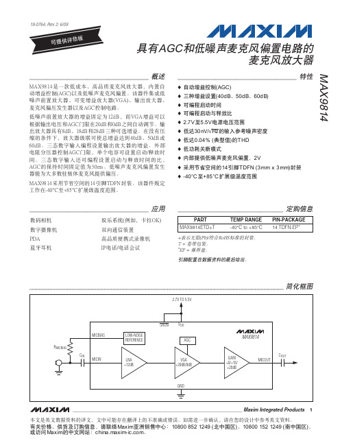
```````````````````````````````````গၤNBY:925ဵጙࢅ߅۾Ăອᒠ൱యज़हࡍLjดᒙᔈࣅᐐፄ఼ᒜ)BHD*ጲૺࢅᐅဉ൱యज़ມᒙăকୈૹ߅ࢅᐅဉ༄ᒙहࡍĂభܤᐐፄहࡍ)WHB*Ăၒ߲हࡍĂ൱యज़ມኹखညጲૺBHD఼ᒜ࢟വăࢅᐅဉ༄ᒙहࡍࡼᐐፄৼࢾᆐ23eCLjऎWHBᐐፄభጲোၒ߲࢟ኹਜ਼BHDඡሢᏴ31eCਜ਼1eCᒄମᔈࣅࢯஂăၒ߲हࡍᎌ9eCĂ29eCਜ਼39eCྯᒬభኡᐐፄăᏴᎌኹჁࡼᄟୈሆLjहࡍೊభဧᔐᐐፄࡉࡵ51eCĂ61eC71eCăྯზၫᔊၒྜྷܠ߈ᒙၒ߲हࡍࡼᐐፄăᅪݝ࢟ᔜॊኹ఼ᒜBHDඡሢLjৈ࢟ྏభᒙࣅ0ျहဟମăྯზၫᔊၒྜྷથభܠ߈ᒙࣅᎧျहဟମࡼ܈LjBHDࡼۣߒဟମৼࢾᒋᆐ41ntăࢅᐅဉ൱యज़ມᒙखညถᆐࡍࣶၫᓘᄏ൱యज़ᄋມኹăNBY:925ݧஂဏహମࡼ25୭UEGOॖᓤăকୈਖࢾᔫᏴ.51°Dᒗ,96°D౫ᐱᆨࣞपᆍă```````````````````````````````````።```````````````````````````````````ᄂቶ♦ᔈࣅᐐፄ఼ᒜ)BHD*♦ྯᒬᐐፄᒙ)51eCĂ61eCĂ71eC*♦భܠ߈ࣅဟମ♦భܠ߈ࣅᎧျह܈♦3/8Wᒗ6/6W࢟Ꮞ࢟ኹपᆍ♦ࢅࡉ41oW0√I{ࡼၒྜྷݬఠᐅဉමࣞ♦ࢅࡉ1/15&!)࢜ቯᒋ*ࡼUIE ♦ࢅਈࣥෝါ♦ดݝᄋࢅᐅဉ൱యज़ມᒙLj3W♦ݧஂဏహମࡼ25୭UEGO!)4nn!y!4nn*ॖᓤ♦.51°Dᒗ,96°D౫ᐱᆨࣞपᆍNBY:925ᎌBHDਜ਼ࢅᐅဉ൱యज़ມᒙ࢟വࡼ൱యज़हࡍ________________________________________________________________Maxim Integrated Products 1```````````````````````````````ࢾ৪ቧᇦ`````````````````````````````````````````````````````````````````````````````````଼છౖᅄ۾ᆪဵ፞ᆪၫᓾ೯ࡼፉᆪLjᆪᒦభถࡀᏴडፉࡼݙᓰཀྵࡇᇙăྙኊጙݛཀྵཱྀLj༿Ᏼิࡼଐᒦݬఠ፞ᆪᓾ೯ăᎌਈଥৃĂૡૺࢿ৪ቧᇦLj༿ೊNbyjnᒴሾ၉ᒦቦǖ21911!963!235:!)۱ᒦਪཌ*Lj21911!263!235:!)ฉᒦਪཌ*LjषᆰNbyjnࡼᒦᆪᆀᐶǖdijob/nbyjn.jd/dpnă+ܭာᇄ)Qc*0९SpITܪᓰࡼॖᓤăU!>!௳ࡒ۞ᓤă*FQ!>!ൡă୭ᒙᏴၫᓾ೯ࡼᔢઁ߲ăၫ൩ሤ૦ၫᔊስ૦QEB ౸ዀऐ૦Ꭵಘᇹᄻ)ಿྙLjఌ౯PL*ၷሶᄰቧᓤᒙອᒠܣቑါഺስ૦JQ࢟જ0࢟જ્ፇN B Y :925ᎌBHDਜ਼ࢅᐅဉ൱యज़ມᒙ࢟വࡼ൱యज़हࡍABSOLUTE MAXIMUM RATINGSELECTRICAL CHARACTERISTICS(V DD = 3.3V, SHDN = V DD , C CT = 470nF, C CG = 2μF, GAIN = V DD , T A = T MIN to T MAX , unless otherwise specified. Typical values are at T A = +25°C.) (Note 1)Stresses beyond those listed under “Absolute Maximum Ratings” may cause permanent damage to the device. These are stress ratings only, and functional operation of the device at these or any other conditions beyond those indicated in the operational sections of the specifications is not implied. Exposure to absolute maximum rating conditions for extended periods may affect device reliability.V DD to GND..............................................................-0.3V to +6V All Other Pins to GND.................................-0.3V to (V DD + 0.3V)Output Short-Circuit Duration.....................................Continuous Continuous Current (MICOUT, MICBIAS).......................±100mA All Other Pins....................................................................±20mAContinuous Power Dissipation (T A = +70°C)14-Pin TDFN-EP(derate 16.7mW/°C above +70°C)........................1481.5mW Operating Temperature Range ...........................-40°C to +85°C Junction Temperature......................................................+150°C Lead Temperature (soldering, 10s).................................+300°C Bump Temperature (soldering) Reflow............................+235°CNBY:925ᎌBHDਜ਼ࢅᐅဉ൱యज़ມᒙ࢟വࡼ൱యज़हࡍ_______________________________________________________________________________________3Note 1:Devices are production tested at T A = +25°C. Limits over temperature are guaranteed by design.Note 2:Dynamic range is calculated using the EIAJ method. The input is applied at -60dBFS (0.707μV RMS ), f IN = 1kHz.Note 3:Attack time measured as time from AGC trigger to gain reaching 90% of its final value.Note 4:CG is connected to an external DC voltage source, and adjusted until V MICOUT = 1.23V.Note 5:CG connected to GND with 2.2μF.ELECTRICAL CHARACTERISTICS (continued)(V DD = 3.3V, SHDN = V DD , C CT = 470nF, C CG = 2μF, GAIN = V DD , T A = T MIN to T MAX , unless otherwise specified. Typical values are at T = +25°C.) (Note 1)N B Y :925ᎌBHDਜ਼ࢅᐅဉ൱యज़ມᒙ࢟വࡼ൱యज़हࡍ4_______________________________________________________________________________________```````````````````````````````````````````````````````````````````````࢜ቯᔫᄂቶ(V DD = 5V, C CT = 470nF, C CG = 2.2μF, V TH = V MICBIAS x 0.4, GAIN = V DD (40dB), AGC disabled, no load, R L = 10k Ω, C OUT = 1μF,T A = +25°C, unless otherwise noted.)GAIN vs. FREQUENCYFREQUENCY (Hz)G A I N (d B )10k1k 1001020304050607080010100kPOWER-SUPPLY REJECTION RATIOvs. FREQUENCYFREQUENCY (Hz)P S R R (d B )10k1k 100-70-60-50-40-30-20-100-8010100kMICBIAS POWER-SUPPLY REJECTION RATIOvs. FREQUENCYFREQUENCY (Hz)P S R R (d B )10k1k 100-100-90-80-70-60-50-40-30-11010100kSUPPLY CURRENT vs. SUPPLY VOLTAGEM A X 9814 t o c 04SUPPLY VOLTAGE (V)S U P P L Y C U R R E N T (m A )5.55.04.04.53.53.02.62.72.82.93.03.13.23.33.43.52.52.56.0SHUTDOWN CURRENT vs. SUPPLY VOLTAGEM A X 9814 t o c 05SUPPLY VOLTAGE (V)S H U T D O W N C U R R E N T (n A )5.55.04.54.03.53.00.10.20.30.40.502.56.0MICROPHONE BIAS VOLTAGEvs. MICROPHONE BIAS SOURCE CURRENTM A X 9814 t o c 06I MICBIAS (mA)V M I C B I A S V O L T A G E (V )2520151050.51.01.52.02.50030TOTAL HARMONIC DISTORTION PLUS NOISEvs. FREQUENCYFREQUENCY (Hz)T H D +N (%)10k1k 1000.11100.0110100kTOTAL HARMONIC DISTORTION PLUS NOISEvs. OUTPUT VOLTAGEOUTPUT VOLTAGE (V RMS )T H D +N (%)1.00.50.11100.011.5INPUT-REFERRED NOISEvs. FREQUENCYFREQUENCY (kHz)I N P U T -R E F E R R E D N O I S E (μV R M S /√H z )1010.1100100.0110010001NBY:925ᎌBHDਜ਼ࢅᐅဉ൱యज़ມᒙ࢟വࡼ൱యज़हࡍ_______________________________________________________________________________________5MICBIAS NOISE vs. FREQUENCYMA X 9814 t o c 10FREQUENCY (Hz)M I C B I A S N O I S E(n V RM S /√H z )10k1k 100100100010,0001010100kSMALL-SIGNAL PULSE RESPONSE200μs/divV MICIN 10mV/div0VV MICOUT500mV/div0VTURN-ON RESPONSEM A X 9814 t o c 1220ms/divV SHDN 5V/div 0V V MICBIAS 2V/div 0VV MICOUT 1V/div 0VV OUT vs. V INV IN (mV RMS )V O U T (V R M S)100500.250.500.751.0000150V OUT vs. V INV IN (mV RMS )V O U T (V R M S)3020100.250.500.751.000040V OUT vs. V INV IN (mV RMS )V O U T (V R M S )1050.250.500.751.000015ATTACK TIME200μs/divV MICOUT 500mV/divC CT = 47nF0VATTACK TIME200μs/divV MICOUT 500mV/div0VHOLD AND RELEASE TIME20ms/divV MICOUT 500mV/divC CT = 47nF A/R = GND0V``````````````````````````````````````````````````````````````````````࢜ቯᔫᄂቶ)ኚ*(V DD = 5V, C CT = 470nF, C CG = 2.2μF, V TH = V MICBIAS x 0.4, GAIN = V DD (40dB), AGC disabled, no load, R L = 10k Ω, C OUT = 1μF,T A = +25°C, unless otherwise noted.)N B Y :925ᎌBHDਜ਼ࢅᐅဉ൱యज़ມᒙ࢟വࡼ൱యज़हࡍ6_______________________________________________________________________________________HOLD AND RELEASE TIME40ms/divV MICOUT 500mV/div0VHOLD AND RELEASE TIME100ms/divV MICOUT 500mV/div0V```````````````````````````````````````````````````````````````````````````````୭ႁී``````````````````````````````````````````````````````````````````````࢜ቯᔫᄂቶ)ኚ*(V DD = 5V, C CT = 470nF, C CG = 2.2μF, V TH = V MICBIAS x 0.4, GAIN = V DD (40dB), AGC disabled, no load, R L = 10k Ω, C OUT = 1μF,T A = +25°C, unless otherwise noted.)NBY:925ᎌBHDਜ਼ࢅᐅဉ൱యज़ມᒙ࢟വࡼ൱యज़हࡍ_______________________________________________________________________________________7MAX9814 AGC DISABLED400μs/div V MICIN 100mV/divV MICOUT(AC-COUPLED)1V/divMAX9814 fig01aMAX9814 AGC ENABLED400μs/divV MICIN 100mV/divV MICOUT(AC-COUPLED)1V/divMAX9814 fig01b0V0V0V0V```````````````````````````````ሮᇼႁීNBY:925ဵጙࢅ߅۾Ăອᒠ൱యज़हࡍLjดᒙᔈࣅᐐፄ఼ᒜ)BHD*ጲૺࢅᐅဉ൱యज़ມᒙăNBY:925ဵᎅࢅᐅဉ༄ᒙहࡍĂభܤᐐፄहࡍ)WHB*Ăၒ߲हࡍĂ൱యज़ມᒙखညጲૺBHD఼ᒜ࢟വࢀࣶৈݙᄴ࢟വᔝ߅ăดݝ൱యज़ມᒙखညᄋ3WࡼມኹLjး᎖ࡍࣶၫᓘᄏ࢟ྏါ൱యज़ăNBY:925ॊᆐྯLj࣪ၒྜྷቲहࡍăᏴጙLjၒྜྷᄰਭᐐፄᆐ23eCࡼࢅᐅဉ༄ᒙहࡍቲદߡਜ਼हࡍǗऔᐌᎅBHD఼ᒜࡼWHBᔝ߅LjWHB0BHDᔝถ৫ဧᐐፄᏴ31eCᎧ1eCᒄମܤછǗၒ߲हࡍဵᔢઁጙLjᎌ9eCĂ29eCĂ31eCྯৈݙᄴࡼৼࢾᐐፄLjభᄰਭጙৈྯზ൝ၒྜྷܠ߈ᒙăBHDᇄኹჁဟLjNBY:925ถ৫ᄋ51eCĂ61eC71eCࡼᐐፄăᔈࣅᐐፄ఼ᒜ)BHD*ݙ۸BHDࡼୈᏴၒྜྷᐐፄਭࡍဟLjၒ્߲߲ሚሻ݆ǗऎᏴၒྜྷᐐፄਭࡍဟLjBHDถ৫ܜၒ߲ሻ݆ăᅄ2Ⴥာᆐᐐፄਭࡍࡼ൱యज़ၒྜྷᏴᎌBHDਜ਼ݙࡒBHDࡼ༽ౚሆࡼ܈୷ăNBY:925ࡼBHD࣪ᐐፄቲ఼ᒜLj၅ሌଶހၒ߲࢟ኹဵ॥ިਭᎾඡሢăႲઁLjᄰਭభኡࡼဟମޟၫଢ଼ࢅ൱యज़हࡍᐐፄLjጲኀᑵਭࡍࡼၒ߲࢟ኹ७ᒋăᑚጙਭ߈߂ᆐࣅဟମăࡩၒ߲ቧ७ᒋଢ଼ࢅઁLjᐐፄᏴ੪ဟମดۣߒၱିᓨზLjႲઁၒ߲ቧદൻᐐଝࡵᑵޟᒋăকਭ߈߂ᆐۣߒਜ਼ျहဟମăहࡍࢯஂၒྜྷቧࡼႥࣞᎅᅪݝࢾဟ࢟ྏD DU ਜ਼B0S࣡࢟ኹᒙăBHDඡሢభᄰਭW UI ࢯஂăᐐፄၱିᆐၒྜྷቧ७ᒋࡼၫLjᔢࡍBHDၱିᆐ31eCăᅄ3߲೫ၒྜྷᅃި߲ᎾඡሢဟLj࣪ၒ߲ࣅဟମĂۣߒဟମਜ਼ျहဟମࡼ፬ሰăྙਫᒙࡼࣅဟମਜ਼ျहဟମሰ።ვLjᐐፄႲቧࣅზܤછऎႥࢯஂLjޟޟ્ޘညಢ႒Đກđဉ)qvnqjoh*Đࠇᇦđဉ)csfbuijoh*ࡼፒຫᐅဉăࢯஂBHDࡼဟମޟၫဧᎧဉᏎປLj࠭ऎࡉࡵᔢଛਫă࣪᎖กቋጲDEፒಘᆐᓍገፒᏎࡼ።ႁLjᅎୀࣅဟମᆐ271μtLjျहဟମᆐ91ntăᄰޟ༽ౚሆLjፒಘ݃ह۸ገ܈Ꭻፒ࢟፬ࢀ۸ኊገৎࡼျहဟମăᅄ2/!ࡒᎌBHDਜ਼ᎌBHDࡼ൱యज़ၒྜྷࣅဟମࣅဟମဵᒎࡩၒྜྷቧިਭඡሢ࢟ຳઁLjBHDଢ଼ࢅᐐፄჅኊࡼဟମăᐐፄᏴࣅဟମดጲᒎၫተါၱିLjࢾፃᆐጙৈဟମޟၫăকဟମޟၫᆐ3511y D DU )ᒦD DU ဵᅪݝࢾဟ࢟ྏ*ǖ•ኡན୷ࡼࣅဟମLjጲۣᑺBHDႥሰ።ၾზቧLjಿྙૣ৴ဉ)ፒಘ*།ૣဉ)EWE*ă•ኡ୷ޠࡼࣅဟମLjBHDၾဟख़ᒋLjᒑᎌࡩဉሰීመᐐଝဟݣଢ଼ࢅᐐፄăၾဟख़ᒋ݀ݙۻၱିLjࡣ୷ሰࡼဉፒۻၱିăᑚዹభ࠭ፒଢ଼ࢅሰဉLjဧࣅზपᆍᔢࡍછăۣߒဟମۣߒဟମဵᒎቧଢ଼ࡵඡሢጲሆĂျहਭ߈ఎဪጲ༄ࡼዓߕăۣߒဟମดݝᒙᆐ41ntLj݀༦ݙభࢯăࡩቧިਭඡሢLjᒮቤྜྷࣅࣤဟLjۣߒဟମᒫᒏăျहဟମျहဟମဵᒎቧࢰൢᒗඡሢጲሆLj݀༦ளਭ41ntࡼۣߒဟମᒄઁLjᐐፄૄࡵᑵޟၺຳჅኊࡼဟମăျहဟମࢾፃᆐࡩၒྜྷቧࢰൢᒗUIඡሢጲሆLj݀༦ளਭ41nt ࡼۣߒဟମᒄઁLjᐐፄ࠭31eCኹჁျहࡵᑵޟᐐፄࡼ21&ࡼဟମăျहဟମభࢯLjᔢቃᒋᆐ36ntăျहဟମᎅD DU ᒙࡼࣅဟମጲૺಽB0S )ྙܭ2Ⴥာ*ᒙࡼࣅ0ျहဟମ܈ཀྵࢾǖ•ݧቃ܈ᒋLjဧBHDࡼႥࣞࡉࡵᔢࡍă•ݧࡍ܈ᒋLjဧፒᒠࡉࡵᔢଛLjऴᒏBHDᒮআࢯஂဟମดި߲ඡሢࡼቧăBHDၒ߲ඡሢ૮BHDᔫࡼၒ߲ඡሢభᄰਭᅪݝ࢟ᔜॊኹࢯஂăᅲ߅࣪ॊኹࡼᒙઁLjBHDଢ଼ࢅᐐፄLjဧၒ߲࢟ኹᎧUIၒྜྷ࣡ᒙࡼ࢟ኹሤປă൱యज़ມᒙNBY:925ᎅดݝᄋࢅᐅဉ൱యज़ມᒙ࢟ኹLjభདࣅࡍࣶၫᓘᄏ࢟ྏါ൱యज़ăࢯஂ൱యज़ມᒙᒗ3WLjጲۣᑺྜྷࢅᐅဉ༄ᒙहࡍࡼၒྜྷቧݙۻὥᆡࡵă```````````````````````````````።ቧᇦᒙࣅဟମਜ਼ျहဟମࣅဟମਜ਼ျहဟମॊܰᎅDUਜ਼HOEᒄମࡼ࢟ྏጲૺB0Sࡼ൝ᓨზ)ܭ2*ࢾăB0Sᆐྯზ൝ၒྜྷLjభᒙࣅᎧျहဟମ܈ăোܭ3Ⴥࡼሤ።࢟ྏLjభጲኡᐋࣅဟମਜ਼ျहဟମăN B Y :925ᎌBHDਜ਼ࢅᐅဉ൱యज़ມᒙ࢟വࡼ൱యज़हࡍ8_______________________________________________________________________________________10ms/divATTACKRELEASEHOLDᅄ3/!ၒྜྷᅃިਭBHDඡሢܭ2/!ࣅᎧျह܈ܭ3/!ࣅ.ျहဟମᒙBHDඡሢྦገᒙ൱యज़ၒ߲ὥᆡဟࡼၒ߲࢟ኹඡሢLj።ᏴNJDCJBTਜ਼ᒄମೌᅪݝ࢟ᔜॊኹLj࢟ᔜॊኹၒ߲ೌࡵUIă࢟ኹW UIభཀྵࢾၒ߲ὥᆡဟࡼख़ᒋ࢟ኹඡሢăࠥဟLjၒ߲࣡ࡼᔢࡍቧڼ७ᆐW UIࡼ3۶Ljۣ݀ߒݙܤLjᒇࡵၒྜྷቧ७ᒋၱିᆐᒏăྦገணᒏBHDLjభUIೌᒗNJDCJBTă൱యज़ມᒙ࢟ᔜNJDCJBTభᏎ߲31nBࡼ࢟ഗăኡᐋးࡩࡼS NJDCJBTLj࠭ऎᆐᓘᄏ൱యज़ᄋჅኊገࡼມᒙ࢟ഗăጙۅႁLj3/3lΩࡼᔜᒋ࣪᎖࢜ቯഉැࣞࡼ൱యज़ጯளᔗ৫೫ăਈ᎖ມᒙ࢟ᔜࡼኡᐋLj༿ݬఠ൱యज़ၫᓾ೯ăມᒙ࢟ྏNBY:925ࡼCJBTၒ߲ᏴดݝளਭદߡLjᄋࢅᐅဉມኹăݧጙᒑ581oGࡼ࢟ྏCJBTവᒗăၒྜྷ࢟ྏ൱యज़हࡍࡼၒྜྷୣഗẮ࢟ྏ)D JO*ਜ਼ၒྜྷᔜఝ)S JO*ᔝ߅೫ጙৈᄰ݆Ljభ߹ၒྜྷቧᒦࡼჅᎌᒇഗມᒙ)ݬ࢜ቯ።࢟വ0ถౖᅄ*ăD JOభऴᒏၒྜྷቧᏎࡼᒇഗ߅ॊ߲ሚᏴहࡍࡼၒ߲ăଣၒྜྷቧᏎᔜఝᆐഃLjᐌᄰ݆ࡼ.4eC࢛ᆐǖኡᐋးࡩࡼD JOဧg.4eC`JOᏐࢅ᎖ැঢຫൈăg.4eC`JOᒙਭLj્፬ሰहࡍࡼࢅຫሰ።Ljኡᐋࢅ࢟ኹᇹၫࡼ࢟ᒠ࢟ྏă࣪᎖ୣഗẮ࢟ྏႁLjി࢟ஊ࢟ྏĂᶉ࢟ྏۡෞ࢟ᒠ࢟ྏ࣒ဵ੪ੑࡼኡᐋă࢟ኹᇹၫࡼ࢟ྏLjᓄྙჿࠣ࢟ྏ)ऻD1H࢟ᒠ*Lj્ଝ௭ࢅຫပᑞăၒ߲࢟ྏNBY:925ࡼၒ߲ມᒙᏴ2/34WLjྦገሿ߹ᒇഗပࢯLj።ݧୣഗẮ࢟ྏ)D PVU*ăఠࡵሆጙࡼၒྜྷᔜఝ)S M*LjD PVUਜ਼S Mᔝ߅ᄰ݆ăଣၒ߲ᔜఝᆐഃLjᄰ݆ࡼ.4eC࢛ᆐǖਈࣥNBY:925ᎌࢅਈࣥෝါăࡩSHDNᆐࢅ࢟ຳဟLj࢟Ꮞ࢟ഗࢰൢᒗ1/12μBLjၒ߲ྜྷᔜᓨზLj൱యज़ࡼມᒙ࢟ഗਈࣥăདࣅSHDNᆐ࢟ຳLjဧถहࡍă༿ᇖSHDNኞహă࢟ᏎവᎧQDCݚݧጙᒑ1/2μGࡼ࢟ྏ࢟ᏎവᒗăჁሣޠࣞభଢ଼ࢅည࢟ྏLjᅪݝᏄୈ።భถణதୈहᒙLjᅎୀኡܭᄣᏄୈăᏴᄴဟᎌෝผਜ਼ၫᔊࡼᇹᄻᒦLjNBY:925ࡼᎧෝผሤೌăNBY:925ᎌBHDਜ਼ࢅᐅဉ൱యज़ມᒙ࢟വࡼ൱యज़हࡍ_______________________________________________________________________________________9N B Y :925ᎌBHDਜ਼ࢅᐅဉ൱యज़ມᒙ࢟വࡼ൱యज़हࡍ10______________________________________________________________________________________```````````````````````````````````````````````````````````````````࢜ቯ።࢟വ0ถౖᅄNBY:925൱యज़हࡍ______________________________________________________________________________________11`````````````````````````````````በຢቧᇦPROCESS: BiCMOS`````````````````````````````````୭ᒙN B Y :925൱యज़हࡍ12______________________________________________________________________________________`````````````````````````````````````````````````````````````````````````````ॖᓤቧᇦྙኊᔢதࡼॖᓤᅪተቧᇦਜ਼ݚLj༿އኯ/packages ăNBY:925൱యज़हࡍ______________________________________________________________________________________13````````````````````````````````````````````````````````````````````````````````ॖᓤቧᇦ)ኚ*ྙኊᔢதࡼॖᓤᅪተቧᇦਜ਼ݚLj༿އኯ/packages ăN B Y :925൱యज़हࡍ````````````````````````````````````````````````````````````````````````````ኀࢿ಼ဥNbyjnݙ࣪Nbyjnޘອጲᅪࡼྀੜ࢟വဧঌᐊLjጐݙᄋᓜಽభăNbyjnۣഔᏴྀੜဟମĂᎌྀੜᄰۨࡼ༄ᄋሆኀখޘອᓾ೯ਜ਼ਖৃࡼཚಽă14____________________Maxim Integrated Products, 120 San Gabriel Drive, Sunnyvale, CA 94086 408-737-7600©2009 Maxim Integrated ProductsNbyjn ဵNbyjn!Joufhsbufe!Qspevdut-!Jod/ࡼᓖݿܪăNbyjn ۱யێူࠀ۱ய9439ቧረᎆᑶܠ൩211194ॅ࢟જǖ911!921!1421࢟જǖ121.732262::ࠅᑞǖ121.732263::。
- 1、下载文档前请自行甄别文档内容的完整性,平台不提供额外的编辑、内容补充、找答案等附加服务。
- 2、"仅部分预览"的文档,不可在线预览部分如存在完整性等问题,可反馈申请退款(可完整预览的文档不适用该条件!)。
- 3、如文档侵犯您的权益,请联系客服反馈,我们会尽快为您处理(人工客服工作时间:9:00-18:30)。
o 12-Bit Resolution, ±0.5 LSB Linearity o Single +5V Operation o Internal +2.5V Reference o Software-Configurable Analog Input Multiplexer 6-Channel Single-Ended/ 3-Channel Pseudo-Differential (MAX1294) 2-Channel Single-Ended/ 1-Channel Pseudo-Differential (MAX1296) o Software-Configurable Unipolar/Bipolar Analog Inputs o Low Current 2.8mA (420ksps) 1.0mA (100ksps) 400µA (10ksps) 2µA (Shutdown) o Internal 6MHz Full-Power Bandwidth Track/Hold o Parallel 12-Bit Interface o Small Footprint 28-Pin QSOP (MAX1294) 24-Pin QSOP (MAX1296)
元器件交易网
420ksps, +5V, 6-/2-Channel, 12-Bit ADCs with +2.5V Reference and Parallel Interface MAX1294/MAX1296
ABSOLUTE MAXIMUM RATINGS
VDD to GND ..............................................................-0.3V to +6V CH0–CH5, COM to GND ............................-0.3V to (VDD + 0.3V) REF, REFADJ to GND.................................-0.3V to (VDD + 0.3V) Digital Inputs to GND ...............................................-0.3V to +6V Digital Outputs (D0–D11, INT) to GND.......-0.3V to (VDD + 0.3V) Continuous Power Dissipation (TA = +70°C) 24-Pin QSOP (derate 9.5mW/°C above +70°C)..........762mW 28-Pin QSOP (derate 8.00mW/°C above +70°C)........667mW Operating Temperature Ranges MAX1294_C_ _/MAX1296_C_ _ .........................0°C to +70°C MAX1294_E_ _/MAX1296_E_ _ ......................-40°C to +85°C Storage Temperature Range .............................-65°C to +150°C Lead Temperature (soldering, 10s) .................................+300°C
ELECTRICAL CHARACTERISTICS
(VDD = +5V ±10%, COM = GND, REFADJ = VDD, VREF = +2.5V, 4.7µF capacitor at REF pin, fCLK = 7.6MHz (50% duty cycle), TA = TMIN to TMAX, unless otherwise noted. Typical values are at TA = +25°C.) PARAMETER DC ACCURACY (Note 1) Resolution Relative Accuracy (Note 2) Differential Nonlinearity Offset Error Gain Error (Note 3) Gain Temperature Coefficient Channel-to-Channel Offset Matching Signal-to-Noise Plus Distortion Total Harmonic Distortion (including 5th-order harmonic) Spurious-Free Dynamic Range Intermodulation Distortion Channel-to-Channel Crosstalk Full-Linear Bandwidth Full-Power Bandwidth CONVERSION RATE External clock mode Conversion Time (Note 5) T/H Acquisition Time Aperture Delay Aperture Jitter External Clock Frequency Duty Cycle 2 fCLK tCONV tACQ External acquisition or external clock mode External acquisition or external clock mode Internal acquisition/internal clock mode 0.1 30 25 <50 <200 7.6 70 External acquisition/internal clock mode Internal acquisition/internal clock mode 2.1 2.5 3.2 3.0 3.6 3.5 4 400 ns ns ps MHz % µs SINAD THD SFDR IMD fIN1 = 49kHz, fIN2 = 52kHz fIN = 175kHz (Note 4) SINAD > 68dB -3dB rolloff -80 76 -78 350 6 67 ±2.0 ±0.2 RES INL DNL MAX129_A MAX129_B No missing codes over temperature 12 ±0.5 ±1 ±1 ±4 ±4 Bits LSB LSB LSB LSB ppm/°C LSB SYMBOL CONDITIONS MIN TYP MAX UNITS
19 GND 18 COM 17 CH0 16 CH1 15 CS 14 CLK 13 WR
D2 8 D1 9 D0 10 INT 11 RD 12
QSOP Pin Configurations continued at end of data sheet. Typical Operating Circuits appear at end of data sheet.
MAX1296AEEG -40°C to +85°C MAX1296BEEG -40°C to +85°C
________________________________________________________________ Maxim Integrated Products
1
For pricing, delivery, and ordering information, please contact Maxim/Dallas Direct! at 1-888-629-4642, or visit Maxim’s website at .
MAX1296
Ordering Information
PART MAX1294ACEI MAX1294BCEI MAX1294AEEI MAX1294BEEI MAX1296ACEG MAX1296BCEG TEMP RANGE 0°C to +70°C 0°C to +70°C -40°C to +85°C -40°C to +85°C 0°C to +70°C 0°C to +70°C PIN-PACKAGE 28 QSOP 28 QSOP 28 QSOP 28 QSOP 24 QSOP 24 QSOP 24 QSOP 24 QSOP INL (LSB) ±0.5 ±1 ±0.5 ±1 ±0.5 ±1 ±0.5 ±1
Pin Configurations
TOP VIEW
D9 1 D8 2 D7 3 D6 4 D5 5 D4 6 D3 7 24 D10 23 D11 22 VDD 21 REF 20 REFADJ
Applications
Industrial Control Systems Energy Management Data-Acquisition Systems Data Logging Patient Monitoring Touchscreens
元器件交易网
19-1533; Rev 2; 12/02
KIT ATION EVAksps, +5V, 6-/2-Channel, 12-Bit ADCs with +2.5V Reference and Parallel Interface
Stresses beyond those listed under “Absolute Maximum Ratings” may cause permanent damage to the device. These are stress ratings only, and functional operation of the device at these or any other conditions beyond those indicated in the operational sections of the specifications is not implied. Exposure to absolute maximum rating conditions for extended periods may affect device reliability.