Conductance of a quantum point contact based on spin-density-functional theory
第一届凝聚态物理会议

第一届凝聚态物理会议The 1st Conference on Condensed Matter Physics2015年7月15日- 17日清华大学目录01 会议概况02 组织委员会04 会议日程•总日程•大会报告•分会场报告•海报会场会议概况为了配合凝聚态物理在中国的迅速发展和国际地位的全面提升,进一步加强国内科研工作者在不同前沿领域的交流,推进国内和国际在凝聚态物理领域的相互交流和合作,为青年学生和研究人员学习和了解国际前沿进展创造更广泛的交流平台,拟定在过去已经成功举办了13届的“凝聚态理论与材料计算国际会议”系列会议的基础上,拓宽会议的主题,特别是加强凝聚态物理实验和理论的交流与融合,于2015年7月15日-17日在北京举办“第一届凝聚态物理会议”年会。
2015年第一届凝聚态物理会议是由清华大学物理系、中国科学院物理研究所、北京大学物理学院、量子物质科学协同创新中心联合主办。
这是国内首次在凝聚态物理方面举办的大型学术交流会。
本次会议是凝聚态理论与材料计算国际会议的延续和拓展,旨在增进国内外物理学者的学术交流,分享前沿科研成果,提高国内凝聚态物理的科研水平,扩大学术声誉。
第一届凝聚态物理会议将于2015年7月15日-17日在清华大学举行。
会议主题包括:拓扑量子态和多铁性、超导和多体物理、能源和低维物理、Quantum many-body theory and statistical physics、计算凝聚态物理、量子信息及其它与凝聚态物理的交叉领域等六个主题。
本次会议共设30个专题分会,将以大会特邀报告、分会特邀报告、口头报告和张贴海报等形式进行交流探讨。
组织委员会主办单位•清华大学物理系•中国科学院物理研究所•北京大学物理学院•量子物质科学协同创新中心顾问委员会:(按姓氏拼音序)崔田、杜瑞瑞、冯世平、龚新高、解士杰、李东海、李建新、林海青、李树深、陆卫、卢仲毅、吕力、沈保根、沈健、沈志勋、苏刚、王恩哥、王孝群、王玉鹏、向涛、薛其坤、张富春、张振宇组织委员会•清华大学物理系:陈曦、薛其坤•中科院物理研究所:胡江平、戴希、方忠、丁洪、周兴江、向涛•北京大学物理学院:谢心澄分会场负责人•拓扑量子态和多铁性:胡江平、陈曦、吕力、戴希、翁红明、寇谡鹏、吴从军•超导和多体物理:孙力玲、杨义峰、刘俊明、雒建林、袁辉球、李永庆、万歆、周毅•能源和低维物理:张振宇、李泓、陈弘、赵怀周、张远波•Quantum many-body theory and statistical physics:孟子扬、张广铭、郭文安、姚宏•计算凝聚态物理:姚裕贵、段文晖、龚新高、孟胜•量子信息及其它与凝聚态物理的交叉领域:范珩、田琳、翟荟、崔晓玲会议协调人•清华大学物理系:任俊(总协调人)•中国科学院物理研究所:齐建为、刘青梅•会务组:黄文艳、唐林、井小苏、周丹、骆洁、甘翠云、付德永、杨红、肖琳、胡文婷赞助单位•清华大学物理系•量子物质科学协同创新中心•中国科学院物理研究所•北京大学物理学院2015年第一届凝聚态物理会议分会场主题:A.拓扑量子态和多铁性A1拓扑半金属IA2拓扑半金属IIA3拓扑超导体和Majorana 费米子A4多铁性材料模拟与计算A5多铁性体系B.超导和多体物理B1铬基和锰基超导体B2极端条件下的超导行为B3铁基超导B4凝聚物质的激发态和动力学理论和实验B5重费米子物理C.能源和低维物理C1锂电池中的物理C2二维材料C3二维电子系统中的物理C4硅烯的最新进展C5热电中的新物理D.Quantum many-body theory and statistical physicsD1 Recent developments in strongly correlated quantum systems ID2 Recent developments in strongly correlated quantum systems IID3 Recent developments in strongly correlated quantum systems IIID4 Recent developments in strongly correlated quantum systems IVD5 Recent developments in strongly correlated quantum systems V注意事项:为了尊重外籍邀请报告人,如无特殊情况,D分会场报告请用英文。
Chemical principles of single-molecule(单分子的化学原理)

Over the past century, experimental physicists and engineers have developed sophisticated methods to create semiconducting silicon-based devices, such as diodes, transistors and memory elements, of increas-ingly small dimensions. Meanwhile, chemists have acquired a detailed understanding of the relationship between the chemical structure and the electronic properties of a molecule through reaction chemistry, advanced physical chemistry and theoretical methods. These multidisciplinary efforts have converged in the field of single-molecule electronics (SMEs), in which the ultimate goal is to use molecules as active elements in electronic circuitry1,2. A rich knowledge base detail-ing the electronic properties of molecules already exists in the context of chemical reactivity; reimagining such properties in the framework of SMEs might then inspire tremendous advancements in the field.Powerful methods have been developed to charac-terize and manipulate the conductance properties of single molecules3–6. Molecular conductance has been measured using techniques based on scanning tunnel-ling microscopy (STM)7, mechanically controlled break junctions8–11, STM break junctions12,13, conductive atomic force microscopy14, electromigration15, nanoparticle arrays16,17 and other approaches18–21. The sophistication of these techniques provides the opportunity for chemists to collaborate with physicists and engineers to incorporate well-understood chemical principles into the study of structure–conductivity relationships in molecular wires.Reviews on SMEs are usually written from the per-spective of those who build devices and measure their properties — the link between chemistry and SME devices is rarely the focus. Filling this gap will address the questions that arise from the expanding structural diversity of molecular wires in the SME literature. For example, how will the single-molecule conduct-ance paradigm, which was first developed for simple molecular structures, shift as molecular wires grow in structural complexity and diversity? Which lessons can be drawn from reaction chemistry to guide the design of molecular electronics? How can chemical expertise be used to engineer new functions into single-molecule wires?In this Review, we integrate the languages of chemis-try and device physics to explain the chemical concepts that underlie single-molecule conductance. We discuss the structure–property relationships of single-molecule junctions by deconstructing the junction into three distinct components: the anchor, the electrode and the bridge (FIG. 1). We survey the modularity of each component and describe how tuning the structure of each part affects the charge-transport properties of the junction, primarily in the context of break-junction experiments. Finally, we examine emerging areas in SME research, such as single-molecule conductance switches and quantum interference (QI), and discuss how these are fundamentally related to well-established chemical principles.1Department of Chemistry, Columbia University.2Department of Physics and Applied Math, Columbia University, New York,New York 10027, USA. Correspondence to M.L.S., L.V. and C.N.mls2064@;lv2117@;cn37@Arricle number: 16002doi:10.1038/natrevmats.2016.2 Published online 23 Feb 2016Chemical principles of single-molecule electronicsTimothy A. Su1, Madhav Neupane1, Michael L. Steigerwald1, Latha Venkataraman1,2and Colin Nuckolls1Abstract | The field of single-molecule electronics harnesses expertise from engineering, physics and chemistry to realize circuit elements at the limit of miniaturization; it is a subfield of nanoelectronics in which the electronic components are single molecules. In this Review, we survey the field from a chemical perspective and discuss the structure–property relationships of the three components that form a single-molecule junction: the anchor, the electrode and the molecular bridge. The spatial orientation and electronic coupling between each component profoundly affect the conductance properties and functions of thesingle-molecule device. We describe the design principles of the anchor group, the influence of the electronic configuration of the electrode and the effect of manipulating the structure of the molecular backbone and of its substituent groups. We discuss single-molecule conductance switches as well as the phenomenon of quantum interference and then trace their fundamental roots back to chemical principles.REVIEWSAnchor groupThe anchor group (also known as the linker or contact group) connects the molecular wire to the electrodes both mechanically and electronically. Usually, a single anchoring group terminates each end of the molecule to form the metal–molecule–metal junction; however, including more anchoring units along the molecular bridge can offer additional handles for tuning con-ductance, depending on which two anchors form the most conductive pathway 22–27. Anchoring groups typi-cally bind to electrodes either through donor–acceptor (dative) interactions or through covalent bonding. Prototypical anchor groups for each type of electrode–linker interaction are shown in FIG. 2a . Because gold is the most used electrode material in SME studies, we focus primarily on the interaction of anchor groups with gold electrodes.Dative interactions involve the electron donation from a π donor or a lone pair donor to a Lewis acidic Au atom. Common π donors include fullerenes 28,29 and other π-conjugated hydrocarbons 19,26,30,31. Many lone pair anchoring groups are common σ-donor ligands familiar from coordination chemistry 32. Dative con-tacts, such as amines, are advantageous because they bind selectively to undercoordinated adatoms on the electrode surface; this narrows the conductance distri-bution because it limits the Au–linker contact geom-etry 33. Covalent contacts between the metal and the molecule result from covalent bonding between mole-cular radicals and metallic electrode surfaces. Covalent contacts are valuable because they are physically robust linkages that strongly couple the electronics of the molecule and the metal.Conductance depends not only on the class of the anchoring group but also on the nature of the inter-action between the anchor group and the other com-ponents of the junction — that is, the bridge and the electrode. In the following sections, we explore how the spatial overlap between the orbitals of these three components affects the charge-transport properties of the junction.Before we continue, we must clarify the meaning of the conductance values that are discussed. There is significant measurement-to-measurement variability in single-molecule experiments that is due to fluctuations in the molecular conformation, the electrode–anchor contact geometry and the electrode surface geometry. To account for this variability and to better under-stand the nature of conductance in a single molecule,researchers analyse hundreds to thousands of measure-ment traces together by compiling them into conduct-ance histograms to obtain a distribution of all measured conductance values. The conductance values that we report here refer to the conductance peak values from such histograms reported in units of G 0. G 0 is the con-ductance quantum and is defined as G 0 = 2e 2/h = 77.5 μS, where e is the charge of an electron and h is Planck’s constant; it is the preferred unit used to describe the conductance between metal point contacts as well as molecular conductance.Effect of anchor–bridge orbital overlap on conductance. The anchor group often dictates whether the mole c ular wire transports holes (highest occupied molecular orbital (HOMO)-dominated conductance) or elec-trons (lowest unoccupied molecular orbital (LUMO)-dominated conductance). The dominant conducting molecular orbital is typically the orbital that is closest in energy to the electrode Fermi level, E F . Conductance depends on the energy offset, ΔE , between E F and the conducting orbital, and on the strength of the elec-trode–molecule hybridization, Γ (BOX 1). The nature of the conducting orbital can be determined experimen-tally through thermopower measurements 34,35 or com-putationally by transmission calculations 36. However, in simple structures, we can predict the nature of charge carriers from basic chemical principles by considering the nature of the molecular backbone and the geome-try of the lone pair relative to the conjugated orbitals of the molecule (FIG. 2b). To illustrate this method, we use a phenyl ring terminated at the para positions by the dative linker groups from FIG. 2a . This analysis can be applied to other basic aromatic wires as well. For ben-zene rings terminated with linkers such as –SR, –NH 2, –PR 2 or –SeR at the 1,4-positions, the lone pair orbitals are included in the HOMO because they are coplanar with and energetically destabilized by the filled π-con-jugated bridge orbitals. Thus, owing to the alignment of the Au–lone pair bonds with the π system of the bridge, conductance occurs strongly through the HOMO when such anchor groups are used.By contrast, conductance in phenyl rings terminated by pyridine 37, isocyanide 38 and cyanide 39 linkers occurs primarily through the LUMO. For these anchor groups, the lone pair lies in the σ plane of the molecule, rigidly orthogonal to the π channel of the wire. Conduction through the lone pair orbitals is weak because the car-bon sp 2 σ orbitals are poorly conjugated 40. Moreover, the lone pair orbital is generally quite low in energy because it is part of the σ system; thus, transport through this orbital has a marginal contribution to conductance (ΔE is large). Just as importantly, the elec-tron-withdrawing nature of these linker groups facili-tates LUMO-dominated conductance by lowering the energy of the π*-antibonding orbitals towards the E F (and the HOMO-conducting π-bonding orbitals away from the E F ). The conductance is then controlled by the coupling between the electrodes and the π*-antibond-ing orbitals of the LUMO. When molecular bridges are very electron-deficient structures, such as thiophene| Materials Figure 1 | A schematic of a single-molecule junction with electrode, anchor and bridge components. The bridge unit can be further deconstructed into backbone (blue block) and substituent (red circles) subunits. I , current.dioxides 41 and porphyrins 42, in which the HOMO and LUMO energies are substantially lowered, conductance through the LUMO can dominate regardless of the type of linker used.HOMO and LUMO conduction can also be understood from the perspective of coordination chemistry and of the different modes of interaction between ligands and transition metals. Hole trans-port or HOMO-dominated conduction occurs when the metal–molecule bond, formed using the σ-donor orbital of the molecule (which in most cases is the HOMO of the isolated molecule) and the σ-accepting orbital of the metal, can become coplanar with the con-jugated bridge orbitals. This coplanarity ensures that the metal–molecule bond, the ‘gateway’, can mix with the delocalized, conjugated bridge orbitals and estab-lish the conductivity path. Conversely, if the metal- to-molecule σ bond cannot mix with the conjugated pathway, the charge carriers cannot use the molecular HOMO; it is geometrically unavailable and energet-ically distant from the E F . However, it is well known from coordination and organometallic chemistry that although ligand-to-metal σ donation usually dominates metal–ligand bonding, it is often supplemented by d metal to π*ligand ‘back-bonding’, in which occupied orbit-als of the metal mix with unoccupied orbitals of theligand. In the case of molecular conduction, when the σ-donation (HOMO-transporting) pathway is un a vail-able, this π* back-bonding (LUMO-transporting) path-way may be available if the π* orbital, into which the metal back- d onates, is a conjugated orbital that spans the molecule and is connected to both electrodes.The stereochemistry of the Au–anchor bond with respect to the conductive channel of the molecular bridge determines the strength of the electronic cou-pling between the metal and the molecule; manipulating this stereochemistry is a powerful handle for controlling conductance. The charge flow between the electrodes increases if the Au–anchor bond is aligned with the con-jugated orbitals of the molecule. The position of sulfur lone pairs can be locked into alignment with the molec-ular π backbone using a dihydrobenzothiophene (BT) thioether linker 43. The frustrated rotation of the S lone pair results in increased conductance and in a sharper conductance peak compared with analogous aromatic wires with thiomethyl linkers that can freely rotate. The BT linker has been incorporated into several dif-ferent molecular wires to strengthen the anchor–bridge coupling 27,44–46.Poor coupling between the electrode and the mole c ule can also be a desirable quality. Electrode– molecule coupling can be disrupted by insertingNature Reviews | Materials abH 2N-Ph-NH 2(HOMO)NC-Ph-CN (HOMO-2)NC-Ph-CN (LUMO)Figure 2 | Anchor group archetypes and the nature of charge carriers for common dative anchors. a | Molecularstructures of common anchors. Dative anchors can be classified as π donating or lone pair donating. For lone pair donors, the anchors shown in the left and in the right columns impart lowest unoccupied molecular orbital (LUMO)- and highest occupied molecular orbital (HOMO)-dominated conductance, respectively, in simple π-conjugated systems. Covalent anchors commonly used to generate direct Au–S and Au–C contacts are shown in the last column. These contacts can be generated from thiol oxidation, Au–Sn transmetalation, fluoride-initiated desilylation and diazonium electroreduction reactions. b | The highest energy molecular orbital surfaces that feature strong lone pair character are depicted for 1,4-diaminobenzene (left panel) and 1,4-dicyanobenzene (middle panel) (B3LYP/6-31G**). In 1,4-diaminobenzene, the N-centred lone pairs occupy p orbitals that, like the benzene π orbitals, are perpendicular to the plane of the ring. In 1,4-dicyanobenzene, these N-centred lone pair orbitals are orthogonal to the π channel of the benzene ring; conductance in this system is dominated instead by transport through the LUMO (right panel).R E V I E W Smethylene (CH2) units between the S atom and the phenyl ring. The methylene spacers allow gating effects, such as Coulomb blockade, to occur in three-electrode systems because they decouple the molecule from the source and drain the electrodes47(FIG. 3a). However, the reduction in molecule–electrode coupling has been shown to decrease the junction conductance by three orders of magnitude in π-conjugated molecules47. Interesting functions can be implemented into molec-ular electronic devices by synthetically engineering anchor groups with both strong and weak electrode–molecule coupling character. A bulky –SPh anchor group can be used to misalign the S–Au bond with the molecular bridge, decreasing the molecule–electrode coupling45. This enables the creation of a single-mole-cule rectifier, whereby the molecule is strongly coupled to the electrode by a covalent Au–C bond at one end and weakly coupled by a Au–SPhR bond at the other end. A class of oligosilanes and oligogermanes that switch between different conductance values depending on the strength of the coupling between the electrode and the molecule has recently been described48,49. Junction elongation stretches the terminal ends of the molecule into a geometry (ortho–ortho (O–O)) that is optimal for conductance and electrode–molecule cou-pling; junction compression relaxes the molecule into dihedral geometries (anti–anti (A–A) or ortho–anti (O–A)) with diminished electrode–molecule coupling and lower conductance (FIG. 3b).In situ chemical reactions to produce covalent contacts. Au–S linkages formed from the reduction of thiol (–SH) linkers on Au surfaces are the most widely studied form of covalent contact. Strong Au–S linkages ena-ble the molecular junction to withstand harsh external conditions such as mechanical stress50 and high-bias voltages51. Thiols can oxidize to disulfides rather easily under ambient conditions; this is problematic because dithiolated molecular wires can polymerize and form insoluble polydisulfides52. Although S–S bonds can be reduced on gold surfaces53, there is no guarantee that the reduction will be exhaustive and that only theR E V I E W Smonomers will contribute to conduction measure-ments. A common approach for increasing the ambi-ent stability of thiol-based wires is to functionalize the thiols with thioacetate-protecting groups that can cleave on the electrode surface to form covalent Au–S contacts 52,54. Thiol-based junctions tend to show broad conductance features owing to the large variability in the anchor–electrode contact geometry. Several groups have studied the effect of binding geometry on conduct-ance 55–59, but understanding and thus gaining control over the variability of contact geometry is an ongoing challenge in the field 42,60–62.Au–C contacts are particularly promising covalent anchors because they give well-defined conductance peaks owing to the selective binding to undercoordi-nated gold 63. Furthermore, molecular wires with Au–C contacts generally demonstrate higher conductance peak values than structurally analogous wires with Au–S contacts. For example, the Au–benzenedithiol–Au junction shows a broad conductance, with reported conductance peak values ranging from 10−2 to 10−4 G 0 (REFS 11,64–66). By contrast, the structurally similar Au–xylyl–Au junction conducts at 0.9 G 0 (REF . 67). The difference in conductance arises from two factors. First,| MaterialsadceC u r r e n t (p A )C u r r e n t (μA )Differential conductance (1/GΩ)Differential conductance (1/MΩ)Bias (mV)Bias (mV)60bSiSiSiSiS AuAu b | Newman projections depicting the anti (A) and G state), with weakly coupled A–A and O–Ac | Density of states around d -orbital character of Au compared with Ag near the d | The Hammett σpara in substituted benzene rings. e | Conductance decreases with an increasing twist angle between biphenyl rings. G H , conductance of unsubstituted molecule; G X , conductance of substituted molecule; N , number of substituents. Panel a is adapted with permission from REF . 47, American Chemical Society. Panel b is from REF . 48, Nature Publishing Group. Panel c is adapted with permission from REF . 92, American Chemical Society. Panel d is reproduced with permission from REF . 103, American Chemical Society. Panel e is from REF . 13, Nature Publishing Group.R E V I E W Sthe C–Au bond is more strongly coupled to the π system than the S–Au bond because it is much shorter in bond length. Second, ΔE is much smaller for the Au–C gate-way states that describe the covalent metal–molecule hybridization. For example, the Au–S gateway state is centred at E – E F = −1.4 eV for alkane dithiols 59, whereas the Au–C gateway state is centred at E – E F = −0.8 eV for bis(trimethylstannyl)alkanes 67. This difference in energy alignment with the E F contributes significantly to the difference in conductance.Three methods have been developed for the in situ generation of direct Au–C covalent contacts. The first method involves the transmetalation of C–SnR 3 bonds on gold surfaces to generate C–Au bonds (and tin oxide by-products under ambient conditions 68). This method was first used to obtain self-assembled alkane monolay-ers on gold surfaces from organotin species 69, and it was later used for the in situ cleavage of terminal C–SnMe 3 bonds to obtain covalent Au–arene and Au–alkane con-tacts in single-molecule junctions 67. Alkane 67 and para-phenylene 70 wires terminated with Au–CH 2R contacts demonstrate a 10- to 100-fold increase in conductance compared with the analogous bridges terminated with dative Au–NH 2R contacts. The applicability of this method was recently expanded to include Au–acetylene contacts 71. A potential shortcoming of this approach is that it both uses and produces toxic and volatile trimeth-yltin species. Furthermore, this reaction does not occur universally for all organotin molecules; for example, this manner of cleavage does not occur in perfluorinated benzene backbones 70. The most important molecu-lar design rule for creating C–Au contacts via C–SnR 3 transmetallation on gold is that the bond between the molecular bridge and the tin atom must be the most reactive of the four organotin bonds. For example, n‑al-kane backbones with SnBu 3 end groups do not show clean conductance features in the STM break junction 67, presumably because the cleavage of the four C–Sn bonds is not selective. By contrast, Au–(CH 2)n –Au junctions form cleanly for trimethyltin-terminated alkane wires because of the greater stability of RH 2C • radicals com-pared with H 3C •, which enables the preferential cleav-age of the RH 2C–Sn bond. Similarly, benzyltrimethyltin molecules cleave instantaneously at the Sn–benzyl bond, even at −110 ˚C (REF . 63), whereas Sn–aryl bonds cleave slowly, with Au–aryl–Au junctions appearing only after 2.5 hours at room temperature 67. This design strategy allows the programming of the junction that will form on Sn–C cleavage.The second method for obtaining covalent Au–C contacts involves a fluoride-initiated desilylation of oligo(phenylene ethynylene) wires terminated with trimethylsilyl (TMS) end groups 72. Addition of tetrabutylammonium fluoride to a solution of the TMS-protected target molecules selectively cleaves the termi-nal ethynyl–Si bonds. This approach is inspired from a classic synthetic chemistry method that exploits the strong affinity between silicon and fluorine to unmask acetylene groups 73. The applicability of this method is hindered by the NBu 4+ electrolytes that participate in ionic conductance between the electrodes; theseelectrolytes give rise to significant conductance noise that may cover the signal of low-conductance mole-cules. However, ionic conductance can be reduced by coating the electrodes with an insulating layer 74.The third method to produce covalent electrode anchors involves the electroreduction of diazonium salts on gold surfaces 75. It was first used in the context of break-junction experiments by electrochemically reducing the terminal diazonium end groups on a biphenyl ring to generate covalent Au–biphenyl–Au junctions 76. This approach is attractive because cova-lent Au–C contacts can be generated on demand by increasing the reduction potential via a gate electrode to irreversibly cleave the aryl–N bond. However, diazonium salts are known to be thermally unstable and, in many cases, explosive 77. In particular, alkyl diazonium salts are especially unstable, which limits the range of diazonium-functionalized structures that can be easily measured in single-molecule junctions.There are still many unsolved issues in the imple-mentation of single-molecule devices with covalent contacts. The choice of precursors for the desilylation and diazonium reduction methods has been limited thus far to those that place the Au–C bonds in the σ plane of the molecular bridge. This is an important con-sideration because maintaining coplanarity between the metal–carbon bond and the bridge π system is essential for optimizing the coupling between molecule and elec-trode. Moreover, molecular wires with Au–C contacts are not particularly robust, as they tend to oligomerize in situ during break-junction experiments. This may be unavoidable under ambient conditions, as Au–C bonds are inherently sensitive to oxidation and dimerization pathways. Tuning the structure of the wire to make the metal–carbon bond more stable is a possible solution to avoid device failure. Using electrode materials that form more stable electrode–carbon bonds is another possible route for enhancing the stability of the device; we discuss this topic in the following section.ElectrodeThe electrode as a chemical reagent. Using the elec-trode as a reagent in synthetic reactions is a promising and underexplored route for the development of SME devices with desirable properties. Concepts in organo-metallic chemistry describe how the electronic struc-ture of different metals affects their chemical reactivity. Inorganic chemical principles, such as the hard–soft acid–base concept and ligand field theory, provide a general roadmap for understanding the chemical groups that can be used to functionalize electrode surfaces; ‘soft’ metals that are commonly used as elec-trode materials interact strongly with ‘soft’ and high-field ligands 32,78, such as the ones depicted in FIG. 2a . Several classic organometallic and organic reactions have already been transposed from reaction flasks to electrode surfaces. For example, the Ullmann coupling reaction, which uses the metal-mediated homocou-pling of halobenzenes to fuse aryl rings together, was discovered 79 in 1901 — more than a century later it was reimagined on a gold surface to synthesize grapheneR E V I E W Snanoribbons 80,81. The coupling reactions between an amine and a carboxylic acid, which are fundamental for peptide chemistry, have been used to produce covalent electrode–molecule–electrode junctions by reacting amine-terminated molecules with carboxylate point defects in carbon-nanotube electrodes 18. The ruthe-nium alkylidene chemistry familiar to olefin metathesis reactions 82 has been used for functionalizing ruthe-nium electrodes with alkylidenes that are well coupled, which is relevant for charge transport, and catalytically active, so that longer wires can be grown 83. As the field of SMEs develops, more examples will arise in which the reactivity profile of specific metals is exploited to functionalize electrode surfaces.Electrode materials. Gold is the most common elec-trode material in break-junction experiments because of its inertness, which enables the measurement of single-molecule junctions with consistency and repro-ducibility under ambient conditions. Other metals have interesting electronic properties, but many of them quickly oxidize in air, creating oxide layers on the electrode surface that prevent the clean formation of metal–molecule–metal junctions. Measuring in air-free or ultrahigh vacuum conditions can help to cir-cumvent this problem but adds a significant degree of complexity to the experiment. Electrode materials that have been used for SME devices include metals such as Ag 84,85, Pd 86 and Pt 87–89, and graphitic nanostructures such as graphene 19 and carbon nanotubes 18.The density of states of a metal at the E F strongly influences the conductance of the single-molecule junction. This was demonstrated in a study on isothi-ocyanate-terminated alkanes, in which the observed conductance was two- to threefold higher in Pd and Pt junctions than in Au junctions 90. The metal d band possesses the appropriate symmetry to couple with the isothiocyanate π orbitals near the E F ; thus, the increased d character at the E F of Pd and Pt relative to Au enhances the metal–molecule d –π interaction 91. In another study, it was found that the conductance peak value in 4,4ʹ-bi-pyridine is more than an order of magnitude lower when it is measured with Ag electrodes rather than Au electrodes. This difference in conductance arises from the weaker d yz -orbital character of the Ag density of states at the E F that results in reduced d –π* hybrid-ization and metal–molecule coupling 92 (FIG. 3c). Metals with unpaired spins can also confer interesting magnetic properties to single-molecule junctions 93–95. Harnessing the unique chemical and physical properties of different electrode materials will allow a greater degree of control over charge transport in single-molecule junctions and will enable the design of new SME devices.Molecular bridgeThe idea that a molecule can function as an active com-ponent in an electrical circuit was first formulated in the context of the design of a theoretical rectifier with an asymmetric molecular bridge structure, in which charge would flow preferentially from electron-rich to elec-tron-deficient regions 1. Out of the three modules of themolecular junction, the bridge has the greatest potential for manipulation with synthetic chemistry: any chemi-cally reasonable structure can be prepared and can serve as a molecular bridge as long as it contains two anchor-ing groups. There are two distinct subcomponents in the bridge: the backbone and the substituents. The backbone is the main pathway through which charge flows — such as the π bonds in phenyl rings or the Si–Si σ bonds in oligosilanes. The substituents are the chemical groups attached to the main backbone chain, and they can alter both the electronic structure and the conformation of the molecule.β values and electronic coupling in the molecular back-bone. The ability of different oligomeric backbones to transport charge can be evaluated by comparing how their conductance decays with increasing oligomer length. This is quantitatively described by their β values, which are given in units of inverse length. The β value is derived by plotting conductance on a semi-logarithmic scale against the molecular length (L ) of the oligomer. The β value is then extracted using the formula G = A e −βL . β values depend on the coupling strength between repeat units: backbones that are strongly conjugated and effec-tive at transporting charge have a shallow conductance decay and, consequently, a low β value. Here, we limit the discussion to β values obtained from measurements of single molecules (rather than molecular assemblies), in which conductance is dominated by coherent tunnelling mechanisms. Excellent reviews have been written that discuss β values obtained from a wider range of meas-urement techniques, wire structures and conductance mechanisms 96,97.Representative β values for several oligomeric mate-rials that conduct via coherent tunnelling are listed in TABLE 1. Alkanes are characterized by high β values (0.84 Å−1) because they do not have strongly conjugated bonds that can carry charge 12,57. Permethyloligosilanes ([SiMe 2]n ) terminated with methylthiomethyl electrode linkers have a β value (0.39 Å−1) comparable to that of aromatic π conductors 48. Despite their structural sim-ilarity to alkanes, oligosilanes transport charge more effectively because Si–Si σ bonds are more strongly con-jugated than C–C σ bonds, as their bonding orbitals are much larger in size and much higher in energy 98. From the perspective of the transmission function (BOX 1), the nearest neighbour coupling τ in silanes is stronger than in alkanes. The low β value in silanes also opens up the possibility of observing QI effects in σ systems, as discussed further below. Isostructural permethyloligo-germanes also have a low β value (0.36 Å−1), which is slightly lower than that of permethyloligosilanes 49.π-conjugated backbones tend to be associated with low β values. Conjugated but non-aromatic systems typically have a lower β value than purely aromatic species. Mapping the conductance of molecular wires against their degree of aromaticity suggests that the conductance is inversely proportional to the resonance stabilization energy 99. In the transmission picture, this aromatic stabilization energy decreases the on-site energies (ε), thereby lowering ΔE (BOX 1). The higherR E V I E W S。
量子光电器件及应用 英文

量子光电器件及应用英文Quantum photonic devices and applications.Quantum photonic devices refer to devices that utilize the principles of quantum mechanics to manipulate and control light at the quantum level. These devices often involve the generation, manipulation, and detection of single photons, as well as the entanglement of photons for applications in quantum computing, quantum communication, and quantum cryptography.One important example of a quantum photonic device is the single-photon source, which is crucial for many quantum technologies. These sources are used in quantum key distribution systems, quantum metrology, and quantum information processing. They can be based on various physical platforms such as semiconductor quantum dots, trapped ions, or nonlinear optical processes.Another key area of research and development in quantumphotonic devices is quantum photodetectors, which are capable of detecting individual photons with highefficiency and low noise. These detectors are essential for applications such as quantum communication and quantum imaging.In addition to these foundational devices, there is ongoing research into more advanced quantum photonic devices, including quantum gates, quantum memories, and quantum repeaters. These devices are essential for the realization of large-scale quantum networks and quantum information processing systems.The applications of quantum photonic devices are wide-ranging. In quantum computing, for example, quantum photonic devices are used for the manipulation and storage of quantum information in the form of photons. In quantum communication, quantum photonic devices enable secure transmission of information through the quantum key distribution and quantum teleportation. Quantum photonic devices also have potential applications in high-precision sensing and metrology, as well as in the development ofquantum-enhanced imaging techniques.Overall, quantum photonic devices and their applications represent a rapidly growing and highly interdisciplinary field, with implications for both fundamental science and advanced technologies. As research in this area continues to advance, we can expect to see even more innovative quantum photonic devices and novel applications in the near future.。
一些物理里面名词的中文对照(大部分是材料领域的)
Abelian group 阿贝尔群,又称Abel群ablation 烧蚀abnormal dispersion 反常色散Abrikosov vortex lattice 阿布里科索夫涡旋线格子Abrikocov vortex state 阿布里科索夫涡旋态absorber 吸收体absorption spectroscopy 吸收光谱abundance 丰度acceptor doping 受主掺杂acceptor impurity 受主杂质accumulation layer 累积层achromatic phase matching 消色差相位匹配achromatic wave plate 消色差波片achromatism 消色差[性]ac Josephson effect 交流约瑟夫森效应,又称交流Josephson效应acoustic compliance 声顺acoustic ohm 声欧[姆]acoustic stiffness 声劲[度]acoustic-optic tensor 声光系数张量acousto-optic effect 声光效应acousto-optic Q-switch 声光Q-开关acousto-optic signal processor 声光信号处理器acousto-optical tunable filter 声光可调滤波器actinide element 锕系元素activated tunneling 激活隧穿active device 有源器件active region 激活区addressing electrode 寻址电极adiabatic theorem,绝热定理adiabatic transformation 绝热变换adiabatic transport,绝热输运adiabaton 浸渐子,绝热子advection 平流aerodynamic sound 空气动力声aersol 气溶胶affinity potential 亲和势aggregate 聚集体aggregation 聚集Aharonov-Bohm (AB) effect AB效应,又称Aharonov-Bohm (AB) 效应Aharonov-Bohm (AB) flux AB磁通,又称Aharonov-Bohm (AB)磁通allowed state 容许态alpha decay ( -decay) 衰变alpha particle ( -particle) 粒子Altshular-Aronov-Spivak (AAS) effect AAS效应,又称Altshular-Aronov-Spivak效应amplification without inversion 无反转放大amplitude limiting 限幅amplitude transformer 变幅杆Andreev reflection 安德列也夫反射,又称Andreev反射Andreev mirror 安德列也夫镜[子],又称Andreev镜[子] Andreev scattering 安德列也夫散射,又称Andreev散射angular resolved photoemission spectroscopy 角分辨光电子谱[学] anisotropic confinement 各向异性限域anisotropic scatterer, 各向异性散射体anisotropy energy 各向异性能anomalon 反常子anomalous power laws 反常幂[次]率anomalous proximity effect,反常临近效应anomaly 反常antidot 同quantum antidot 反量子点antidodal point 腹点antigravity 反引力antihyperon 反超子anti-localization, 反局域化antimeson 反介子anti-exclusive principle 反不相容原理antiferromagnetic interaction 反铁磁相互作用antiferromagnetic semiconductor 反铁磁半导体anti-Stokes scattering 反斯托克斯散射anti-time ordered function, 反时序函数anyon 任意子aphelion 近日点, 远核点areal density 面密度armchair nanotube 扶手椅型纳米管arrayed waveguide gratings 阵列波导光栅artificial atom,人[工]构[造]原子artificial barrier 人工势垒artificial elment 人造元素atom laser 原子凝射器atom optics 原子光学atom trapping 原子陷俘,原子捕获atom waveguide 原子波导atomic clock原子钟atomic diffraction 原子衍射atomic fountain 原子喷泉atomic form factor 原子形状因子atomic time 原子时attenuation 衰减attosecond X-ray pulse 阿秒X射线脉冲Auger process 俄歇过程,又称Auger过程avalanche counter 雪崩计数器avalanche effect 雪崩效应avalanche photodiodes,apd 雪崩光电二极管azimuth 方位角back-action evasion 非干扰[测量]background radiation 本底辐射,背景辐射background temperature 本底温度, 背景温度balanced homodyne detection平衡零拍探测ballistic aggregate 弹道聚集体ballistic aggregation 弹道聚集ballistic electron injection 弹道电子注入ballistic transport弹道输运ballistics 弹道学band bending 带弯曲band index 带指标band of rotation-vibration 振转[谱]带band offset 带阶band repulsion 带排斥band theory 能带论bar 巴(压强单位),杆Barkhausen noise 巴克豪森噪声,又称Barkhausen噪声barn 巴恩(截面单位,10-24厘米2)barrier 势垒barrier curvature 势垒曲率barrier height 势垒高度barrier state 势垒态barrier tunneling 势垒隧穿base-centered orthorhombic lattice 底心正交格[子] base line 基线base material 基质base metal 碱金属basis vector 基矢beam 束,梁beam dump 束流捕集器beam focusing 束流聚焦behaviour 行为,性能Bell inequality贝尔不等式,又称Bell不等式bend resistance,弯曲电阻bent crystal 弯晶Berry phase 贝里相位,又称Berry相位βdecay β衰变βradioactivity β放射性βray β射线βspectum β谱βstability line β稳定线bevatron 吉伏质子加速器(高能质子同步稳相加速器)bicritical point 双临界点bicrystal junction 双晶结big bang model 大爆炸模型binary diffractive optical element 二元衍射光学元件bioastrophysics 天体生物物理学biochip 生物芯片bipolar junction transistor 双极[结]晶体管bit rate 比特率blackness 黑度blaze line 闪耀角bleaching effect 漂白效应blob 团迹,链滴Bloch electron 布洛赫电子,又称Bloch电子Bloch frequency,布洛赫频率,又称Bloch频率Bloch oscillation,布洛赫振荡,又称Bloch振荡Bloch theorem 布洛赫定理,又称Bloch定理blockade 阻塞Blonder-Tinkham-Klapwijk [BTK] model BTK模型body-centered cubic lattice 体心立方格[子]body-centered orthorhombic lattice 体心正交格[子]Bogoliubov [-de Gennes] equations 博戈留波夫[-得简斯]方程,又称Bogoliubov [-de Gennes]方程Boltzmann distribution 玻尔兹曼分布Boltzmann transport equation,玻尔兹曼输运方程bond-angle order 键角有序bond-orientational order 键取向有序bond polarizability 键极化性bond valence 键价boojum 布经(超流氦3中的取向织构)bosonization of field operators 场算符的波色化Bragg peak 布拉格峰,又称Bragg峰Bragg plane 布拉格平面,又称Bragg平面Bragg reflection 布拉格反射,又称Bragg 反射Bragg reflectors 布拉格反射器,又称Bragg 反射器Bragg waveguide 布拉格波导,又称Bragg 波导break junction 断裂结breathing mode呼吸模breeder 增殖反应堆breakup reaction 崩裂反应bright state 亮态brittleness 脆性buffer amplifier 缓冲放大器buffer gas 缓冲气体buffer layer, 缓冲层burn-up 燃耗Büttiker formula, 比特克公式,又称Büttiker公式buzzer 蜂鸣器C-15 structure C-15结构C[a]esium clock 铯钟calorie 卡【洛里】candle 烛光candescence 白热,又称白炽canonical commutation relation 正则对易关系canonical variable 正则变量cantact angle 接触角canted spin order倾斜自旋有序cantilever 悬臂(原子力显微镜中的)canthotaxie眼角[式]排列(另文说明)carbon cycle 碳循环(恒星内部的)carbon nanotube 碳纳米管carrier 载流子carrier concentration 载流子浓度carrier diffuse 载流子扩散carrier reservoir 载流子库Cartesian coordinates 笛卡儿坐标Cauchu-Schwarz inequality Cauchu-Schwarz不等式cavity dark state 腔暗态cavity dumping 腔倒空cavity quantum electrodynamics 腔量子电动力学cavity resonator [谐振]腔共振器14C dating 碳14测年celestial X-ray source 宇宙X 射线源center of inversion 反演中心center of moment 矩心central collision中心碰撞center-of-mass energy 质心系能量centrifuge 离心机centrifugal separation 离心分离ceramic 陶瓷chain folding 链折叠chain statistics 链统计学chalcogenide 硫属化物channel waveguide 沟道波导chaos synchronization 混沌同步chaotic communication 混沌通讯chaotic noise 混沌噪声characteristic impedance 特性阻抗characteristic curve 特征曲线charge-separated plasma 电荷分离等离子体(正负电荷在空间不同区域的等离子体) charge imbalance 电荷不平衡charge ordering 电荷有序charge parity effect,电荷宇称效应charge qubit 电荷量子比特(超导量子比特的一种)charge-phase qubit 电荷-相位量子比特(超导量子比特的一种)charge reservoir 电荷库charge stiffness 电荷劲度(衡量外场作用下电荷被自由加速的难易程度)charge-spin coupling电荷自旋耦合(用于自旋电子学)charge stripe phase 电荷条纹相charge-to-mass ratio 荷质比charge transfer insulator 电荷转移绝缘体charge transfer salt 电荷转移盐charge velocity 电荷速度(见于电荷-自旋分离现象)charging energy,充电能chemical shift 化学位移chiral liquid crystal 手征液晶chiral molecule手征分子,又称手性分子chiral symmetry broken 手征对称[性]破缺chirp啁啾chirped Gaussian pulse 啁啾高斯脉冲chirp filter 啁啾滤波器,又称线性调频滤波器,或色散延迟线chopper 斩波器circumlunar orbit 环月轨道circumsolar orbit 环日轨道circumterrestrial orbit 环地轨道cis-lunar space 月地空间clad 覆盖clamping 箝位classical fluid 经典液体clean limit [干]净极限cleaved coupling cavity 解理耦合腔cloning fidelity克隆保真度closed shell 满壳层,又称闭壳层,英文又称closure shellcluster state簇态CNO cycle 碳氮氧循环coalescence 聚合, 并合code 1,[代]码;2,密码;3,符号coding 编码codirectional coupling 同向耦合coefficient of correlation 关联系数coefficient of elasticity 弹性系数coexistence line 共存线(相图中的)coexisting phase 共存相coherence factor 相干因子coherence length,相干长度coherent atomic recoil 相干原子反冲coherent electron tunneling 相干电子隧道coherent peak 相干峰coherent photoassociation 相干光缔合coherent population oscillation相干布居振荡coherent population trapping相干布居囚禁coherent population transfer相干布居迁移coherent structure 拟序结构coherent terahertz waves相干太赫波coherent transient effects 相干暂态效应coherent trap 相干捕获cold finger 冷头cold fusion 冷聚变collective coordinate 集体坐标collective mode 集体模collective motion 集体运动collective pinning model 集体钉扎模型collinear phase matching 共线相位匹配colloid 胶体,胶质colloidal metal 胶体金属colored noise 色噪声colossal magnetoresistance [CMR] 庞磁电阻commensurate lattice 公度格子compact star 致密星compensated impurity 补偿杂质complementary metal oxide semiconductor [CMOS] 互补金属氧化物半导体complex 1,复合体;2,络合物complex analytical signal theory 复解析信号理论complex-conjugate pulses 复共轭脉冲compliance 1,柔度;2,顺度composite Fermion 复合费米子compression of ultrashort pulses 超短脉冲压缩compressor 压缩器,压机concurrence并发纠缠,又称量子并发condensate 凝聚体condensation energy 凝聚能condenser 冷凝器conductance fluctuation, 电导涨落conductance quantization 电导量子化conduction electron 传导电子confinement 1,约束(等离子);2,限域(凝聚态);3,禁闭(高能)congregating effect 聚集效应conjugate variable 共轭变量conservation of angular momentum 角动量守恒conservation of crystal momentum 晶体动量守恒conservative dislocation motion 保守位错运动(位错沿滑移面平行于Burgers矢量运动无净质量流)conservation of energy 能量守恒conservation law of flux 磁通守恒律conservation of momentum 动量守恒conservation of particle number粒子数守恒contact angle 接触角contact potential 接触势contact resistance 接触电阻continuation 延拓continuous group 连续群contour line 等值线contour map 等值线图contradirectional coupling反向耦合conventional unit cell 惯用单胞,简称单胞convergence factor 收敛因子conversion electron 内转换电子coolant moderator 载热减速剂cooperative diffusion 合作扩散Cooperon, 库珀子Cooper pair box 库珀对盒子coplanar waveguide 共面波导copolymer 共聚物core energy 芯能core nucleus 核芯[核]correlated spontaneous emission 关联自发发射correlation exponent 关联指数cosmic aerodynamics 宇宙气体动力学cosmic age 宇宙年龄cosmic constant 宇宙常量cosmic [microwave] background radiation [CMBR] 宇宙[微波]背景辐射cosmic microwave background 宇宙微波背景cosmic string 宇宙弦cosmochemistry 宇宙化学,天体化学cosmological nucleosynthesis 宇宙核合成cosmos 宇宙co-tunneling 共隧穿Couette flow 库埃特流Coulomb blockade 库仑阻塞Coulomb gap 库仑隙Coulomb interaction 库仑[相互]作用Coulomb island 库仑岛,又称单电子岛(single electron island)Coulomb potential 库仑势Coulomb repulsion 库仑斥力Coulomb staircase 库仑台阶counter telescope 计数器望远镜coupled-channels model 耦合道模型coupled mode theory 耦合模理论coupled waveguides,耦合波导coupled wells耦合阱coupling energy 耦合能coupling strength 耦合强度covalent bond 共价键creep wave蠕波,又称爬波critical assembly [核反应堆]临界装置critical density 临界密度critical dimension 临界维度cross-phase-modulation 交叉相位调制cross field 交叉场cross junction, 十字结crosstalk attenuation 串扰衰减crystal-field splitting 晶[体]场劈裂crystalline anisotropy晶态各向异性crystal symmetry class 晶体对称类cubic lattice 立方格子cuprate 铜氧化物curie 居里(非国际制放射性活度单位)current bias 电流偏置current operator 电流算符cutoff energy,截止能量cyclone 气旋cyclotron effective mass 回旋有效质量D/A converter 等于digital to analog converter 数模转换器damping radiation 阻尼辐射dark current 暗电流dark energy 暗能量dark state 暗态dark-state polariton 暗态光极化子date line 日界线dc Josephson effect 直流约瑟夫森效应,直流Josephson效应dc SQUID (superconducting quantum interference device) 直流超导量子干涉器Debye wave vector 德拜波矢decay heat 衰变热decay time,衰减时间deceleration 减速度decibel 分贝decoherence 退相干,又称消相干decoherence-free 无退相干,又称无消相干decontamination factor 去污因子decoupling epoch 退耦期decoy state 诱骗态deformation potential,形变势degeneracy collapse 简并塌缩degenerate pressure 简并压degenerate star 简并星de Gennes-Taupin length de Gennes-Taupin长度degree of order 有序度de Haas-Shubnikov effect de Haas-Shubnikov效应delay time,延迟时间demultiplexer 解复用器dendrite 1,枝晶;2,枝蔓;3,枝蔓体dense coding 密集编码dense wavelength division multiplexing 密集波分复用density correlation function,密度关联函数density distribution 密度分布density wave 密度波depairing 拆对dephasing length,退相位长度depinning 脱钉[扎]depleted Uranium 贫化铀deplation force 排空力(胶体物理用语)depletion layer 耗尽层descreening 去屏蔽deterministic equation 确定(论)的方程deuterium 氘, 即重氢deuterium oxide 重水dextrorotation 右旋diabatic approach 非绝热近似diagnostics 诊断学diagonal element 对角元diagonal matrix 对角矩阵diagonalization 对角化diamond structure 金刚石结构diblock copolymer 双嵌段共聚物dielectric response function 介电响应函数dielectric function,介电函数dielectric microcavity 介电[质]微腔dielectric reflector 介[电]质反射器differential conductance 微分电导differential input 差分输入differential rotation 较差自转(天文学用语)differential scanning calorimetry 差分扫描量热术diffraction-free beam 消衍射光束diffractive binary optics 衍射二元光学diffuseness [parameter] 弥散参数diffusion constant,扩散常数diffusion current 扩散电流diffusion region 扩散区diffusive transport,扩散输运digit 数字digital circuit 数字电路digital cross connect 数字交叉连接digit[al] to analog converter (DAC) 数模转换器digital micromirror device 数字微镜器件dilation 膨胀dilute phase 稀相dilation symmetry 伸缩对称dimensionless conductance 无量纲电导dimer 二聚体dimerization 二聚化dipole interaction 偶极相互作用dipole giant resonance 偶极巨共振Dirac braket 狄拉克括号Dirac picture 狄拉克绘景, 即相互作用绘景directed diffusion 定向扩散directional bond 定向键directional coupler 定向耦合器directional ordering 取向有序directional quantization 方向量子化direction of magnetization 磁化方向direct lattice 正格子,又称正点阵direct transition 直接跃迁dirty limit 脏极限dirty-metal regime,脏金属区discontinuity 1,不连续[性];2,突变[性] dislocation network 位错网络disordered alloy 无序合金disordered system 无序系统dispersion compensation 色散补偿dispersion-managed solitons 调控色散孤子dissipationless flow 无耗散流dissociation energy 离解能distillable entanglement 可萃取纠缠distinguishable states可区分态distributed Bragg reflector 分布布拉格反射器domain 1,畴;2,[定义]域;3,区域donor level 施主能级dopant 掺杂物doping 掺杂dosimetry 剂量学double-barrier tunneling,双势垒隧穿double exchange interaction 双交换相互作用double heterostructure DH 双异质结doublet state 双重态dressed atom 着衣原子,又称缀饰原子droplet model 小液滴模型Drude model,德鲁德模型duty ratio 占空比d-wave pairing d波配对dyad 并矢dynamical mass 动力学质量(08.02dynamic random access memory [DRAM] 动态随机存储器dynamic screening,动态屏蔽dynamically induced coherence 动态诱导相干dynamo theory 发动机理论dyne 达因early universe 早期宇宙eccentricity 偏心率eclipse 1,食;2,交食edge channel,边缘通道edge dislocation 刃[型]位错edge state,边缘态effective field theory 有效场理论effective Hamiltonian 有效哈密顿量effective mass approximation,有效质量近似Einstein-Podolsky-Rosen thought experiment EPR思想实验Einstein-Podolsky-Rosen effect EPR效应Einstein-Podolsky-Rosen pair EPR对Einstein-Podolsky-Rosen paradox EPR佯谬elastic compliance 弹性顺度elastic deformation 弹性形变electrical isolation 电绝缘electric breakdown 电击穿electric capacity 电容electric resistance 电阻electrical quadrupole moment 电四极矩electrochemical potential 电化学势electromagnetic absorption 电磁吸收electromagnetically induced absorption 电磁感生吸收electromagnetically induced transparency 电磁感生透明electromagnetic-environment effect,电磁环境效应electron backscattering pattern 电子背散射图样electron-beam lithography 电子束刻蚀electron configuration 电子组态electron density 电子密度electron-doped high temperature superconductor 电子掺杂的高温超导体electronegativity 电负性electron-electron interaction,电子-电子相互作用electron-hole pair 电子空穴对electron-hole recombination 电子-空穴复合electron hologram 电子全息术electron transition 电子跃迁electron pair 电子对electron pair tunneling 电子对隧穿electron-phonon coupling 电子声子耦合electron temperature,电子温度electron tunneling 电子隧穿electron waveguide,电子波导electron volt (eV) 电子伏electrorheological effect 电流变效应electrorheological fluid 电流变液Eliashberg equations Eliashberg方程Eliashberg theory of strong coupling Eliashberg强耦合理论elliptical orbit 椭圆轨道elliptic flow 椭圆流emittance 发射度empirical pseudopotential method 经验赝势方法empty lattice approximation 空晶格近似endohedral fullerene 内嵌原子富勒烯end-butt coupling 端面对接耦合energy relaxation length,能量弛豫长度energy transport velocity 能量传输速度ensemble average,系综平均entangled state 纠缠态entanglement 1,纠缠;2,纠缠度entanglement concentration 纠缠浓缩entanglement measure 纠缠度量entanglement monotone 单调纠缠量entanglement of formation 生成纠缠entanglement purification 纠缠纯化entanglement witness 纠缠见证entropy force 熵力envelope function,包络函数epithermal neutron 超热中子epoxy 环氧树脂erbium-doped fiber amplifier 掺饵光纤放大器error correction 纠错Esaki diode 江崎二极管evanescent state,衰逝态even-odd nucleus 偶奇核even parity 偶宇称evolution of inflation 暴涨演化Ewald construction Ewald作图法Ewald sphere Ewald球excess current 过剩电流excess neutron 过剩中子exchange-correlation hole 交换关联空穴exchange-correlation functional 交换关联泛函exchange hole 交换空穴exchange integral 交换积分excitation spectrum 激发谱excluded volume 排除体积exclusion of flux 磁通排斥exclusion principle 不相容原理exotic nucleus 奇特核expanding universe 膨胀宇宙extended [Brillouin] zone scheme 扩展[布里渊]区图式extraterrestrial life 地外生命extravehicular activity(EV A) [太空]舱外活动f-sum rule f求和规则face-centered orthorhombic lattice 面心正交格[子] face-on 正向facsimile 传真,英文简写为faxfacula 光斑Fahrenheit thermometer 华氏温度计faint object 暗天体fan diagram 扇形图F-center F中心Feno lineshape Feno线型Feno resonance Feno共振fan spin order 扇状自旋有序farad (F) 法拉(电容单位)Faraday depolarization 法拉第退偏振Faraday law of electrolysis 法拉第电解定律far-from-equilibrium system,远离平衡态系统far-side 背面(far-side of the moon, 月球背面)far-ultraviolet (FUV) 远紫外fast fission 快裂变fatigue crack 疲劳裂纹fatigue fracture 疲劳断裂fatigue strength 疲劳强度feed [source] 馈源feeder 馈线femto (f) 飞(=10-15)(01)femtosecond pulse shaping 飞秒脉冲成形Fermi age 费米[中子]年龄Fermi age-diffusion equation 费米年龄扩散方程Fermi arc 费米弧Fermi coupling constant 费米耦合常数Fermi energy 费米能量Fermi gas 费米气体Fermi golden rule 费米黄金定则Fermi liquid 费米液体Fermi liquid parameter 费米液体参数Fermi loop 费米环Fermi point 费米点Fermi transition费米跃迁Fermi vacuum 费米真空Fermi velocity 费米速度Fermi wavelength 费米波长Fermi wave vector,费米波矢Fermi’s golden rule费米黄金规则ferrielectric crystal 亚铁电晶体ferrimagnet 亚铁磁体ferroelectric 铁电体ferroelectric crystal 铁电晶体ferromagnet 铁磁体few-cycle pulse少周[期]脉冲few nucleon transfer 少[数]核子转移Feynman path,费曼路径Feynman path integral,费曼路径积分fiber cross connect 光纤交叉连接fiber grating 光纤光栅Fibonacci sequence 斐波那契序列fiducial confidence bar 置信棒fiducial point 基准点field intensity 场强field quantization 场量子化field quantum 场量子field strength 场强figure of merit,又称qualityfactor 品质因数filament 1,丝;2,丝极finite-amplitude wave 有限振幅波,又称大振幅波finite-difference method 有限差分方法finite element method 有限元法finite size effect 有限尺寸效应finite-size scaling 有限尺寸标度first approximation 一级近似first Brillouin zone 第一布里渊区first point of Aries 春分点,英文又称:vernal equinoxfirst point of Cancer 夏至点,英文又称:summer solsticefirst point of Capricornus 冬至点,英文又称:winter solsticefirst point of Libra 秋分点,英文又称:autumnal equinoxFiske steps 费斯克台阶,又称自感应台阶fissility 易裂变性fission 1,裂变;2,分裂fission isomer 裂变同质异能素fission nuclide 裂变核素fission reactor 裂变反应堆fission-spectrum neutron 裂变谱中子fission track dating 裂变径迹年代测定fitting curve 拟合曲线five-fold symmetry 5重对称fixed-range hopping 定程跳跃flash memory 闪速存储器,简称闪存flat spectrum 平谱flattening factor 扁率floating probe 浮置电极,又称浮置探针floating phase 浮置相Floquest theorem 弗洛开定理flow resistance 流阻fluctuating wall 涨落壁fluctuation 涨落(统计物理〕,又称起伏(声学〕fluence 注量fluorescence probe 荧光探剂flux,通量flux 1通量,又称流量;2,注量率;3,焊料;4 助熔剂flux bundle 磁通束flux flow amplifier (FFA) 磁通流放大器flux flow oscillator (FFO) 磁通流振荡器flux flow transistor(FFT)磁通流三极管,又称涡旋流三极管(vortex flow transistor) flux-line lattice 磁通线格子flux line 磁通线flux tube 磁流管flux quantum 磁通量子flux quantization 磁通量子化foam 泡沫focal point 焦点focal ratio 焦比focus 1,焦点;2,震源folding Brillouin zone 折叠布里渊区forbidden beta decay 禁戒b衰变forecast 预报forward bias 正向偏压four-Josephson junction logic (4JL) 四约瑟夫森结逻辑门Fourier analysis 傅里叶分析Fourier transform 傅里叶变换Fourier [transform] nuclear magnetic resonance 傅里叶[变换]核磁共振Fourier [transform] Raman spectroscopy 傅立叶[变换]拉曼谱学four probe method 四探针法four-terminal resistance,4端电阻fractional chain yield 相对链产额fractional cumulative yield 分积累产额fractional distillation 分馏fractional independent yield 分独立产额fractional statistics 分数统计法fragment 1,碎片;2,片段Franck-Condon principle弗兰克-康登原理free electron approximation 自由电子近似free electron gas 自由电子气体free energy 自由能free –free transition 自由-自由跃迁,又称自由态间跃迁freely falling body 自由落体free radical 自由基free spectral range 自由光谱范围freezing point 凝固点Frenkel exciton 弗仑克尔激子frequency conversion 频率转换Frequency division multiplexing 频分复用frequency jitter 频率抖动frequency multiplication 倍频friction 摩擦Friedel oscillation,Friedel振荡Friedel sum rule Friedel求和规则Frohlich interaction Frohlich相互作用front velocity波前速度frustrated magnet 窘组磁体fuel cell 燃料电池Fulde-Ferrell state Fulde-Ferrell态fullerene 富勒烯full moon 满月function 函数functional (1)泛函(2)功能(的)fundamental interaction 基本相互作用fundamental space-filling mode 基本空间填充模fuse (1)熔解(2)保险丝fused silica熔融石英fusion reactor 聚变[核反应]堆fuzzy information 模糊信息fussy mathematics 模糊数学gain-clamping 增益箝位gain efficiency 增益效率Galton plate 伽尔顿板-陈gamma(γ)伽马(地磁场强单位γ=nT)gamma rayγ射线gap 1,隙;2,能隙gap anisotropy 能隙各向异性gap parameter 能隙参数gaseous state 气态gate1,门;2,栅(极)gate voltage 门电压gauge symmetry 规范对称性gauss (G) 高斯(磁感应强度单位G=10-4T)Gaussian fluctuation 高斯涨落Gauss law 高斯定理Gauss surface 高斯面generalized Balmer formula 广义巴尔末公式generalized work 广义功general refractive index 广义折射率(量子信息)geomagnetic declination 地磁偏角geomagnetic inclination 地磁倾角geometrical structure factor 几何结构因子geometrization of gravitation 引力几何化German silver 德银g-factor g因子g-factor of electrons 电子的g因子g shift g移位ghost imaging 鬼成像giant magnetoresistance (GMR) 巨磁电阻Giaever tunneling 盖沃尔隧穿(单电(粒)子隧穿)Gibbs ensemble 吉布斯系综gilbert 吉尔(磁通势单位)Ginzburg-Landau coherence length 金兹堡-朗道(GL)相干长度Ginzburg-Landau equation 金兹堡-朗道(GL)方程Ginzburg-Landau-Abrikosov Go’rkov theory(GLAG)金兹堡-朗道-阿布里科索夫-高里科夫理论Glan-Thompson prism 格兰-汤普森棱镜Glan-Taylor prism 格兰-泰勒棱镜glass phase 玻璃相glassy ceramics 微晶玻璃glassy metal 玻璃态金属Glauber state Glauber态glide axis 滑移轴glide line 滑移线global phase 整体相位(量子信息)goniometer 测角器graded bandgap layer 缓变带隙层Gorter-Casimir two-fluid model 高特-卡西米尔二流体模型Graded index lens (GRIN) 梯度折射率透镜gradient of electric potential 电势梯度gram-molecule 克分子,摩尔(mole)grand free energy 巨自由能granular matter 颗粒物质granular superconductor 颗粒超导体granule 颗粒granularity 颗粒性granular metal 颗粒金属graphite 石墨graphite structure 石墨结构graph [线]图graph state 图态(量子信息)gravitational deflection of light 光线的引力偏折gravity acceleration 重力加速度Gray code 格雷码grazing angle 1,掠射角;2,擦边角greenhouse effect 温室效应group index of refraction 群折射率group theory 群论group velocity dispersion 群速度色散growth 生长growth model 生长模型guest host liquid crystal 宾主型液晶guided wave optics 导波光学gyroscopic effect 回转效应half metal 半金属half metallic magnet 半金属磁体half wave filter 半波滤波器half wave oscillator 半波振子half- wave zone method 半波带法half-wave voltage 半波电压Hall angle 霍尔角Hall coefficient 霍尔系数Hall field 霍尔电场[强度]Hall plateau 霍尔平台Hall resistance 霍尔电阻Hall voltage 霍尔电压halo nucleus 晕核halogen 卤素Hamiltonian matrix哈密顿[量]矩阵hard sphere 硬球hard sphere approximation 硬球近似harmonic generation 谐波产生Hartree-Fock electron 哈特里-福克电子H-center H心health physics 保健物理heat conductivity 1,导热性;2,热导率heat flow vector 热流矢量heat flux 热通量heat switch 热开关heavy electron 重电子heavy element 重元素heavy fermion superconductor 重费米子超导体heavy [fission] fragment 重【裂变】碎片heavy hole 重空穴heavy wall 重壁heavy water 重水hedgehog 猬缺陷height of potential barrier 势垒高度Heisenberg Hamiltonian 海森伯哈密顿量Heisenberg operators 海森伯算符Heisenberg uncertainty principle 海森伯不确定【性】原理Heitler-London theory 海特勒-伦敦理论Helfrich spontaneous curvature model 黑弗里希自发曲率模型helical spin order螺旋自旋有序helium liquefier 氦液化器heptahgedron 七面体Hermite polynomial 厄米多项式Hermitian matrix 厄米矩阵hertz (Hz) 赫兹, 频率单位heterotic superstring theory 杂化超弦理论Heusler alloy 霍伊斯勒合金hexadecapole 十六极hexahedron 六面体hexatic phase 六角相high coherence model 高相干模型high electron mobility transistor 高电子迁移率晶体管(简写:HEMT)high energy particle 高能粒子high-field domain 强场畴high-order dispersion 高阶色散high-order harmonic generation 高阶谐波产生high pass filter 高通滤波器high temperature reservoir 高温热源high temperature superconductor(HTS)高温超导体high vacuum 高真空high voltage electron microscopy 高压电子显微术Hohenberg-Kohn energy functional 霍恩伯格-科恩能量泛函hole-electron recombination 空穴-电子复合hole surface 空穴面(k空间中未占据态区的表面)hole-type high temperature superconductor 空穴型高温超导体holey fiber 多孔光纤hollow core optical fibers 空心光纤holon 空穴子homodyne零拍homodyne detection 零拍探测homolog[ue] 同系物homopolymer 单聚合物honeycomb photonic band gap fiber 蜂窝型光子带隙光纤hopping conductance 跳跃电导hopping energy,跳跃能hopping probability 跳跃概率hopping transport 跳跃输运host 基质host crystal 基质晶体,又称主晶hot carrier 热载流子h/e oscillation h/e振荡h/2e oscillation h/2e振荡Huang equations 黄[昆]方程组Huang-Rhys factor 黄昆-里斯因子Hubbard Hamiltonian 哈勃德哈密顿量Hubbard model 哈勃德模型Hubble time 哈勃时间hybrid bond 杂化键hybrid field effect 混合场效应hydrodynamics 流体[动]力学hydrodynamic mode 流体[动]力学模hydromagnetic disturbance 磁流体扰动hydromagnetic instability 磁流体不稳定性hydrophilic force 亲水力hydrophobic association 疏水缔合hydrophobic force 疏水力hyperbolic point 双曲点hypernucleus 超核hyper-Rayleigh scattering 超瑞利散射hyperspherical coordinate 超球座标hysteresis loop 1,滞后回线;2,磁滞回线hysteresis loss 1,滞后损失;2,磁滞损耗。
The Properties and Uses of Quantum Dots

The Properties and Uses of QuantumDotsQuantum dots are small semiconductor crystals that have unique optical and electronic properties. They are nanoscale in size and can range from 2 to 20 nanometersin diameter. Quantum dots absorb and emit light at specific wavelengths, depending on their size and composition. Because of their size, they have quantum mechanical properties that differ from those of bulk materials. Quantum dots have diverse applications in areas such as biomedical imaging, solar energy, display technology, and solid-state lighting.Quantum dots have unique optical properties that make them useful in biomedical imaging. They can absorb light and emit it at a higher frequency, which makes them ideal for use in fluorescent imaging. They are also small enough to penetrate tissues and cells, allowing for high-resolution imaging of cellular structures. Moreover, quantum dots are photostable, meaning they can withstand repeated exposure to light without deteriorating, which makes them ideal for long-term imaging applications.Quantum dots have also been used in solar energy applications. Their photovoltaic properties make them ideal for use in solar cells. When exposed to sunlight, they can absorb photons and convert them into electrical energy. Because of their unique size-dependent properties, they can be tuned to absorb different wavelengths of light, making them more efficient at converting sunlight into electricity. Moreover, they are lightweight, flexible, and can be deposited onto a variety of materials, making them a promising material for use in flexible solar cells.Quantum dots also have applications in display technology. Because of their unique optical properties, they can produce highly efficient and bright colors, making them ideal for use in displays. They are also small enough to be used in ultra-thin displays, making them a promising material for use in flexible and foldable displays. Moreover, they havea longer lifespan than traditional display materials, making them ideal for use in electronic devices.Finally, quantum dots are also used in solid-state lighting applications. They can produce light at specific wavelengths, making them ideal for use in lighting applications that require high color quality and efficiency. They are also small enough to be used in LED technology, making them a promising material for use in energy-efficient lighting. Moreover, they have a longer lifespan than traditional lighting materials, making them a cost-effective and environmentally friendly option for lighting technology.In conclusion, quantum dots have unique optical and electronic properties that make them useful in a variety of applications. They can be tuned to absorb and emit light at specific wavelengths, making them ideal for use in biomedical imaging, solar energy, display technology, and solid-state lighting. Moreover, they are lightweight, flexible, and have a long lifespan, making them a promising material for the development of new technologies. With continued research and development, quantum dots have the potential to revolutionize these and other areas of technology.。
量子点具有量子力学的
量子点具有量子力学的英文回答:Quantum dots exhibit quantum mechanical effects due to their nanoscale dimensions. These effects include:Quantization of energy levels: The energy levels of electrons in quantum dots are discrete, meaning they can only occupy certain specific energies. This is in contrast to the continuous energy levels of electrons in bulk materials.Tunable bandgap: The bandgap of a quantum dot is the energy difference between the valence band and the conduction band. The bandgap of a quantum dot can be tuned by changing the size of the dot. This allows quantum dots to be used in a variety of optoelectronic applications.Enhanced optical properties: Quantum dots have enhanced optical properties, such as high photoluminescenceefficiency and narrow emission spectra. These properties make quantum dots ideal for use in applications such as light-emitting diodes (LEDs), lasers, and solar cells.中文回答:量子点由于其纳米尺度的尺寸而表现出量子力学效应。
近藤效应
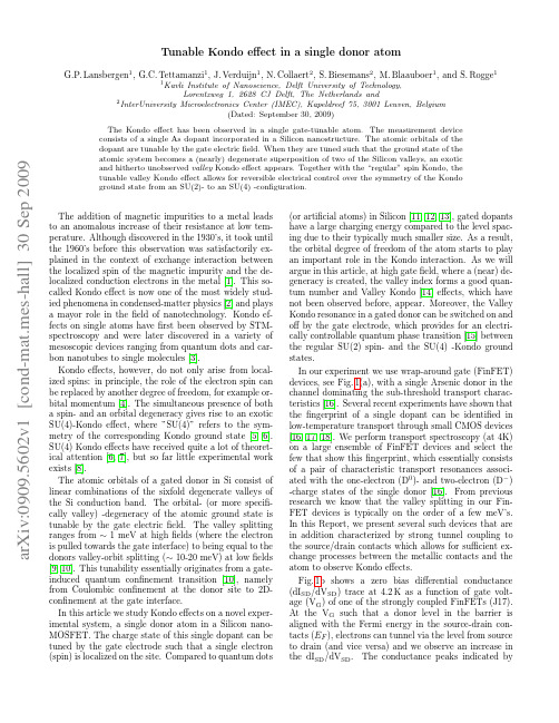
Tunable Kondo effect in a single donor atomnsbergen 1,G.C.Tettamanzi 1,J.Verduijn 1,N.Collaert 2,S.Biesemans 2,M.Blaauboer 1,and S.Rogge 11Kavli Institute of Nanoscience,Delft University of Technology,Lorentzweg 1,2628CJ Delft,The Netherlands and2InterUniversity Microelectronics Center (IMEC),Kapeldreef 75,3001Leuven,Belgium(Dated:September 30,2009)The Kondo effect has been observed in a single gate-tunable atom.The measurement device consists of a single As dopant incorporated in a Silicon nanostructure.The atomic orbitals of the dopant are tunable by the gate electric field.When they are tuned such that the ground state of the atomic system becomes a (nearly)degenerate superposition of two of the Silicon valleys,an exotic and hitherto unobserved valley Kondo effect appears.Together with the “regular”spin Kondo,the tunable valley Kondo effect allows for reversible electrical control over the symmetry of the Kondo ground state from an SU(2)-to an SU(4)-configuration.The addition of magnetic impurities to a metal leads to an anomalous increase of their resistance at low tem-perature.Although discovered in the 1930’s,it took until the 1960’s before this observation was satisfactorily ex-plained in the context of exchange interaction between the localized spin of the magnetic impurity and the de-localized conduction electrons in the metal [1].This so-called Kondo effect is now one of the most widely stud-ied phenomena in condensed-matter physics [2]and plays a mayor role in the field of nanotechnology.Kondo ef-fects on single atoms have first been observed by STM-spectroscopy and were later discovered in a variety of mesoscopic devices ranging from quantum dots and car-bon nanotubes to single molecules [3].Kondo effects,however,do not only arise from local-ized spins:in principle,the role of the electron spin can be replaced by another degree of freedom,for example or-bital momentum [4].The simultaneous presence of both a spin-and an orbital degeneracy gives rise to an exotic SU(4)-Kondo effect,where ”SU(4)”refers to the sym-metry of the corresponding Kondo ground state [5,6].SU(4)Kondo effects have received quite a lot of theoret-ical attention [6,7],but so far little experimental work exists [8].The atomic orbitals of a gated donor in Si consist of linear combinations of the sixfold degenerate valleys of the Si conduction band.The orbital-(or more specifi-cally valley)-degeneracy of the atomic ground state is tunable by the gate electric field.The valley splitting ranges from ∼1meV at high fields (where the electron is pulled towards the gate interface)to being equal to the donors valley-orbit splitting (∼10-20meV)at low fields [9,10].This tunability essentially originates from a gate-induced quantum confinement transition [10],namely from Coulombic confinement at the donor site to 2D-confinement at the gate interface.In this article we study Kondo effects on a novel exper-imental system,a single donor atom in a Silicon nano-MOSFET.The charge state of this single dopant can be tuned by the gate electrode such that a single electron (spin)is localized on the pared to quantum dots (or artificial atoms)in Silicon [11,12,13],gated dopants have a large charging energy compared to the level spac-ing due to their typically much smaller size.As a result,the orbital degree of freedom of the atom starts to play an important role in the Kondo interaction.As we will argue in this article,at high gate field,where a (near)de-generacy is created,the valley index forms a good quan-tum number and Valley Kondo [14]effects,which have not been observed before,appear.Moreover,the Valley Kondo resonance in a gated donor can be switched on and offby the gate electrode,which provides for an electri-cally controllable quantum phase transition [15]between the regular SU(2)spin-and the SU(4)-Kondo ground states.In our experiment we use wrap-around gate (FinFET)devices,see Fig.1(a),with a single Arsenic donor in the channel dominating the sub-threshold transport charac-teristics [16].Several recent experiments have shown that the fingerprint of a single dopant can be identified in low-temperature transport through small CMOS devices [16,17,18].We perform transport spectroscopy (at 4K)on a large ensemble of FinFET devices and select the few that show this fingerprint,which essentially consists of a pair of characteristic transport resonances associ-ated with the one-electron (D 0)-and two-electron (D −)-charge states of the single donor [16].From previous research we know that the valley splitting in our Fin-FET devices is typically on the order of a few meV’s.In this Report,we present several such devices that are in addition characterized by strong tunnel coupling to the source/drain contacts which allows for sufficient ex-change processes between the metallic contacts and the atom to observe Kondo effects.Fig.1b shows a zero bias differential conductance (dI SD /dV SD )trace at 4.2K as a function of gate volt-age (V G )of one of the strongly coupled FinFETs (J17).At the V G such that a donor level in the barrier is aligned with the Fermi energy in the source-drain con-tacts (E F ),electrons can tunnel via the level from source to drain (and vice versa)and we observe an increase in the dI SD /dV SD .The conductance peaks indicated bya r X i v :0909.5602v 1 [c o n d -m a t .m e s -h a l l ] 30 S e p 2009FIG.1:Coulomb blocked transport through a single donor in FinFET devices(a)Colored Scanning Electron Micrograph of a typical FinFET device.(b)Differential conductance (dI SD/dV SD)versus gate voltage at V SD=0.(D0)and(D−) indicate respectively the transport resonances of the one-and two-electron state of a single As donor located in the Fin-FET channel.Inset:Band diagram of the FinFET along the x-axis,with the(D0)charge state on resonance.(c)and(d) Colormap of the differential conductance(dI SD/dV SD)as a function of V SD and V G of samples J17and H64.The red dots indicate the(D0)resonances and data were taken at1.6 K.All the features inside the Coulomb diamonds are due to second-order chargefluctuations(see text).(D0)and(D−)are the transport resonances via the one-electron and two-electron charge states respectively.At high gate voltages(V G>450mV),the conduction band in the channel is pushed below E F and the FET channel starts to open.The D−resonance has a peculiar double peak shape which we attribute to capacitive coupling of the D−state to surrounding As atoms[19].The current between the D0and the D−charge state is suppressed by Coulomb blockade.The dI SD/dV SD around the(D0)and(D−)resonances of sample J17and sample H64are depicted in Fig.1c and Fig.1d respectively.The red dots indicate the po-sitions of the(D0)resonance and the solid black lines crossing the red dots mark the outline of its conducting region.Sample J17shows afirst excited state at inside the conducting region(+/-2mV),indicated by a solid black line,associated with the valley splitting(∆=2 mV)of the ground state[10].The black dashed lines indicate V SD=0.Inside the Coulomb diamond there is one electron localized on the single As donor and all the observable transport in this regionfinds its origin in second-order exchange processes,i.e.transport via a vir-tual state of the As atom.Sample J17exhibits three clear resonances(indicated by the dashed and dashed-dotted black lines)starting from the(D0)conducting region and running through the Coulomb diamond at-2,0and2mV. The-2mV and2mV resonances are due to a second or-der transition where an electron from the source enters one valley state,an the donor-bound electron leaves from another valley state(see Fig.2(b)).The zero bias reso-nance,however,is typically associated with spin Kondo effects,which happen within the same valley state.In sample H64,the pattern of the resonances looks much more complicated.We observe a resonance around0mV and(interrupted)resonances that shift in V SD as a func-tion of V G,indicating a gradual change of the internal level spectrum as a function of V G.We see a large in-crease in conductance where one of the resonances crosses V SD=0(at V G∼445mV,indicated by the red dashed elipsoid).Here the ground state has a full valley degen-eracy,as we will show in thefinal paragraph.There is a similar feature in sample J17at V G∼414mV in Fig.1c (see also the red cross in Fig.1b),although that is prob-ably related to a nearby defect.Because of the relative simplicity of its differential conductance pattern,we will mainly use data obtained from sample J17.In order to investigate the behavior at the degeneracy point of two valley states we use sample H64.In the following paragraphs we investigate the second-order transport in more detail,in particular its temper-ature dependence,fine-structure,magneticfield depen-dence and dependence on∆.We start by analyzing the temperature(T)dependence of sample J17.Fig.2a shows dI SD/dV SD as a function of V SD inside the Coulomb diamond(at V G=395mV) for a range of temperatures.As can be readily observed from Fig.2a,both the zero bias resonance and the two resonances at V SD=+/-∆mV are suppressed with increasing T.The inset of Fig.2a shows the maxima (dI/dV)MAX of the-2mV and0mV resonances as a function of T.We observe a logarithmic dependence on T(a hallmark sign of Kondo correlations)at both resonances,as indicated by the red line.To investigate this point further we analyze another sample(H67)which has sharper resonances and of which more temperature-dependent data were obtained,see Fig.2c.This sample also exhibits the three resonances,now at∼-1,0and +1mV,and the same strong suppression by tempera-ture.A linear background was removed for clarity.We extracted the(dI/dV)MAX of all three resonances forFIG.2:Electrical transport through a single donor atom in the Coulomb blocked region(a)Differential conductance of sample J17as a function of V SD in the Kondo regime(at V G=395mV).For clarity,the temperature traces have been offset by50nS with respect to each other.Both the resonances with-and without valley-stateflip scale similarly with increasing temperature. Inset:Conductance maxima of the resonances at V SD=-2mV and0mV as a function of temperature.(b)Schematic depiction of three(out of several)second-order processes underlying the zero bias and±∆resonances.(c)Differential conductance of sample H67as a function of V SD in the Kondo regime between0.3K and6K.A linear(and temperature independent) background on the order of1µS was removed and the traces have been offset by90nS with respect to each other for clarity.(d)The conductance maxima of the three resonances of(c)normalized to their0.3K value.The red line is afit of the data by Eq.1.all temperatures and normalized them to their respective(dI/dV)MAX at300mK.The result is plotted in Fig.2d.We again observe that all three peaks have the same(log-arithmic)dependence on temperature.This dependenceis described well by the following phenomenological rela-tionship[20](dI SD/dV SD)max (T)=(dI SD/dV SD)T 2KT2+TKs+g0(1)where TK =T K/√21/s−1,(dI SD/dV SD)is the zero-temperature conductance,s is a constant equal to0.22 [21]and g0is a constant.Here T K is the Kondo tem-perature.The red curve in Fig.2d is afit of Eq.(1)to the data.We readily observe that the datafit well and extract a T K of2.7K.The temperature scaling demon-strates that both the no valley-stateflip resonance at zero bias voltage and the valley-stateflip-resonance atfinite bias are due to Kondo-type processes.Although a few examples offinite-bias Kondo have been reported[15,22,23],the corresponding resonances (such as our±∆resonances)are typically associated with in-elastic cotunneling.Afinite bias between the leads breaks the coherence due to dissipative transitions in which electrons are transmitted from the high-potential-lead to the low-potential lead[24].These dissipative4transitions limit the lifetime of the Kondo-type processes and,if strong enough,would only allow for in-elastic events.In the supporting online text we estimate the Kondo lifetime in our system and show it is large enough to sustain thefinite-bias Kondo effects.The Kondo nature of the+/-∆mV resonances points strongly towards a Valley Kondo effect[14],where co-herent(second-order)exchange between the delocalized electrons in the contacts and the localized electron on the dopant forms a many-body singlet state that screens the valley index.Together with the more familiar spin Kondo effect,where a many-body state screens the spin index, this leads to an SU(4)-Kondo effect,where the spin and charge degree of freedom are fully entangled[8].The ob-served scaling of the+/-∆-and zero bias-resonances in our samples by a single T K is an indication that such a fourfold degenerate SU(4)-Kondo ground state has been formed.To investigate the Kondo nature of the transport fur-ther,we analyze the substructure of the resonances of sample J17,see Fig.2a.The central resonance and the V SD=-2mV each consist of three separate peaks.A sim-ilar substructure can be observed in sample H67,albeit less clear(see Fig.2c).The substructure can be explained in the context of SU(4)-Kondo in combination with a small difference between the coupling of the ground state (ΓGS)-and thefirst excited state(ΓE1)-to the leads.It has been theoretically predicted that even a small asym-metry(ϕ≡ΓE1/ΓGS∼=1)splits the Valley Kondo den-sity of states into an SU(2)-and an SU(4)-part[25].Thiswill cause both the valley-stateflip-and the no valley-stateflip resonances to split in three,where the middle peak is the SU(2)-part and the side-peaks are the SU(4)-parts.A more detailed description of the substructure can be found in the supporting online text.The split-ting between middle and side-peaks should be roughly on the order of T K[25].The measured splitting between the SU(2)-and SU(4)-parts equals about0.5meV for sample J17and0.25meV for sample H67,which thus corresponds to T K∼=6K and T K∼=3K respectively,for the latter in line with the Kondo temperature obtained from the temperature dependence.We further note that dI SD/dV SD is smaller than what we would expect for the Kondo conductance at T<T K.However,the only other study of the Kondo effect in Silicon where T K could be determined showed a similar magnitude of the Kondo signal[12].The presence of this substructure in both the valley-stateflip-,and the no valley-stateflip-Kondo resonance thus also points at a Valley Kondo effect.As a third step,we turn our attention to the magnetic field(B)dependence of the resonances.Fig.3shows a colormap plot of dI SD/dV SD for samples J17and H64 both as a function of V SD and B at300mK.The traces were again taken within the Coulomb diamond.Atfinite magneticfield,the central Kondo resonances of both de-vices split in two with a splitting of2.2-2.4mV at B=FIG.3:Colormap plot of the conductance as a function of V SD and B of sample J17at V G=395mV(a)and H64at V G=464mV(b).The central Kondo resonances split in two lines which are separated by2g∗µB B.The resonances with a valley-stateflip do not seem to split in magneticfield,a feature we associate with the different decay-time of parallel and anti-parallel spin-configurations of the doubly-occupied virtual state(see text).10T.From theoretical considerations we expect the cen-tral Valley Kondo resonance to split in two by∆B= 2g∗µB B if there is no mixing of valley index(this typical 2g∗µB B-splitting of the resonances is one of the hall-marks of the Kondo effect[24]),and to split in three (each separated by g∗µB B)if there is a certain degree of valley index mixing[14].Here,g∗is the g-factor(1.998 for As in Si)andµB is the Bohr magneton.In the case of full mixing of valley index,the valley Kondo effect is expected to vanish and only spin Kondo will remain [25].By comparing our measured magneticfield splitting (∆B)with2g∗µB B,wefind a g-factor between2.1and 2.4for all three devices.This is comparable to the result of Klein et al.who found a g-factor for electrons in SiGe quantum dots in the Kondo regime of around2.2-2.3[13]. The magneticfield dependence of the central resonance5indicates that there is no significant mixing of valley in-dex.This is an important observation as the occurrence of Valley Kondo in Si depends on the absence of mix-ing(and thus the valley index being a good quantum number in the process).The conservation of valley in-dex can be attributed to the symmetry of our system. The large2D-confinement provided by the electricfield gives strong reason to believe that the ground-andfirst excited-states,E GS and E1,consist of(linear combi-nations of)the k=(0,0,±kz)valleys(with z in the electricfield direction)[10,26].As momentum perpen-dicular to the tunneling direction(k x,see Fig.1)is con-served,also valley index is conserved in tunneling[27]. The k=(0,0,±k z)-nature of E GS and E1should be as-sociated with the absence of significant exchange interac-tion between the two states which puts them in the non-interacting limit,and thus not in the correlated Heitler-London limit where singlets and triplets are formed.We further observe that the Valley Kondo resonances with a valley-stateflip do not split in magneticfield,see Fig.3.This behavior is seen in both samples,as indicated by the black straight solid lines,and is most easily ob-served in sample J17.These valley-stateflip resonances are associated with different processes based on their evo-lution with magneticfield.The processes which involve both a valleyflip and a spinflip are expected to shift to energies±∆±g∗µB B,while those without a spin-flip stay at energies±∆[14,25].We only seem to observe the resonances at±∆,i.e.the valley-stateflip resonances without spinflip.In Ref[8],the processes with both an orbital and a spinflip also could not be observed.The authors attribute this to the broadening of the orbital-flip resonances.Here,we attribute the absence of the processes with spinflip to the difference in life-time be-tween the virtual valley state where two spins in seperate valleys are parallel(τ↑↑)and the virtual state where two spins in seperate valleys are anti-parallel(τ↑↓).In con-trast to the latter,in the parallel spin configuration the electron occupying the valley state with energy E1,can-not decay to the other valley state at E GS due to Pauli spin blockade.It wouldfirst needs toflip its spin[28].We have estimatedτ↑↑andτ↑↓in our system(see supporting online text)andfind thatτ↑↑>>h/k b T K>τ↑↓,where h/k b T K is the characteristic time-scale of the Kondo pro-cesses.Thus,the antiparallel spin configuration will have relaxed before it has a change to build up a Kondo res-onance.Based on these lifetimes,we do not expect to observe the Kondo resonances associated with both an valley-state-and a spin-flip.Finally,we investigate the degeneracy point of valley states in the Coulomb diamond of sample H64.This degeneracy point is indicated in Fig.1d by the red dashed ellipsoid.By means of the gate electrode,we can tune our system onto-or offthis degeneracy point.The gate-tunability in this sample is created by a reconfiguration of the level spectrum between the D0and D−-charge states,FIG.4:Colormap plot of I SD at V SD=0as a function of V G and B.For increasing B,a conductance peak develops around V G∼450mV at the valley degeneracy point(∆= 0),indicated by the dashed black line.Inset:Magneticfield dependence of the valley degeneracy point.The resonance is fixed at zero bias and its magnitude does not depend on the magneticfield.probably due to Coulomb interactions in the D−-states. Figure4shows a colormap plot of I SD at V SD=0as a function of V G and B(at0.3K).Note that we are thus looking at the current associated with the central Kondo resonance.At B=0,we observe an increasing I SD for higher V G as the atom’s D−-level is pushed toward E F. As B is increased,the central Kondo resonance splits and moves away from V SD=0,see Fig.3.This leads to a general decrease in I SD.However,at around V G= 450mV a peak in I SD develops,indicated by the dashed black line.The applied B-field splits offthe resonances with spin-flip,but it is the valley Kondo resonance here that stays at zero bias voltage giving rise to the local current peak.The inset of Fig.4shows the single Kondo resonance in dI SD/dV SD as a function of V SD and B.We observe that the magnitude of the resonance does not decrease significantly with magneticfield in contrast to the situation at∆=0(Fig.3b).This insensitivity of the Kondo effect to magneticfield which occurs only at∆= 0indicates the profound role of valley Kondo processes in our structure.It is noteworthy to mention that at this specific combination of V SD and V G the device can potentially work as a spin-filter[6].We acknowledge fruitful discussions with Yu.V. Nazarov,R.Joynt and S.Shiau.This project is sup-ported by the Dutch Foundation for Fundamental Re-search on Matter(FOM).6[1]Kondo,J.,Resistance Minimum in Dilute Magnetic Al-loys,Prog.Theor.Phys.3237-49(1964)[2]Hewson,A.C.,The Kondo Problem to Heavy Fermions(Cambridge Univ.Press,Cambridge,1993).[3]Wingreen N.S.,The Kondo effect in novel systems,Mat.Science Eng.B842225(2001)and references therein.[4]Cox,D.L.,Zawadowski,A.,Exotic Kondo effects in met-als:magnetic ions in a crystalline electricfield and tun-neling centers,Adv.Phys.47,599-942(1998)[5]Inoshita,T.,Shimizu, A.,Kuramoto,Y.,Sakaki,H.,Correlated electron transport through a quantum dot: the multiple-level effect.Phys.Rev.B48,14725-14728 (1993)[6]Borda,L.Zar´a nd,G.,Hofstetter,W.,Halperin,B.I.andvon Delft,J.,SU(4)Fermi Liquid State and Spin Filter-ing in a Double Quantum Dot System,Phys.Rev.Lett.90,026602(2003)[7]Zar´a nd,G.,Orbitalfluctuations and strong correlationsin quantum dots,Philosophical Magazine,86,2043-2072 (2006)[8]Jarillo-Herrero,P.,Kong,J.,van der Zant H.S.J.,Dekker,C.,Kouwenhoven,L.P.,De Franceschi,S.,Or-bital Kondo effect in carbon nanotubes,Nature434,484 (2005)[9]Martins,A.S.,Capaz,R.B.and Koiller,B.,Electric-fieldcontrol and adiabatic evolution of shallow donor impuri-ties in silicon,Phys.Rev.B69,085320(2004)[10]Lansbergen,G.P.et al.,Gate induced quantum confine-ment transition of a single dopant atom in a Si FinFET, Nature Physics4,656(2008)[11]Rokhinson,L.P.,Guo,L.J.,Chou,S.Y.,Tsui, D.C.,Kondo-like zero-bias anomaly in electronic transport through an ultrasmall Si quantum dot,Phys.Rev.B60, R16319-R16321(1999)[12]Specht,M.,Sanquer,M.,Deleonibus,S.,Gullegan G.,Signature of Kondo effect in silicon quantum dots,Eur.Phys.J.B26,503-508(2002)[13]Klein,L.J.,Savage, D.E.,Eriksson,M.A.,Coulombblockade and Kondo effect in a few-electron silicon/silicon-germanium quantum dot,Appl.Phys.Lett.90,033103(2007)[14]Shiau,S.,Chutia,S.and Joynt,R.,Valley Kondo effectin silicon quantum dots,Phys.Rev.B75,195345(2007) [15]Roch,N.,Florens,S.,Bouchiat,V.,Wernsdirfer,W.,Balestro, F.,Quantum phase transistion in a single molecule quantum dot,Nature453,633(2008)[16]Sellier,H.et al.,Transport Spectroscopy of a SingleDopant in a Gated Silicon Nanowire,Phys.Rev.Lett.97,206805(2006)[17]Calvet,L.E.,Wheeler,R.G.and Reed,M.A.,Observa-tion of the Linear Stark Effect in a Single Acceptor in Si, Phys.Rev.Lett.98,096805(2007)[18]Hofheinz,M.et al.,Individual charge traps in siliconnanowires,Eur.Phys.J.B54,299307(2006)[19]Pierre,M.,Hofheinz,M.,Jehl,X.,Sanquer,M.,Molas,G.,Vinet,M.,Deleonibus S.,Offset charges acting as ex-cited states in quantum dots spectroscopy,Eur.Phys.J.B70,475-481(2009)[20]Goldhaber-Gordon,D.,Gres,J.,Kastner,M.A.,Shtrik-man,H.,Mahalu, D.,Meirav,U.,From the Kondo Regime to the Mixed-Valence Regime in a Single-Electron Transistor,Phys.Rev.Lett.81,5225(1998) [21]Although the value of s=0.22stems from SU(2)spinKondo processes,it is valid for SU(4)-Kondo systems as well[8,25].[22]Paaske,J.,Rosch,A.,W¨o lfle,P.,Mason,N.,Marcus,C.M.,Nyg˙ard,Non-equilibrium singlet-triplet Kondo ef-fect in carbon nanotubes,Nature Physics2,460(2006) [23]Osorio, E.A.et al.,Electronic Excitations of a SingleMolecule Contacted in a Three-Terminal Configuration, Nanoletters7,3336-3342(2007)[24]Meir,Y.,Wingreen,N.S.,Lee,P.A.,Low-TemperatureTransport Through a Quantum Dot:The Anderson Model Out of Equilibrium,Phys.Rev.Lett.70,2601 (1993)[25]Lim,J.S.,Choi,M-S,Choi,M.Y.,L´o pez,R.,Aguado,R.,Kondo effects in carbon nanotubes:From SU(4)to SU(2)symmetry,Phys.Rev.B74,205119(2006) [26]Hada,Y.,Eto,M.,Electronic states in silicon quan-tum dots:Multivalley artificial atoms,Phys.Rev.B68, 155322(2003)[27]Eto,M.,Hada,Y.,Kondo Effect in Silicon QuantumDots with Valley Degeneracy,AIP Conf.Proc.850,1382-1383(2006)[28]A comparable process in the direct transport throughSi/SiGe double dots(Lifetime Enhanced Transport)has been recently proposed[29].[29]Shaji,N.et.al.,Spin blockade and lifetime-enhancedtransport in a few-electron Si/SiGe double quantum dot, Nature Physics4,540(2008)7Supporting InformationFinFET DevicesThe FinFETs used in this study consist of a silicon nanowire connected to large contacts etched in a60nm layer of p-type Silicon On Insulator.The wire is covered with a nitrided oxide(1.4nm equivalent SiO2thickness) and a narrow poly-crystalline silicon wire is deposited perpendicularly on top to form a gate on three faces.Ion implantation over the entire surface forms n-type degen-erate source,drain,and gate electrodes while the channel protected by the gate remains p-type,see Fig.1a of the main article.The conventional operation of this n-p-n field effect transistor is to apply a positive gate voltage to create an inversion in the channel and allow a current toflow.Unintentionally,there are As donors present be-low the Si/SiO2interface that show up in the transport characteristics[1].Relation between∆and T KThe information obtained on T K in the main article allows us to investigate the relation between the splitting (∆)of the ground(E GS)-andfirst excited(E1)-state and T K.It is expected that T K decreases as∆increases, since a high∆freezes out valley-statefluctuations.The relationship between T K of an SU(4)system and∆was calculated by Eto[2]in a poor mans scaling approach ask B T K(∆) B K =k B T K(∆=0)ϕ(2)whereϕ=ΓE1/ΓGS,withΓE1andΓGS the lifetimes of E1and E GS respectively.Due to the small∆com-pared to the barrier height between the atom and the source/drain contact,we expectϕ∼1.Together with ∆=1meV and T K∼2.7K(for sample H67)and∆=2meV and T K∼6K(for sample J17),Eq.2yields k B T K(∆)/k B T K(∆=0)=0.4and k B T K(∆)/k B T K(∆= 0)=0.3respectively.We can thus conclude that the rela-tively high∆,which separates E GS and E1well in energy, will certainly quench valley-statefluctuations to a certain degree but is not expected to reduce T K to a level that Valley effects become obscured.Valley Kondo density of statesHere,we explain in some more detail the relation be-tween the density of states induced by the Kondo effects and the resulting current.The Kondo density of states (DOS)has three main peaks,see Fig.1a.A central peak at E F=0due to processes without valley-stateflip and two peaks at E F=±∆due to processes with valley-state flip,as explained in the main text.Even a small asym-metry(ϕclose to1)will split the Valley Kondo DOS into an SU(2)-and an SU(4)-part[3],indicated in Fig1b in black and red respectively.The SU(2)-part is positioned at E F=0or E F=±∆,while the SU(4)-part will be shifted to slightly higher positive energy(on the order of T K).A voltage bias applied between the source and FIG.1:(a)dI SD/dV SD as a function of V SD in the Kondo regime(at395mV G)of sample J17.The substructure in the Kondo resonances is the result of a small difference between ΓE1andΓGS.This splits the peaks into a(central)SU(2)-part (black arrows)and two SU(4)-peaks(red arrows).(b)Density of states in the channel as a result ofϕ(=ΓE1/ΓGS)<1and applied V SD.drain leads results in the Kondo peaks to split,leaving a copy of the original structure in the DOS now at the E F of each lead,which is schematically indicated in Fig.1b by a separate DOS associated with each contact.The current density depends directly on the density of states present within the bias window defined by source/drain (indicated by the gray area in Fig1b)[4].The splitting between SU(2)-and SU(4)-processes will thus lead to a three-peak structure as a function of V SD.Figure.1a has a few more noteworthy features.The zero-bias resonance is not positioned exactly at V SD=0, as can also be observed in the transport data(Fig1c of the main article)where it is a few hundredµeV above the Fermi energy near the D0charge state and a few hundredµeV below the Fermi energy near the D−charge state.This feature is also known to arise in the Kondo strong coupling limit[5,6].We further observe that the resonances at V SD=+/-2mV differ substantially in magnitude.This asymmetry between the two side-peaks can actually be expected from SU(4)Kondo sys-tems where∆is of the same order as(but of course al-ways smaller than)the energy spacing between E GS and。
量子物理的秘密英语作文
量子物理的秘密英语作文The Secrets of Quantum Physics。
Quantum physics is a branch of science that deals with the behavior of particles at the atomic and subatomic levels. It is a field that has fascinated scientists and researchers for decades, and continues to be the subject of much study and debate. The secrets of quantum physics are both mysterious and intriguing, and have the potential to revolutionize our understanding of the universe.One of the most fascinating aspects of quantum physics is the concept of duality, which refers to the idea that particles can exhibit both wave-like and particle-like behavior. This duality is best exemplified by the famous double-slit experiment, in which particles such as electrons are fired at a barrier with two slits. When the particles pass through the slits, they create an interference pattern on the other side, as if they were waves. However, when a detector is placed to observe whichslit the particles pass through, the interference pattern disappears and the particles behave as individual particles. This phenomenon has baffled scientists for years, and continues to be a subject of much debate and speculation.Another intriguing aspect of quantum physics is the concept of entanglement, which refers to the phenomenon in which two particles become connected in such a way that the state of one particle is instantly correlated with thestate of the other, regardless of the distance between them. This phenomenon was famously described by Albert Einsteinas "spooky action at a distance," and has been the subjectof much study and experimentation. The implications of entanglement are profound, and have the potential to revolutionize the field of communication and information technology.Furthermore, quantum physics has also led to the development of new and exciting technologies, such as quantum computing and quantum cryptography. Quantum computing utilizes the principles of quantum mechanics to perform complex calculations at speeds that are far beyondthe capabilities of traditional computers. This has the potential to revolutionize fields such as cryptography,drug discovery, and materials science. Quantum cryptography, on the other hand, utilizes the principles of quantum mechanics to create secure communication channels that are immune to eavesdropping and hacking. This has the potential to revolutionize the field of cybersecurity and information technology.In conclusion, the secrets of quantum physics are both mysterious and intriguing, and have the potential to revolutionize our understanding of the universe. The concepts of duality, entanglement, and quantum technologies have the potential to transform the way we think about the world around us, and have the potential to revolutionize fields such as communication, computing, and cybersecurity. As our understanding of quantum physics continues to evolve, it is likely that we will continue to unlock the secrets of the universe and develop new and exciting technologies that will shape the future of humanity.。
- 1、下载文档前请自行甄别文档内容的完整性,平台不提供额外的编辑、内容补充、找答案等附加服务。
- 2、"仅部分预览"的文档,不可在线预览部分如存在完整性等问题,可反馈申请退款(可完整预览的文档不适用该条件!)。
- 3、如文档侵犯您的权益,请联系客服反馈,我们会尽快为您处理(人工客服工作时间:9:00-18:30)。
a r X i v :c o n d -m a t /0703380v 1 [c o n d -m a t .m e s -h a l l ] 14 M a r 2007Conductance of a quantum point contact based on spin-density-functional theoryS.Ihnatsenka and I.V.ZozoulenkoSolid State Electronics,Department of Science and Technology (ITN),Link¨o ping University,60174Norrk¨o ping,Sweden(Dated:February 6,2008)We present full quantum mechanical conductance calculations of a quantum point contact (QPC)performed in the framework of the density functional theory (DFT)in the local spin-density ap-proximation (LDA).We start from a lithographical layout of the device and the whole structure,including semi-infinitive leads,is treated on the same footing (i.e.the electron-electron interac-tion is accounted for in both the leads as well as in the central device region).We show that a spin-degeneracy of the conductance channels is lifted and the total conductance exhibits a broad plateau-like feature at ∼0.5×2e 2/h .The lifting of the spin-degeneracy is a generic feature of all studied QPC structures (both very short and very long ones;with the lengths in the range 40 l 500nm).The calculated conductance also shows a hysteresis for forward-and backward sweeps of the gate voltage.These features in the conductance can be traced to the formation of weakly coupled quasi-bound states (magnetic impurities)inside the QPC (also predicted in previous DFT-based studies).A comparison of obtained results with the experimental data shows however,that while the spin-DFT based ”first-principle”calculations exhibits the spin polarization in the QPC,the calculated conductance clearly does not reproduce the 0.7anomaly observed in almost all QPCs of various geometries.We critically examine major features of the standard DFT-based ap-proach to the conductance calculations and argue that its inability to reproduce the 0.7anomaly might be related to the infamous derivative discontinuity problem of the DFT leading to spurious self-interaction errors not corrected in the standard LDA.Our results indicate that the formation of the magnetic impurities in the QPC might be an artefact of the LDA when localization of charge is expected to occur.We thus argue that an accurate description of the QPC structure would require approaches that go beyond the standard DFT+LDA schemes.I.INTRODUCTIONExperimental evidence of an additional 0.7×2e 2/h conductance feature in quantum point contacts (QPCs)1,2,3,4,5,6,7,8,9,10has generated enormous theoret-ical activity during recent decade 6,7,8,11,12,13,14,15,16,17,18.While a usual conductance quantization in terms of 2e 2/h can be successfully explained in a one-electron picture 19,no consensus on the origin of the 0.7anomaly has been reached so far.Experimental data,based on magnetic field dependence of the plateau position 1,2and observation of the zero bias anomaly 6clearly point out at spin origin of this effect.The spin origin was adopted in many theories which include,just to name a few of them,a spontaneous spin-polarization inside the constriction of the QPC origi-nated from the exchange-correlation interaction 11,12,13,14,the ferromagnetic-antiferromagnetic exchange interac-tion with a large localized spin 18,a formation of polar-ized quasi-bound states and Kondo effect 15,16,as well as several others.However,none of the existing theories re-produce quantitatively the 0.7conductance anomaly ob-served in almost all QPCs 1,2,3,4,5,6,7,8.Note that some of approaches based on phenomenological models do re-cover the 0.7feature in the conductance 7,8,20.Such the approaches,while providing an important insight for an interpretation of the experiment,are not,however,able to uncover the microscopic origin on the observed effect.A powerful technique capable of providing detailed in-formation about electronic and transport properties on the microscopic level is based on the ”first principle”den-sity functional theory (DFT)approach.The spin DFT calculations addressing the 0.7anomaly in the QPC have been presented by various groups 11,12,13,14,15,17.How-ever,many of these calculations show rather conflicting results.For example.Refs.15,16,17attribute the 0.7anomaly to formation of the localized magnetic moment in the QPC,whereas such quasi-bound states are not re-covered in Refs.11,12,13,14.In contrast,Ref.12relates the 0.7anomaly to multiple metastable spin-polarized solutions.The recent study of Jaksch et al.13suggests that the spin polarization is absent in short QPCs and is increased with the increase of the length of the QCP.This seems to contradict the results reported by Rejec and Meir 17who find that a strong spin polarization due to the magnetic impurity formation is a generic feature seen in short as well as in long QPCs.Motivated by the above mentioned conflicting results and conclusions,in this paper we perform “first princi-ple”full quantum mechanical transport calculations of the conductance of the QPC based on the spin DFT in the local spin-density approximation (LDA).[We use a notation “first principle”in a sense that we start from a lithographical geometry of the gates and a heterostruc-ture layout].The main features of our calculations and the relation of our model to the DFT-based calculations reported previously are as follow.In the present paper the QPC is viewed as an inherently open system where the solution of the Schr¨o dinger equation consists of con-tinuous scattering states.This is in contrast to Refs.11,13treating a QPC as a closed system where the so-lution of the Schrodinger equation is represented by a2discrete set of the eigenfunctions.In our calculations we start from a lithographical layout of the device,which is in contrast to Ref.14using a simplified model of an external confinement potential.(Note that importance of an accurate treatment of the confinement potential is stressed in Ref.8,where the phenomenology and ex-perimental data indicate that the0.7feature depends strongly on the potential profile of the contact region). Our model(but not the computational technique)is con-ceptually similar to the one used by Rejec and Meir17(see also Ref.15reporting similarfindings)where a QPC is treated as an open structure and where a realistic model for the external confinement potential due to metallic gates is utilized.In their study Rejec and Meir focus on the calculation of the electron density,predicting the for-mation of a localized spin-degenerate quasi-bound state (magnetic impurity).They did not,however,perform transport conductance calculations so the central ques-tion whether the0.7-anomaly is indeed related to the for-mation of a magnetic impurity has remained unanswered. In the present paper we hence focus on the calculation of the spin-resolved conductance of the quantum point contact.The details of our model and the Hamiltonian are given in Sec.II.In Sec.III we present our method for the cal-culation of the electron density and conductance which is based on the self-consistent Greens function technique combined with the spin DFT in the local spin density approximation.This method is a generalization of a method of Ref.27for the case of spin.The results are presented in Sec.IV.Our calculations reconfirm thefind-ing reported by Rejec and Meir17concerning the forma-tion of the localized spin-degenerate quasi-bound states (magnetic impurities)within the DFT+LDA approach. However,the calculated conductance clearly does not re-produce the0.7anomaly observed in almost all QPCs of various geometries.Instead,the total conductance shows a broad feature peaked at0.5×2e2/h.A similar feature is also present in the range of the gate voltages where a second step in the conductance develops.The calcu-lated conductance also shows a hysteresis for forward-and backward sweeps of the magneticfields.(We stress that all these results are generic;we studied QPS with lengths in the range40-500nm and electron densities in the leads in the range1015m−2−4·1015m−2,with very similar results).In Sec.V we discuss the obtained results and critically examine the DFT+LDA-based con-ductance calculations.We suggest that the failure of the DFT+LDA approach to reproduce quantitatively the0.7 anomaly may be due to the lack of the derivative dis-continuity in the standard LDA approximation(leading to uncorrected self-interaction errors)for the case when localization of charge is expected to occur,so that the magnetic impurity formation may be an artefact of the DFT+LDA approach due to the spuriousself-interaction.FIG.1:(color online)(a)Structure of a quantum point con-tact typically fabricated by a split-gate technique.An inter-nal computational region is attached to two semi-infinite leads which serve as electron reservoirs.The gates of the quantum point contact form a constriction of the length l and the width w;w lead is the distance between the gates defining the leads.(b)A representative calculated electron density.II.MODELWe consider a quantum point contact(QPC)placed between two semi-infinite electron reservoirs.A schematic layout of the device is illustrated in Fig. 1(a).Charge carriers originating from a fully ion-ized donor layer form the two-dimensional electron gas (2DEG)which is buried inside a substrate at the GaAs/Al x Ga1−x As heterointerface at the distance b from the surface.Metallic gates are situated on the top of the heterostructure and define the quantum point contact as well as electron reservoirs that are are represented by uniform quantum wires of the infinite length.The Hamiltonian of the whole system(QPC+leads) within the Kohn-Sham formalism can be written in the form H= σHσ,Hσ=−2322;the Schottky barrier ischosento be V Schottky =0.8eV.The Hartree potential is written in a standard formV H (r )=e 2|r −r ′|−1|r −r ′|2+4b 2,(2)where n (r )= σn σ(r )is the total electron density andthe second term describes the mirror charges placed atthe distance b from the surface,εr =12.9is the dielectricconstant of GaAs,and the integration is performed overthe whole device area including the semi-infinite leads.The exchange-correlation potential V σxc (r )in the lo-cal spin density approximation is given by the functionalderivative 23V σxc =d hdE T σ(E )∂f (E −E F )πℑdE G σ(r ,r ,E )f (E −E F ).(6)Note that G σ(r ,r ,E )is a rapidly varying function of en-ergy.As a result,a direct integration along the real axisin Eq.(6)is rather ineffective as its numerical accu-racy is not sufficient to achieve a convergence of the self-consistent electron density.Because of this,we transformthe integration contour into the complex plane ℑ[E ]>0,where the Green’s function is much more smoother (see Ref.27for details).In order to calculate the Green’s function of the wholesystem (QPC +leads)we divide it into three parts,theinternal region and two semi-infinite leads,as shown inFig.1(a).The internal region consists of the QPC as wellas a part of the leads.In order to link the internal regionand the leads together the self-consistent charge density (and the potential)at both sides must be the same.To fulfill this requirement,we place the semi-infinite leadsfar away from the central region so that the gates defining the QPC do not affect the electron density distribution in the leads.(The distribution is determined solely bythe lead gate voltage,see Fig. 1.)As a result,it is fully justified to approximate the semi-infinitive leads by a uniform quantum wire.The self-consistent solution for the latter can be found by the technique developed in Ref.28.Eventually,the Green’s function of the whole system is calculated by linking the surface Green’s function for the semi-infinite leads (calculated using the technique of Ref.28)and the Green’s function of the internal region with the help of the the Dyson equation 29.All the calculations described above are performed self-consistently in an iterative way until a converged solution for the electron density and potential (and hence for the total Green’s function)is obtained.Having calculated the total self-consistent Green’s function,the scatteringproblem is solved where the scattering states in the leads (both propagating and evanescent)are obtained using the Green’s function technique of Ref.28.Having calculated the Green’s function we can find the local density of states (LDOS)in the QPC 26LDOS σ(x,E )=−1n out i+n in i<10−7,(9)where n =n (r )d r is the total electron number in the internal region during the i -th iteration step.4 In order to trigger a spin-polarized solution we apply atearly iterations a small parallel magneticfield,B=0.05T.Thefinal solution is driven mostly by the exchangeinteraction which is about four orders of magnitude largerthat the Zeeman energy at B=0.05T.The self-consistent calculation are performed for dif-ferent gate voltages.To facilitate the calculations we usea solution from the previous value of the gate voltage asan initial guess for the subsequent one.It is worth not-ing that the modified Broyden’s second method30,whichcan greatly reduce the number of iterations for the case of spinless electrons27,does not lead to reliable convergent results for the case of the spin degree of freedom.IV.RESULTSWe calculate the conductance of a split-gate QPC with following parameters representative for a typical experi-mental structure.The2DEG is buried at b=70nm be-low the surface(the widths of the cap,donor and spacer layers are24nm,36nm and10nm respectively),the donor concentration is0.6·1024m−3.The width of the semi-infinitive leads is w lead=400nm,andthe width of the QPC constriction is w=100nm,see Fig.1(a).The width w is kept constant throughout the paper,while the length is varied in the range l=40−500nm.The gate voltage applied to the gates defining the leads is V lead=−0.73V.With these parameters of the device there are18spin-up and18spin-down channels available for propagation in the leads and the electron density inthe center of the leads is n↑lead =n↓lead=2.2·1015m−2.Such a large number of the channels in the leads makes its DOS to mimic a smooth DOS of the two-dimensional electron gas.The temperature isfixed at T=0.2K for all results presented below.Figure2shows the conductance of QPCs of differ-ent constriction lengths l ranging from l=50nm(a very short QPC)to l=500nm(a long quantum wire-type QPC).The conductance of all QPCs shows a broad plateau-like feature at0.5×2e2/h.As the length of the constriction increases,a dip following0.5-plateau startsto develop in the QPC conductance.An inspection of the spin-resolved conductance demonstrates that0.5fea-ture corresponds to the transmission of only one spin channel(say,spin-up),whereas the second(spin-down) conductance channel is totally suppressed.For long con-strictions(l 300nm)the0.5plateau starts to“wear down”transforming into a broad feature whose maximal amplitude is less than0.5×2e2/h.If the constriction is sufficiently long(l 100nm),a conductance plateau at∼1.5×2e2/h starts to develop and a conductance dip following the1.5-plateau also starts to emerge as the length of the constriction increases.To shed light on a microscopic origin of the0.5×2e2/h conductance feature and the suppression of the spin-down channel let us inspect the charge density and energy structure of the QPC.Figure3shows the charge densities FIG.2:(color online)Conductance of the quantum point contact of different lengths50<l<500nm as a function of the gate voltage V g.The geometrical width of the constriction is w=100nm;the geometrical length l is indicated in the figures.The dashed line corresponds to the spin-unpolarized solution.and the LDOS in the QPC of the length of l=200nm for the case of one transmitted spin-up,G↑=e2/h,and totally blocked spin-down,G↓=0,channel.Near the constriction entrance,the spin-polarized charge droplets (marked by dotted circles in Fig.3(a))are clearly visible. The spin polarization is caused by the exchange interac-tion which dominates the kinetic energy for low densi-ties.The integration of the electron density gives aboutFIG.3:(color online)Formation of quasi-bound states in the quantum point contact.(a)The charge density and(b) the local density of states are shown for the regime of one transmitted spin-up and totally blocked spin-down channel. The left and right columns correspond to spin-up and spin down electrons.The white dashed lines in(b)indicate the self-consistent Kohn-Sham potential along the cross section y=0,Vσ(x,y=0).The charge droplets with approximately one electron trapped are denoted by dotted lines in(a).The geometrical length and width of the QPC are l=200nm and w=100nm,respectively;V g=−0.98V.one particle in each droplet.The quasi-bound states for correspondingdroplets can also be traced in the LDOS shown in Fig.3(b).An inspection of the correspond-ing potential profile for the spin-up electrons reveals that the low-and high energy droplets correspond to respec-tivelyfirst and second quasibound states trapped in the double-barrier potential.At the same time the spin-down droplets are spatially separated by a distance∼100nm. This spatial separation is also reflected in the shape of the total confining potential for the spin-down electrons that forms a wide tunnelling barrier,see Fig.3(b).Because of this barrier,the transmission probability for the spin-down conductance is negligibly small(G↓≈10−5×e2/h). The quasi-bound states are not spatiallyfixed but gradually move during the sweep of the gate voltage,V g. Already in the pinch-offregime,two quasi-bound states are developed at both sides of the constriction.When V g becomes less negative they move towards each other and eventually merge.Because of the exchange inter-action,this occursfirst for the spin-up state and then for the spin-down.As a result,the total conductance G shows quantization in units of e2/h,see Fig.2.We stress that all the results reported above are generic;we studied QPCs with lengths in the range40-500nm and electron densities in the leads in the range1015m−2−4·1015m−2, with very similar results.We also stress that our calcu-lations with two parameterizations of Refs.24,25for the FIG.4:(color online)Convergence of self-consistent calcu-lations for(a)a short QPC(l=100nm)and(b)a long QPC(l=300nm)(y-axis corresponds to the relative density update defined by Eq.(9)).Solid and dashed lines denote spin-up and spin-down solutions,respectively.Insets show the charge densities at the constriction at different stages of iteration procedure.Note,that we used the convergence crite-ria for the relative density update<10−7for all calculations presented in this paper.The geometrical width of the con-striction w=100nm;V g=−1.4V.correlation potential give almost the same results.This is not surprising,because for the system at hand the cor-relation potential is an order of magnitude lower than the exchange potential.Our conclusions concerning formation of the localized quasi-bound states in the QPC agree well with earlier findings of Hirose et al.15and Rejec and Meir17,but do not support the conclusion of Jaksch et al.13that the spin polarization is absent in short QPCs and is increased with the increase of the length of the QCP.We now want to focus on an aspects of the calcula-tions concerning a choice of the criteria for termination of the iteration procedure,Eq.(9).Even though this aspect has a rather technical character,we feel that it is important to address it in detail,as the proper choice of the termination criteria is essential for reaching of theFIG.5:(color online)Conductance hysteresis in the quan-tum point contact for forward-and backward sweeps of the gate voltage(solid and dashed lines respectively).The dot-ted line corresponds to the unpolarized solution exhibiting no hysteresis behavior.Insets show the charge densities in the constriction at V g=−0.975V.The parameters of QPC are l=200nm and w=100nm.spin polarized solution.Figure4shows a relative den-sity update as a function of the number of iterations for a relatively short(l=100nm)and a relatively long (l=300nm)constrictions.For the long constriction the spin polarized solution is obtained already during initial iteration steps and its character does not change with increase of the number of iterations,see Fig.4(b).On the contrary,for a short constriction,the spin polarized solution is obtained only during later stages of iterations, as no spin-polarized solution is present during the initial steps even when the relative density update decreases to ∼10−4,see4(a).Note,that the spin-polarized solu-tion is energetically favorable and more stable than the spin-unpolarized one for all QPC studied.The spin-DFT calculations reported above show the presence of the spin-resolved quasi-bound states confined in an effective double-barrier potential.It is well known that the quasi-bound states often lead to the hysteretic behavior of the system.For example,the hysteresis is commonly observed in the I-V characteristics of the res-onant double-barrier tunnelling structures for forward-and backward voltage sweeps31,32.Such hysteretic be-havior is related to the presence of the quasi-bound state between the barriers and was reproduced in nu-merous calculations32,including those based on the DFT approach33.Our calculations demonstrate that similar hysteretic behavior is present in the conductance of the QPC.When the gate voltage is swept forward and back-wards,the conductance shows the prominent hysteresis in the transition regions between the plateaus,see Fig.5.In the region of hysteresis,the system,depending on the history,can be in one of two different ground states as illustrated in the inset to Fig.5.Because the hystere-sis is present only in the transition regions and is com-pletely absent in the spin-unpolarized solution,its origin is due to the exchange interaction.We would like to stress that existence of two distinct ground states as well as the hysteresis behavior of the system at hand does not contradict to the DFT approach as such.Owing to the nonlinearity of the problem,there might be more than one solution within the DFT framework34.Besides the double-barrier resonant tunnelling structures mentioned above33,the DFT approach was used for the description of the hysteretic behavior of quantum Hall states in the double-layered quantum well structures35,as well as hys-teresis and spin phase transitions in quantum wires in the integer quantum Hall regime36.We however,con-clude this section by noticing that we are not aware of any experimental reports on the observation of the hys-teresis phenomena in the QPC structures.V.DISCUSSIONWe start our discussion from a comparison of the spin DFT-based conductance calculations reported in the pre-ceding section with the experimental conductance of the QPC structures.The calculations show a pronounced plateau-like feature at∼0.5×2e2/h for all QPC struc-tures studied(both short and long ones).For longer QPCs(l 150nm),a dip following0.5-plateau starts to develop in the conductance.At the same time,a new conductance plateau at∼1.5×2e2/h starts to de-velop and a conductance dip following1.5-plateau also starts to emerge as the length of the constriction in-creases(see Fig.2).Our calculations also show a pro-nounced hysteretic behavior in the transition regions be-tween the plateaus for forward and backward sweeps of the gate voltage,Fig. 5.On the contrary,the exper-imental data clearly show an anomaly in the conduc-tance around0.7×2e2/h.[It should be stressed that the calculated0.5plateau corresponds to the complete sup-pression of one spin channel,whereas experimentally ob-served0.7anomaly means that both spin channels have to be present in the conductance].Some experiments8 also indicate a feature around1.7×2e2/h.As far as the hysteresis behavior is concerned,we are not aware of any experimental reports of this effect.The above comparison demonstrates that while the spin-DFT based “first-principle”calculations predict the spin polarization in the QPC structure,the calculated conductance clearly does not reproduce the0.7anomaly observed in almost all QPCs of various geometries.In order to understand why the calculated conduc-tance fails to reproduce the0.7anomaly,let us critically analyze the major features of the DFT-based conduc-tance calculations.Our computation scheme relies on an approach that during recent years became a stan-dard tool for transport calculations in open electronic systems such as molecules,metallic wires and meso-7scopic conductors37,38,39,40,41,42.Its starting point is the Landauer-type formula where the conductance is calcu-lated using the Green’s function or similar scattering techniques combined with the mean-field description of the electronic structure in the leads and in the device re-gion typically based on the ground state self-consistent Kohn-Sham orbitals.Because of the conceptual appeal of this approach,the earlier works were not focused on its formal justification.Recently,however,several studies have provided the rigorous theoretical foundation for the above DFT-based methodologies calculating the steady currents in open electronic systems34,43,44,45.Therefore, the question concerning the validity of the present ap-proach relies mostly on the proper description of the ex-change and correlation within the DFT approximation. We focus below only on two aspects of the DFT approach that seem to be the most important for understanding of the discrepancy between the calculations and the exper-iment.The exchange and correlations are commonly accounted for within the local spin density appromaximation23.As mentioned in preceding sections,for two dimensional systems there are two commonly used parameterizations,namely the param-eterization of Tanatar and Ceperley24and Attacalite et al25.The validity of these approximations was tested for few-electron quantum dot systems and, generally,a very good agreement agreement with the exact diagonalization and/or variational Monte Carlo calculations is found46.Taking into account that these parametrizations give practically the same results for the QPC conductance,we do not expect the utilization of the above parametrizations to be a source of a significant discrepancy between the calculated conductance and the experiment.Instead,we focus on another aspect of the choice of the exchange energy functional which arises in the systems with a variable particle number.(Note that the QPC structure,being an essentially open structure, belongs to this class of systems).This aspect is related to the infamous“derivative discontinuity problem”of the DFT originating from the discontinuous dependence of V xc on the particle number23.(Note that the LDA does not include any derivative discontinuity in the V xc). The problem with the derivative discontinuity(lead-ing to uncompensated self-interaction corrections in the V xc)has been recently recognized in the standard quan-tum mechanical transport calculations in molecular sys-tems and atomic wires43,47,48.Typically,such the calcu-lations provide a good quantitative agreement with the experimental data for systems where the coupling to the leads is strong and the conductance exceeds the conduc-tance unit G0=2e2/h(for example,for atomistic metal-lic wires and related systems).At the same time,for weakly coupled systems such as organic molecules the standard DFT+LDA approach leads to the orders-of-magnitude discrepancy between the measured and cal-culated currents and to incorrect predictions of the con-ducting(instead of experimentally observed insulated)phase43,47,48,49,50.There have been attempts to explain these discrepancies by insufficient modelling,such as atomistic structures or contact coupling.Several recent studies however,attributed this discrepancy to more fun-damental reasons,identifying the lack of the derivative discontinuity in LDA as a major source of error in the DFT-based transport calculations47,48.For example,To-her et al.47argue that LDA approximation is not suit-able for transport calculations for the case of weak cou-pling.They propose a simple corrective scheme based on the removal of the atomic self-interaction.Their correc-tive scheme restores an agrement with the experiment, opening a conduction gap of the I-V characteristics of a molecular junction instead of a metallic behavior follow-ing from the standard DFT+LDA approach.(It is in-teresting to note that similar self-interaction corrections practically do not effect the conductance and electronic density for the case of strongly-coupled systems47).Al-ternative corrective schemes replacing the Kohn-Sham data for the weakly coupled region with their counter-parts obtained from a Hartree-Fock analysis(taking care of the self-interaction problem)are suggested by Evers et al.43and Palacios49.Note that various approaches to the description of quantum transport for the case of weakly coupled systems(accounting for the charge quantization and thus eliminating the self-interaction errors)were dis-cussed in Refs.50,51,52.We argue here that a similar problem related to the derivative discontinuity may be the reason why the stan-dard DFT+LDA approach fail to describe the observed 0.7-anomaly in the QPC.Indeed,the formation of a spin-polarized charge droplet predicted within the DFT+LDA approach implies that electrons are trapped in weakly coupled quasi-bound states in the center of the QPC.As mentioned above,in the case of weak coupling the lack of the derivative discontinuity in the LDA approximation causes the orders-of-magnitude discrepancies between the theory and experiment for the molecular systems.Thus, it would be reasonable to expect that due to the same reason the LDA approximation is not suitable for the case of the QPC structure as well.Because the correc-tive schemes accounting for the derivative discontinuity are shown to strongly affect the electron density and the energy levels in the system,and because of the apparent failure of the standard DFT+LDA approach to repro-duce the0.7anomaly,we conclude that the formation of the magnetic impurities in the QPC might be an artefact of the LDA due to the lack of the derivative discontinuity related to the spurious self-interaction.Based on the above discussion we conclude that an ac-curate description of the QPC structure might require approaches that go beyond the standard DFT+LDA scheme and account for the derivative discontinuity in the V xc or utilize similar corrective schemes eliminat-ing the self-interaction errors of the DFT+LDA.It is not clear at the moment whether the recipes for the ac-counting of the derivative discontinuity and eliminating the self-interaction correction developed for the molecu-。