MAX6358MSUT中文资料
MAX038资料中文

高频信号发生器_______________概述MAX038是一种只需极少外围电路就能实现高 频、高精度输出三角波、锯齿波、正弦波、方波 和脉冲波的精密高频函数发生器芯片。
内部提供 的2.5V 基准电压和一个外接电阻和电容可以控制 输出频率范围在0.1Hz 到20MHz 。
占空比可在较大 的范围内由一个±2.3V的线性信号控制变化,便 于进行脉冲宽度调制和产生锯齿波。
频率调整和 频率扫描可以用同样的方式实现。
占空比和频率 控制是独立的。
通过设置2个TTL 逻辑地址引脚合适的逻辑电 平,能设定正弦波,方波或三角波的输出。
所有 波形的输出都是峰-峰值为±2VP -P 的信号。
低阻 抗输出能力可以达到±20mA。
____________________________性能o 频率调节范围:0.1Hz 到20MHzo 三角波, 锯齿波, 正弦波, 方波和脉冲波 o 频率和占空比独立可调 o 频率扫描范围:350:1 o 可控占空比:15%到85% o 低阻抗输出缓冲器: 0.1Ω o 低失真正弦波: 0.75% o 低温度漂移: 200ppm/°C______________型号信息TTL 逻辑地址引脚SYNC 从内部振荡器输出占 空比固定为50%的信号,不受其它波占空比的影 响,从而同步系统中其它振荡器。
内部振荡器 允许被连接着相位检波器输入端(PDI )的外部 TTL 时钟同步。
型号 MAX038CPP MAX038CWP MAX038C/D MAX038EPP MAX038EWP工作温度 0°C 到 +70°C 0°C 到 +70°C 0°C 到 +70°C -40°C 到 +85°C -40°C 到 +85°C引脚--封装 20 Plastic DIP 20 SO Dice* 20 Plastic DIP 20 SO.__________________应用精密函数信号发生器 压控振荡器 频率调制器*Contact factory for dice specifications.__________________引脚图脉宽调制器 锁相环 频率合成器FSK 发生器(正弦波和方波)________________________________________________________________ Maxim Integrated Products1For free samples & the latest literature: , or phone 1-800-998-8800. For small orders, phone 408-737-7600 ext. 3468MAX038高频信号发生器图1. 内部结构及基本工作电路_______________ 详细说明MAX038是一种高频函数信号发生器,它可以使 用最少的外部元件而产生低失真正弦波,三角波, 锯齿波,方波(脉冲波)。
MAX485中文数据手册资料
MAX485中文资料2009-11-28 14:49MAX485中文资料,MAX485 PDF,DATASHEET,电路图,通讯程序内容介绍:MAX481、MAX483、MAX485、MAX487-MAX491以及MAX1487是用于RS-485与RS-422通信的低功耗收发器,每个器件中都具有一个驱动器和一个接收器。
MAX483、MAX487、MAX488以及MAX489具有限摆率驱动器,可以减小EMI,并降低由不恰当的终端匹配电缆引起的反射,实现最高250kbps 的无差错数据传输。
MAX481、MAX485、MAX490、MAX491、MAX1487的驱动器摆率不受限制,可以实现最高2.5Mbps的传输速率。
这些收发器在驱动器禁用的空载或满载状态下,吸取的电源电流在120(A 至500(A 之间。
另外,MAX481、MAX483与MAX487具有低电流关断模式,仅消耗0.1µA。
所有器件都工作在5V单电源下。
驱动器具有短路电流限制,并可以通过热关断电路将驱动器输出置为高阻状态,防止过度的功率损耗。
接收器输入具有失效保护特性,当输入开路时,可以确保逻辑高电平输出。
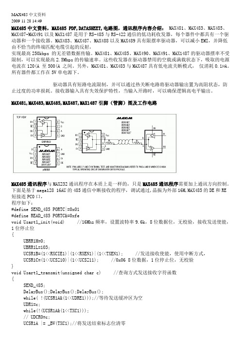
MAX481,MAX483,MAX485,MAX487,MAX1487引脚(管脚)图及工作电路MAX485通讯程序与MAX232通讯程序在本质上是一样的,只是MAX485通讯程序需要加上通讯方向控制。
下面是基于mega128 16AU的485通信中断接收的程序,调试通过,晶振为外部16M,MAX485的DE和RE短接连PC0口,程序如下:#define SEND_485 PORTC|=0x01#define READ_485 PORTC&=0xfevoid Usart1_init(void) //16Mhz频率,设置波特率9.6k,8位数据位,无校验,接收发送使能,1位停止位{UBRR1H=0;UBRR1L=103;UCSR1B=(1<<RXCIE1)|(1<<RXEN1)|(1<<TXEN1); //发送接收使能,使用中断方式,UCSR1C=(1<<UCSZ10)|(1<<UCSZ11); //0x06 8位数据,1位停止位,无校验}void Usart1_transmit(unsigned char c) //查询方式发送接收字符函数{SEND_485;DelayBus();DelayBus();DelayBus();while( !(UCSR1A&(1<<UDRE1)));//等待发送缓冲区为空UDR1=c;while(!(UCSR1A&(1<<TXC1)));// UDCR0=c;UCSR1A |= _BV(TXC1);//将发送结束标志位清零// SET_BIT(UCSR1A,);READ_485;direction++;}SIGNAL(SIG_UART1_RECV)//serial port 1 {if(UCSR1A&(1<<RXC1)){rec1buff=UDR1;rec1_flag=1;。
MAX038中文

MAX038芯片中文资料及在波形发生器中的应用(1)简介:波形发生器的应用范围很广。
在分析检测设备、超声设备、医疗设备及通讯设备中广泛应用。
函数发生器作为信号激励源,其参数精度是设计时应考虑的重要因素 ...波形发生器的应用范围很广。
在分析检测设备、超声设备、医疗设备及通讯设备中广泛应用。
函数发生器作为信号激励源,其参数精度是设计时应考虑的重要因素。
常用的波形产生电路有RC震荡电路、LC震荡电路、文氏震荡电路以及由555芯片构成的震荡电路等,但这些震荡电路由于核心芯片、选频及限幅元件特性的限制,在幅频精度方面或多或少的存在着不稳定或实现电路复杂等情况。
如果需要实现波形变换、幅频大小调整以及提高幅频的稳定度,设计的外围电路将会变得更为复杂。
由MAX038设计组成的波形产生电路能够输出幅频精度很高且易于调整的波形信号,在电路参数要求苛刻的工作场合能够得到较好的应用。
1 芯片功能介绍1.1 MAX038芯片的性能特点MAX038CPP芯片采用20引脚DIP封装,引脚图如图1所示。
各引脚功能简述如下:REF:芯片内部2.5 V参考电压输出;GND:模拟地;A1,A0:输出波形选择,TTL/CMOS兼容;COSC:内部震荡器外接电容;FADJ,DADJ:输出频率、占空比调节;IIN:震荡频率控制器电流输入;PDI,PDO:内部鉴相器输入、输出;SYNC:同步信号输出,允许内部震荡器与外电路同步;DGND,DV+:内部数字电路电源;V+,V-:MAX038电源(+5 V,-5 V);OUT:波形输出端。
MAX038芯片附加少许外围电路就能够产生三角波、锯齿波、正弦波、方波、矩形脉冲波形。
该芯片具有如下的功能特点:(1)输出频率范围:0.1~20 MHz,最高可达40 MHz:(2)输出波形占空比(15%~85%)独立可调,占空比可由DADJ端调整,如果DADJ 端接地,则输出占空比为50%;(3)具有低输出阻抗的输出缓冲器,输出阻抗的典型值为0.1 Ω;(4)备有TTL兼容的独立同步信号SYNC(方波输出,固定占空比为50%),方便组建频率合成器系统;(5)低温度漂移。
MAX6358TWUT-T中文资料
MAX6358_ _UT-T -40°C to +85°C 6 SOT23-6 MAX6359_ _UT-T -40°C to +85°C 6 SOT23-6 MAX6360_ _UT-T -40°C to +85°C 6 SOT23-6 SV 2.93 1.58 * The _ _ are placeholders for the threshold voltage levels of the UW 2.78 1.67 devices. Substitute the part number suffix in the Voltage ThresUV 2.78 1.58 hold Levels table for the desired voltage level. All devices are available in tape-and-reel only. There is a 2500 piece minimum RW 2.63 1.67 order increment for the SOT package. RV 2.63 1.58 Devices are available in both leaded and lead-free packaging. Note: Standard versions are shown in bold. Sample stock is genSpecify lead-free by replacing “-T” with “+T” when ordering. erally held on the standard versions only. Contact factory for availPin Configurations appear at end of data sheet. ability. Selector Guide appears at end of data sheet. ________________________________________________________________ Maxim Integrated Products 1
MAX485CPA+中文资料
For pricing, delivery, and ordering information,please contact Maxim/Dallas Direct!at 1-888-629-4642, or visit Maxim’s website at .General DescriptionThe MAX481, MAX483, MAX485, MAX487–MAX491, and MAX1487 are low-power transceivers for RS-485 and RS-422 communication. Each part contains one driver and one receiver. The MAX483, MAX487, MAX488, and MAX489feature reduced slew-rate drivers that minimize EMI and reduce reflections caused by improperly terminated cables,thus allowing error-free data transmission up to 250kbps.The driver slew rates of the MAX481, MAX485, MAX490,MAX491, and MAX1487 are not limited, allowing them to transmit up to 2.5Mbps.These transceivers draw between 120µA and 500µA of supply current when unloaded or fully loaded with disabled drivers. Additionally, the MAX481, MAX483, and MAX487have a low-current shutdown mode in which they consume only 0.1µA. All parts operate from a single 5V supply.Drivers are short-circuit current limited and are protected against excessive power dissipation by thermal shutdown circuitry that places the driver outputs into a high-imped-ance state. The receiver input has a fail-safe feature that guarantees a logic-high output if the input is open circuit.The MAX487 and MAX1487 feature quarter-unit-load receiver input impedance, allowing up to 128 MAX487/MAX1487 transceivers on the bus. Full-duplex communi-cations are obtained using the MAX488–MAX491, while the MAX481, MAX483, MAX485, MAX487, and MAX1487are designed for half-duplex applications.________________________ApplicationsLow-Power RS-485 Transceivers Low-Power RS-422 Transceivers Level TranslatorsTransceivers for EMI-Sensitive Applications Industrial-Control Local Area Networks__Next Generation Device Features♦For Fault-Tolerant ApplicationsMAX3430: ±80V Fault-Protected, Fail-Safe, 1/4Unit Load, +3.3V, RS-485 TransceiverMAX3440E–MAX3444E: ±15kV ESD-Protected,±60V Fault-Protected, 10Mbps, Fail-Safe, RS-485/J1708 Transceivers♦For Space-Constrained ApplicationsMAX3460–MAX3464: +5V, Fail-Safe, 20Mbps,Profibus RS-485/RS-422 TransceiversMAX3362: +3.3V, High-Speed, RS-485/RS-422Transceiver in a SOT23 PackageMAX3280E–MAX3284E: ±15kV ESD-Protected,52Mbps, +3V to +5.5V, SOT23, RS-485/RS-422,True Fail-Safe ReceiversMAX3293/MAX3294/MAX3295: 20Mbps, +3.3V,SOT23, RS-855/RS-422 Transmitters ♦For Multiple Transceiver ApplicationsMAX3030E–MAX3033E: ±15kV ESD-Protected,+3.3V, Quad RS-422 Transmitters ♦For Fail-Safe ApplicationsMAX3080–MAX3089: Fail-Safe, High-Speed (10Mbps), Slew-Rate-Limited RS-485/RS-422Transceivers♦For Low-Voltage ApplicationsMAX3483E/MAX3485E/MAX3486E/MAX3488E/MAX3490E/MAX3491E: +3.3V Powered, ±15kV ESD-Protected, 12Mbps, Slew-Rate-Limited,True RS-485/RS-422 TransceiversMAX481/MAX483/MAX485/MAX487–MAX491/MAX1487Low-Power, Slew-Rate-Limited RS-485/RS-422 Transceivers______________________________________________________________Selection Table19-0122; Rev 8; 10/03Ordering Information appears at end of data sheet.M A X 481/M A X 483/M A X 485/M A X 487–M A X 491/M A X 1487Low-Power, Slew-Rate-Limited RS-485/RS-422 Transceivers 2_______________________________________________________________________________________ABSOLUTE MAXIMUM RATINGSSupply Voltage (V CC ).............................................................12V Control Input Voltage (RE , DE)...................-0.5V to (V CC + 0.5V)Driver Input Voltage (DI).............................-0.5V to (V CC + 0.5V)Driver Output Voltage (A, B)...................................-8V to +12.5V Receiver Input Voltage (A, B).................................-8V to +12.5V Receiver Output Voltage (RO).....................-0.5V to (V CC +0.5V)Continuous Power Dissipation (T A = +70°C)8-Pin Plastic DIP (derate 9.09mW/°C above +70°C)....727mW 14-Pin Plastic DIP (derate 10.00mW/°C above +70°C)..800mW 8-Pin SO (derate 5.88mW/°C above +70°C).................471mW14-Pin SO (derate 8.33mW/°C above +70°C)...............667mW 8-Pin µMAX (derate 4.1mW/°C above +70°C)..............830mW 8-Pin CERDIP (derate 8.00mW/°C above +70°C).........640mW 14-Pin CERDIP (derate 9.09mW/°C above +70°C).......727mW Operating Temperature RangesMAX4_ _C_ _/MAX1487C_ A...............................0°C to +70°C MAX4__E_ _/MAX1487E_ A.............................-40°C to +85°C MAX4__MJ_/MAX1487MJA...........................-55°C to +125°C Storage Temperature Range.............................-65°C to +160°C Lead Temperature (soldering, 10sec).............................+300°CDC ELECTRICAL CHARACTERISTICS(V CC = 5V ±5%, T A = T MIN to T MAX , unless otherwise noted.) (Notes 1, 2)Stresses beyond those listed under “Absolute Maximum Ratings” may cause permanent damage to the device. These are stress ratings only, and functional operation of the device at these or any other conditions beyond those indicated in the operational sections of the specifications is not implied. Exposure to absolute maximum rating conditions for extended periods may affect device reliability.V V IN = -7VV IN = 12V V IN = -7V V IN = 12V Input Current (A, B)I IN2V TH k Ω48-7V ≤V CM ≤12V, MAX487/MAX1487R INReceiver Input Resistance -7V ≤V CM ≤12V, all devices except MAX487/MAX1487R = 27Ω(RS-485), Figure 40.4V ≤V O ≤2.4VR = 50Ω(RS-422)I O = 4mA, V ID = -200mV I O = -4mA, V ID = 200mV V CM = 0V-7V ≤V CM ≤12V DE, DI, RE DE, DI, RE MAX487/MAX1487,DE = 0V, V CC = 0V or 5.25VDE, DI, RE R = 27Ωor 50Ω, Figure 4R = 27Ωor 50Ω, Figure 4R = 27Ωor 50Ω, Figure 4DE = 0V;V CC = 0V or 5.25V,all devices except MAX487/MAX1487CONDITIONSk Ω12µA ±1I OZRThree-State (high impedance)Output Current at ReceiverV 0.4V OL Receiver Output Low Voltage 3.5V OH Receiver Output High Voltage mV 70∆V TH Receiver Input Hysteresis V -0.20.2Receiver Differential Threshold Voltage-0.2mA 0.25mA-0.81.01.55V OD2Differential Driver Output (with load)V 2V 5V OD1Differential Driver Output (no load)µA±2I IN1Input CurrentV 0.8V IL Input Low Voltage V 2.0V IH Input High Voltage V 0.2∆V OD Change in Magnitude of Driver Common-Mode Output Voltage for Complementary Output States V 0.2∆V OD Change in Magnitude of Driver Differential Output Voltage for Complementary Output States V 3V OC Driver Common-Mode Output VoltageUNITS MINTYPMAX SYMBOL PARAMETERMAX481/MAX483/MAX485/MAX487–MAX491/MAX1487Low-Power, Slew-Rate-Limited RS-485/RS-422 Transceivers_______________________________________________________________________________________3SWITCHING CHARACTERISTICS—MAX481/MAX485, MAX490/MAX491, MAX1487(V CC = 5V ±5%, T A = T MIN to T MAX , unless otherwise noted.) (Notes 1, 2)DC ELECTRICAL CHARACTERISTICS (continued)(V CC = 5V ±5%, T A = T MIN to T MAX , unless otherwise noted.) (Notes 1, 2)ns 103060t PHLDriver Rise or Fall Time Figures 6 and 8, R DIFF = 54Ω, C L1= C L2= 100pF ns MAX490M, MAX491M MAX490C/E, MAX491C/E2090150MAX481, MAX485, MAX1487MAX490M, MAX491MMAX490C/E, MAX491C/E MAX481, MAX485, MAX1487Figures 6 and 8, R DIFF = 54Ω,C L1= C L2= 100pF MAX481 (Note 5)Figures 5 and 11, C RL = 15pF, S2 closedFigures 5 and 11, C RL = 15pF, S1 closed Figures 5 and 11, C RL = 15pF, S2 closed Figures 5 and 11, C RL = 15pF, S1 closed Figures 6 and 10, R DIFF = 54Ω,C L1= C L2= 100pFFigures 6 and 8,R DIFF = 54Ω,C L1= C L2= 100pF Figures 6 and 10,R DIFF = 54Ω,C L1= C L2= 100pF CONDITIONS ns 510t SKEW ns50200600t SHDNTime to ShutdownMbps 2.5f MAX Maximum Data Rate ns 2050t HZ Receiver Disable Time from High ns 103060t PLH 2050t LZ Receiver Disable Time from Low ns 2050t ZH Driver Input to Output Receiver Enable to Output High ns 2050t ZL Receiver Enable to Output Low 2090200ns ns 134070t HZ t SKD Driver Disable Time from High |t PLH - t PHL |DifferentialReceiver Skewns 4070t LZ Driver Disable Time from Low ns 4070t ZL Driver Enable to Output Low 31540ns51525ns 31540t R , t F 2090200Driver Output Skew to Output t PLH , t PHL Receiver Input to Output4070t ZH Driver Enable to Output High UNITS MIN TYP MAX SYMBOL PARAMETERFigures 7 and 9, C L = 100pF, S2 closed Figures 7 and 9, C L = 100pF, S1 closed Figures 7 and 9, C L = 15pF, S1 closed Figures 7 and 9, C L = 15pF, S2 closedM A X 481/M A X 483/M A X 485/M A X 487–M A X 491/M A X 1487Low-Power, Slew-Rate-Limited RS-485/RS-422 Transceivers 4_______________________________________________________________________________________SWITCHING CHARACTERISTICS—MAX483, MAX487/MAX488/MAX489(V CC = 5V ±5%, T A = T MIN to T MAX , unless otherwise noted.) (Notes 1, 2)SWITCHING CHARACTERISTICS—MAX481/MAX485, MAX490/MAX491, MAX1487 (continued)(V CC = 5V ±5%, T A = T MIN to T MAX , unless otherwise noted.) (Notes 1, 2)3001000Figures 7 and 9, C L = 100pF, S2 closed Figures 7 and 9, C L = 100pF, S1 closed Figures 5 and 11, C L = 15pF, S2 closed,A - B = 2VCONDITIONSns 40100t ZH(SHDN)Driver Enable from Shutdown toOutput High (MAX481)nsFigures 5 and 11, C L = 15pF, S1 closed,B - A = 2Vt ZL(SHDN)Receiver Enable from Shutdownto Output Low (MAX481)ns 40100t ZL(SHDN)Driver Enable from Shutdown toOutput Low (MAX481)ns 3001000t ZH(SHDN)Receiver Enable from Shutdownto Output High (MAX481)UNITS MINTYP MAX SYMBOLPARAMETERt PLH t SKEW Figures 6 and 8, R DIFF = 54Ω,C L1= C L2= 100pFt PHL Figures 6 and 8, R DIFF = 54Ω,C L1= C L2= 100pFDriver Input to Output Driver Output Skew to Output ns 100800ns ns 2000MAX483/MAX487, Figures 7 and 9,C L = 100pF, S2 closedt ZH(SHDN)Driver Enable from Shutdown to Output High2502000ns2500MAX483/MAX487, Figures 5 and 11,C L = 15pF, S1 closedt ZL(SHDN)Receiver Enable from Shutdown to Output Lowns 2500MAX483/MAX487, Figures 5 and 11,C L = 15pF, S2 closedt ZH(SHDN)Receiver Enable from Shutdown to Output Highns 2000MAX483/MAX487, Figures 7 and 9,C L = 100pF, S1 closedt ZL(SHDN)Driver Enable from Shutdown to Output Lowns 50200600MAX483/MAX487 (Note 5) t SHDN Time to Shutdownt PHL t PLH , t PHL < 50% of data period Figures 5 and 11, C RL = 15pF, S2 closed Figures 5 and 11, C RL = 15pF, S1 closed Figures 5 and 11, C RL = 15pF, S2 closed Figures 5 and 11, C RL = 15pF, S1 closed Figures 7 and 9, C L = 15pF, S2 closed Figures 6 and 10, R DIFF = 54Ω,C L1= C L2= 100pFFigures 7 and 9, C L = 15pF, S1 closed Figures 7 and 9, C L = 100pF, S1 closed Figures 7 and 9, C L = 100pF, S2 closed CONDITIONSkbps 250f MAX 2508002000Maximum Data Rate ns 2050t HZ Receiver Disable Time from High ns 25080020002050t LZ Receiver Disable Time from Low ns 2050t ZH Receiver Enable to Output High ns 2050t ZL Receiver Enable to Output Low ns ns 1003003000t HZ t SKD Driver Disable Time from High I t PLH - t PHL I DifferentialReceiver SkewFigures 6 and 10, R DIFF = 54Ω,C L1= C L2= 100pFns 3003000t LZ Driver Disable Time from Low ns 2502000t ZL Driver Enable to Output Low ns Figures 6 and 8, R DIFF = 54Ω,C L1= C L2= 100pFns 2502000t R , t F 2502000Driver Rise or Fall Time ns t PLH Receiver Input to Output2502000t ZH Driver Enable to Output High UNITS MIN TYP MAX SYMBOL PARAMETERMAX481/MAX483/MAX485/MAX487–MAX491/MAX1487Low-Power, Slew-Rate-Limited RS-485/RS-422 Transceivers_______________________________________________________________________________________530002.5OUTPUT CURRENT vs.RECEIVER OUTPUT LOW VOLTAGE525M A X 481-01OUTPUT LOW VOLTAGE (V)O U T P U T C U R R E N T (m A )1.515100.51.02.0203540450.90.1-50-252575RECEIVER OUTPUT LOW VOLTAGE vs.TEMPERATURE0.30.7TEMPERATURE (°C)O U T P U TL O W V O L T A G E (V )500.50.80.20.60.40100125-20-41.5 2.0 3.0 5.0OUTPUT CURRENT vs.RECEIVER OUTPUT HIGH VOLTAGE-8-16M A X 481-02OUTPUT HIGH VOLTAGE (V)O U T P U T C U R R E N T (m A )2.5 4.0-12-18-6-14-10-203.54.5 4.83.2-50-252575RECEIVER OUTPUT HIGH VOLTAGE vs.TEMPERATURE3.64.4TEMPERATURE (°C)O U T P UT H I G H V O L T A G E (V )0504.04.63.44.23.83.01001259000 1.0 3.0 4.5DRIVER OUTPUT CURRENT vs.DIFFERENTIAL OUTPUT VOLTAGE1070M A X 481-05DIFFERENTIAL OUTPUT VOLTAGE (V)O U T P U T C U R R E N T (m A )2.0 4.05030806040200.5 1.5 2.53.5 2.31.5-50-2525125DRIVER DIFFERENTIAL OUTPUT VOLTAGEvs. TEMPERATURE1.72.1TEMPERATURE (°C)D I F FE R E N T I A L O U T P U T V O L T A G E (V )751.92.21.62.01.8100502.4__________________________________________Typical Operating Characteristics(V CC = 5V, T A = +25°C, unless otherwise noted.)NOTES FOR ELECTRICAL/SWITCHING CHARACTERISTICSNote 1:All currents into device pins are positive; all currents out of device pins are negative. All voltages are referenced to deviceground unless otherwise specified.Note 2:All typical specifications are given for V CC = 5V and T A = +25°C.Note 3:Supply current specification is valid for loaded transmitters when DE = 0V.Note 4:Applies to peak current. See Typical Operating Characteristics.Note 5:The MAX481/MAX483/MAX487 are put into shutdown by bringing RE high and DE low. If the inputs are in this state for lessthan 50ns, the parts are guaranteed not to enter shutdown. If the inputs are in this state for at least 600ns, the parts are guaranteed to have entered shutdown. See Low-Power Shutdown Mode section.M A X 481/M A X 483/M A X 485/M A X 487–M A X 491/M A X 1487Low-Power, Slew-Rate-Limited RS-485/RS-422 Transceivers 6___________________________________________________________________________________________________________________Typical Operating Characteristics (continued)(V CC = 5V, T A = +25°C, unless otherwise noted.)120008OUTPUT CURRENT vs.DRIVER OUTPUT LOW VOLTAGE20100M A X 481-07OUTPUT LOW VOLTAGE (V)O U T P U T C U R R E N T (m A )6604024801012140-1200-7-5-15OUTPUT CURRENT vs.DRIVER OUTPUT HIGH VOLTAGE-20-80M A X 481-08OUTPUT HIGH VOLTAGE (V)O U T P U T C U R R E N T (m A )-31-603-6-4-2024-100-40100-40-60-2040100120MAX1487SUPPLY CURRENT vs. TEMPERATURE300TEMPERATURE (°C)S U P P L Y C U R R E N T (µA )20608050020060040000140100-50-2550100MAX481/MAX485/MAX490/MAX491SUPPLY CURRENT vs. TEMPERATURE300TEMPERATURE (°C)S U P P L Y C U R R E N T (µA )257550020060040000125100-50-2550100MAX483/MAX487–MAX489SUPPLY CURRENT vs. TEMPERATURE300TEMPERATURE (°C)S U P P L Y C U R R E N T (µA )257550020060040000125MAX481/MAX483/MAX485/MAX487–MAX491/MAX1487Low-Power, Slew-Rate-Limited RS-485/RS-422 Transceivers_______________________________________________________________________________________7______________________________________________________________Pin DescriptionFigure 1. MAX481/MAX483/MAX485/MAX487/MAX1487 Pin Configuration and Typical Operating CircuitM A X 481/M A X 483/M A X 485/M A X 487–M A X 491/M A X 1487__________Applications InformationThe MAX481/MAX483/MAX485/MAX487–MAX491 and MAX1487 are low-power transceivers for RS-485 and RS-422 communications. The MAX481, MAX485, MAX490,MAX491, and MAX1487 can transmit and receive at data rates up to 2.5Mbps, while the MAX483, MAX487,MAX488, and MAX489 are specified for data rates up to 250kbps. The MAX488–MAX491 are full-duplex trans-ceivers while the MAX481, MAX483, MAX485, MAX487,and MAX1487 are half-duplex. In addition, Driver Enable (DE) and Receiver Enable (RE) pins are included on the MAX481, MAX483, MAX485, MAX487, MAX489,MAX491, and MAX1487. When disabled, the driver and receiver outputs are high impedance.MAX487/MAX1487:128 Transceivers on the BusThe 48k Ω, 1/4-unit-load receiver input impedance of the MAX487 and MAX1487 allows up to 128 transceivers on a bus, compared to the 1-unit load (12k Ωinput impedance) of standard RS-485 drivers (32 trans-ceivers maximum). Any combination of MAX487/MAX1487 and other RS-485 transceivers with a total of 32 unit loads or less can be put on the bus. The MAX481/MAX483/MAX485 and MAX488–MAX491 have standard 12k ΩReceiver Input impedance.Low-Power, Slew-Rate-Limited RS-485/RS-422 Transceivers 8_______________________________________________________________________________________Figure 2. MAX488/MAX490 Pin Configuration and Typical Operating CircuitFigure 3. MAX489/MAX491 Pin Configuration and Typical Operating CircuitMAX483/MAX487/MAX488/MAX489:Reduced EMI and ReflectionsThe MAX483 and MAX487–MAX489 are slew-rate limit-ed, minimizing EMI and reducing reflections caused by improperly terminated cables. Figure 12 shows the dri-ver output waveform and its Fourier analysis of a 150kHz signal transmitted by a MAX481, MAX485,MAX490, MAX491, or MAX1487. High-frequency har-monics with large amplitudes are evident. Figure 13shows the same information displayed for a MAX483,MAX487, MAX488, or MAX489 transmitting under the same conditions. Figure 13’s high-frequency harmonics have much lower amplitudes, and the potential for EMI is significantly reduced.MAX481/MAX483/MAX485/MAX487–MAX491/MAX1487Low-Power, Slew-Rate-Limited RS-485/RS-422 Transceivers_______________________________________________________________________________________9_________________________________________________________________Test CircuitsFigure 4. Driver DC Test Load Figure 5. Receiver Timing Test LoadFigure 6. Driver/Receiver Timing Test Circuit Figure 7. Driver Timing Test LoadM A X 481/M A X 483/M A X 485/M A X 487–M A X 491/M A X 1487Low-Power, Slew-Rate-Limited RS-485/RS-422 Transceivers 10_______________________________________________________Switching Waveforms_________________Function Tables (MAX481/MAX483/MAX485/MAX487/MAX1487)Figure 8. Driver Propagation DelaysFigure 9. Driver Enable and Disable Times (except MAX488 and MAX490)Figure 10. Receiver Propagation DelaysFigure 11. Receiver Enable and Disable Times (except MAX488and MAX490)Table 1. TransmittingTable 2. ReceivingLow-Power Shutdown Mode (MAX481/MAX483/MAX487)A low-power shutdown mode is initiated by bringing both RE high and DE low. The devices will not shut down unless both the driver and receiver are disabled.In shutdown, the devices typically draw only 0.1µA of supply current.RE and DE may be driven simultaneously; the parts are guaranteed not to enter shutdown if RE is high and DE is low for less than 50ns. If the inputs are in this state for at least 600ns, the parts are guaranteed to enter shutdown.For the MAX481, MAX483, and MAX487, the t ZH and t ZL enable times assume the part was not in the low-power shutdown state (the MAX485/MAX488–MAX491and MAX1487 can not be shut down). The t ZH(SHDN)and t ZL(SHDN)enable times assume the parts were shut down (see Electrical Characteristics ).It takes the drivers and receivers longer to become enabled from the low-power shutdown state (t ZH(SHDN ), t ZL(SHDN)) than from the operating mode (t ZH , t ZL ). (The parts are in operating mode if the –R —E –,DE inputs equal a logical 0,1 or 1,1 or 0, 0.)Driver Output ProtectionExcessive output current and power dissipation caused by faults or by bus contention are prevented by two mechanisms. A foldback current limit on the output stage provides immediate protection against short cir-cuits over the whole common-mode voltage range (see Typical Operating Characteristics ). In addition, a ther-mal shutdown circuit forces the driver outputs into a high-impedance state if the die temperature rises excessively.Propagation DelayMany digital encoding schemes depend on the differ-ence between the driver and receiver propagation delay times. Typical propagation delays are shown in Figures 15–18 using Figure 14’s test circuit.The difference in receiver delay times, | t PLH - t PHL |, is typically under 13ns for the MAX481, MAX485,MAX490, MAX491, and MAX1487 and is typically less than 100ns for the MAX483 and MAX487–MAX489.The driver skew times are typically 5ns (10ns max) for the MAX481, MAX485, MAX490, MAX491, and MAX1487, and are typically 100ns (800ns max) for the MAX483 and MAX487–MAX489.MAX481/MAX483/MAX485/MAX487–MAX491/MAX1487Low-Power, Slew-Rate-Limited RS-485/RS-422 Transceivers______________________________________________________________________________________1110dB/div0Hz5MHz500kHz/div10dB/div0Hz5MHz500kHz/divFigure 12. Driver Output Waveform and FFT Plot of MAX481/MAX485/MAX490/MAX491/MAX1487 Transmitting a 150kHz SignalFigure 13. Driver Output Waveform and FFT Plot of MAX483/MAX487–MAX489 Transmitting a 150kHz SignalM A X 481/M A X 483/M A X 485/M A X 487–M A X 491/M A X 1487Low-Power, Slew-Rate-Limited RS-485/RS-422 Transceivers 12______________________________________________________________________________________V CC = 5V T A = +25°CV CC = 5V T A = +25°CV CC = 5V T A = +25°CV CC = 5V T A = +25°CFigure 14. Receiver Propagation Delay Test CircuitFigure 15. MAX481/MAX485/MAX490/MAX491/MAX1487Receiver t PHLFigure 16. MAX481/MAX485/MAX490/MAX491/MAX1487Receiver t PLHPHL Figure 18. MAX483, MAX487–MAX489 Receiver t PLHLine Length vs. Data RateThe RS-485/RS-422 standard covers line lengths up to 4000 feet. For line lengths greater than 4000 feet, see Figure 23.Figures 19 and 20 show the system differential voltage for the parts driving 4000 feet of 26AWG twisted-pair wire at 110kHz into 120Ωloads.Typical ApplicationsThe MAX481, MAX483, MAX485, MAX487–MAX491, and MAX1487 transceivers are designed for bidirectional data communications on multipoint bus transmission lines.Figures 21 and 22 show typical network applications circuits. These parts can also be used as line repeaters, with cable lengths longer than 4000 feet, as shown in Figure 23.To minimize reflections, the line should be terminated at both ends in its characteristic impedance, and stub lengths off the main line should be kept as short as possi-ble. The slew-rate-limited MAX483 and MAX487–MAX489are more tolerant of imperfect termination.MAX481/MAX483/MAX485/MAX487–MAX491/MAX1487Low-Power, Slew-Rate-Limited RS-485/RS-422 Transceivers______________________________________________________________________________________13DIV Y -V ZRO5V 0V1V0V -1V5V 0V2µs/divFigure 19. MAX481/MAX485/MAX490/MAX491/MAX1487 System Differential Voltage at 110kHz Driving 4000ft of Cable Figure 20. MAX483, MAX487–MAX489 System Differential Voltage at 110kHz Driving 4000ft of CableFigure 21. MAX481/MAX483/MAX485/MAX487/MAX1487 Typical Half-Duplex RS-485 NetworkM A X 481/M A X 483/M A X 485/M A X 487–M A X 491/M A X 1487Low-Power, Slew-Rate-Limited RS-485/RS-422 Transceivers 14______________________________________________________________________________________Figure 22. MAX488–MAX491 Full-Duplex RS-485 NetworkFigure 23. Line Repeater for MAX488–MAX491Isolated RS-485For isolated RS-485 applications, see the MAX253 and MAX1480 data sheets.MAX481/MAX483/MAX485/MAX487–MAX491/MAX1487Low-Power, Slew-Rate-Limited RS-485/RS-422 Transceivers______________________________________________________________________________________15_______________Ordering Information_________________Chip TopographiesMAX481/MAX483/MAX485/MAX487/MAX1487N.C. RO 0.054"(1.372mm)0.080"(2.032mm)DE DIGND B N.C.V CCARE * Contact factory for dice specifications.__Ordering Information (continued)M A X 481/M A X 483/M A X 485/M A X 487–M A X 491/M A X 1487Low-Power, Slew-Rate-Limited RS-485/RS-422 Transceivers 16______________________________________________________________________________________TRANSISTOR COUNT: 248SUBSTRATE CONNECTED TO GNDMAX488/MAX490B RO 0.054"(1.372mm)0.080"(2.032mm)N.C. DIGND Z A V CCYN.C._____________________________________________Chip Topographies (continued)MAX489/MAX491B RO 0.054"(1.372mm)0.080"(2.032mm)DE DIGND Z A V CCYREMAX481/MAX483/MAX485/MAX487–MAX491/MAX1487Low-Power, Slew-Rate-Limited RS-485/RS-422 Transceivers______________________________________________________________________________________17Package Information(The package drawing(s) in this data sheet may not reflect the most current specifications. For the latest package outline information go to /packages .)S O I C N .E P SM A X 481/M A X 483/M A X 485/M A X 487–M A X 491/M A X 1487Low-Power, Slew-Rate-Limited RS-485/RS-422 Transceivers 18______________________________________________________________________________________Package Information (continued)(The package drawing(s) in this data sheet may not reflect the most current specifications. For the latest package outline information go to /packages .)MAX481/MAX483/MAX485/MAX487–MAX491Low-Power, Slew-Rate-Limited RS-485/RS-422 TransceiversMaxim cannot assume responsibility for use of any circuitry other than circuitry entirely embodied in a Maxim product. No circuit patent licenses are implied. Maxim reserves the right to change the circuitry and specifications without notice at any time.Maxim Integrated Products, 120 San Gabriel Drive, Sunnyvale, CA 94086 408-737-7600 ____________________19©2003 Maxim Integrated ProductsPrinted USAis a registered trademark of Maxim Integrated Products.M A X 481/M A X 483/M A X 485/M A X 487–M A X 491/M A X 1487P D I P N .E PSPackage Information (continued)(The package drawing(s) in this data sheet may not reflect the most current specifications. For the latest package outline information go to /packages .)。
NI 6358 X Series数据收集设备规格说明书

DEVICE SPECIFICATIONSNI 6358X Series Data Acquisition: 1.25 MS/s/ch, 16 AI, 48 DIO, 4 AOThe following specifications are typical at 25 °C, unless otherwise noted. For more information about the NI 6358, refer to the X Series User Manual available from / manuals.Analog InputNumber of channels16 differentialADC resolution16 bitsDNL No missing codes guaranteedINL Refer to the AI Absolute Accuracy section. Sample rateSingle channel maximum 1.25 MS/sMinimum No minimumTiming resolution10 nsTiming accuracy50 ppm of sample rateInput coupling DCInput range±1 V, ±2 V, ±5 V, ±10 VMaximum working voltage for all analog inputsPositive input (AI+)±11 V for all ranges, Measurement Category I Negative input (AI-)±11 V for all ranges, Measurement Category I Caution Do not use for measurements within Categories II, III, and IV.CMRR (at 60 Hz)75 dBBandwidth 1 MHzTHD-80 dBFSInput impedanceDevice onAI+ to AI GND>100 GΩ in parallel with 100 pFAI- to AI GND>100 GΩ in parallel with 100 pF Device offAI+ to AI GND 2 kΩAI- to AI GND 2 kΩInput bias current±10 pACrosstalk (at 100 kHz)Adjacent channels-80 dBNon-adjacent channels-100 dBInput FIFO size8,182 samples shared among channels used Data transfers DMA (scatter-gather), programmed I/O Overvoltage protection for all analog input channelsDevice on±36 VDevice off±15 VInput current during overvoltage±20 mA max/AI pinconditionsAnalog T riggersNumber of triggers1Source AI <0..15>, APFI <0, 1>Functions Start Trigger, Reference Trigger, PauseTrigger, Sample Clock, Sample ClockTimebaseSource levelAI <0..15>±Full scaleAPFI <0, 1>±10 VResolution16 bitsModes Analog edge triggering, analog edge triggeringwith hysteresis, and analog window triggering 2| | NI 6358 Device SpecificationsBandwidth (-3 dB)AI <0..15> 3.4 MHzAPFI <0, 1> 3.9 MHz Accuracy±1% of range APFI <0, 1> characteristicsInput impedance10 kΩCoupling DCProtection, power on±30 VProtection, power off±15 VAI Absolute AccuracyNote For more information about absolute accuracy at full scale, refer to the AIAbsolute Accuracy Example section.Gain tempco8 ppm/°CReference tempco 5 ppm/°CResidual offset error15 ppm of rangeINL error46 ppm of rangeNote Accuracies listed are valid for up to two years from the device externalcalibration.AI Absolute Accuracy EquationAbsoluteAccuracy = Reading · (GainError) + Range · (OffsetError) + NoiseUncertainty GainError = ResidualGainError + GainTempco · (TempChangeFromLastInternalCal) + ReferenceTempco · (TempChangeFromLastExternalCal)NI 6358 Device Specifications| © National Instruments| 3OffsetError = ResidualOffsetError + OffsetTempco · (TempChangeFromLastInternalCal) + INLErrorNoiseUncertainty10,000 points.AI Absolute Accuracy ExampleAbsolute accuracy at full scale on the analog input channels is determined using the following assumptions:•TempChangeFromLastExternalCal = 10 °C •TempChangeFromLastInternalCal = 1 °C•number_of_readings = 10,000•CoverageFactor = 3 σFor example, on the 10 V range, the absolute accuracy at full scale is as follows: GainError = 114 ppm + 8 ppm · 1 + 5 ppm · 10 = 172 ppmOffsetError = 15 ppm + 35 ppm ·1 + 46 ppm = 96 ppmNoise UncertaintyAbsoluteAccuracy = 10 V · (GainError) + 10 V · (OffsetError) + NoiseUncertainty = 2688 µVAnalog OutputNumber of channels4DAC resolution16 bitsDNL±1 LSB, maxMonotonicity16 bit guaranteedAccuracy Refer to the AO Absolute Accuracy section. Maximum update rate (simultaneous)1 channel 3.3 MS/s2 channels 3.3 MS/s3 channels 3.3 MS/s4 channels 3.3 MS/sMinimum update rate No minimumTiming accuracy50 ppm of sample rateTiming resolution10 ns4| | NI 6358 Device SpecificationsOutput range±10 V, ±5 V, ±external reference onAPFI <0, 1>Output coupling DCOutput impedance0.4 ΩOutput current drive±5 mAOverdrive protection±25 VOverdrive current10 mAPower-on state±5 mVPower-on/off glitch 1.5 V peak for 200 msOutput FIFO size8,191 samples shared among channels used Data transfers DMA (scatter-gather), programmed I/OAO waveform modes Non-periodic waveform, periodic waveformregeneration mode from onboard FIFO,periodic waveform regeneration from hostbuffer including dynamic update2 µsSettling time, full-scale step,15 ppm (1 LSB)Slew rate20 V/µs6 nV · sGlitch energy at midscale transition,±10 V rangeExternal ReferenceAPFI <0, 1> characteristicsInput impedance10 kΩCoupling DCProtection, device on± 30 VProtection, device off± 15 VRange± 11 VSlew rate20 V/μsNI 6358 Device Specifications| © National Instruments| 5Figure 1. Analog Output External Reference Bandwidth–90–80–70–60–50–40–30–20–10010Frequency (Hz)N o r m a l i z e d A O A m p l i t u d e A t t e n u a t i o n (d B )AO Absolute AccuracyAbsolute accuracy at full-scale numbers is valid immediately following self calibration and assumes the device is operating within 10 °C of the last external calibration.Note Accuracies listed are valid for up to two years from the device externalcalibration.AO Absolute Accuracy EquationAbsoluteAccuracy = OutputValue ⋅ (GainError ) + Range ⋅ (OffsetError )GainError = ResidualGainError + GainTempco ⋅ (TempChangeFromLastInternalCal ) +ReferenceTempco ⋅ (TempChangeFromLastExternalCal )OffsetError = ResidualOffsetError + OffsetTempco ⋅ (TempChangeFromLastInternalCal )+ INLError6 | | NI 6358 Device SpecificationsDigital I/O/PFIStatic CharacteristicsNumber of channels48 total, 32 (P0.<0..31>,16 (PFI <0..7>/P1, PFI <8..15>/P2)Ground reference D GNDDirection control Each terminal individually programmable asinput or outputPull-down resistor50 kΩ typical, 20 kΩ minimumInput voltage protection±20 V on up to two pinsCaution Stresses beyond those listed under the Input voltage protectionspecification may cause permanent damage to the device.Waveform Characteristics (Port 0 Only)Terminals used Port 0 (P0.<0..31>)Port/sample size Up to 32 bitsWaveform generation (DO) FIFO2,047 samplesWaveform acquisition (DI) FIFO255 samplesDI Sample Clock frequency0 to 10 MHz, system and bus activitydependentDO Sample Clock frequencyRegenerate from FIFO0 to 10 MHzStreaming from memory0 to 10 MHz, system and bus activitydependentData transfers DMA (scatter-gather), programmed I/O Digital line filter settings160 ns, 10.24 μs, 5.12 ms, disablePFI/Port 1/Port 2 FunctionalityFunctionality Static digital input, static digital output, timinginput, timing outputTiming output sources Many AI, AO, counter, DI, DO timing signals Debounce filter settings90 ns, 5.12 µs, 2.56 ms, custom interval,disable; programmable high and lowtransitions; selectable per inputNI 6358 Device Specifications| © National Instruments| 7Recommended Operating Conditions Input high voltage (V IH)Minimum 2.2 VMaximum 5.25 VInput low voltage (V IL)Minimum0 VMaximum0.8 VOutput high current (I OH)P0.<0..7>-24 mA maximum PFI <0..15>/P1/P2-16 mA maximum Output low current (I OL)P0.<0..7>24 mA maximum PFI <0..15>/P1/P216 mA maximum Digital I/O CharacteristicsPositive-going threshold (VT+) 2.2 V maximum Negative-going threshold (VT-)0.8 V minimum Delta VT hysteresis (VT+ - VT-)0.2 V minimum I IL input low current (V IN = 0 V)-10 μA maximum I IH input high current (V IN = 5 V)250 μA maximum8| | NI 6358 Device SpecificationsFigure 2. P0.<0..31>: I OH versus V OHI O H (m A )–30–5–10–15–20–25–35–40–45V OH (V)0–50Figure 3. P0.<0..31>: I OL versus VOLI O L (m A )1535302520105V OL (V)400NI 6358 Device Specifications | © National Instruments | 9Figure 4. PFI <0..15>/P1/P2: I OH versus V OHI O H (m A )–30–5–10–15–20–25–35–40–45V OH (V)0–50Figure 5. PFI <0..15>/P1/P2: I OL versus V OLI O L (m A )5V OL (V)0General-Purpose CountersNumber of counter/timers 4Resolution32 bits10 | | NI 6358 Device SpecificationsCounter measurements Edge counting, pulse, pulse width,semi-period, period, two-edge separation Position measurements X1, X2, X4 quadrature encoding withChannel Z reloading; two-pulse encoding Output applications Pulse, pulse train with dynamic updates,frequency division, equivalent time sampling Internal base clocks100 MHz, 20 MHz, 100 kHzExternal base clock frequency0 MHz to 25 MHz; 0 MHz to 100 MHz onPXIe_DSTAR<A,B>Base clock accuracy50 ppmInputs Gate, Source, HW_Arm, Aux, A, B, Z,Up_Down, Sample ClockRouting options for inputs Any PFI, PXIe_DSTAR<A,B>, PXI_TRIG,PXI_STAR, analog trigger, many internaltriggersFIFO127 samples per counterData transfers Dedicated scatter-gather DMA controller foreach counter/timer, programmed I/OFrequency GeneratorNumber of channels1Base clocks20 MHz, 10 MHz, 100 kHzDivisors 1 to 16Base clock accuracy50 ppmOutput can be available on any PFI terminal.Phase-Locked Loop (PLL)Number of PLLs1NI 6358 Device Specifications| © National Instruments| 11Table 3. Reference Clock Locking Frequencies (Continued)Output of PLL100 MHz Timebase; other signals derived from100 MHz Timebase including 20 MHz and100 kHz TimebasesExternal Digital TriggersSource Any PFI, PXIe_DSTAR<A,B>, PXI_TRIG,PXI_STARPolarity Software-selectable for most signalsAnalog input function Start Trigger, Reference Trigger, PauseTrigger, Sample Clock, Convert Clock, SampleClock TimebaseAnalog output function Start Trigger, Pause Trigger, Sample Clock,Sample Clock TimebaseCounter/timer functions Gate, Source, HW_Arm, Aux, A, B, Z,Up_Down, Sample ClockDigital waveform generation (DO) function Start Trigger, Pause Trigger, Sample Clock, Sample Clock TimebaseDigital waveform acquisition (DI) function Start Trigger, Reference Trigger, Pause Trigger, Sample Clock, Sample Clock TimebaseDevice-to-Device T rigger BusInput source PXI_TRIG <0..7>, PXI_STAR,PXIe_DSTAR<A,B>Output destination PXI_TRIG <0..7>, PXIe_DSTARC 12| | NI 6358 Device SpecificationsOutput selections10 MHz Clock, frequency generator output,many internal signalsDebounce filter settings90 ns, 5.12 μs, 2.56 ms, custom interval,disable; programmable high and lowtransitions; selectable per inputBus InterfaceForm factor x1 PXI Express peripheral module,specification rev 1.0 compliantSlot compatibility x1 and x4 PXI Express or PXI Express hybridslotsDMA channels8, can be used for analog input, analog output,digital input, digital output, counter/timer 0,counter/timer 1, counter/timer 2,counter/timer 3All PXIe devices may be installed in PXI Express slots or PXI Express hybrid slots.Power RequirementsCaution The protection provided by the device can be impaired if the device isused in a manner not described in the X Series User Manual.PXIe+3.3 V7.8 W+12 V22.2 WCurrent LimitsCaution Exceeding the current limits may cause unpredictable device behavior.+5 V terminal (connector 0) 1 A max1+5 V terminal (connector 1) 1 A max11.8 A maxP0/PFI/P1/P2 and +5 V terminalscombined1Has a self-resetting fuse that opens when current exceeds this specification.NI 6358 Device Specifications| © National Instruments| 13Physical CharacteristicsPXIe printed circuit board dimensions Standard 3U PXIWeight241 g (8.5 oz)I/O connectors 2 68-pin VHDCI16-24 AWGUSB screw terminal/BNC screw terminalwiringCalibrationRecommended warm-up time15 minutesCalibration interval 2 yearsMaximum Working VoltageMaximum working voltage refers to the signal voltage plus the common-mode voltage. Channel to earth11 V, Measurement Category I Caution Do not use for measurements within Categories II, III, or IV.14| | NI 6358 Device SpecificationsShock and VibrationOperational shock30 g peak, half-sine, 11 ms pulse(Tested in accordance with IEC 60068-2-27.Test profile developed in accordance withMIL-PRF-28800F.)Random vibrationOperating 5 to 500 Hz, 0.3 g rmsNonoperating 5 to 500 Hz, 2.4 g rms(Tested in accordance with IEC 60068-2-64.Nonoperating test profile exceeds therequirements of MIL-PRF-28800F, Class 3.)EnvironmentalOperating temperature0 to 55 ºCStorage temperature-40 to 70 ºCOperating humidity10 to 90% RH, noncondensingStorage humidity 5 to 95% RH, noncondensingPollution Degree2Maximum altitude2,000 mIndoor use only.SafetyThis product is designed to meet the requirements of the following electrical equipment safety standards for measurement, control, and laboratory use:•IEC 61010-1, EN 61010-1•UL 61010-1, CSA 61010-1Note For UL and other safety certifications, refer to the product label or the OnlineProduct Certification section.Electromagnetic CompatibilityThis product meets the requirements of the following EMC standards for electrical equipment for measurement, control, and laboratory use:•EN 61326-1 (IEC 61326-1): Class A emissions; Basic immunity•EN 55011 (CISPR 11): Group 1, Class A emissionsNI 6358 Device Specifications| © National Instruments| 15•EN 55022 (CISPR 22): Class A emissions•EN 55024 (CISPR 24): Immunity•AS/NZS CISPR 11: Group 1, Class A emissions•AS/NZS CISPR 22: Class A emissions•FCC 47 CFR Part 15B: Class A emissions•ICES-001: Class A emissionsNote In the United States (per FCC 47 CFR), Class A equipment is intended foruse in commercial, light-industrial, and heavy-industrial locations. In Europe,Canada, Australia and New Zealand (per CISPR 11) Class A equipment is intendedfor use only in heavy-industrial locations.Note Group 1 equipment (per CISPR 11) is any industrial, scientific, or medicalequipment that does not intentionally generate radio frequency energy for thetreatment of material or inspection/analysis purposes.Note For EMC declarations and certifications, and additional information, refer tothe Online Product Certification section.CE ComplianceThis product meets the essential requirements of applicable European Directives, as follows:•2014/35/EU; Low-V oltage Directive (safety)•2014/30/EU; Electromagnetic Compatibility Directive (EMC)Online Product CertificationRefer to the product Declaration of Conformity (DoC) for additional regulatory compliance information. To obtain product certifications and the DoC for this product, visit / certification, search by model number or product line, and click the appropriate link in the Certification column.Environmental ManagementNI is committed to designing and manufacturing products in an environmentally responsible manner. NI recognizes that eliminating certain hazardous substances from our products is beneficial to the environment and to NI customers.For additional environmental information, refer to the Minimize Our Environmental Impact web page at /environment. This page contains the environmental regulations and directives with which NI complies, as well as other environmental information not included in this document.16| | NI 6358 Device SpecificationsWaste Electrical and Electronic Equipment (WEEE)EU Customers At the end of the product life cycle, all NI products must bedisposed of according to local laws and regulations. For more information about how to recycle NI products in your region, visit /environment/weee .电子信息产品污染控制管理办法(中国RoHS )中国客户 National Instruments 符合中国电子信息产品中限制使用某些有害物质指令(RoHS )。
MAX830中文资料

STEP-DOWN CONVERTER
* CoilCraft DO3316-104
________________________________________________________________ Maxim Integrated Products
1
Call toll free 1-800-998-8800 for free samples or literature.
* THIS THERMAL RESISTANCE NUMBER IS WITH THE DEVICE WELL MOUNTED ON 1 oz. COPPER WITH THERMAL PASTE BETWEEN THE IC AND THE UNDERLYING GROUND PLANE. LOWER THERMAL RESISTANCE IS POSSIBLE (SEE APPLICATIONS SECTION).
NUAL KIT MA ATION U EET L H A S V A E T WS DA FOLLO
___________________________Features
o Input Range: Up to 30V o 1A On-Chip Power Switch o Adjustable Output (MAX830) Fixed Outputs: 5V (MAX831) 3.3V (MAX832) 3V (MAX833) o 100kHz Switching Frequency o Excellent Dynamic Characteristics o Few External Components o 8mA Quiescent Current o 16-Pin SO Package o Evaluation Kit Available
MAX6368LKA23-T中文资料
General DescriptionThe MAX6365–MAX6368 supervisory circuits simplify power-supply monitoring, battery-backup control func-tions, and memory write protection in microprocessor (µP) systems. The circuits significantly improve the size,accuracy, and reliability of modern systems with an ultra-small integrated solution.These devices perform four basic system functions:1) Provide a µP reset output during V CC supply power-up, power-down, and brownout conditions.2) Internally control V CC to backup-battery switching tomaintain data or low-power operation for CMOS RAM, CMOS µPs, real-time clocks, and other digital logic when the main supply fails.3) Provide memory write protection through internalchip-enable gating during supply or processor faults.4) Include one of the following options: a manual resetinput (MAX6365), a watchdog timer function (MAX6366), a battery-on output (MAX6367), or an auxiliary user-adjustable reset input (MAX6368).The MAX6365–MAX6368 operate from V CC supply volt-ages as low as 1.2V. The factory preset reset threshold voltages range from 2.32V to 4.63V (see Ordering Information ). In addition, each part is offered in three reset output versions: push-pull active low, open-drain active low, or open-drain active high (see Selector Guide ). The MAX6365–MAX6368 are available in minia-ture 8-pin SOT23 packages.ApplicationsCritical µP/µC Power Portable/Battery-Monitoring Powered Equipment Fax Machines Set-Top Boxes Industrial Control POS EquipmentComputers/ControllersFeatureso Low +1.2V Operating Supply Voltage (V CC or V BATT )o Precision Monitoring of +5.0V, +3.3V, +3.0V, and +2.5V Power-Supply Voltageso On-Board Gating of Chip-Enable Signals, 1.5ns Propagation Delayo Debounced Manual Reset Input (MAX6365)o Watchdog Timer, 1.6s Timeout (MAX6366)o Battery-On Output Indicator (MAX6367)o Auxiliary User-Adjustable RESET IN (MAX6368)o Low 10µA Quiescent Supply Current o Three Available Output StructuresPush-Pull RESET Open-Drain RESET Open-Drain RESETo RESET/RESET Valid Down to 1.2V Guaranteed (V CC or V BATT )o Power-Supply Transient Immunity o 150ms min Reset Timeout Period o Miniature 8-Pin SOT23 PackageMAX6365–MAX6368SOT23, Low-Power µP Supervisory Circuits with Battery Backup and Chip-Enable Gating________________________________________________________________Maxim Integrated Products1Pin Configurations19-1658; Rev 1; 6/01For pricing, delivery, and ordering information,please contact Maxim/Dallas Direct!at 1-888-629-4642, or visit Maxim’s website at .Ordering Information*These parts offer a choice of reset threshold voltages. From the Reset Threshold Ranges table, insert the desired threshold volt-age code in the blank to complete the part number. SOT parts come in tape-and-reel only and must be ordered in 2500-piece increments. See Device Marking Codes for a complete parts list,including SOT top marks and standard threshold versions. See Selector Guide for a listing of device features.Typical Operating Circuit appears at end of data sheet.M A X 6365–M A X 6368SOT23, Low-Power µP Supervisory Circuits with Battery Backup and Chip-Enable GatingABSOLUTE MAXIMUM RATINGSELECTRICAL CHARACTERISTICS(V = +2.4V to +5.5V, V = +3.0V, CE IN = V , reset not asserted, T = -40°C to +85°C. Typical values are at T = +25°C,Stresses beyond those listed under “Absolute Maximum Ratings” may cause permanent damage to the device. These are stress ratings only, and functional operation of the device at these or any other conditions beyond those indicated in the operational sections of the specifications is not implied. Exposure to absolute maximum rating conditions for extended periods may affect device reliability.Terminal Voltages (with respect to GND)V CC , BATT, OUT.......................................................-0.3V to +6V RESET (open drain), RESET (open drain)................-0.3V to +6V BATT ON, RESET (push-pull), RESET IN,WDI, CE IN, CE OUT...........................-0.3V to (V OUT + 0.3V)MR ..............................................................-0.3V to (V CC + 0.3V)Input CurrentV CC Peak ..............................................................................1A V CC Continuous.............................................................250mA BATT Peak.....................................................................250mA BATT Continuous.............................................................40mAGND...............................................................................75mA Output CurrentOUT...............................Short-Circuit Protected for up to 10s RESET, RESET , BATT ON, CE OUT...............................20mA Continuous Power Dissipation (T A = +70°C)8-Pin SOT23 (derate 8.75mW/°C above +70°C)........700mW Operating Temperature Range ...........................-40°C to +85°C Storage Temperature Range.............................-65°C to +150°C Junction Temperature .....................................................+150°C Lead Temperature (soldering, 10s).................................+300°CMAX6365–MAX6368SOT23, Low-Power µP Supervisory Circuits with Battery Backup and Chip-Enable Gating_______________________________________________________________________________________3ELECTRICAL CHARACTERISTICS (continued)(V CC = +2.4V to +5.5V, V BATT = +3.0V, CE IN = V CC , reset not asserted, T A = -40°C to +85°C. Typical values are at T A = +25°C,M A X 6365–M A X 6368SOT23, Low-Power µP Supervisory Circuits with Battery Backup and Chip-Enable Gating 4_______________________________________________________________________________________Typical Operating Characteristics(T A = +25°C, unless otherwise noted.)8109121115141316-400-2020406080SUPPLY CURRENTvs. TEMPERATURE (NO LOAD)TEMPERATURE (°C)S U P P L Y C U R R E N T (µA )0.20.60.40.81.01.2BATTERY SUPPLY CURRENT (BACKUP MODE) vs. TEMPERATURETEMPERATURE (°C)B A T T E R Y S U P P L YC U R R E N T (µA )-402040-200608021437658-40-2020406080BATT-TO-OUT ON-RESISTANCEvs. TEMPERATURETEMPERATURE (°C)B A T T -T O -O U T O N -R E S I S T A NC E (Ω)ELECTRICAL CHARACTERISTICS (continued)(V= +2.4V to +5.5V, V = +3.0V, CE IN = V , reset not asserted, T = -40°C to +85°C. Typical values are at T = +25°C,Note 2:V BATT can be 0 anytime, or V CC can go down to 0 if V BATT is active (except at startup).Note 3:RESET is pulled up to OUT. Specifications apply for OUT = V CC or OUT = BATT.Note 4:The chip-enable resistance is tested with V CC = V TH(MAX)and CE IN = V CC /2.MAX6365–MAX6368SOT23, Low-Power µP Supervisory Circuits with Battery Backup and Chip-Enable Gating_______________________________________________________________________________________5Typical Operating Characteristics (continued)(T A = +25°C, unless otherwise noted.)00.40.20.80.61.21.01.4-4020-20406080V CC TO OUT ON-RESISTANCEvs. TEMPERATURETEMPERATURE (°C)V C C T O O U T O N -R E S I S T A N C E (Ω)190195205200210RESET TIMEOUT PERIOD vs. TEMPERATUREM A X 6365/8-05TEMPERATURE (°C)R E S E T T I M E O U T P E R I O D (m s )-402040-206080301575604513512010590TEMPERATURE (°C)P R O P A G A T I O N D E L A Y (µs )-402040-206080V CC vs. TEMPERATURE2.03.02.55.04.54.03.5RESET THRESHOLD vs. TEMPERATURETEMPERATURE (°C)T H R E S H O L D (V )-402040-206080110010100010,000MAXIMUM TRANSIENT DURATION vs. RESET THRESHOLD OVERDRIVERESET THRESHOLD OVERDRIVE V TH - V CC (mV)M A X I M U M T R A N S I E N T D U R A T I O N (µs )40030035025020005015010003215498761000.5 1.0 1.5 2.0 2.5 3.0 3.5BATTERY SUPPLY CURRENT vs. SUPPLY VOLTAGEV CC (V)B A T T E R Y S U P P L YC U R R E N T (µA )M A X 6365–M A X 6368SOT23, Low-Power µP Supervisory Circuits with Battery Backup and Chip-Enable Gating 6_______________________________________________________________________________________1.2341.2351.236MAX6368RESET IN THRESHOLD vs. TEMPERATUREM A X 6365/8 -10TEMPERATURE (°C)V R T H (V )-402040-2060801.01.91.61.32.82.52.2MAX6368RESET IN TO RESET PROPAGATION DELAYvs. TEMPERATURETEMPERATURE (°C)P R O P A G A T I O N D E L A Y (µs )-402040-206080013245C LOAD (pF)P R O P A G A T I O N D E L A Y (n s )10050150200CHIP-ENABLE PROPAGATION DELAY vs. CE OUT LOAD CAPACITANCE515102025-40-2020406080TEMPERATURE (°C)C E I N T O C E O U T O N -R E S I S T A N C E (Ω)CE IN TO CE OUT ON-RESISTANCEvs. TEMPERATURE1.01.31.21.11.51.41.91.81.71.62.0-40-2020406080TEMPERATURE (°C)W A T C H D O G T I M E O U T P E R I O D (s )MAX6366WATCHDOG TIMEOUT PERIODvs. TEMPERATURETypical Operating Characteristics (continued)(T A = +25°C, unless otherwise noted.)MAX6365–MAX6368SOT23, Low-Power µP Supervisory Circuits with Battery Backup and Chip-Enable Gating_______________________________________________________________________________________7M A X 6365–M A X 6368SOT23, Low-Power µP Supervisory Circuits with Battery Backup and Chip-Enable Gating 8_______________________________________________________________________________________Detailed DescriptionThe Typical Operating Circuit shows a typical connec-tion for the MAX6365–MAX6368. OUT powers the static random-access memory (SRAM). If V CC is greater than the reset threshold (V TH ), or if V CC is lower than V TH but higher than V BATT , V CC is connected to OUT. If V CC is lower than V TH and V CC is less than V BATT ,BATT is connected to OUT. OUT supplies up to 150mA from V CC . In battery-backup mode, an internal MOSFET connects the backup battery to OUT. The on-resistance of the MOSFET is a function of backup-battery voltage and is shown in the BATT-to-OUT On-Resistance vs.Temperature graph in the T ypical Operating Char-acteristics .Chip-Enable Signal GatingThe MAX6365–MAX6368 provide internal gating of CE signals to prevent erroneous data from being written toCMOS RAM in the event of a power failure. During nor-mal operation, the CE gate is enabled and passes all CE transitions. When reset asserts, this path becomes disabled, preventing erroneous data from corrupting the CMOS RAM. All of these devices use a series trans-mission gate from CE IN to CE OUT. The 2ns propaga-tion delay from CE IN to CE OUT allows the devices to be used with most µPs and high-speed DSPs.During normal operation, CE IN is connected to CE OUT through a low on-resistance transmission gate.This is valid when reset is not asserted. If CE IN is high when reset is asserted, CE OUT remains high regard-less of any subsequent transitions on CE IN during the reset event.If CE IN is low when reset is asserted, CE OUT is held low for 12µs to allow completion of the read/write oper-ation (F igure 1). After the 12µs delay expires, the CEFunctional DiagramMAX6365–MAX6368SOT23, Low-Power µP Supervisory Circuits with Battery Backup and Chip-Enable Gating_______________________________________________________________________________________9OUT goes high and stays high regardless of any sub-sequent transitions on CE IN during the reset event.When CE OUT is disconnected from CE IN, CE OUT is actively pulled up to OUT.The propagation delay through the chip-enable circuit-ry depends on both the source impedance of the drive to CE IN and the capacitive loading at CE OUT. The chip-enable propagation delay is production tested from the 50% point of CE IN to the 50% point of CE OUT, using a 50Ωdriver and 50pF load capacitance.Minimize the capacitive load at CE OUT to minimize propagation delay, and use a low-output-impedance driver.Backup-Battery SwitchoverIn a brownout or power failure, it may be necessary to preserve the contents of the RAM. With a backup bat-tery installed at BATT, the MAX6365–MAX6368 auto-matically switch the RAM to backup power when V CC falls. The MAX6367 has a BATT ON output that goes high in battery-backup mode. These devices require two conditions before switching to battery-backup mode:1) V CC must be below the reset threshold.2) V CC must be below V BATT .Table 1 lists the status of the inputs and outputs in bat-tery-backup mode. The devices do not power up if theonly voltage source is on BATT. OUT only powers up from V CC at startup.Many µP-based products require manual reset capabili-ty, allowing the user or external logic circuitry to initiate a reset. For the MAX6365, a logic low on MR asserts reset.Reset remains asserted while MR is low and for a mini-mum of 150ms (t RP ) after it returns high. MR has an inter-nal 20k Ωpullup resistor to V CC . This input can be driven with TTL/CMOS logic levels or with open-drain/collector outputs. Connect a normally open momentary switch from MR to GND to create a manual reset function; exter-nal debounce circuitry is not required. If MR is driven from long cables or the device is used in a noisy environ-ment, connect a 0.1µF capacitor from MR to GND to pro-vide additional noise immunity.Figure 1. Reset and Chip-Enable TimingM A X 6365–M A X 6368SOT23, Low-Power µP Supervisory Circuits with Battery Backup and Chip-Enable Gating 10______________________________________________________________________________________Watchdog Input (MAX6366 Only)The watchdog monitors µP activity through the watch-dog input (WDI). If the µP becomes inactive, reset asserts. To use the watchdog function, connect WDI to a bus line or µP I/O line. A change of state (high to low,low to high, or a minimum 100ns pulse) resets the watchdog timer. If WDI remains high or low for longer than the watchdog timeout period (t WD ), the internal watchdog timer runs out and a reset pulse is triggered for the reset timeout period (t RP ). The internal watchdog timer clears whenever reset asserts or whenever WDI sees a rising or falling edge. If WDI remains in either a high or low state, a reset pulse asserts periodically after every t WD (F igure 2). Leave WDI unconnected to dis-able the watchdog function.BATT ON Indicator (MAX6367 Only)BATT ON is a push-pull output that drives high when in battery-backup mode. BATT ON typically sinks 3.2mA at 0.1V saturation voltage. In battery-backup mode, this terminal sources approximately 10µA from OUT. Use BATT ON to indicate battery-switchover status or to supply base drive to an external pass transistor for higher current applications (Figure 3).RESET IN Comparator (MAX6368 Only)RESET IN is compared to an internal 1.235V reference.If the voltage at RESET IN is less than 1.235V, reset asserts. Use the RESET IN comparator as an undervolt-age detector to signal a failing power supply or as a secondary power-supply reset monitor.To program the reset threshold (V RTH ) of the secondary power supply, use the following (see Typical Operating Circuit ):V RTH = V REF (R1 / R2 + 1)where V REF = 1.235V. To simplify the resistor selection,choose a value for R2 and calculate R1:R1 = R2 [(V RTH / V REF ) - 1]Since the input current at RESET IN is 25nA (max),large values (up to 1M Ω) can be used for R2 with no significant loss in accuracy. For example, in the Typical Operating Circuit , the MAX6368 monitors two supply voltages. To monitor the secondary 5V logic or analog supply with a 4.60V nominal programmed reset thresh-old, choose R2 = 100k Ω, and calculate R1 = 273k Ω.Reset OutputA µP ’s reset input starts the µP in a known state. The MAX6365–MAX6368 µP supervisory circuits assert a reset to prevent code-execution errors during power-up, power-down, and brownout conditions. RESET is guaranteed to be a logic low or logic high, depending on the device chosen (see Ordering Information ).RESET or RESET asserts when V CC is below the reset threshold and for at least 150ms (t RP ) after V CC rises above the reset threshold. RESET or RESET also asserts when MR is low (MAX6365) and when RESET IN is less than 1.235V (MAX6368). The MAX6366 watch-dog function will cause RESET (or RESET ) to assert in pulses following a watchdog timeout (Figure 2).Applications InformationOperation Withouta Backup Power SourceThe MAX6365–MAX6368 provide battery-backup func-tions. If a backup power source is not used, connect BATT to GND and OUT to V CC .Watchdog Software ConsiderationsOne way to help the watchdog timer monitor the soft-ware execution more closely is to set and reset the watchdog at different points in the program rather than pulsing the watchdog input periodically. F igure 4shows a flow diagram in which the I/O driving theFigure 2. MAX6366 Watchdog Timeout Period and Reset Active TimeMAX6365–MAX6368SOT23, Low-Power µP Supervisory Circuits with Battery Backup and Chip-Enable Gating______________________________________________________________________________________11watchdog is set low in the beginning of the program,set high at the beginning of every subroutine or loop,and set low again when the program returns to the beginning. If the program should hang in any subrou-tine, the problem would be quickly corrected.Replacing the Backup BatteryWhen V CC is above V TH , the backup power source can be removed without danger of triggering a reset pulse.The device does not enter battery-backup mode when V CC stays above the reset threshold voltage.Negative-Going V CC TransientsThese supervisors are relatively immune to short-dura-tion, negative-going V CC transients. Resetting the µP when V CC experiences only small glitches is usually not desirable.The T ypical Operating Characteristics section has a Maximum Transient Duration vs. Reset Threshold Overdrive graph for which reset is not asserted. The graph was produced using negative-going V CC pulses,starting at V CC and ending below the reset threshold by the magnitude indicated (reset threshold overdrive).The graph shows the maximum pulse width that a neg-ative-going V CC transient can typically have without triggering a reset pulse. As the amplitude of the tran-sient increases (i.e., goes further below the reset threshold), the maximum allowable pulse width decreases. Typically, a V CC transient that goes 100mV below the reset threshold and lasts for 30µs will not trig-ger a reset pulse.A 0.1µF bypass capacitor mounted close to the V CC pin provides additional transient immunity.M A X 6365–M A X 6368SOT23, Low-Power µP Supervisory Circuits with Battery Backup and Chip-Enable Gating 12______________________________________________________________________________________standard versions only. Contact factory for availability of nonstandard versions.MAX6365–MAX6368SOT23, Low-Power µP Supervisory Circuits with Battery Backup and Chip-Enable Gating______________________________________________________________________________________13Pin Configurations (continued)M A X 6365–M A X 6368SOT23, Low-Power µP Supervisory Circuits with Battery Backup and Chip-Enable Gating 14______________________________________________________________________________________Typical Operating CircuitChip InformationTRANSISTOR COUNT: 729PROCESS: CMOSSOT23, Low-Power µP Supervisory Circuitswith Battery Backup and Chip-Enable GatingMAX6365–MAX6368Maxim cannot assume responsibility for use of any circuitry other than circuitry entirely embodied in a Maxim product. No circuit patent licenses are implied. Maxim reserves the right to change the circuitry and specifications without notice at any time.Maxim Integrated Products, 120 San Gabriel Drive, Sunnyvale, CA 94086 408-737-7600 ____________________15©2001 Maxim Integrated Products Printed USAis a registered trademark of Maxim Integrated Products.Package Information。
- 1、下载文档前请自行甄别文档内容的完整性,平台不提供额外的编辑、内容补充、找答案等附加服务。
- 2、"仅部分预览"的文档,不可在线预览部分如存在完整性等问题,可反馈申请退款(可完整预览的文档不适用该条件!)。
- 3、如文档侵犯您的权益,请联系客服反馈,我们会尽快为您处理(人工客服工作时间:9:00-18:30)。
Dual/Triple-Voltage µP Supervisory Circuits MAX6351–MAX6360
ABSOLUTE MAXIMUM RATINGS
VCC1, VCC2 to GND .................................................-0.3V to +6V RST (MAX6352/MAX6355/MAX6358)...................... -0.3V to +6V RST, MR, WDI, RST1, RSTIN (MAX6351/MAX6353/ MAX6356/MAX6359) ..............................-0.3V to (VCC1 + 0.3V) RST, RST2 (MAX6351/MAX6354/ MAX6357/MAX6360) ..............................-0.3V to (VCC2 + 0.3V) Input/Output Current, All Pins .............................................20mA Continuous Power Dissipation (TA = +70°C) 5-Pin SOT23 (derate 7.1mW/°C above +70°C)............571mW 6-Pin SOT23 (derate 8.7mW/°C above +70°C)............695mW Operating Temperature Range ...........................-40°C to +85°C Junction Temperature .....................................................+150°C Storage Temperature Range .............................-65°C to +150°C
元器件交易网
19-1508; Rev 6; 12/05
Dual/Triple-Voltage µP Supervisory Circuits
General Description
The MAX6351–MAX6360 microprocessor (µP) supervisors with multiple reset voltages significantly improve system reliability and accuracy compared to separate ICs or discrete components. If any input supply voltage drops below its associated preset threshold, all reset outputs are asserted. In addition, the outputs are valid as long as either input supply voltage remains greater than +1.0V. All devices in this series have an active-low debounced manual reset input. In addition, the MAX6358/MAX6359/ MAX6360 offer a watchdog-timer input with a 46.4s startup timeout period and a 2.9s timeout period. The MAX6355/MAX6356/MAX6357 offer an additional voltage monitor input to monitor a third voltage. The MAX6351 features two active-low, push-pull reset outputs, one is referenced to VCC1 and the other is referenced to VCC2. The MAX6353/MAX6356/MAX6359 offer an active-low, push-pull reset output referenced to VCC1. The MAX6354/MAX6357/MAX6360 offer an active-low, push-pull reset output referenced to VCC2. All these devices are offered with a wide variety of voltage threshold levels, as shown in the Voltage Threshold Levels table. They are available in 5- and 6-pin SOT23 packages and operate over the extended (-40°C to +85°C) temperature range.
Features
♦ Precision Monitoring of Multiple +1.8V, +2.5V, +3.0V, +3.3V, and +5V Power-Supply Voltages ♦ Precision Factory-Set Power-Supply Reset Thresholds ♦ 20µA Supply Current ♦ 100ms min Power-On Reset Pulse Width ♦ Debounced TTL/CMOS-Compatible Manual-Reset Input ♦ Watchdog Timer 46.4s Startup Timeout 2.9s Normal Timeout ♦ Fully Guaranteed Over Temperature ♦ Guaranteed RESET Valid to VCC1 = 1V or VCC2 = 1V ♦ Power-Supply Transient Immunity ♦ No External Components for Dual-Voltage Systems ♦ Small 5- and 6-Pin SOT23 Packages ♦ Low Cost
MAX6358_ _UT-T -40°C to +85°C 6 SOT23-6 MAX6359_ _UT-T -40°C to +85°C 6 SOT23-6 MAX6360_ _UT-T -40°C to +85°C 6 SOT23-6 SV 2.93 1.58 * The _ _ are placeholders for the threshold voltage levels of the UW 2.78 1.67 devices. Substitute the part number suffix in the Voltage ThresUV 2.78 1.58 hold Levels table for the desired voltage level. All devices are available in tape-and-reel only. There is a 2500 piece minimum RW 2.63 1.67 order increment for the SOT package. RV 2.63 1.58 Devices are available in both leaded and lead-free packaging. Note: Standard versions are shown in bold. Sample stock is genSpecify lead-free by replacing “-T” with “+T” when ordering. erally held on the standard versions only. Contact factory for availPin Configurations appear at end of data sheet. ability. Selector Guide appears at end of data sheet. ________________________________________________________________ Maxim Integrated Products 1
MAX6351–MAX6360
__________Voltage Threshold Levels
PART NO. SUFFIX (_ _) LT LS LR MT MS MR TZ TY TW TV SZ SY SW VCC1 NOMINAL VOLTAGE THRESHOLD (V) 4.63 4.63 4.63 4.38 4.38 4.38 3.08 3.08 3.08 3.08 2.93 2.93 2.93 VCC2 NOMINAL VOLTAGE THRESHOLD (V) 3.08 2.93 2.63 3.08 2.93 2.63 2.32 2.19 1.67 1.58 2.32 2.19 1.67
For pricing, delivery, and ordering information, please contact Maxim/Dallas Direct! at 1-888-629-4642, or visit Maxim’s website at .
元器件交易网
Applications
Computers Controllerபைடு நூலகம் Portable/Battery-Powered Equipment Intelligent Instruments Multivoltage Systems