SPP03N60S5中文资料
SP703资料

SP703/704DS/07
SP703/704 Low Power Microprocessor Supervisory
3
© Copyright 2000 Sipex Corporation
元器件交易网
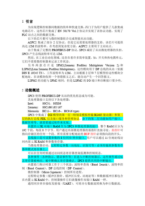
PINOUT
VOUT 1 VCC 2 GND 3 PFI 4
8 VBATT 7 RESET 6 MR 5 PFO
2
© Copyright 2000 Sipex Corporation
元器件交易网
SPECIFICATIONS (continued)
Vcc=4.75V to 5.50V for SP703, VCC = 4.5 0V to 5.50V for SP704, VBATT=2.80V, TA=TMIN to TMAX, typical specified at 25OC, unless otherwise noted.
SP703/704 Low Power Microprocessor Supervisory
1
© Copyright 2000 Sipex Corporation
元器件交易网
ABSOLUTE MAXIMUM RATINGS
These are stress ratings only and functional operation of the device at these ratings or any other above those indicated in the operation sections of the specifications below is not implied. Exposure to absolute maximum rating conditions for extended periods of time may affect reliability and cause permanent damage to the device. VCC........................................................-0.3V to 6.0V VBATT.....................................................-0.3V to 6.0V All Other Inputs......................................-0.3V to (VCC +0.3V) Input Current:
SPC3手册
1 引言为实现逻辑控制器间数据的简单和快速交换,西门子为用户提供了几款集成电路芯片。
这些芯片集成了EN 50170 V o1.2协议并实现了该协议功能,实现了PLC站点之间的数据交换。
以下的芯片都可与微控制器组合完成智能从站功能。
ASPC2集成了部分2层协议,但是它还需要处理器的支持。
该芯片可提供高达12M的波特率。
在考虑到复杂度方面,ASPC2主要用于主站站点。
由于集成了完整的PROFIBUS-DP协议,SPC3减轻了从站微处理器的负担。
SPC3产生总线波特率可达12M。
然而,在工业自动化领域,还存在着许多简单装置,如:开关和热电偶单元,它们不需要微控制器来记录工作状态。
另外两款芯片是SPM2(Siemens Profibus Multiplexer Version 2)和LSPM2(Lean Siemens Profibus Multiplexer)。
这些模块用于DP总线的从站(依据DIN E 19245 T3),工作波特率为12M。
主站根据2层和7层模型给这些模块分配地址。
在该模块收到一个容错报文之后,能自动产生一个回答报文。
LSPM2的功能与SPM2相同,但是LSPM2的I/O端口和诊断接口要少些。
2 功能概述SPC3使得PROFIBUS-DP从站的优化组态成为可能。
其处理器接口支持以下各处理器:Intel: 80C31,80X86Siemens: 80C166/165/167Motorola: HC11-,HC16-,HC916 typesSPC3中集成了OSI模型的第一层(特别是模拟传输RS485驱动器)和第二层的执行总线FDL以及接口服务和管理协议。
余下的第二层功能如用户接口、数据管理等、就需要通过软件来实现。
内置的1.5K双端口RAM作为SPC3和微处理器的接口。
整个RAM区分为192个段,每段8个字节。
用户通过内部微处理器的基指针直接寻址。
基指针可指向存储区的任何一个段。
所有需要分配地址的BUF指针必须指向段的开头。
M1A3P250-2VQ100IVQ100中文资料(Microsemi)中文数据手册「EasyDatasheet - 矽搜」

版本
器件手册章节可以有不同版本号. Actel目标是为客户提供及时事项最新信息.其结果是,该 表数据之前公布 已被充分表征.数据表被指定为"产品简介","高级",并 "生产".这些类别定义如下:
产品简介
产品简介是一个数据表摘要版本(高级或生产),包含 一般产品信息.本文给出具体设备和家庭概况 信息.
I / O说明和使用方法
I/在IGLOO和ProASIC3器件O结构. . . . . . . . . . . . . . . . . . . . . . . . . . . . . . . . . . . . . . . . . . . .7-1 I / O软件控制在低功耗闪存设备. . . . . . . . . . . . . . . . . . . . . . . . . . . . . . . . . . . . . . . . .8-1 DDR为Actel低功耗闪存设备. . . . . . . . . . . . . . . . . . . . . . . . . . . . . . . . . . . . . . . . . . . . . . . .9-1
封装和引脚说明 引脚说明. . . . . . . . . . . . . . . . . . . . . . . . . . . . . . . . . . . . . . . . . . . . . . . . . . . . . . . . . . . . . . . . . . .10-1 包装. . . . . . . . . . . . . . . . . . . . . . . . . . . . . . . . . . . . . . . . . . . . . . . . . . . . . . . . . . . . . . . . . . . . . . .11-1
AP60N03S中文资料

N-CHANNEL ENHANCEMENT MODE POWER MOSFET▼ Low On-Resistance BV DSS 30V ▼ Fast SwitchingR DS(ON)13.5m Ω▼ Simple Drive RequirementI D55ADescriptionAbsolute Maximum RatingsSymbol Units V DS V V GSV I D @T C =25℃A I D @T C =100℃A I DMA P D @T C =25℃W W/℃T STG ℃T J℃Symbol Value Unit Rthj-c Thermal Resistance Junction-case Max. 2.0℃/W Rthj-aThermal Resistance Junction-ambientMax.62℃/WData & specifications subject to change without noticeThermal DataParameterStorage Temperature RangeTotal Power Dissipation 62.5-55 to 150Operating Junction Temperature Range-55 to 150Linear Derating Factor 0.5Continuous Drain Current, V GS @ 10V 35Pulsed Drain Current 1215Gate-Source VoltageContinuous Drain Current, V GS @ 10V 55ParameterRating Drain-Source Voltage 30200218032AP60N03SThe Advanced Power MOSFETs from APEC provide the designer with the best combination of fast switching,ruggedized device design, low on-resistance and cost-effectiveness.The TO-263 package is universally preferred for all commercial-industrial surface mount applications and suited for low voltage applications such as DC/DC converters. The through-hole version (AP60N03P) is available for low-profile applications.± 20G DSTO-263Electrical Characteristics@T j =25o C(unless otherwise specified)Symbol ParameterTest ConditionsMin.Typ.Max.Units BV DSSDrain-Source Breakdown VoltageV GS =0V, I D =250uA 30--V ΔB V DSS /ΔT jBreakdown Voltage Temperature Coefficient Reference to 25℃, I D =1mA-0.037-V/℃R DS(ON)Static Drain-Source On-Resistance V GS =10V, I D =28A -11.513.5m ΩV GS =4.5V, I D =22A -1820m ΩV GS(th)Gate Threshold Voltage V DS =V GS , I D =250uA 1-3V g fs Forward TransconductanceV DS =10V, I D =28A -30-S I DSS Drain-Source Leakage Current (T j =25o C)V DS =30V, V GS =0V --1uA Drain-Source Leakage Current (T j =150o C)V DS =24V, V GS =0V --25uA I GSS Gate-Source Forward Leakage V GS =--nA Q g Total Gate Charge 2I D =28A -22.4-nC Q gs Gate-Source Charge V DS =24V - 2.7-nC Q gd Gate-Drain ("Miller") Charge V GS =5V -14-nC t d(on)Turn-on Delay Time 2V DS =15V -7.4-ns t r Rise TimeI D =28A-81-ns t d(off)Turn-off Delay Time R G =3.3Ω,V GS =10V -24-ns t f Fall Time R D =0.53Ω-18-ns C iss Input Capacitance V GS =0V -950-pF C oss Output CapacitanceV DS =25V -440-pF C rssReverse Transfer Capacitancef=1.0MHz-145-pFSource-Drain DiodeSymbol ParameterTest ConditionsMin.Typ.Max.Units I S Continuous Source Current ( Body Diode )V D =V G =0V , V S =1.3V --55A I SM Pulsed Source Current ( Body Diode )1--215A V SDForward On Voltage 2T j =25℃, I S =55A, V GS =0V--1.3VNotes:1.Pulse width limited by safe operating area.2.Pulse width <300us , duty cycle <2%.AP60N03S± 20V ±100Fig 1. Typical Output Characteristics Fig 2. Typical Output CharacteristicsFig 3. On-Resistance v.s. Gate VoltageFig 4. Normalized On-Resistancev.s. Junction TemperatureFig 5. Maximum Drain Current v.s. Fig 6. Typical Power DissipationCase TemperatureFig 7. Maximum Safe Operating Area Fig 8. Effective Transient Thermal ImpedanceAP60N03SFig 9. Gate Charge Characteristics Fig 10. Typical Capacitance CharacteristicsFig 11. Forward Characteristic ofFig 12. Gate Threshold Voltage v.s.Reverse DiodeJunction TemperatureAP60N03SAP60N03SFig 13. Switching Time Circuit Fig 14. Switching Time WaveformFig 15. Gate Charge Circuit Fig 16. Gate Charge Waveform。
VFS6045型产品特性说明书

VFS6045SA102VFS6045SA151VFS6045SA451VFS6045VA031VFS6045VA102 VFS6045VA121VFS6045VA201VFS6045VA301E M C C o m p o n e n t sNoise suppression filterFor home appliances (conductive noise countermeasure) VFS seriesVFS6045 typeFEATURESAPPLICATIONPART NUMBER CONSTRUCTIONCHARACTERISTICS SPECIFICATION TABLEMeasurement equipmentEquivalent measurement equipment may be used.VFS6045V A031Series nameL×W×H dimensions V: at 10MHzS: at 1MHzInternal codeImpedance6.0×6.0×4.5 mm(Ω)Type Impedance DC resistance Rated current Part No.(Ω)Typ.(Ω)Min.(Ω)typ.(Ω)max.(A)max.6045VA[at 10MHz]57300.0120.0156 6.0VFS6045VA0311451200.0190.0247 5.1VFS6045VA1212422000.0230.0299 4.95VFS6045VA2014683000.0360.0468 3.6VFS6045VA301127510000.0750.0975 2.5VFS6045VA102 6045SA[at 1MHz]1881500.1750.2275 1.5VFS6045SA1515524500.470.6110.9VFS6045SA45112321000 1.15 1.4950.5VFS6045SA102Measurement item Product No.ManufacturerImpedance4294A Keysight T echnologiesDC resistance34420A Hewlett-PackardE M C C o m p o n e n t sVFS6045 typeZ FREQUENCY CHARACTERISTICSINSERTION LOSS VS. FREQUENCY CHARACTERISTICSE M C C o m p o n e n t s VFS6045 typeSHAPE & DIMENSIONSRECOMMENDED LAND PATTERNRECOMMENDED REFLOW PROFILEPACKAGING STYLETEMPERATURE RANGE, INDIVIDUAL WEIGHT *Operating temperature range includes self-temperature rise.**The storage temperature range is for after the assembly.Dimensions in mmDimensions in mmT ype A B KVFS6045 6.3 6.3 4.7Package quantity1500 pcs/reelOperating temperature range*Storagetemperature range**Individualweight–40 to +105 °C–40 to +105 °C0.6 gE M C C o m p o n e n t sREMINDERS FOR USING THESE PRODUCTSBefore using these products, be sure to request the delivery specifications.SAFETY REMINDERSPlease pay sufficient attention to the warnings for safe designing when using this products.The storage period is less than 12 months. Be sure to follow the storage conditions (temperature: 5 to 30°C, humidity: 10 to 75% RH or less).If the storage period elapses, the soldering of the terminal electrodes may deteriorate.Do not use or store in locations where there are conditions such as gas corrosion (salt, acid, alkali, etc.).Before soldering, be sure to preheat components.The preheating temperature should be set so that the temperature difference between the solder temperature and chip temperature does not exceed 150°C.Soldering corrections after mounting should be within the range of the conditions determined in the specifications.If overheated, a short circuit, performance deterioration, or lifespan shortening may occur.When embedding a printed circuit board where a chip is mounted to a set, be sure that residual stress is not given to the chip due to the overall distortion of the printed circuit board and partial distortion such as at screw tightening portions.Self heating (temperature increase) occurs when the power is turned ON, so the tolerance should be sufficient for the set thermal design.Carefully lay out the coil for the circuit board design of the non-magnetic shield type.A malfunction may occur due to magnetic interference.Use a wrist band to discharge static electricity in your body through the grounding wire.Do not expose the products to magnets or magnetic fields.Do not use for a purpose outside of the contents regulated in the delivery specifications.The products listed on this catalog are intended for use in general electronic equipment (AV equipment, telecommunications equip-ment, home appliances, amusement equipment, computer equipment, personal equipment, office equipment, measurement equip-ment, industrial robots) under a normal operation and use condition.The products are not designed or warranted to meet the requirements of the applications listed below, whose performance and/or qual-ity require a more stringent level of safety or reliability, or whose failure, malfunction or trouble could cause serious damage to society,person or property.If you intend to use the products in the applications listed below or if you have special requirements exceeding the range or conditions set forth in the each catalog, please contact us.(1) Aerospace/aviation equipment(2) T ransportation equipment (cars, electric trains, ships, etc.)(3) Medical equipment(4) Power-generation control equipment (5) Atomic energy-related equipment (6) Seabed equipment(7) T ransportation control equipment(8) Public information-processing equipment (9) Military equipment(10) Electric heating apparatus, burning equipment (11) Disaster prevention/crime prevention equipment(12) Safety equipment(13) Other applications that are not considered general-purposeapplicationsWhen designing your equipment even for general-purpose applications, you are kindly requested to take into consideration securing pro-tection circuit/device or providing backup circuits in your equipment.REMINDERSVFS6045SA102VFS6045SA151VFS6045SA451VFS6045VA031VFS6045VA102 VFS6045VA121VFS6045VA201VFS6045VA301。
SP20_Manual_cn说明书

+SP20B/SP20F/SP20X/SP20P编程器使用手册2022-12-20 Revision A6深圳硕飞科技有限公司SHENZHEN SFLY TECHNOLOGY CO.,LTD.目录第一章简介1.1 性能特点 -------------------------------------------------------------------------------------------- 31.2 SP20系列编程器参数表----------------------------------------------------------------------------- 4第二章编程器硬件2.1 编程器主机------------------------------------------------------------------------------------------ 52.2 附件------------------------------------------------------------------------------------------------- 5第三章快速使用3.1 软件安装 -------------------------------------------------------------------------------------------- 63.2 烧录芯片步骤 --------------------------------------------------------------------------------------- 63.3 读取芯片数据并写入新的芯片----------------------------------------------------------------------- 83.4 联机模式指示灯状态 -------------------------------------------------------------------------------- 9第四章脱机烧录4.1下载脱机数据 ---------------------------------------------------------------------------------------104.2 脱机烧录操作----------------------------------------------------------------------------------------11手动方式 -------------------------------------------------------------------------------------------11 自动控制方式(通过ATE接口控制)---------------------------------------------------------------124.3 脱机模式指示灯状态 -------------------------------------------------------------------------------12第五章ISP模式烧录5.1选择ISP烧录模式 ----------------------------------------------------------------------------------135.2 ISP接口定义----------------------------------------------------------------------------------------135.3 连接目标芯片 --------------------------------------------------------------------------------------145.4 选择ISP供电方式----------------------------------------------------------------------------------145.5 烧录操作 -------------------------------------------------------------------------------------------14第六章多机模式烧录6.1 编程器硬件连接 ------------------------------------------------------------------------------------156.2 烧录操作 -------------------------------------------------------------------------------------------16附录一常见问题解答 -------------------------------------------------------------------------------------------- 17附录二免责声明------------------------------------------------------------------------------------------------- 18附录三修订记录-------------------------------------------------------------------------------------------------19第一章简介SP20系列(SP20B/SP20F/SP20X/SP20P)编程器是深圳硕飞科技最新推出的一款SPI FLASH专用高速量产型编程器,是SP16系列的升级版,全面支持国内外各厂商的SPI NOR FLASH、I2C/MicroWire 等EEPROM的高速量产烧录。
爱普生PDG53P0800P5DN电流保护模具说明书

Eaton PDG53P0800P5DNEaton Power Defense molded case circuit breaker, Globally Rated, Frame 5, Three Pole, 800A, 100kA/480V, PXR25 ARMS LSIG w/ Modbus RTU, CAM Link and Relays, No TerminalsEaton Power Defense molded case circuit breakerPDG53P0800P5DN 786679291481139.7 mm 406.4 mm 209.5 mm 21.32 kg Eaton Selling Policy 25-000, one (1) year from the date of installation of theProduct or eighteen (18) months from thedate of shipment of the Product,whichever occurs first.RoHS Compliant IEC 60947-2CCC MarkedUL 489CSAProduct NameCatalog Number UPCProduct Length/Depth Product Height Product Width Product Weight WarrantyCompliancesCertificationsModbus / Relays / CAM100 kAIC at 480 Vac5600800 AThree-pole600 VPD5 Global100 kAIC Icu/ 50 kAIC Ics/ 220 kAIC Icm @380-415V (IEC)85 kAIC Icu/ 40 kAIC Ics/ 187 kAIC Icm @480V Brazil (IEC)200 kAIC @240V (UL)100 kAIC Icu/ 50 kAIC Ics/ 220 kAIC Icm @440V (IEC)100 kAIC @480/277V (UL)35 kAIC Icu/ 18 kAIC Ics/ 73.5 kAIC Icm @690V (IEC)200 kAIC Icu/ 150 kAIC Ics/ 440 kAIC Icm @240V (IEC)40 kAIC Icu/ 25 kAIC Ics/ 84 kAIC Icm @525V South Africa (IEC) 65 kAIC @600/347V (UL)ElectronicClass AComplete breakerNo Terminals600 Vac Eaton Power Defense MCCB PDG53P0800P5DN 3D drawingConsulting application guide - molded case circuit breakersPower Xpert Protection Manager x64Power Xpert Protection Manager x32StrandAble terminals product aidPower Defense brochurePower Defense molded case circuit breaker selection posterPower Defense technical selling bookletPower Defense molded case circuit breakers - Frame 5 product aid Power Xpert Release trip units for Power Defense molded case circuit breakersMolded case circuit breakers catalogPDG5 CSA CertificationPDG5 CB reportEU Declaration of Conformity - Power Defense molded case circuit breakersPDG5 UL authorizationPower Defense Declaration concerning California’s Proposition 65PDG6 CCC certificatePDG6 CSA certificationPDG5 CCC certificationPower Defense Frame 5 walking beam installation instructions -IL012290ENPower Defense Frame 5 key interlock installation instructions -IL012294ENPower Defense Frame 5 breaker status module installation instructions – IL012307ENPower Defense Frame 4_5 flex shaft handle mech assembly instructions - IL012284ENPower Defense Frame 5 interphase barrier kit 3 pole installation instructions - IL012293ENPower Defense Frame 4_5_6 high performance flex shaft handle mechSpecial featuresInterrupt ratingFrameRated operation voltage (Ue) at AC - max Amperage RatingNumber of polesVoltage rating - maxCircuit breaker typeInterrupt rating rangeSwitch off techniqueClassCircuit breaker frame typeTerminalsVoltage rating 3D CAD drawing package Application notesBrochuresCatalogsCertification reports Installation instructionsPXR 25 LSIG w/ARMS Modbus RTU and CAM Link assembly instructions - IL012296ENPower Defense Frame 5 vertical padlockable handle lock hasp installation instructions - IL012283ENPower Defense Frame 2/3/4/5/6 voltage neutral sensor module wiring instructions – IL012316ENPower Defense Frame 5 aux, alarm, shunt trip and uvr instructions(IL012201EN).pdfPower Defense Frame 5 Trip Unit Upgrade Relays Board, Animated Instructions.rhPower Defense Frame 5 Trip Unit Replacement Animated Instructions Power Defense Frame 5 Shunt Trip, Aux and Alarm Trip How-To Video Power Defense Frame 5 Aux, Alarm, ST and UVR Animated Instructions.rh1Power Defense Frame 5 UVR Trip How-To VideoPower Defense Frame 5 Trip Unit Upgrade Wire Harnesses, Animated Instructions.rhPower Defense Frame 6 Trip Unit How-To VideoPower Defense BreakersPower Defense Frame 2 Variable Depth Rotary Handle Mechanism Installation How-To VideoPower Defense molded case circuit breakersPower Defense Frame 5 Trip Unit How-To VideoPower Defense Frame 3 Variable Depth Rotary Handle Mechanism Installation How-To VideoEaton Power Defense for superior arc flash safetyEaton Specification Sheet - PDG53P0800P5DNPower Defense time current curve Frame 5 - PD5Selling Policy 25-000 - Distribution and Control Products and ServicesImplementation of arc flash mitigating solutions at industrial manufacturing facilitiesSingle and double break MCCB performance revisitedMolded case and low-voltage power circuit breaker healthMaking a better machineIntelligent circuit protection yields space savingsTrip TypeCommunicationInstallation videosMultimediaSpecifications and datasheetsTime/current curvesWarranty guidesWhite papersEaton Corporation plc Eaton House30 Pembroke Road Dublin 4, Ireland © 2023 Eaton. All Rights Reserved. Eaton is a registered trademark.All other trademarks areproperty of their respectiveowners./socialmediaIntelligent power starts with accurate, actionable data Safer by design: arc energy reduction techniques Molded case and low-voltage breaker health。
PSS-60-5中文资料

AC/DC Power SupplyFEATURES● 2 Year Warranty● Low Cost, High Reliability● Fixed Switching Frequency● Compact Size, Light Weight● 100% Full Load Burn-In Tested● Cooling by Free Air Convection● Universal AC Input / Full Range● Built-In EMI Filter, Low Ripple and Noise● High Efficiency, Low Working Temperature● Short Circuit, Overload, and Over Voltage ProtectedSPECIFICATIONS: PSS60 SeriesAll specifications are based on 25o C, Nominal Input Voltage, and Maximum Output Current unless otherwise noted.We reserve the right to change specifications based on technological advances.INPUT SPECIFICATIONSInput Voltage Range 85 ~ 264VAC or 120 ~ 370VDCInput Frequency 47 to 63HzAC Current (typical) 2A @ 115VAC 1A @ 230VACInrush Current (typical) Cold Start 20A @ 115VAC 40A @ 230VACLeakage Current < 3.5mA @ 240VACOUTPUT SPECIFICATIONSOutput Voltage See TableOutput Power See TableVoltage Tolerance (See Note 3) PSS-60-5: ±2.0%; Other Models: ±1.0%Voltage Adjustment Range See TableLine Regulation ±0.5%Load Regulation PSS-60-5: ±1.0%; Other Models: ±0.5%Output Current See TableRipple & Noise (max) (See Note 2) PSS-60-5 & PSS-60-12: 120mVp-p; PSS-60-15 & PSS-60-24: 150mVp-pSetup, Rise Time 300ms, 50ms @ 230VAC 800ms, 50ms @ 115VAC and full loadHold Up Time (typical) 80ms @ 230VAC 12ms @115VAC and full loadTemperature Coefficient ±0.03%/°C (0 ~ 50°C)PROTECTIONOver Voltage Protection 115% to 135% (See Table)Protection Type: Hiccup mode, recovers automatically after fault condition is removed.Overload Protection 105 ~ 150% rated output powerProtection Type: Hiccup mode, recovers automatically after fault condition is removed.GENERAL SPECIFICATIONSSwitching Frequency 77KHzEfficiency See TableWithstand Voltage 3000VAC (Input to Output), 1500VAC (Input to FG), 500VAC (Output to FG)Isolation Resistance 100MΩ/500DC (Input to Output, Input to FG, and Output to FG)ENVIRONMENTAL SPECIFICATIONSWorking Temperature -10°C to +60°C (refer to output load derating curve)Storage Temperature -20°C to +85°CWorking Humidity 20 ~ 90% RH non-condensingStorage Humidity 10 ~ 95% RHCooling Free air convectionVibration 10 ~ 500Hz, 2G 10min./1 cycle, 60min each along X, Y, Z axes.MTBF 316,200 hours min. @ 25°C (MIL-HDBK-217F)PHYSICAL SPECIFICATIONSWeight 510 gramsDimensions 159(L) x 97(W) x 38(H) mmWarranty 2 yearsSAFETY & EMCSafety Standards UL1012, UL60950-1, TUV EN60950-1 ApprovedEMI Conduction & Radiation Compliance to EN55022 (CISPR22) Class BHarmonic Current Compliance to EN61000-3-2,-3EMS Immunity Compliance to EN61000-4-2,3,4,5,6,8,11; ENV50204, EN55024, Light industry level, criteria AAC/DC Power SupplyOUTPUT VOLTAGE / CURRENT RATING CHARTModel Number Input VoltageOutput VoltageVoltage Adjust. Range Output CurrentOutput Power Efficiency Over Voltage Protection PSS-60-5 5 VDC 4.75 ~ 5.5V 12A 60W 73% 5.75 ~ 6.75V PSS-60-12 12 VDC 10.8 ~ 13.2V 5A 60W 76% 13.8 ~ 16.2V PSS-60-15 15 VDC 13.5 ~ 16.5V 4A 60W 77% 17.25 ~ 20.25V PSS-60-2485 ~ 264 VAC(120 ~ 370 VDC)24 VDC21.6 ~ 26.4V2.5A60W79%27.6 ~ 32.4VNOTES1. All parameters NOT specially mentioned are measured at 230VAC input, rated load, and 25°C ambient temperature.2. Ripple & noise are measured at 20MHz bandwidth by using a 12" twisted pair-wire terminated with a 0.1uF& 47uF parallel capacitor.3. Tolerances include set up tolerance, line regulation, and load regulation.4. Line Regulation is measured from low line to high line at rated load.5. Load regulation is measured from 0% to 100% rated load.6. The power supply is considered a component, which will be installed into final equipment. The final equipment must be re-confirmed that it still meets EMC directives.BLOCK DIAGRAMDERATING CURVESTATIC CHARACTERISTICS (24V)fosc: 77KHzAC/DC Power SupplyMECHANICAL DRAWINGUnit: mmTerminal Pin No. AssignmentPin No. Assignment1 AC/L2 AC/N3 FG(-V)OUTPUT4 DC(+V)5 DCOUTPUT。
- 1、下载文档前请自行甄别文档内容的完整性,平台不提供额外的编辑、内容补充、找答案等附加服务。
- 2、"仅部分预览"的文档,不可在线预览部分如存在完整性等问题,可反馈申请退款(可完整预览的文档不适用该条件!)。
- 3、如文档侵犯您的权益,请联系客服反馈,我们会尽快为您处理(人工客服工作时间:9:00-18:30)。
Cool MOS™ Power TransistorV DS 600V R DS(on) 1.4ΩI D3.2AFeature• New revolutionary high voltage technology • Ultra low gate charge • Periodic avalanche rated • Extreme d v /d t rated• Ultra low effective capacitances •Improved transconductanceType Package Ordering CodeSPP03N60S5P-TO220-3-1Q67040-S4184SPB03N60S5P-TO263-3-2Q67040-S4197Marking 03N60S503N60S5Maximum Ratings ParameterSymbol Value Unit Continuous drain current T C = 25 °C T C = 100 °CI D3.22APulsed drain current, t p limited by T jmax I D puls 5.7Avalanche energy, single pulse I D = 2.4 A, V DD = 50 VE AS100mJAvalanche energy, repetitive t AR limited by T jmax 1)I D = 3.2 A, V DD = 50 VE AR 0.2Avalanche current, repetitive t AR limited by T jmax I AR 3.2A Gate source voltage V GS ±20V Gate source voltage AC (f >1Hz)V GS ±30Power dissipation, T C = 25°CP tot 38W Operating and storage temperatureT j , T stg-55... +150°CMaximum RatingsParameter Symbol Value Unit Drain Source voltage slopeV DS = 480 V, I D = 3.2 A, T j = 125 °Cd v/d t20V/nsThermal CharacteristicsParameter Symbol Values Unitmin.typ.max. Thermal resistance, junction - case R thJC -- 3.3K/W Thermal resistance, junction - ambient, leaded R thJA--62SMD version, device on PCB: @ min. footprint@ 6 cm2 cooling area 2)R thJA---3562-Soldering temperature,1.6 mm (0.063 in.) from case for 10s3)T sold --260°CElectrical Characteristics, at T j=25°C unless otherwise specifiedParameter Symbol Conditions Values Unitmin.typ.max.Drain-source breakdown voltage V(BR)DSS V GS=0V, I D=0.25mA600--V Drain-Source avalanchebreakdown voltageV(BR)DS V GS=0V, I D=3.2A-700-Gate threshold voltage V GS(th)I D=135µΑ, V GS=V DS 3.5 4.5 5.5Zero gate voltage drain current I DSS V DS=600V, V GS=0V,T j=25°C, T j=150°C --0.5-170µAGate-source leakage current I GSS V GS=20V, V DS=0V--100nA Drain-source on-state resistance R DS(on)V GS=10V, I D=2A,T j=25°C T j=150°C --1.263.41.4-ΩElectrical Characteristics , at T j = 25 °C, unless otherwise specifiedParameter Symbol Conditions Values Unitmin.typ.max. CharacteristicsTransconductance g fs V DS≥2*I D*R DS(on)max,I D=2A- 1.8-SInput capacitance C iss V GS=0V, V DS=25V,f=1MHz -420-pFOutput capacitance C oss-150-Reverse transfer capacitance C rss- 3.6-Turn-on delay time t d(on)V DD=350V, V GS=0/10V,I D=3.2A, R G=20Ω-35nsRise time t r-25-Turn-off delay time t d(off)-40Fall time t f-1522.5Gate Charge CharacteristicsGate to source charge Q gs V DD=350V, I D=3.2A- 3.5-nC Gate to drain charge Q gd-7-Gate charge total Q g V DD=350V, I D=3.2A,V GS=0 to 10V-12.416Gate plateau voltage V(plateau)V DD=350V, I D=3.2A-8-V1Repetitve avalanche causes additional power losses that can be calculated as PAV=E AR*f.2Device on 40mm*40mm*1.5mm epoxy PCB FR4 with 6cm² (one layer, 70 µm thick) copper area for drain connection. PCB is vertical without blown air.3Soldering temperature for TO-263: 220°C, reflowElectrical Characteristics, at T j = 25 °C, unless otherwise specifiedParameter Symbol Conditions Values Unitmin.typ.max. Inverse diode continuousforward currentI S T C=25°C-- 3.2AInverse diode direct current,pulsedI SM-- 5.7 Inverse diode forward voltage V SD V GS=0V, I F=I S-1 1.2VReverse recovery time t rr V R=350V, I F=I S ,d i F/d t=100A/µs -10001700nsReverse recovery charge Q rr- 2.3-µCTypical Transient Thermal CharacteristicsSymbol Value Unit Symbol Value Unittyp.typ.Thermal resistanceR th10.054K/W R th20.103R th30.178R th40.757R th50.682R th60.202Thermal capacitanceC th10.00005232Ws/K C th20.0002034C th30.0002963C th40.0009103C th50.002084C th60.0241 Power dissipation P tot = f (T C)Ptot2 Safe operating areaI D = f ( V DS )parameter : D = 0 , T C=25°C3ID3 Transient thermal impedanceZthJC = f (t p)parameter: D = t p/T10101010K/WZthJC4 Typ. output characteristicI D = f (V DS); T j=25°Cparameter: t p = 10 µs, V GSID5 Drain-source on-state resistance R DS(on) = f (T j)parameter : I= 2 A, V = 10 VRDS(on)6 Typ. transfer characteristicsI D= f (V GS ); V DS≥ 2 x I D x R DS(on)maxparameter: t p = 10 µsID7 Typ. gate chargeV GS= f (Q Gate)parameter: I= 3.2 A pulsedVGS8 Forward characteristics of body diodeI F = f (V SD)parameter: T, t p = 10 µsIF9 Avalanche SOAI AR = f (t AR )par.: T j ≤ 150 °C4I A R10 Avalanche energyE AS = f (T j )par.: I D = 2.4 A, V DD = 50 VE 11 Drain-source breakdown voltage V (BR)DSS= f (T j )SPP03N60S5V (B R )D SS12 Typ. capacitancesC = f (V DS )parameter: V GS =0V,f =1 MHzCDefinition of diodes switching characteristicsP-TO-220-3-1All metal surfaces tin plated, except area of cut. Metal surface min. x=7.25, y=12.3P-TO-263-3-2 (D2-PAK)Published byInfineon Technologies AG,Bereichs KommunikationSt.-Martin-Strasse 53,D-81541 München© Infineon Technologies AG 1999All Rights Reserved.Attention please!The information herein is given to describe certain components and shall not be considered as warranted characteristics.Terms of delivery and rights to technical change reserved.We hereby disclaim any and all warranties, including but not limited to warranties of non-infringement, regarding circuits, descriptions and charts stated herein.Infineon Technologies is an approved CECC manufacturer.InformationFor further information on technology, delivery terms and conditions and prices please contact your nearest Infineon Technologies Office in Germany or our Infineon Technologies Reprensatives worldwide (see address list). WarningsDue to technical requirements components may contain dangerous substances.For information on the types in question please contact your nearest Infineon Technologies Office.Infineon Technologies Components may only be used in life-support devices or systems with the expresswritten approval of Infineon Technologies, if a failure of such components can reasonably be expected tocause the failure of that life-support device or system, or to affect the safety or effectiveness of that deviceor system Life support devices or systems are intended to be implanted in the human body, or to supportand/or maintain and sustain and/or protect human life. If they fail, it is reasonable to assume that the healthof the user or other persons may be endangered.。