This document in subdirectoryRS9949 An Approximation Algorithm for Hypergraph Max k-Cut wit
Molex 34062-000 电子连接器说明书

NOTES: VALID UNLESS OTHERWISE SPECIFIED 1. GENERAL:a. APPLICATION SPECIFICATION SEE: AS-34062-000 -CONTAINS: PRODUCT INTRODUCTION, PRODUCT SUMMARY, CONNECTOR ASSEMBLY, PACKAGING INFORMATION, CONNECTOR MATING, SERVICE INSTRUCTIONS, ELECTRICAL CONTINUITY CHECKING, CRIMPING, AND TROUBLESHOOTING. -DESIGNED TO MATE WITH DEVICE CONNECTION AS SPECIFIED IN DRAWING EWCAP 150-S-002-1-Z01. AVAILIBLE AT /. -DESIGNED TO MATE WITH BLADE SEALED ASSEMBLY AS SPECIFIED IN DRAWING: SD-34675-001 -ASSEMBLY SHIPPED WITH TPA IN PRE-LOCK (SEE TPA PRE-LOCK VIEW IN SHEET 4)b. PRODUCT SPECIFICATION SEE: PS-34062-000 CONTAINS: SCOPE, PRODUCT DESCRIPTION, INTEGRAL COMPONENTS AND ACCESSORIES, APPLICABLE DOCUMENTS AND SPECIFICATIONS, RATINGS, PERFORMANCE, PACKAGING, GAUGE AND FIXTURES, AND OTHER INFORMATION. c. PACKAGING SPECIFICATION PER MOLEX DRAWING: PK-30907-879 d. PARTS MUST BE IN COMPLIANCE TO MOLEX CHEMICAL SUBSTANCES FOR PRODUCTS AND PACKAGING SPECIFICATION: QEHS-699000-301e. DATA MUST BE SUBMITTED UNDER THE MOLEX PART NUMBER TO IMDS (COMPANY ID#13255) 2. DESIGN - MATERIALS:a. SEE BOM TABLE IN SD-34062-004 3. DESIGN - GEOMETRY:a. THIS IS A 100% CAD GENERATED PART. THE CAD MATHEMATICAL DATA IS THE MASTER FOR THIS PART. FOR DIMENSIONAL OR ANY INFORMATION NOT SHOWN ON THIS DRAWING, ANALYZE THE CAD MODEL.b. GEOMETRIC DIMENSIONS AND TOLERANCES PER ASME Y14.5M - 1994c. EDGES AND UNDIMENSIONED DETAILS PER ISO13715d. CORNERS SHOWN AS SHARP TO BE R 0.2 MAX.e. LETTERING SHALL BE 0.15 MAX RAISED IN 0.25 MAX RECESS PAD.THIS INCLUDES RECYCLING CODE, CAVITY ID, VENDOR IDENTIFICATION,AND CUSTOMER MATERIAL NUMBER.f. VISUAL DEFECTS SHALL MEET COSMETIC STANDARD PS-45499-002 (Class B)g. LASER MARKING: TBD TABLE OF CONTENTS SHEET NO.SHEET DESCRIPTION1NOTES 2, 3CONFIGURATIONS 4RECEPTACLE CONNECTOR ASSEMBLY 5MOLEX INTERFACEJ19NX RE-MASTERING J18ADDED DIM ICD 64REV.DESCRIPTION INSPECTION BALLOON NUMBER LOG GENERAL TOLERANCES (UNLESS SPECIFIED)ANGULAR TOL ± 3.0°4 PLACES±3 PLACES±THIS DRAWING CONTAINS INFORMATION THAT IS PROPRIETARY TO MOLEX ELECTRONIC TECHNOLOGIES, LLC AND SHOULD NOT BE USED WITHOUT WRITTEN PERMISSION DIMENSION UNITS SCALE MM 4:1DRWN BY DATE KCUNNINGHAM 2011/11/08CHK'D BY DATE MX150 2 WAY CABLE SEAL RECEPTACLE CONN. SYSTEM (5.0MM PITCH)2017/05/152017/06/14QUALITY SYMBOLS =0=0=0CPA OPTIONAL SEE BOM CONNECTOR HOUSING FOR OPTIONS SEE BOM RING SEAL FOR OPTIONS SEE BOM TPA B B C CD DE EF FG GHH JJ K K L LSHEET DESCRIPTIONCONFIGURATIONS OPTION B OPTION COPTION EOPTION F2.255.504X 1.50R 3.0±1.0R OPTION A OPTION DGENERAL TOLERANCES (UNLESS SPECIFIED)ANGULAR TOL ± 3.0°4 PLACES ±3 PLACES±THIS DRAWING CONTAINS INFORMATION THAT IS PROPRIETARY TO MOLEX ELECTRONIC TECHNOLOGIES, LLC AND SHOULD NOT BE USED WITHOUT WRITTEN PERMISSION DIMENSION UNITS SCALE MM 2:1DRWN BY DATE KCUNNINGHAM 2011/11/08CHK'D BY DATE MX150 2 WAY CABLE SEAL RECEPTACLE CONN. SYSTEM (5.0MM PITCH)2017/05/152017/06/14QUALITY SYMBOLS =0=0=05.504X 1.50R NON CLIP-SLOT OPTIONSCALE 4:1MINIMUM PASS-THRU WITH NO CLEARANCE APPLIES TO NON-CLIP SLOT OPTIONS A, C, D & G23.40⌀MINIMUM PASS-THRU WITH NO CLEARANCE APPLIES TO NON-CLIP SLOT OPTIONS B, E & F26.00⌀6.50REAR VIEWREAR VIEWB BC CD DE EF FG GHH J JK KL LGENERAL TOLERANCES (UNLESS SPECIFIED)ANGULAR TOL ± 3.0°4 PLACES ±3 PLACES±THIS DRAWING CONTAINS INFORMATION THAT IS PROPRIETARY TO MOLEX ELECTRONIC TECHNOLOGIES, LLC AND SHOULD NOT BE USED WITHOUT WRITTEN PERMISSION DIMENSION UNITS SCALE MM 2:1DRWN BY DATE KCUNNINGHAM 2011/11/08CHK'D BY DATE MX150 2 WAY CABLE SEAL RECEPTACLE CONN. SYSTEM (5.0MM PITCH)2017/05/152017/06/14QUALITY SYMBOLS =0=0=0SHEET DESCRIPTIONCONFIGURATIONS MINIMUM PASS-THRU WITH NO CLEARANCE APPLIES TO CLIP-SLOT OPTIONS A, C & D25.50⌀MINIMUM PASS-THRU WITH NO CLEARANCE APPLIES TO CLIP-SLOT OPTION B 26.00⌀OPTION B W/CLIP-SLOT *OPTION C W/CLIP-SLOT ** WITH CLIP-SLOT CONFIGURATIONSDO NOT MEET USCAR PACKAGING FRAME REQUIREMENTSCLIP-SLOT OPTION SCALE 4:1OPTION A W/CLIP-SLOT *6.50 2.255.503.0±1.0R 4X 1.50R 5.504X 1.50R OPTION D W/CLIP-SLOT *B B C CD DE EF FG GH HJ JK KL LGENERAL TOLERANCES (UNLESS SPECIFIED)ANGULAR TOL ± 3.0°4 PLACES ±3 PLACES ±THIS DRAWING CONTAINS INFORMATION THAT IS PROPRIETARY TO MOLEX ELECTRONIC TECHNOLOGIES, LLC AND SHOULD NOT BE USED WITHOUT WRITTEN PERMISSION DIMENSION UNITS SCALE MM 4:1DRWN BY DATE KCUNNINGHAM 2011/11/08CHK'D BY DATE MX150 2 WAY CABLE SEAL RECEPTACLE CONN. SYSTEM (5.0MM PITCH)2017/05/152017/06/14QUALITY SYMBOLS =0=0=0SHEET DESCRIPTIONRECEPTACLE CONNECTOR ASSEMBLY OPTIONAL LASER MARKING SURFACESEE NOTE 3g 3.3532.230.85±0.20HOUSING MOLD CAVITY CODE RECYCLE CODE TERMINAL CAVITY ID.MANUFACTURINGLOCATION CODETERMINAL CAVITY IDCHARTED DIMENSIONS CONFIGURATIONS DIMENSIONS A B OPTIONS A, C, D16.622.0OPTION B16.623.9OPTION E20.223.9OPTION F16.623.9OPTION G18.422.0OPTIONS A, C, D W/CLIP-SLOT19.222.0OPTION B W/CLIP-SLOT19.223.9OPTIONAL LASER MARKING SURFACESEE NOTE 3gSECTION B -B B B TPA SHOWN IN5.00 2.50DIM A MAX.DIM B MAX.AA31.30B B C CD DE EF FG GH HJJ K KL LMX150 2 WAY CABLE SEAL RECEPTACLE CONNECTION SYSTEM (5.0mm PITCH)BOM AND PIN OUT SHEET ABBREVIATION COLOR MATERIAL A-BLK BLACK PA6 GF30B-LG LIGHT GRAY PA6 GF30B-BLK BLACK PA6 GF30C-BLKBLACK PA6 GF30D-BLKBLACK PA6 GF30D-LGLIGHT GRAY PA6 GF30E-BLKBLACK PA6 GF30F-LGLIGHT GRAY PA6 GF30G-BLKBLACK PA6 GF30A-BLK-CLIPBLACK PA6 GF30B-LG-CLIPLIGHT GRAY PA6 GF30B-BLK-CLIPBLACK PA6 GF30C-BLK-CLIPBLACK PA6 GF30D-BLK-CLIPBLACK PA6 GF30D-LG-CLIPLIGHT GRAY PA6 GF30A-BLK-SVBLACK PA6 GF30C-BLK-SVBLACK PA6 GF30D-BLK-SVBLACK PA6 GF30R3MEDIUM BLUE INHERENTLY LUBRICATED SILICONE R4GREEN INHERENTLY LUBRICATED SILICONE CPARED PBT GF30TPA NATURAL PBT GF30FOR ADDITIONAL INFORMATION SEE SD-34062-002HOUSING OPTION/COLOR TPA CPA RING SEAL OPTION A, BLACK, W/O CPA34062-0021A-BLK TPA R3-40°C TO 125°C 12SALEABLE OPTION B, LIGHT GRAY, W/O CPA34062-0022B-LG TPA R3-40°C TO 125°C 123SALEABLE PREFERRED, FULLY SHROUDED OPTION C, BLACK, W/O CPA34062-0023C-BLK TPA R3-40°C TO 125°C 123SALEABLE PREFERRED, FULLY SHROUDED OPTION D, BLACK, W/O CPA34062-0024D-BLK TPA R3-40°C TO 125°C 12SALEABLE OPTION D, LIGHT GRAY, W/O CPA34062-0029D-LG TPA R3-40°C TO 125°C 12SALEABLE OPTION A, BLACK, W/ CPA34062-0025A-BLK TPA CPA R3-40°C TO 125°C 12SALEABLE OPTION B, LIGHT GRAY, W/ CPA34062-0026B-LG TPA CPA R3-40°C TO 125°C 123SALEABLE PREFERRED, FULLY SHROUDED OPTION C, BLACK, W/ CPA34062-0027C-BLK TPA CPA R3-40°C TO 125°C 123SALEABLE PREFERRED, FULLY SHROUDED OPTION D, BLACK, W/ CPA34062-0028D-BLK TPA CPA R3-40°C TO 125°C 12SALEABLE OPTION D, LIGHT GRAY, W/ CPA34062-0030D-LG TPA CPA R3-40°C TO 125°C 12SALEABLE OPTION A, BLACK, WITH CLIPSLOT, W/O CPA34062-0031A-BLK-CLIP TPA R3-40°C TO 125°C 12SALEABLE OPTION B, LIGHT GRAY, WITH CLIPSLOT, W/O CPA34062-0032B-LG-CLIP TPA R3-40°C TO 125°C 123SALEABLE PREFERRED, FULLY SHROUDED OPTION C, BLACK, WITH CLIPSLOT, W/O CPA34062-0033C-BLK-CLIP TPA R3-40°C TO 125°C 123SALEABLE PREFERRED, FULLY SHROUDED OPTION D, BLACK, WITH CLIPSLOT, W/O CPA34062-0034D-BLK-CLIP TPA R3-40°C TO 125°C 12SALEABLE OPTION D, LIGHT GRAY, WITH CLIPSLOT, W/O CPA34062-0035D-LG-CLIP TPA R3-40°C TO 125°C 12SALEABLE OPTION A, BLACK, WITH CLIPSLOT, W/ CPA34062-0036A-BLK-CLIP TPA CPA R3-40°C TO 125°C 12SALEABLE OPTION B, LIGHT GRAY, WITH CLIPSLOT, W/ CPA34062-0037B-LG-CLIP TPA CPA R3-40°C TO 125°C 123SALEABLE PREFERRED, FULLY SHROUDED OPTION C, BLACK, WITH CLIPSLOT, W/ CPA34062-0038C-BLK-CLIP TPA CPA R3-40°C TO 125°C 123SALEABLE PREFERRED, FULLY SHROUDED OPTION D, BLACK, WITH CLIPSLOT, W/ CPA34062-0039D-BLK-CLIP TPA CPA R3-40°C TO 125°C 12SALEABLE OPTION D, LIGHT GRAY, WITH CLIPSLOT, W/ CPA34062-0040D-LG-CLIP TPA CPA R3-40°C TO 125°C 12SALEABLE OPTION A, BLACK, SEVERE VIBRATION, W/ CPA34062-4006A-BLK-SV TPA CPA R4-40°C TO 155°C 12SALEABLE OPTION C, BLACK, SEVERE VIBRATION, W/ CPA34062-4008C-BLK-SV TPA CPA R4-40°C TO 155°C 12SALEABLE PREFERRED, FULLY SHROUDED OPTION D, BLACK, SEVERE VIBRATION, W/ CPA34062-4009D-BLK-SV TPA CPA R4-40°C TO 155°C 12SALEABLE OPTION E, BLACK, W/O CPA34062-0041E-BLK TPA R4-40°C TO 155°C 2SALEABLE PREFERRED, FULLY SHROUDED OPTION F, LIGHT GRAY, W/O CPA34062-0042F-LG TPA R4-40°C TO 155°C 2SALEABLE PREFERRED, FULLY SHROUDED OPTION G, BLACK, W/O CPA34062-0043G-BLK TPA R4-40°C TO 155°C 2SALEABLE PREFERRED, FULLY SHROUDED OPTION E, BLACK, W/ CPA34062-0044E-BLK TPA CPA R4-40°C TO 155°C 2SALEABLE PREFERRED, FULLY SHROUDED OPTION F, LIGHT GRAY, W/ CPA34062-0045F-LG TPA CPA R4-40°C TO 155°C 2SALEABLE PREFERRED, FULLY SHROUDED OPTION G, BLACK, W/ CPA34062-0046G-BLK TPA CPA R4-40°C TO 155°C 2SALEABLE PREFERRED, FULLY SHROUDED OPTION A, BLACK, W/ CPA34062-0047A-BLK TPA CPA R3-40°C TO 125°C 12SALEABLE OPTION B, LIGHT GRAY, W/O CPA34062-0048B-LG TPA R4-40°C TO 155°C 123SALEABLE PREFERRED, FULLY SHROUDED OPTION C, BLACK, W/O CPA34062-0049C-BLK TPA R4-40°C TO 155°C 123SALEABLE PREFERRED, FULLY SHROUDED OPTION B, LIGHT GRAY, W/ CPA34062-0050B-LG TPA CPA R4-40°C TO 155°C 123SALEABLE PREFERRED, FULLY SHROUDED OPTION C, BLACK, W/ CPA34062-0051C-BLK TPA CPA R4-40°C TO 155°C 123SALEABLE PREFERRED, FULLY SHROUDED OPTION B, LIGHT GRAY, WITH CLIPSLOT, W/O CPA34062-0052B-LG-CLIP TPA R4-40°C TO 155°C 123SALEABLE PREFERRED, FULLY SHROUDED OPTION C, BLACK, WITH CLIPSLOT, W/O CPA34062-0053C-BLK-CLIP TPA R4-40°C TO 155°C 123SALEABLE PREFERRED, FULLY SHROUDED OPTION B, LIGHT GRAY, WITH CLIPSLOT, W/ CPA34062-0054B-LG-CLIP TPA CPA R4-40°C TO 155°C 123SALEABLE PREFERRED, FULLY SHROUDED OPTION C, BLACK, WITH CLIPSLOT, W/ CPA34062-0055C-BLK-CLIP TPA CPA R4-40°C TO 155°C 123SALEABLE PREFERRED, FULLY SHROUDED OPTION C, BLACK, SEVERE VIBRATION, W/O CPA34062-4003C-BLK-SV TPA R4-40°C TO 155°C 12SALEABLE PREFERRED, FULLY SHROUDED OPTION D, BLACK, SEVERE VIBRATION, W/O CPA34062-4004D-BLK-SV TPA R4-40°C TO 155°C 12SALEABLE OPTION D, BLACK, WITH CLIPSLOT, W/ CPA34062-0056D-BLK-CLIP TPA CPA R4-40°C TO 155°C 12SALEABLE OPTION A, BLACK, WITH CLIPSLOT, W/ CPA34062-0057A-BLK-CLIP TPA CPA R3-40°C TO 125°C 12SALEABLE OPTION B, BLACK, W/O CPA34062-0058B-BLK TPA R3-40°C TO 125°C 123SALEABLE PREFERRED, FULLY SHROUDED OPTION B, BLACK, W/ CPA34062-0059B-BLK TPA CPA R3-40°C TO 125°C 123SALEABLE PREFERRED, FULLY SHROUDED OPTION B, BLACK, WITH CLIPSLOT, W/O CPA34062-0060B-BLK-CLIP TPA R3-40°C TO 125°C 123SALEABLE PREFERRED, FULLY SHROUDED OPTION B, BLACK, WITH CLIPSLOT, W/ CPA 34062-0061B-BLK-CLIP TPA CPA R3-40°C TO 125°C 123SALEABLE PREFERRED, FULLY SHROUDEDCOMMENTS INSERT, TPA 13HOUSING OPTION C - SEVERE VIBRATION HOUSING OPTION D - SEVERE VIBRATION RING SEAL TEMP. CLASS 3RING SEAL TEMP. CLASS 4CPA 2RECOMMENDED MATING DEVICEPRODUCTION TOOL STATUS ASSEMBLY DESCRIPTION ASSEMBLY PART NUMBERCOMPONENTTHE PRESENCE OF AN ABBREVIATION INDICATES THE PRESENCE OF THAT COMPONENT.ASSEMBLY OPERATING TEMPERATURE HOUSING OPTION D WITH CLIPSLOT E-34675-001MOLEX INLINE MALE CONNECTOR 3HOUSING OPTION C WITH CLIPSLOT HOUSING OPTION F HOUSING OPTION G HOUSING OPTION A WITH CLIPSLOT HOUSING OPTION B WITH CLIPSLOT cart 150-S-002-1-Z01HOUSING OPTION B 2MOLEX INTERFACE SD-34062-002SHEET 5HOUSING OPTION D HOUSING OPTION E HOUSING OPTION A - SEVERE VIBRATION HOUSING OPTION B WITH CLIPSLOT BOM/ APPLICABLE COMPONENTS TABLE HOUSING OPTION D WITH CLIPSLOT RECOMMENDED MATING DEVICE TABLEDESCRIPTION HOUSING OPTION A HOUSING OPTION B ABBREVIATION DESCRIPTION DRAWINGINFORMATION ADDITIONAL INFORMATIONUSCAR INTERFACE 1HOUSING OPTION C HOUSING OPTION D ECN NO.: 614442DATE:2019/3/26DOCUMENT NO.: SD-34062-004REVISION: A3PAGE: 1 OF 1。
Brother PT-9500PC 打印机 Linux 驱动程序说明书

Appendix A Printer properties..........................................................................................................................9
This software provides the installer package that automatically copies the appropriate driver file (from those mentioned above) to your Linux distribution.
Table of Contents
1. Overview 1
1.1.
Introduction ..................................................................................................................................1
F.1. Retrieving print error information...............................................................................................23
F.2. MFC-compatible Linux drivers...................................................................................................23
NUVOTON NuCam 硬件用户手册说明书

NNuvot The info Nuvoton Tech ton is providinFor addition Nu Hard formation desc hnology Corpo ng this docum design. Nuvo All data andnal informatio N329uMak dwar cribed in this oration and sh ment only for r oton assumes d specification on or questionw AR 905 F ker Nu re Use document is hall not be repreference purp s no responsib ns are subjecns, please con www.nuvoton.cRM ® AR 32-b amily uWica er Ma the exclusive produced with poses of NuM bility for error ct to change w ntact: Nuvoto comRM926E it Micro yam anuale intellectual p hout permissio Micro microcon rs or omission without noticen Technology EJ-S B oproce property ofon from Nuvo ntroller based ns..y Corporationasedessoroton.d system.Table11.122.12.22.32.42.52.62.62.62.62.72.82.82.82.82.92.1033.13.23.33.43.5456e of ConOVERVIEWNuWicaIntroductioNuWicaN32905GC030TVP515RTL818Board I6.1 NuWi6.2 NuWi6.3 NuWiNuWicaNuWica8.1 NuWi8.2 NuWi8.3 NuWiN32905NuWicaNuWiCamNuWicaNuWicaNuWicaNuWicaNuWicaStarting toExample CREVISIONntentsW..........am Systemon to NuWiam Key Fea5R3DN on N8 on NuWic50/GM715089FTV on NIntroductioncam-VGA Bocam-TVP Bocam-Debugam Power Sam Jumpercam-VGA Bocam-TVP Bocam-Debug5R3DN Pinam PCB PlaSchematicam-VGA Scam-VGA Scam-TVP Scam-TVP Scam-Debug SUse NuWCode.......N HISTORY............Block ......cam.......atures ......NuWicam Fcam Feature0 on NuWicaNuWicam Fen .............oard ..........oard ..........Board........Scheme ....and Conneoard Jumperoard JumperBoard JumpeAssignmenacement ...cs .........chematic (1/chematic (2/hematic (1/2hematic (2/2Schematic (WiCam .................Y.................................................................Features ....es ...........am Featureeatures .................................................................................ector .........r Description.Description.er Descriptiont for Conne.........................../2) .........../2) ...........2) ...........2) ...........(1/1)................................................................................................................................s....................................................................................................................................................on .............ectivity .................................................................................................................................................................................................................................................................................................................................................................................................................................................................................................................................................................................................................................................................................................................................................................................................................................................................................................................................................................................................................................................................................................................................................................................................................................................................................................................................................. (3) (3) (4) (4) (5) (6) (7) (8) (9).. 10.. 11.. 12.. 12.. 13.. 13.. 15.. 17.. 18.. 21. 24.. 24.. 25.. 26.. 27.. 28. 29. 30. 311 O Nu vidTh de funTh rem theTh TX de exN 1.1Figex OVERVIEW uvoton’s NuM deo and audi he NuWicam ecoder, voice nctions make he NuWicam motely. The e Wi-Fi came he NuWicam XD/RXD prot evice and Ar xpand various NuWicam S gure 1-1 shoxternal device WMaker NuWic io data to a w integrates n e microphon e a cost effec can be use NuWicam p era easily and m has an ext ocol of UART rduino microc s possible ap System Bl ows the NuWes. Key part f cam is an op wireless rece necessary fu ne, SDIO ho ctive solution ed for home rovides an A d connect to ternal conne T for commu controller or pplications. ockWicam syste features in NFigure 1-1pen source hiver through unctions such ost controlle for Wi-Fi ca security or m App supports it from every ector that pro unication, suc for Nuvoton em architect NuWicam are NuWicam Sardware devWi-Fi.h as CMOS er for conne mera applica monitoring th s iOS and An ywhere throu ovides Ardui ch as do som n’s NuEdu-SD ture and per also listed.System Block vice supports sensor or T ecting with W ations. he elders, ba ndroid that a gh a smartph no microcon me data sam DK- M451 d ripheral interks P2P that traTV video (NT Wi-Fi moduleabies or pets allows users hone or table ntroller based mpling betwee development rfaces for coansmits aTSC/PAL) e. Theseat hometo set up et.d kit withen mobileboard to onnecting2 INThN3SDCMdifsptwmiN2.1●●●●●●●●●●●●●●NTRODUChe NuWicam32905R3DNDIO Wi-Fi mMOS sensorfferential micpeed device pwo UART poicrocontrollerNuWicamSOC: N3Main proVGA CMAlternativVideo strSDIO WiEmbeddeSupports3 LEDs foWide powSystem oMain PCBDebug to⏹ Softport⏹ MesPower co⏹ A/V⏹ WorTION TO Nm uses anprovides themodule for wor TV videocrophone intport to PC foorts, port 0r based kit coFeatures32905R3DN (gram with 8OS Image Sve video withreaming achi-Fi module wed Electret Cs Arduino micor status indiwer supply inoperation in LB size: 25mmooling board,tware develotssage debugonsumptionstreaming rurking time ofNUWICAMARM926 Se SPI interfaireless netwoo (NTSC/PAterface withr software deis dedicateommunication(ARM926 atMB SPI Flasensor (GC03h TV video deeves MJPGwith RTL8189Condenser Mcrocontrollerication, Prognput range froLinux OS 3.4m x 50mmwhich is useopment or SPging with UAunning up to6 hours is poMOC whichce for SPI Nork connectiL) decoder fECM type fevelopment oed for debun.192 MHz, 32sh (W25Q64F308)ecoder, TVP5performance9FTV,softwaricrophonecommunicatiram Ready, Wom 3.5V to 6V4.35ed for:PI flash progrART port 0 th200mA at 5Vossible with 1N32905R3DNOR flash boion, providesfor Motion JPfor audio stror SPI flash’sugging and2 MB DDR2 wFV, SO8)5150/ GM715e at VGA@30re AP mode sion based onWi-Fi Link &Vram updatedrough USB vV (typical)1500mAH AADN as the Sooting, provids a video inPEG video sreaming, pros program upthe UARTwith TQFP6450 (NTSC/PA0fpssupport andn TXD/RXD pApp runningby the utilityvirtual COMA BAT x 4SOC microcdes a SD intput interfacestreaming, provides an USpgrade. It alsport 1 for4 package)AL support)easy to confprotocolgof PC througcontroller,terface toe to VGArovides aSB2.0 Hio provideArduinoiguregh USBN 2.2●● ● ● ● ●● ● ● ● ●PlN32905R3D N32905R CPU ope SRAM@System bCCIR601Resolutio video stre DMA acc 10-bit Au USB2.0 H Two UAR Package ease refer to DN on NuW R3DN: Nuvot erated at 1928K and Inter booting with S 1 & CCIR656on up to 2M p eaming celerate that udio ADC with Hi speed, driv RT ports supp , TQFP-64 (Mo Figure 2-1 f Wicam Fea ton’s ARM9 f MHz,1.8V w rnal Booting R SPI NOR flas 6 interfaces fo pixel for Still SD data tran h Microphone ver support M port debuggi MCP, stacke for the N3290Figure 2-1 N aturesfamily based with 8KB I-Ca ROM, IBR@sh or CMOS ima Image Captu nsfer with SD e pre-Amp &MS (Mass St ng and Ardu d with 32MB 05R3DN SON32905R3DN on the ARM ache & 8KB D 16Kage sensor ure, 640x480IO Wi-Fi mod & AGC torage) Class ino controller **********C outline.N SOC Outlin 926EJ-S cor D-Cache 0 (VGA) resol dule s r communica V)nere lution for MJPationPEGG2.3●●●●●●●PlGC0308 onGC0308:ResolutioOn-ChipOperatingOutput foSingle poSupport Hease refer ton NuWicam: GalaxyCoreon 640V x 48ISP providesg at up to 30ormats: YCbCower supply (Horizontal /Vo Figure 2-2 fFigurem Featurese’s CMOS im80H with 1/6.5s AE (Auto Eframes per sCr4:2:2(3V)Vertical mirrorfor the GC03e 2-2 GC030smage sensor5-inch opticaExposure) andsecond at 24r control308 CMOS se08 CMOS Seal formatd AWB (Auto4 MHz clock iensor modulensor Moduleo White Balanin VGA modee outline.e Outlinence) controleT 2.4●● ● ● ● ● ● ●● ●PlTVP5150/G TVP5150GM7150 Both vide Support N The outp Single 14Support p NTSC/PA ⏹ TVP ⏹ GM TVP5150GM7150 ease refer toGM7150 on 0: Ti’s NTSC/is Chengdu eo decoders NTSC (N, 4.4put formats ca 4.318-MHz C power-on res AL detection P5150 can su M7150, detect 0 PKG is LQF PKG is QFN o Figure 2-3 f Figure 2n NuWicam/PAL video d GoldTel (成都are pin out c 43), PAL (B, an be 8-bit 4:Crystal for all set upport auto d tion by jumpe FP32 N32for the TVP52-3 TVP5150/m Featuresdecoder 都国腾) NTSC compatible D, G, H, I, M :2:2 or 8-bit Istandards detectioner setting150/ GM715/ GM7150 TV C/PAL video M, N) Video d TU −R BT.6550 TV video dV video deco decoderata source56 decoder outlin oder outlinene.R2.5●●●●●●●PlRTL8189FTRTL8189OperateModulesOperateSecurity1T(transand 150NuWicamease refer toTV on NuW9FTV: Realted at 802.11nsize is 12.0 mat ISM 2.4Gcan apply Wsmitter) andMbps upstrem Network Ao Figure 2-94FigureWicam Feaek’s Wi-Fi chn Wi-Fi LGA Mmm x12.0 mmGHz frequencWPA/WPA2 c1R (receiveream PHY ratArchitecture w4 for the RTL82-4 RTL818turesipModulem x 1.6mm, 3cy bandscertification fo) allow data resworking at so8189FTV SD89FTV SDIO3.3V at SDIOor Wi-Fi.rates supportftware AP mDIO Wi-Fi moWi-Fi ModuleO Interfaceting up to 15odeodule outlinee Outline0 Mbps down nstreamB 2.6As shodebug●● ●Board Intro own in Figure board, as de NuWicam NuWicamNuWicam oductione 2-5, the NuW escribed belo m-VGA: Wi-F m-TVP: Wi-F m-Debug:De Wicam soluti ow: Fi camera ma Fi camera ma ebug boardFigure 2-5on contains t ain board witain board with5 NuWicam P two kinds of th VGA CMOh TV video dPCB Outlinemain boardsOS sensorecoders and one commmon2.6.1The NubasedstreamresolutNuWicam-uWicam-VGAon Nuvoton’sming over Wi-tion.-VGA BoardA board usess N32905R3Fi network wFigure 2-6ds GC0308 VGDN for encodwith RTSP seNuWicam-VGGA CMOS seding. NuWicarver. The forGA Board (Fensor and proam firmwaremat of videoFront View anovides a powprovides botstream is Mond Rear Viewwerful JPEG cth audio andotion-JPEG ww)codecvideowith VGA2.6.2 The Nu analog encodi server.NuWicam-uWicam-TVP camera and ng. NuWicam The format -TVP Board P board uses d based on N m firmware pof video streFigure 2-7dTVP5150 or uvoton’s N32rovides botham is Motion NuWicam-TV r GM7150 TV 2905R3DN toaudio and vn-JPEG withVP Board (FV video decod o provide a pideo streami VGA resolut ront View an der for conne powerful JPE ng over Wi-F ion. nd Rear View ecting NTSC EG codec for Fi network wit w)C or PALvideo th RTSP2.6.3The Nusoftwarfrom thN2.7Figurerequireboard dNuWicam-uWicam-Debre developmehe N32905R3NuWicam2-9 shows thement to provdamaged or-Debug Boabug board is cent or SPI fla3DN UART pFigure 2-8 NPower Schhe NuWicamvide that corrbroken.ardconnected toash’s programport 0 throughNuWicam-Dehemesystem powrect power voFigure 2-9o the NuWicam upgrade. Uh USB Virtuaebug Board (Fwer scheme, uoltage to NuWNuWicam Poam-VGA or NUser can alsoal COM.Front View auser should fWicam to preower SchemeuWicam-TVPo get the debnd Rear Viewfollow the poevent incorreceP main boardbugging messw)ower distributct voltage cad forsageionusedN2.82.8.1FigureNuWicam JNuWicam-2-10 showsFigure 2-10 N●CONmicr⏹Note:Fi camUSBprefe⏹Jumper an-VGA Boardthe front andNuWicam-VGN1: This connrocontroller bCON1. pin◆ PIN1◆ PIN2: The pin 1-2mera functionpower, abour and recommCON1. Pincommunicand Connecd Jumper Dd rear view ofGA Board & Nnector is an ebased kit1-2, it is for p, input voltag2, connect it t2 of CON1 isn with an indt voltage reqmended.3 & 4, UARTationVSS3.5V~6V,VIN Q2SDGctorDescriptionf NuWicam-VNuWicam-Deexpanded copower supplyge range fromto GNDconnected toependent poquest is fromT protocol ofHTXDHRXD, BAT/DC-SI2301CDSVGA Board &ebug Board (onnector for cy or BAT conm +3.5V to +6o power suppower supply w3.5V (Min.) tinterface wit& NuWicam-D(Front View aconnecting tonnection6Vply or BAT, Nwithout NuWito 6V (max.),th TXD/RXDDebug Boardand Rear Vieo ArduinoNuWicam canicam debug btypical DC 5for Arduinod.ew)n run Wi-board’s5V is● CON● SW1⏹N2: This conn1: RESET KESystem re-nector is forEY-start when thconnecting whe button is pwith NuWicampressedm-Debug boaard’s CON32.8.2Figure NuWicam-2-11 showsFigure 2-11●J1: ●J2: ⏹ ⏹Note jump ●CON kit⏹ Note:Fi cam USB prefe ⏹-TVP Board the front view NuWicam-TV NTSC/ PAL NTSC/ PAL v Jumper J2 Jumper J2 e: TVP5150 per J2 setting N1: This is an CON1. pin ◆ PIN 1◆ PIN 2: The pin 1-2mera function power, abou r and recomm CON1. Pin communicad Jumper De w and rear vi VP Board & N analog came video source open expresclose exprescan automat g. n expanded 1-2, is for po: input voltag 2: connect it t 2 of CON1 is n with an ind t voltage req mended. 3 & 4, UART ation escriptioniew of NuWic NuWicam-Deera input con e selection (th sses video so sses Video s tically identify connector fo ower supply o ge range from to GNDconnected to ependent po quest is from T protocol of cam-TVP Boa ebug Board (nector his jumper fu ource is NTS ource is PAL y NTSC/PAL r connecting or BAT conne m +3.5V to +o power supp ower supply w 3.5V (Min.) t interface wit ard & NuWic (Front View a unction only f C L L signals by fi to Arduino m ection 6V ply or BAT, N without NuWi to 6V (max.),th TXD/RXD cam-Debug B and Rear Vie for GM7150 u irmware itsel microcontrolle NuWicam can icam debug b typical DC 5for ArduinoBoard.ew)use)f without er based n run Wi-board’s 5V is●CON●SW1⏹N2: This con1: RESET KESystem re-nector is forEY-starts when tconnecting wthe button iswith NuWicampressed.m-Debug boa ard’s CON32.8.3 FigureNuWicam-2-12 shows ● J1: U ⏹ ⏹Note: For Guide.pdf● CON ⏹ ● CON ⏹ ● CON⏹N ote: ForNuWicam -Debug Boa the front viewFigure 2-1USB recover J1 jumper o J1 jumper c Flash progr r AutoWriter f”.N2: USB con Used for Umust conneN3:Connected.N4: VCOM co User can gUSB Virtuar Virtual COMm User Guide ard Jumper w and rear vi 12 NuWicam ry mode sele open, for nor close, N3290ram upgrade program ope nnectorSB applicatio ect USB cabl to NuWicam onnector et that debug al COMM driver insta e.pdf”.r Descriptio iew of NuWic -Debug Boarctionrmal operatio 05R3DN ente e in AutoWrite eration, pleas on or SPI Fla le through CO m-VGA or Nu gging messa allation and o ncam-Debug B rd (Front and on er USB recov er program.se refer to the ash program ON2 to PC fo Wicam-TV m age from N32operation, ple Board.d Rear View)very mode, th e “Nuvoton N upgrades, fo or getting US main board’s 2905R3DN U ease refer to his case only NuWicam Use or this purpos SB communic CON2ART port 0 t the “Nuvotony for SPIer se, usercation. hroughnN2.9The NufollowinPKG No123456789101112131415161718192021222324N32905R3DuWicam usesng table..# Pin NameGPD[13]GPD14]GPD[15]GPE[4]GPE[5]GPE[6]GPE[7]GPE[2]GPE[3]XINXOUTMVREFU_PLL_VUD_DMUD_DPUD_VDD3UD_REXTVSSGPC[15]GPC[14]GPC[13]GPC[12]GPC[11]GPC[10]DN Pin Ass N32905R3De FSSSSSSSSSXXMDD18 UUU33 UT UGSSSSSSsignment fDN (TQFP64FunctionSPI0_CS0_SPI0_DISPI0_DOSDDAT[2]SDDAT[3]SDCMDSDCLKSDDAT[0]SDDAT[1]XINXOUTMVREFU_PLL_VDD18UD_DMUD_DPUD_VDD33UD_REXTGNDSPDATA[7]SPDATA[6]SPDATA[5]SPDATA[4]SPDATA[3]SPDATA[2]for Connec4 with EPAD)ctivity) as SOC. AlConnectivitySPI FlashSPI FlashSPI FlashSDIO WI-FISDIO WI-FISDIO WI-FISDIO WI-FISDIO WI-FISDIO WI-FI12 MHz12 MHz0.9V1.8VUSBUSB3.3V12.1KGNDVGA / TVP5150VGA / TVP5150VGA / TVP5150VGA / TVP5150VGA / TVP5150VGA / TVP5150l pin definitioons are listed in theTypeIOUIOUIOUIOUIOUIOUIOUIOUIOUAAPPAAPAGIOUIOUIOUIOUIOUIOU25262728293031323334353637383940414243444546474849505152GPC[9]GPC[8]VDD18VDD33ADC_VSSADC_VDDADC_AINADC_AINADC_AINGPA[5]GPA[4]GPA[3]GPA[1]RST_GPD[1]GPD[2]UD_CDETVDD18MVREFVDDQADAC_HPADAC_HPADAC_HPADAC_HPADAC_AVADAC_VRADAC_AVVDD18SS13S33 AD33 AN[0] MN[1] MN[2] NTSSTRHHT U1MVPVSS33 APVDD33 APOUT_L NPOUT_R NVSS33 AREF NVDD33 A1SPDATA[1]SPDATA[0]1.8V3.3VADC_VSS33ADC_VDD33MIC+MIC-NCTBDSW_SCKSW_SDATBDRST_HUR_TXDHUR_RXDUD_CDET1.8VMVREFVDDQADAC_HPVSS3ADAC_HPVDD3NCNCADAC_AVSS33NCADAC_AVDD331.8V333VGA / TVP5150VGA / TVP51501.8V3.3V3.3VMICMICNCreservedI²CI²CreservedRESETto Arduino RXto Arduino TXUSB1.8V0.9V1.8VGND3.3VGND3.3V1.8VIOUIOUPPGPAAAIOUIOUIOUIOUIUIOUIOUIPPPGPAAGAPP53545556575859606162636465GPA[7]VDD33GPA[10]GPA[11]GPB[6]GPB[5]GPB[4]GPB[3]GPB[2]GPB[1]GPB[0]GPD[12]GNDS3UULLLSSSSSGS_RESET/RECO3.3VURTXDURRXDLED3_TBDLED2_LINKLED1_REDAYSVSYNCSHSYNCSPCLKSCLKO]/ NTSCSPI0_CLKGNDOVERYor PAL SELvideo device RE3.3VVCOM debugVCOM debugstatus LED, lowstatus LED, lowstatus LED, lowVGA / TVP5150VGA / TVP5150VGA / TVP5150VGA SCLK / TVSPI FLASHGNDESET/ USB recow activew activew activeVP5150 CAM soovery modeource selectionIOUPIOUIOUIOUIOUIOUIOUIOUIOUIOUIOUE_PA AD2.10FigureNuWicam2.14, Figure PCB Place 2.15 and FigFigure 2-1ementgure 2.16 sho3 Front andow the front aBack NuWicaand back Nuam-VGA PCuWicam PCBB Placement B placement.tFigure 2-14 Front andBack NuWiccam-TVP PCB BPlacementtFigure 2-155Front and BBack NuWica am-Debug PC C B Placemen nt3 NN3.1UWICAMNuWicam-SCHEMATVGA ScheTICSematic (1/2)N 3.2NuWicam-VGA Sche ematic (2/2)N3.3NuWicam-TVP Schem matic (1/2))N 3.4NuWicam-TVP Schem matic (2/2))N3.5NuWicam-Debug Sch hematic (1/1)4 STo useFirmwaTARTINGe NuWicam, pare programmTO USE Nplease refer tming, MobileNUWICAMto the “NuWiApp installatcam User Gution and Virtuuide.pdf” to gual COM drivget Hardwarever installatioe connectivityon informationy,n.5 EXAs to NserverXAMPLE CNuWicam exaconfigurationCODEample progran and A/V Stram, please rereaming oveefer to the “Nr RTSP inforuWicam progrmation examgramming gumple code.uide.pdf” to gget HTTP6 RD2REVISION HDate 2016.07.27 HISTORYRe 1.0evision00Descri 1. I iption Initially issued.NuvotomalfundamagInsecuenergydynamtypes oAll Insclaimsdamagon Productsnction or faige. Such appure usage iny control inmic, brake oof safety desecure Usags to Nuvotoges and liabs are neitheilure of whicplications arncludes, butnstruments,or safety sysvices, and oge shall ben as a resuilities thus iImr intended nch may causre deemed, “t is not limitairplane orstems desigother applicamade at cuult of custoncurred byportant Nonor warrantese loss of h“Insecure Uted to: equir spaceshipgned for veations intenustomer’s riomer’s InsecNuvoton.oticeed for usagehuman life, bsage”.pment for sp instrumentehicular useded to suppisk, and incure Usage,e in systemsbodily injurysurgical impts, the conte, traffic sigport or sustathe event th, customers or equipmy or severeplementationtrol or opergnal instrumain life.hat third pashall indemment, anypropertyn, atomicration ofments, allarties laymnify the。
连续出版物编目手册

连续出版物编目手册∙连续出版物入门∙主要信息源和其他信息源∙填写各功能块用文字及著录通则∙主要款目标目∙填写各功能块细则连续出版物入门连续出版物是图书馆馆藏的重要组成部分,连续出版物内容反映了几乎所有学科领域的发展状况,尤其在科学技术领域,连续出版物已成为科研人员进行科学交流,获取最新科技信息的必不可少的工具。
所以,对连续出版物进行科学有效的组织和管理成为图书馆工作的重要任务。
什么是连续出版物连续出版物指具有统一题名,以连续分册形式出版,每个分册有卷期或年代标识,计划无限期地出版下去的印刷型或非印刷型出版物。
连续出版物特点∙以连续分册形式出版最常见的一个分册就是连续出版物的一期。
一个连续出版物由许多独立的期组成,一期或多期组成一卷。
例如,每月发行的期刊,一年的12期组成一卷。
有时,一期又分成多个部分出版。
∙每一期具有数字或年代标识数字或年代标识是印刷在出版物显著位置上的数字或日期,在本手册中叫做卷期年代标识。
卷期年代标识用以区别各个不同的期,以便每一期可以被正确地收登、组织和检索。
∙企图无限期地出版下去连续出版物和多卷本专著的区别主要在于连续出版物是无限期连续出版的,而专著是有限的。
这并不意味着连续出版物决不停止,只是出版者企图永远出版下去。
一个连续出版物在出版一期或二期后停止出版,它仍然是连续出版物。
有时,判断出版者企图是非常困难的事,需要编目员的经验。
后面手册也将讨论连续出版物判断的各种方法。
连续出版物种类∙期刊期刊又可称为杂志,在英语中用periodical, journal, magazine表示。
最早的期刊是1665年在巴黎创办的“Journal des scavans”。
现在我们较为熟悉的期刊有“Science”,“Nature”,“读者”等。
∙年度报告许多机构、公司、协会定期发布的报告,有年度报告、双年度报告等。
这样的报告通常有题名页,每一期用日期来标识。
例如,“Annual report / Asian Development Bank”,1967年开始出版,每年出版一期。
Lenovo Flex System x280 X6和x480 X6计算节点类型7196ADU和DD
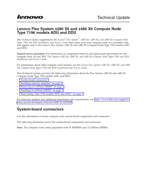
Technical Update Lenovo Flex System x280X6and x480X6Compute Node Type7196models ADU and DDUThis Technical Update supplements the Lenovo®Flex System™x280X6,x480X6,and x880X6Compute Node Types7196and4258Installation and Service Guide that comes with your compute node.It is included with and applies only to the Lenovo Flex System x280X6and x480X6Compute Node Type7196models ADU and DDU.Trained service providers:For instructions on component removal and replacement procedures for this compute node,see the IBM®Flex System x280X6,x480X6,and x880X6Compute Node Types7903and4259 Installation and Service Guide.For information about other compute node features,see the Lenovo Flex System x280X6,x480X6,and x880 X6Compute Node Types7196and4258Installation and Service Guide.This Technical Update provides the following information about the Flex System x280X6and x480X6 Compute Node Type7196models ADU and DDU:v“System-board connectors”v“Installing memory modules”on page2v“Removing an eXFlash DIMM”on page2v“Installing an eXFlash DIMM”on page3v“Parts listing,Type7196models ADU and DDU”on page5For firmware updates and additional information and requirements,see,/support/ entry/portal/docdisplay?lndocid=SERV-FLASHDM.System-board connectorsUse this information to locate compute node system-board components and connectors.The following illustration shows the system-board components and connectors.Note:The compute node comes populated with16RDIMMs and12eXFlash DIMMs.4Micro-1Micro-2Installing memory modulesThe compute node comes populated with 16GB RDIMMs.See “System-board connectors”on page 1for the locations of the DIMM connectors.See Table 1for the DIMM connectors populated with RDIMMs.Table 1.DIMM connectors populated with RDIMMs DIMM connector DIMM connector DIMM connector DIMM connector DIMM 1DIMM 4DIMM 7DIMM 10DIMM 15DIMM 18DIMM 21DIMM 24DIMM 25DIMM 28DIMM 33DIMM 36DIMM 37DIMM 40DIMM 45DIMM 48Removing an eXFlash DIMMUse this information to remove an eXFlash DIMM.Before you beginBefore you remove an eXFlash DIMM,complete the following steps:1.Review the safety information and installation guidelines in the Installation and Service Guide for yourcompute node.22.If the compute node is installed in a Flex System chassis,remove it(see the Installation and ServiceGuide for your compute node for instructions).3.Carefully lay the compute node on a flat,static-protective surface,orienting the compute node withthe bezel pointing toward you.ProcedureTo remove an eXFlash DIMM,complete the following steps.1.Remove the cover(see the Installation and Service Guide for your compute node for instructions).2.Remove the air baffle that is installed over the DIMM connector.3.Locate the DIMM connectors(see“System-board connectors”on page1for the locations of the DIMMconnectors).Determine which eXFlash DIMM you want to remove from the compute node.Attention:To avoid breaking the retaining clips or damaging the DIMM connectors,handle the clips gently.4.Make sure that both retaining clips on the DIMM connector from which you are removing theeXFlash DIMM are in the open position.5.Pull the eXFlash DIMM out of the connector.6.If you are not immediately replacing the eXFlash DIMM,install the air baffle.Attention:v Install the air baffles with the arrow indicating air flow direction pointing to the rear of thecompute node.v To maintain proper system cooling,do not operate the compute node without air baffles installed over the DIMM connectors.What to do nextIf you are instructed to return the eXFlash DIMM,follow all packaging instructions,and use any packaging materials for shipping that are supplied to you.Installing an eXFlash DIMMUse this information to install an eXFlash DIMM.Before you beginBefore you install an eXFlash DIMM,complete the following steps:1.Review the safety information and installation guidelines in the Installation and Service Guide for yourcompute node.2.Read the documentation that comes with the eXFlash DIMMs.3.If the compute node is installed in a Flex System chassis,remove it(see the Installation and ServiceGuide for your compute node for instructions).34.Carefully lay the compute node on a flat,static-protective surface,orienting the compute node withthe bezel pointing toward you.About this taskThe following notes describe information that you must consider when you install eXFlash DIMMs:v The compute node supports 12eXFlash DIMMs only.v Lockstep mode,mirrored-channel mode,and rank sparing are not supported when eXFlash DIMMs are installed.v eXFlash DIMMs operate at the same DIMM frequency as the speed of the RDIMMs installed in the compute node.v eXFlash DIMMs operate only at 1.5V .vFor more information about eXFlash DIMM requirements,see /support/entry/portal/docdisplay?lndocid=SERV-FLASHDM.Note:The amount of eXFlash DIMM storage that is displayed in the Setup utility might be different fromthe amount of eXFlash DIMM storage installed in the compute node.See Table 2for the DIMM connectors populated with eXFlash DIMMs.See “System-board connectors”on page 1for the locations of the DIMM connectors.Table 2.DIMM connectors populated with eXFlash DIMMs DIMM connector DIMM connector DIMM connector DIMM connector DIMM 2DIMM 5DIMM 8DIMM 11DIMM 14DIMM 17DIMM 20DIMM 23DIMM 26DIMM 29DIMM 44DIMM 47ProcedureTo install an eXFlash DIMM,complete the following steps:1.Remove the cover (see the Installation and Service Guide for your compute node for instructions).2.Read the documentation that comes with the eXFlash DIMM.3.Remove the air baffle installed over the DIMM connector.4.Locate the DIMM connectors (see “System-board connectors”on page 1for the locations of theDIMM connectors).Determine in which DIMM connector you want to install the eXFlash DIMM.5.Touch the static-protective package that contains the eXFlash DIMM to any unpainted metal surfaceon the Flex System chassis or any unpainted metal surface on any other grounded rack component in the rack in which you are installing the eXFlash DIMM for at least 2seconds;then,remove the eXFlash DIMM from the package.6.Make sure that both retaining clips on the DIMM connector are in the open position.47.Turn the eXFlash DIMM so that the eXFlash DIMM keys align correctly with the DIMM connectoron the system board.Attention:To avoid breaking the retaining clips or damaging the DIMM connector,handle the clips gently.8.Press the eXFlash DIMM into the DIMM connector.The retaining clips lock the eXFlash DIMM intothe connector.9.Make sure that the small tabs on the retaining clips engage the notches on the eXFlash DIMM.Ifthere is a gap between the eXFlash DIMM and the retaining clips,the eXFlash DIMM has not been correctly installed.Press the eXFlash DIMM firmly into the connector,and then press the retaining clips toward the eXFlash DIMM until the tabs are fully seated.When the eXFlash DIMM is correctly installed,the retaining clips are parallel to the sides of the eXFlash DIMM.10.Install the air baffle over the DIMM connector.Attention:v Install the air baffles with the arrow indicating air flow direction pointing to the rear of thecompute node.v To maintain proper system cooling,do not operate the compute node without air baffles installed over the DIMM connectors.What to do nextAfter you install the eXFlash DIMM,complete the following steps:1.Install the cover onto the compute node(see the Installation and Service Guide for your compute nodefor instructions).2.Install the compute node into the chassis(see the Installation and Service Guide for your compute nodefor instructions).Parts listing,Type7196models ADU and DDUThe following replaceable components are available for the Flex System x280X6and x480X6Compute Node Type7196models ADU and DDU.5Index Description Tier1CRUpart numberFRU partnumber1Top cover(when ordering this part,order the Label Kit part number00MP305)00AG9082Air baffle kit00AG905 3Flex System CN4054R10Gb Virtual Fabric Adapter00Y3309 4Memory,16GB2R x44Gbit DDR-31600MHz1.35V LP RDIMM46W06745Intel Xeon Processor E7-2870V215C2.3GHz30MB Cache1600MHz130W00Y39745Intel Xeon Processor E7-4890V215C2.8GHz37.5MB Cache1600MHz155W44X39986Not available7Bezel,front assembly kit00MP304 8SMP filler00AG911 9Center partition00AG904 10Solid state drive,200GB SAS2.5inch Enterprise MLC G3hot-swap00AJ208 11Hard disk drive backplane,SAS single2.5inch00Y3878 12Heat sink,microprocessor00AG887 Alcohol wipes59P47396Index Description Tier1CRUpart numberFRU partnumberThermal grease kit41Y9292Adapter connector retention kit00AG916Base assembly(includes chassis and system board)00MT370 Label kit00MP305Microprocessor installation tool94Y9971Miscellaneous parts kit00AG910CMOS battery,3.0volt(all models)33F8354CRM handle kit00AG915Rear bulkhead assembly full wide46M2833eXFlash DIMM,400GB SATA MLC00FE0067First Edition(January2015)Copyright Lenovo2015.Portions copyright IBM Corporation2015.LIMITED AND RESTRICTED RIGHTS NOTICE:If data or software is delivered pursuant a General Services Administration“GSA”;contract,use,reproduction,or disclosure is subject to restrictions set forth in Contract No. GS-35F-05925.Lenovo,the Lenovo logo,and Flex System are trademarks of Lenovo in the United States,other countries,or both. Printed in the USA(1P)P/N:00FH395。
VESA E-EDID Standard V1
E-EDID™ Standard VESAVideo Electronics Standards Association860 Hillview Court, Suite 150 Phone: (408) 957-9270 Milpitas, CA 95035 Fax: (408) 957-9277 VESA ENHANCED EXTENDED DISPLAYIDENTIFICATION DATA STANDARDRelease A, Revision 1February 9, 2000PurposeThis standard defines data formats to carry configuration information, allowing optimum use of displays.SummaryThis document describes the basic 128-byte data structure "EDID 1.3", as well as the overall layout of the data blocks that make up Enhanced EDID. The EDID 1.3 data structure is intended to be backward compatible with EDID data structures 1.0, 1.1 and 1.2 as implemented in all commercially available monitors. EDID data structure 1.3 contains enhancements to enable the Dual GTF curve concept. Use of EDID extensions described in this document assumes that the addressing method described in the Enhanced DDC standard is used.GTF: Generalized Timing FormulaNoteThis issue of the EDID document contains specifications for the mandatory core elements of Enhanced EDID. Optional EDID extensions are defined in separate documents.PrefaceIntellectual PropertyCopyright © 1994 - 2000 Video Electronics Standards Association. All rights reserved.While every precaution has been taken in the preparation of this standard, the Video Electronics Standards Association and its contributors assume no responsibility for errors or omissions, and make no warranties, expressed or implied, of functionality or suitability for any purpose.TrademarksAll trademarks used within this document are the property of their respective owners. VESA, DDC, DPMS, EDID, EVC, P&D and VDIF are trademarks of the Video Electronics Standard Association.I2C is a trademark owned by Philips.PatentsVESA proposals and standards are adopted by the Video Electronics Standards Association without regard as to whether their adoption may involve any patents or articles, materials, or processes. Such adoption does not assume any liability to any patent owner, nor does it assume any obligation whatsoever to parties adopting the proposals or standards documents.Support for this StandardClarifications and application notes to support this standard may be written. To obtain the latest standard and any support documentation, contact VESA.If you have a product, which incorporates EDID, you should ask the company that manufactured your product for assistance. If you are a manufacturer, VESA can assist you with any clarification you may require. All comments or reported errors should be submitted in writing to VESA using one of the following methods.•Fax : 408-957 9270, direct this note to Technical Support at VESA•e-mail: support@•mail: TechnicalSupportVideo Electronics Standards Association860 Hillview Court, Suite 15095035CAMilpitas,Revision HistoryRelease A September 2, 1999Initial release of the standard. The body of the standard is derived from the Extended Display Identification Standard Version 3.0Release A Revision 1 February 9, 2000Consolidate requirements of detailed timing section in section 3.10Section 3.4 - removed restriction of 00h, 00h, 00h, 00h value for serial number fieldTable 3.11 - added note to reference preferred timing mode bit requirementsTable 3.15 - added note for 1:1 aspect ratio in earlier EDID definitionsTable 3.16 – corrected order of bits in Vertical Sync format descriptionTable 3.17 - added definition for stereo flag bits values of 0,0,xTable 3.20 - added clarification to round up Max pixel; clock valueAcknowledgmentsThis document would not have been possible without the efforts of the VESA Display Committee. In particular, the following individuals and their companies contributed significant time and knowledge to this edition, and/or previous editions of the EDID document.Anders Frisk Nokia Jack Hosek NECBob Myers HP Richard Atanus NECDon Panell Joe Goodart DellHans van der Ven Panasonic Bill Milford 3dfxGeoff Gould Intel Ian Miller IBMRick Stoneking Microchip Shaun Kerigan IBMGlenn Adler Philips Ed Anwyl IBMChuck Scott Microsoft Anthony Cianfarano MitsubishiAlain d’Hautecourt Viewsonic Ton Wang HitachiWarren Whaley Canon John Matsumoto ToshibaDrew Loucks Elo TouchsystemsTable of ContentsREVISION HISTORY (3)1. OVERVIEW (5)1.1 S UMMARY (5)1.2 B ACKGROUND (5)1.3 S TANDARD O BJECTIVES (5)1.4 R EFERENCE D OCUMENTS (5)2. DATA FORMATS (6)2.1 D ESCRIPTION OF PRESENT AND EARLIER EDID DATA FORMATS (6)2.1.1 EDID1.0 (6)1.1 (6)2.1.2 EDID2.1.3 EDID1.2 (6)1.3 (6)2.1.4 EDID2.0 (6)2.1.5 EDID2.2 E NHANCED EDID (6)2.2.1 Enhanced EDID High Level Layout (7)3. EXTENDED DISPLAY IDENTIFICATION DATA (EDID) STRUCTURE VER. 1 REV. 3 (9)3.1 EDID F ORMAT O VERVIEW (9)3.2 D ATA F ORMAT C ONVENTIONS (10)3.3 H EADER:8 BYTES (11)3.4 V ENDOR/P RODUCT ID:10 BYTES (11)3.5 EDID S TRUCTURE V ERSION /R EVISION:2 BYTES (12)3.6 B ASIC D ISPLAY P ARAMETERS AND F EATURES:5 BYTES (12)3.7 P HOSPHOR OR F ILTER C HROMATICITY:10 BYTES (14)3.8 E STABLISHED T IMINGS:3 BYTES (15)3.8.1 EDID Established Timings Section (15)3.9 S TANDARD T IMING I DENTIFICATION (16)3.9.1 EDID Standard Timings Section (16)3.10 D ETAILED T IMING S ECTION -72 BYTES (17)3.10.1 First Detailed Timing Descriptor Block (17)3.10.2 Detailed Timing Descriptor - 18 bytes (18)3.10.3 MonitorDescription - 18 bytes (19)Descriptor3.11 E XTENSION F LAG AND C HECKSUM (22)3.12 N OTE R EGARDING B ORDERS (23)4. EDID EXTENSIONS (24)5. TIMING INFORMATION PRIORITY ORDER (24)6. APPENDIX A - SAMPLE EDID (25)6.1 EXAMPLE1.E NHANCED EDID SAMPLE WITH S RGB AND S ECONDARY GTF (25)6.2 E XAMPLE 2-L EGACY EDID EXAMPLE FOR REFERENCE (28)7. APPENDIX B - ANSWERS TO COMMONLY ASKED QUESTIONS (31)1.OVERVIEW1.1SummaryThe Extended Display Identification Data (EDID) described in this document, is a data structure, with optional variants, to allow the display to inform the host about its identity and capabilities. The EDID data structure is independent of the communication protocol used between the monitor and host.Enhanced EDID defines a basic data structure of 128 bytes that all compliant monitors must supply, as well as the rules for how extensions can be added to the basic structure.Enhanced EDID family of documents:1 Enhanced EDID Standard (Basic 128-byte data structure. Rules for how EDID extensions are mapped.)2 Optional EDID Extension Standards (Data structure for additional data contained in EDID extensions.)2.1EDID Structure 2 Extension2.2Flat Panel Timings Extension2.3Color transfer function Extension2.4…future extension structures not yet defined1.2BackgroundEnhanced EDID was created to clarify how EDID Extensions shall be used in order to handle identification of future monitor capabilities, while maintaining a basic level of compatibility that can be used to uniquely identify the monitor. Enhanced EDID is intended to supersede all previous versions of EDID.1.3Standard ObjectivesThe EDID Standard was developed by VESA to meet, exceed and/or complement certain criteria. These criteria are set forth as Standard Objectives as follows:•Support Microsoft® Plug and Play definition•Provide information in a compact format to allow the graphics subsystem to be configured based on the capabilities of the attached display1.4Reference DocumentsNote: Versions identified here are current, but users of this standard are advised to ensure they have the latest versions of referenced standards and documents.2.DATA FORMATS2.1Description of present and earlier EDID data formats2.1.1EDID 1.0EDID structure 1.0 was the original 128-byte data format introduced in the DDC Standard Version 1.0 Revision 0 issued in August 1994. EDID 1.0 shall not be used in new monitor designs released after January 1, 2000.2.1.2EDID 1.1EDID structure 1.1 added definitions for monitor descriptors as an alternate use of the space originally reserved for detailed timings, as well as definitions for previously unused fields. Structure 1.1 was introduced in the EDID Standard Version 2 Revision 0 issued in April 1996. EDID 1.1 shall not be used in new monitor designs released after January 1, 2000.2.1.3EDID 1.2EDID structure 1.2 added definitions to existing data fields. Structure 1.2 was introduced in EDID Standard Version 3. EDID 1.2 is not recommended in new monitor designs released after January 1, 2000.2.1.4EDID 1.3EDID structure 1.3 is introduced for the first time in this document and adds definitions for secondary GTF curve coefficients. EDID 1.3 is based on the same core as all other EDID 1.x structures. EDID 1.3 is intended to be the new baseline for EDID data structures. EDID 1.3 is recommended for all new monitor designs.Structure 1.3 is a super set of structure 1.2. The main difference between the two is that 1.3 allows the Monitor Range Limits descriptor to define coefficients for a secondary GTF curve, and mandates a certain set of monitor descriptors.2.1.5 EDID 2.0Version 2 Revision 0 data structure defined a completely new EDID data structure based on 256-byte records. This structure was designed to provide additional information that is required for displays that follow the original VESA Plug & Display (P&D) and Flat Panel Display Interface-2 (FPDI-2) Standards.NOTE! In the future, EDID structure 2.0 will be treated as an allowed, but not mandatory, EDID extension under Enhanced EDID.2.2Enhanced EDID2.2.1Enhanced EDID High Level Layout2.2.1.1Mandatory elementsBlock 0 is the only mandatory block.Each extension block is structured according to Section 2.2.1.3.All extension blocks must be sequential, no holes allowedBlock # Block Description0 EDID 1.3 (or higher)1 Extension if only 1 extension, otherwiseEDID Block map (blocks 2-127)2 Extension3 Extension4 Extension:N Extension:128 EDID Block map for blocks 129 – 254 ifmore than 128 blocks used129 Extension:N =< 254 ExtensionBlock number 1 is used for Extension data if there is only one extension, otherwise block 1 is used as a block map.2.2.1.2EDID Block Map ExtensionByte # Description0 Tag for Block Map1 Extension Tag for data in block2 or block 129 Unused blocks are listed as Extension Tag = 02 Extension Tag for data in block3 or block 130N Extension Tag for data in blockN+1 or block N+128126 Extension Tag for data in block127 or block 254127 Check sum for this block mapBlock Tag is a byte that identifies the content of the Extension Block. A partial list of defined Tags is listed in Section 2.2.1.4.2.2.1.3General Extension FormatByte # DescriptionTag0 Extension1 Revision number for this tag One byte binary number. Revisions arebackward compatible.data2-126 Extension127 Checksum for this ExtensionBlock2.2.1.4EDID Extension Tags Assigned by VESAVESA will maintain a list of assigned EDID Extension Tags used to identify VESA Standard EDID Extensions. For the most current list of EDID Extensions, see the VESA website.Tag DescriptionTimings01h LCD02h Additional timing data type 220h EDID 2.0 Extension30h Color information type 040h DVI feature data50h Touch screen dataF0h Block MapFFh Extension defined by monitor manufacturer.Note: At the time of the publication of this document, several of these extensions were not yet been defined or written. Contact VESA administration for the latest list of published EDID Extensions.3.Extended Display Identification Data (EDID) Structure Ver. 1 Rev. 33.1EDID Format Overviewbytes Description Format Address No.00h 8 Bytes Header See Section 3.300h00h 1FFh01h 1FFh02h 1FFh03h 1FFh04h 1FFh05h 1FFh06h 100h07h 108h 10 Bytes Vendor / Product Identification See Section 3.408h 2 ID Manufacturer Name EISA 3-character ID0Ah 2 ID Product Code Vendor assigned code0Ch 4 ID Serial Number 32-bit serial number10h 1 Week of Manufacture Week number11h 1 Year of Manufacture Year12h 2 Bytes EDID Structure Version / Revision See Section 3.5# Binary12h 1Version# Binary13h 1Revision14h 5 Bytes Basic Display Parameters / Features See Section 3.614h 1 Video Input Definition15h 1 Max. Horizontal Image Size cm.16h 1 Max. Vertical Image Size cm.17h 1 Display Transfer Characteristic (Gamma) Binary18h 1 Feature Support See Table 3.1119h 10 Bytes Color Characteristics See Section 3.719h 1 Red/Green Low Bits Rx1 Rx0 Ry1 Ry0 Gx1 Gx0 Gy1Gy0 1Ah 1 Blue/White Low Bits Bx1 Bx0 By1 By0 Wx1 Wx0 Wy1Wy01Bh 1 Red-x Red-x Bits 9 - 21Ch 1 Red-y Red-y Bits 9 - 21Dh 1 Green-x Green-x Bits 9 - 21Eh 1 Green-y Green-y Bits 9 - 21Fh 1 Blue-x Blue-x Bits 9 - 220h 1 Blue-y Blue-y Bits 9 - 221h 1 White-x White-x Bits 9 - 222h 1 White-y White-y Bits 9 - 223h 3 Bytes Established Timings See Section 3.823h 1 Established Timings 124h 1 Established Timings 225h 1 Manufacturer's Reserved Timings26h 16 Bytes Standard Timing Identification See Section 3.926h 2 Standard Timing Identification # 128h 2 Standard Timing Identification # 22Ah 2 Standard Timing Identification # 32Ch 2 Standard Timing Identification # 42Eh 2 Standard Timing Identification # 530h 2 Standard Timing Identification # 6Address No.bytes Description Format32h 2 Standard Timing Identification # 734h 2 Standard Timing Identification # 836h 72 Bytes Detailed Timing Descriptions See Section 3.1036h 18 Detailed Timing Description # 1 EDID structure Version 1, Revisions 1and 2, allowed this space to be used forMonitor Descriptors. Host SW usingthis data should be prepared to detectMonitor Descriptors also in thislocation even though displaysconforming with later revisions ofEDID structure only use this space forDetailed Timing Description.48h 18 Detailed Timing Description # 2 orMonitor Descriptor5Ah 18 Detailed Timing Description # 3 orMonitor Descriptor6Ch 18 Detailed Timing Description # 4 orMonitor Descriptor7Eh 1 Byte Extension Flag Number of (optional) 128-byte EDIDextension blocks to follow.7Fh 1 Byte Checksum The 1-byte sum of all 128 bytes in thisEDID block shall equal zeroTable 3.1 - EDID Structure Version 1The following sections provide details on each byte of the EDID Version 1 data structure.3.2Data Format ConventionsThe EDID data structures are designed to be compact in their representation of data in order to fit the most information into a limited space. To accommodate this, many data lengths have been used according to the needs of the particular data. These include fields from a single bit up to two bytes in length. In all cases, except where explicitly stated, the following conventions are used:Data length Convention used Example1 to 7 bits stored in order stated8 bits (1 byte) stored at location stated9 to 15 bits location of bits stated in field definition16 bits (2 bytes) Bytes are a binary format (not BCD) stored inlocations specified with least significant byte(LSB) stored in first location. 1280 decimal = 0500h Stored 00 at first location 50 next locationCharacter string (More than 2 bytes) Bytes are ASCII, stored in order they appearin the string.“ACED”Stored 41h at first location,43h at the next location, 45h atthe next location and 44h at thenext location.Table 3.2 - Data Format Conventions3.3Header: 8 bytesThe header is an 8-byte pattern designed to be easily recognizable from other bytes in the data structure. Its format is shown in Table 3.3.8 Bytes Header1 00h1 FFh1 FFh1 FFh1 FFh1 FFh1 FFh1 00hTable 3.3 - EDID Header3.4Vendor/Product ID: 10 bytesThe Vendor/Product ID block is made up of several fields used to uniquely identify the monitor. The size and order of the fields is shown in the table below.10 Bytes Vendor / Product Identification2 ID Manufacturer Name2 ID Product Code4 ID Serial Number1 Week of Manufacture1 Year of ManufactureTable 3.4 - Vendor/Product IDThe ID Manufacturer Name field, shown in Table 3.5, contains a 2-byte representation of the monitor's manufacturer. This is the same as the EISA ID. It is based on compressed ASCII, “0001=A” ... “11010=Z”.EISA manufacturer IDs are issued by Microsoft. Contact by:E-mail: pnpid@Fax: 425-936-7329, Attention PNPID in Building 27.Description Byte Bit7 6 5 4 3 2 1 0ID Manufacturer Name 1 0) (4 3 2 1 0) (4 3* Character 1 Char 22 2 1 0) (43 2 1 0)Character 2 Character 3Table 3.5 - ID Manufacturer NameThe ID Product code field contains a 2-byte vendor assigned product code. This is used to differentiate between different models from the same manufacturer. If this field is used to represent a model number, then the number is stored in hex with the least significant byte first.A 00001 41B 00010 42C 00011 43D 00100 44E 00101 45F 00110 46G 00111 47H 01000 48N 01110 4E O 01111 4F P 10000 50 Q 10001 51 R 10010 52 S 10011 53 T 10100 54 U 10101 55压缩ASCII ASCII ASCII压缩ASCII应为00001The ID serial number is a 32-bit serial number used to differentiate between individual instances of the same model of monitor. Its use is optional. When used, the bit order for this field follows that shown in Table 3.6. The EDID structure Version 1 Revision 1 and later offer a way to represent the serial number of the monitor as an ASCII string in a separate descriptor block.1 Bit2 Bit4 Bit3 BitDescription Byte Bit 7 Bit 6 Bit 5 BitNumber 1 (7 6 5 4 3 2 1 0) IDSerial2 (15 14 13 12 11 10 9 8)3 (23 22 21 20 19 18 17 16)4 (31 30 29 28 27 26 25 24)Table 3.6 - ID Serial NumberThe Week of Manufacture field, if used, is set to a value in the range of 1-53. If this field is not used, the value should be set to 0.The Year of Manufacture field is used to represent the year of the monitor’s manufacture. The value that is stored is an offset from the year 1990 as derived from the following equation:Value stored = (Year of manufacture - 1990)Example: For a monitor manufactured in 1997 the value stored in this field would be 7.3.5EDID Structure Version / Revision: 2 bytes2 Bytes EDID Structure Version, Revision1 Version no. Binaryno. Binary1 RevisionTable 3.7 - EDID Structure Version and RevisionThe appropriate version and revision numbers shall be stored here. These values define the EDID structure being used. Products compliant with this document shall have Version = 1 and Revision = 3.3.6Basic Display Parameters and Features: 5 bytes5 Bytes Basic Display Parameters/Features1 Video Input Definition See Table 3.91 Max. Horizontal Image Size cm.1 Max. Vertical Image Size cm.Characteristic (Gamma) (gamma x 100)-100, [range 1.00 → 3.54]Transfer1 DisplayIf set to FFh, the gamma value is notdefined here.1 Feature Support (DPMS) See Table 3.11Table 3.8 - Basic Display Parameters and FeaturesThe Video Input Definition field provides information describing how the host’s video outputs should be configured to drive the attached display. The format of this one-byte field is described below in Table 3.9 Bit Description DetailedDescription7 Analog/Digital Signal Level Defines usage of the rest of byte as “analog” or “digital” input.Analog = 0, Digital = 1.If bit 7 = 0 use the following definitions for bit 6-06 Signal Level Standard [6:5] Refer to following definitions. Format is ‘reference white aboveblank’, ‘level of sync. tip below blank’. (volts)Bit 6 Bit 5 Operation0 0 0.700, 0.300 (1.000 V p-p)0 1 0.714, 0.286 (1.000 V p-p)1 0 1.000, 0.400 (1.400 V p-p)1 1 0.700, 0.000 (0.700 V p-p) See EVC Std.5 Signal Level Standard [6:5] See above entry for definition4 Setup If set = 1, the display expects a blank-to-black setup or pedestalper appropriate Signal Level Standard3 Sync. Inputs Supported [3] If set = 1, separate syncs. supported2 Sync. Inputs Supported [2] If set = 1, composite sync. (on Hsync line) supported1 Sync. Inputs Supported [1] If set = 1, sync. on green video supported0 Sync. Inputs Supported [0] If set = 1, serration of the Vsync. Pulse is required whencomposite sync. or sync-on-green video is used If bit 7 = 1 use the following definitions for bit 6-06-1 Reserved Set all reserved bits to 00 DFP 1.x If set = 1, Interface is signal compatible with VESA DFP 1.xTMDS CRGB, 1 pixel / clock, up to 8 bits / color MSB aligned,DE active highTable 3.9 - Video Input DefinitionThe Maximum Image Size parameters provide information on the maximum image dimensions that can be correctly displayed, as defined by VESA Video Image Area Definition (VIAD) Standard, rounded to the nearest centimeter (cm). These values are intended to be the maximum image size that can be properly displayed over the entire set of supported timing/format combinations. The host system is expected to use this data to get a rough idea of the image size and aspect ratio to allow properly scaled text to be selected.If either or both bytes are set to zero, then the system shall make no assumptions regarding the display size.e.g. A projection display may be of indeterminate size.2 Bytes Description Format1 Max.HorizontalImage Size From 1 → 255 cmSee above for special case = 01 Max. Vertical Imagesize From 1 → 255 cmSee above for special case = 0Table 3.10 - Maximum Image SizeThe display transfer characteristic, referred to as gamma, is stored in a 1-byte field capable of representing gamma values in the range of 1.00 to 3.54. The integer value stored is determined by the formula: Value stored = (gamma x 100)-100 For example, a gamma value of 2.2 would be represented as 120.The feature support field is used to indicate support for various display features. The format of this 1-byte field is shown in following table.1 Byte Bits Feature Support Description1 7 Standby Refer to VESA DPMS Specification6 Suspend Refer to VESA DPMS Specification5 Active Off/Very Low Power The display consumes much lesspower when it receives a timingsignal that is outside its declaredactive operating range.The display will revert to normaloperation if the timing signal returnsto the normal operating range.No sync. signals is one example of atiming signal outside normaloperating range.No DE signal is another example.4-3 Display Type [4:3] Bit 4 Bit 3 Interpretation0 0 Monochrome /grayscale display0 1 RGB color display1 0 Non-RGB multicolordisplaye.g. R/G/Y1 1 Undefined2 Standard Default Color Space, sRGB If this bit is set to 1, the display usesthe sRGB standard default colorspace as its primary color space. Ifthis bit is set, the color information insection 3.7 must match the sRGBstandard values. (See example inAppendix A)1 Preferred Timing Mode If this bit is set to 1, the display’spreferred timing mode is indicated inthe first detailed timing block.Note: Use of preferred timing modeis required by EDID StructureVersion 1 Revision 3 and higher.0 Default GTF supported If this bit is set to 1, the displaysupports timings based on the GTFstandard using default GTF parametervalues.Table 3.11 - Feature Support3.7 Phosphor or Filter Chromaticity: 10 bytesThese bytes provide colorimetry and white point information. The data is stored in the order shown in Table 3.12.The white point value shall be the default white point (the white point set at power on or on a reset of the display to its default setting). Provision for multiple white points is made in one of the monitor descriptors - see Section3.10.3.10 Bytes Color Characteristic Based on CIE publication 15.2 oncolorimetry space1 Red / Green Low Bits Rx1 Rx0 Ry1 Ry0 Gx1 Gx0 Gy1 Gy01 Blue / White Low Bits Bx1 Bx0 By1 By0 Wx1 Wx0 Wy1 Wy01 Red_x Red_x bits 9 → 21 Red_y Red_y bits 9 → 21 Green_x Green_x bits 9 → 21 Green_y Green_y bits 9 → 21 Blue_x Blue_x bits 9 → 21 Blue_y Blue_y bits 9 → 21 White_x White_x bits 9 → 21 White_y White_y bits 9 → 2Table 3.12 - Chromaticity and Default White PointThe chromaticity and white point values are expressed as fractional numbers, accurate to the thousandth place. Each number is represented by a binary fraction, which is 10 bits in length. In this fraction a value of one for the bit immediately right of the decimal point (bit 9) represents 2 raised to the -1 power. A value to 1 in the right most bit (bit 0) represents a value of 2 raised to the -10 power.The high order bits (9 → 2) are stored as a single byte. The low order bits (1 → 0) are paired with other low order bits to form a byte. With this representation, all values should be accurate to +/- 0.0005 of the actual value. Examples are shown in Table 3.13.Actual Value Binary value Converted Back to Decimal0.610 1001110001 0.61035160.307 010******* 0.30664060.150 0010011010 0.1503906Table 3.13 - Ten bit Binary Fraction Representation3.8Established Timings: 3 bytesThe established timing block is a field of one-bit flags, which are used to indicate support for established VESA and other common timings in a very compact form. Other standardized timings can be described in the Standard Timings block defined in Section 3.9. Any timing can be described using the Detailed Timings block defined in Section 3.10.Bits 6 → 0 (inclusive) of byte 3 are used to define manufacturer’s proprietary timings, and may be used if a manufacturer wants to identify such timings through the use of one-bit flags. VESA takes no responsibility for coordinating or documenting the use of these bits by any manufacturer(s).A bit set to “1” indicates support for that timing.3.8.1EDID Established Timings SectionIndicates Factory Supported Modes of VESA Discrete Monitor Timings (DMTs that predated EDID) as well as other industry de-facto timings that predate EDID. The one-bit flags of the Established Timing block can not be used to determine maximum format support, maximum refresh support, or any other timing parameter of the display. Also, if any one-bit flag is not set in the Established Timing block, this data can not be used to determine if that timing is within the supported scanning frequency of the display - only that it is not a Factory Supported Mode.Factory Supported Modes are defined as modes that are properly sized and centered as the monitor is delivered from factory.All Factory Supported Modes are not necessarily listed in any EDID timing section.3 Bytes Bit Description Source1 Established Timing I7 720 x 400 @ 70Hz IBM, VGA6 720 x 400 @ 88Hz IBM, XGA25 640 x 480 @ 60Hz IBM, VGA4 640 x 480 @ 67Hz Apple, Mac II3 640 x 480 @ 72Hz VESA2 640 x 480 @ 75Hz VESA1 800 x 600 @ 56Hz VESA0 800 x 600 @ 60Hz VESA1 Established Timing II7 800 x 600 @ 72Hz VESA6 800 x 600 @ 75Hz VESA5 832 x 624 @ 75Hz Apple, Mac II4 1024 x 768 @ 87Hz(I) IBM3 1024 x 768 @ 60Hz VESA2 1024 x 768 @ 70Hz VESA1 1024 x 768 @ 75Hz VESA0 1280 x 1024 @ 75Hz VESATimings1 Manufacturer's7 1152 x 870 @ 75Hz Apple, Mac IIReserved6-0Table 3.14 - Established Timings3.9Standard Timing IdentificationThe next 16 bytes provide identification for up to eight additional timings, each identified by a unique 2-byte code derived from the mode format and refresh rate as described below. This scheme is used to identify future standard timings not included in the Established Timings section (see Section 3.8). Standard Timing identifiers that don’t correspond to a VESA Discrete Monitor Timing Mode are referring to a mode calculated using the VESA GTF with default coefficients. The scheme may also be used in monitors intended to be used exclusively with proprietary systems where the host already has the complete timing information. Additional standard timings may be listed by using one of the alternate definitions of the detailed Timing Descriptions permitted in EDID Structure Version 1, Revision 1 and higher - see Section 3.10.3.Note: The 2-byte identifier codes for VESA standard timing modes are defined as part of each VESA Timing Standard.Unused fields in this section shall be set to 01h, 01h.3.9.1EDID Standard Timings SectionThe Standard Timings section is used to identify Factory Supported Modes that fall into one or both of two categories:1.VESA Discrete Monitor Timings (listed in the VESA DMT Standards document) not included in the currentEstablished Timing section.2.Discrete timing modes calculated using GTF.A 2-byte timing identifier identifies each timing mode. If a timing identifier listed corresponds to an issued VESA Discrete Monitor Timing, factory adjustment data must be stored (preset) in the display. If a timing identifier listed does not match a VESA DMT identifier, it shall refer to a timing calculated using the Generalized Timing Formula (GTF.)Factory Supported Modes are defined as modes that are properly sized and centered as the monitor is delivered from the factory.。
sn65hvd230中文用户手册

Changes from Revision K (February 2011) to Revision L
Page
• 已添加 引脚配置和功能部分,ESD 额定值表,特性描述部分,器件功能模式,应用和实施部分,电源相关建议部分, 布局部分,器件和文档支持部分以及机械、封装和可订购信息部分........................................................................................ 1
11 应用和实施 ............................................................ 24 11.1 应用信息................................................................ 24 11.2 典型应用................................................................ 24 11.3 系统示例................................................................ 28
10 详细说明 ................................................................ 18 10.1 概要 ....................................................................... 18 10.2 功能框图................................................................ 18 10.3 特性描述................................................................ 19 10.4 器件功能模式......................................................... 19
工厂检验报告样本CIG023

CIG 023Factory InspectionReport ChineseUL does not endorse any vendors or products referenced herein.UNDERWRITERS LABORATORIES INC. ASSUMES NO RESPONSIBILITY FOR ANY OMISSIONS OR ERRORS ORINACCURACIES WITH RESPECT TO THIS INFORMATION. UL MAKES NO REPRESENTATION OR WARRANTY OF ANY KIND WHATSOEVER, WHETHER EXPRESS OR IMPLIED, WITH RESPECT TO THE ACCURACY, CONDITION, QUALITY, DESCRIPTION, OR SUITABILITY OF THIS INFORMATION, INCLUDING ANY WARRANTY OF MERCHANTABILITY OR FITNESS FOR A PARTICULAR PURPOSE AND EXPRESSLY DISCLAIMS THE SAME.Copyright Underwriters Laboratories Inc. All rights reserved. May not be reproduced without permission. This document isWARNING:THIS DOCUMENT IS ONLY VALID IF USED BY ECS MEMBERSAND THEIR AUTHORISED AGENTSPERMANENT DOCUMENT 永久性文件CIG 023Factory Inspection Report 工厂检验报告WARNING:THIS DOCUMENT IS ONLY VALID IF USED BY ECS MEMBERSAND THEIR AUTHORISED AGENTS警告:本文件仅在为欧洲认证体系(ECS)成员及其授权代理人所用时生效Approved by: ECS General Meeting, 22/23-04-2009 Nr of pages: 19 Date of issue: May 2009Supersedes: PD CIG 023 - June 2004 Page 1 of 19 PD CIG 023 reports shall not contain any unauthorised modifications which change the originalmeaning or the requirements.Any additions created to any document in the series shall be shown in an Appendix.未经批准,不得对 PD CIG 023 报告进行任何改变其原有含意或要求的修改。
- 1、下载文档前请自行甄别文档内容的完整性,平台不提供额外的编辑、内容补充、找答案等附加服务。
- 2、"仅部分预览"的文档,不可在线预览部分如存在完整性等问题,可反馈申请退款(可完整预览的文档不适用该条件!)。
- 3、如文档侵犯您的权益,请联系客服反馈,我们会尽快为您处理(人工客服工作时间:9:00-18:30)。
BRICS RS-99-49 Ageev & Sviridenko: An Approximation Algorithm for Hypergraph Max k -CutBRICS ISSN0909-0878December1999Copyright c 1999,Alexander A.Ageev&Maxim I.Sviridenko.BRICS,Department of Computer ScienceUniversity of Aarhus.All rights reserved.Reproduction of all or part of this workis permitted for educational or research useon condition that this copyright notice isincluded in any copy.See back inner page for a list of recent BRICS Report Series publications. Copies may be obtained by contacting:BRICSDepartment of Computer ScienceUniversity of AarhusNy Munkegade,building540DK–8000Aarhus CDenmarkTelephone:+4589423360Telefax:+4589423255Internet:BRICS@brics.dkBRICS publications are in general accessible through the World Wide Web and anonymous FTP through these URLs:http://www.brics.dkftp://ftp.brics.dkThis document in subdirectory RS/99/49/An Approximation Algorithm for HypergraphMax k -Cut with Given Sizes of Parts Alexander A.AgeevSobolev Instituteof MathematicsNovosibirsk,Russiaageev@math.nsc.ru Maxim I.Sviridenko BRICS University of Aarhus Aarhus,Denmark sviri@brics.dkBRICS ∗1IntroductionProbably most of the recent striking breakthroughs in designing approxima-tion algorithms with provable performance guarantees are due to using novel methods of rounding polynomially solvable fractional relaxations.Applica-bility of the known rounding methods is highly dependent on the type of the constraints in such relaxations.In [1]the authors presented a new rounding (pipage)method especially oriented to tackle some NP-hard problems which can be equivalently reformulated as integer programs with cardinality or a bit more general constraints.The paper [1]contains four results demonstrating the strength of the pipage rounding.One of them is an 1/2-approximation algorithm for Max k -Cut with given sizes of parts.An instance of this prob-lem consists of an undirected graph G =(V,E ),a collection of nonnegativeweights w e associated with its edges and k positive integers p 1,p 2,...,p k such that k i =1p i =|V |.It is required to find a partition of V into k parts V 1,V 2,...,V k with each part V i having size p i so as to maximize the totalweight of edges whose ends lie in different parts of the partition.The Max Cut and Max k -Cut problems are classical in combinatorial optimization and have been extensively studied in the absence of cardinality constraints.The best known approximation algorithm for Max Cut is due to Goemans and Williamson [8]and has performance guarantee of 0.878.Frieze and Jerrum[7]extended the technique of Goemans and Williamson to Max k -Cut and designed a (1−1/k +2ln k/k 2)-approximation algorithm.Few approximation algorithms are known for some special cases of Max k -Cut with given sizes of parts.In particular,Frieze and Jerrum [7]present an 0.65-approximation algorithm for Max Bisection (in this problem k =2and p 1=p 2=|V |/2).Very recently,Ye [9]announced an algorithm with a better performance guar-antee of 0.699.The best known approximation algorithm for Max k -Section (in this problem p 1=···=p k =|V |/k )is due to Andersson [2]and has performance guarantee of 1−1/k +Θ(1/k 3).In this paper we consider a natural hypergraph generalization of Max k -Cut with given sizes of parts —Hypergraph Max k -Cut with given sizes of parts (HMkC for short).An instance of HMkC consists of a hypergraph H =(V,E ),a collection of non-negative weights w S on its edges S ,and k positive integers p 1,...,p k such that k i =1p i =|V |.It is required to partition the vertex set V into k parts (X 1,...,X k )with |X i |=p i for each i ,so as to maximize the total weight of edges of H not lying wholly in any part of the partition (that is,to max-imize the total weight of edges S such that S \X i =∅for each i ).Several closely related versions of Hypergraph Max k -Cut were studied in the liter-ature but very few results have been obtained.Andersson and Engebretsen[3]presented an 0.72-approximation algorithm for the ordinary Hypergraph Max Cut problem.Arora,Karger and Karpinski [4]designed a PTAS for dense instances of this problem (i.e.in the case of hypergraphs H having Θ(|V (H )|d )edges)under the condition that |S |≤d for each edge S and some constant d .In this paper by applying the pipage rounding method we prove that HMkC can be approximated within a factor of min {λ|S |:S ∈E }of the optimum where λr =1−(1−1/r )r −(1/r )r .By direct calculations it easy to get some specific values of λr :λ2=1/2,λ3=2/3≈0.666,λ4=87/128≈0.679,λ5=84/125=0.672,λ6≈0.665and so on.It is clear that λr tends to 1−e −1≈0.632as r →∞.A less trivial fact is that λr >1−e −1for each r ≥3(Lemma 2in this paper).Adding up we arrive at the following conclusions:our algorithm finds a feasible cut of weight within a factor of 1/2on general hypergraphs (we assume that each edge in a hypergraph has2size at least2),and within a factor of1−e−1in the case when each edge has size at least3.Note that thefirst bound coincides with that we obtained in[1]for the case of graphs.In this paper we also show that in the case of hypergraphs without two-vertex edges the bound of1−e−1cannot be improved unless P=NP.2Pipage rounding:a general schemeWe begin with a description of the pipage rounding method[1]in the case of a slightly more general constraints.Assume that a problem P can be reformulated as the following nonlinear binary program:max F(x11,...,x nk)(1)s.t.ni=1x it=p t,t=1,...,k,(2) kt=1x it=1,i=1,...,n,(3) x it∈{0,1},t=1,...,k,i=1,...,n(4)where p1,p2,...,p k are positive integers such thattp t=n,F(x)is afunction defined on the rational points x=(x it)of the n×k-dimensional cube[0,1]n×k and computable in polynomial time.Assume further that one can associate with F(x)another function L(x)which is defined and polynomially computable on the same set,coincides with F(x)on binary x satisfying(2)–(3),and the program(which we call a nice relaxation)max L(x)(5)s.t.ni=1x it=p t,t=1,...,k,(6) kt=1x it=1,i=1,...,n,(7) 0≤x it≤1,t=1,...,k,i=1,...,n(8)is polynomially solvable.Assume next that the following two main conditions hold.Thefirst—F/L-lowerbound condition—states:there exists C>03such that F(x)/L(x)≥C for each x∈[0,1]n×k.To formulate the second—ε-convexity condition—we need a description of the so-called pipage step.Let x be a feasible solution to(5)–(8).Define the bipartite graph H withthe bipartition({1,...,n},{1,...,k})so that jt∈E(H)if and only if x jtis fractional.Note that(6)and(7)imply that each vertex of H is eitherisolated or has degree at least2.Assume that x has fractional components.Since H is bipartite it follows that H has a cycle C of even length.Let M1and M2be the matchings of H whose union is the cycle C.Define a newsolution x(ε)by the following rule:if jt is not an edge of C,then x jt(ε)coincides with x jt,otherwise,x jt(ε)=x jt+εif jt∈M1,and x jt(ε)=x jt−εif jt∈M2.By definition x(ε)is a feasible solution to the linear relaxation of(5)–(8)for allε∈[−ε1,ε2]whereε1=min{minjt∈M1x jt,minjt∈M2(1−x jt)}andε2=min{minjt∈M1(1−x jt),minjt∈M2x jt}.Theε-convexity condition states that for each feasible x and each cycle C in the graph H,ϕ(ε)=F(x(ε))is a convex function on the above interval.Under the above assumptions we claim that there exists a polynomial-time C-approximation algorithm for solving P.Indeed,since the function ϕ(ε)=F(x(ε))is convex,F(x(ε∗))≥F(x)≥CL(x)for someε∗∈{−ε1,ε2}.The new solution x(ε∗),being feasible for(5)–(8), has a smaller number of fractional components.Set x =x(ε∗)and,if x has fractional components,apply to x the above described pipage step and so on.Ultimately,after at most nk steps,we arrive at a solution˜x which is feasible for(1)–(4)and satisfiesF(˜x)≥CL(x)≥CF∗where F∗is an optimal value of(1)–(4)(and of the original problem P). Thus we obtain a C-approximation algorithm for P.43Pipage rounding:Hypergraph Max k-Cut with given sizes of partsIt is easy to see that an instance of HMkC can be reformulated as the fol-lowing(nonlinear)integer program:max F(x)=S∈E w S1−kt=1i∈Sx it(9)s.t.kt=1x it=1,for each i,(10) ni=1x it=p t,for all t,(11) x it∈{0,1},for each i and t.(12)The equivalence is shown by the one-to-one correspondence between optimal solutions to the above program and optimal k-cuts{X1,...,X k}of instance of HMkC defined by the relation“x it=1if and only if i∈X t”.We claim that for each feasible x and each cycle C in the graph H(for definitions,see Section2)the functionϕ(ε)=F(x(ε))is a quadratic polyno-mial with a nonnegative main coefficient.Indeed,observe that each producti∈S x it(ε)contains at most two modified variables.Assume that a producti∈S x it(ε)contains exactly two such variables x i1t(ε)and x i2t(ε).Then theymay have only one of the following forms:either x i1t +εand x i2t−εor x i1t−εand x i2t +ε,respectively.In either caseε2has a nonnegative coefficient in theterm corresponding to the product.Thus theε-convexity condition holds.As a nice relaxation we consider the following linear program:5maxS∈Ew S z S(13) s.t.z S≤|S|−i∈Sx it for each S∈E,(14)kt=1x it=1for each i,(15)ni=1x it=p t for each t,(16)0≤x it≤1for each i and each t,(17)0≤z S≤1for each S∈E.(18) It is easy to see that,given a feasible matrix x,the optimal values of z S in the above program can be determined by simple ing this observation we can exclude the variables z S and rewrite(13)–(18)in the following equivalent way:max L(x)=S∈E w S min{1,mint(|S|−i∈Sx it)}(19)subject to(15)–(17).Note that F(x)=L(x)for each x satisfying(10)–(12).For any r≥1,setλr=1−(1−1/r)r−(1/r)r.Lemma1.Let x=(x it)be a feasible solution to(19),(15)–(17)and S∈E.Then1−kt=1i∈Sx it≥λ|S|min{1,mint(|S|−i∈Sx it)}.Proof.Let z S=min{1,min t(|S|−i∈Sx it)}.Define q S and t by the equal-itiesq S=maxti∈Sx it=i∈Sx it .Note thatz S=min{1,|S|−q S}.(20)6Using the arithmetic-geometric mean inequality and the fact thatk t=1i∈Sx it=|S|we obtain that1−kt=1i∈Sx it=1−i∈Sx it −t=ti∈Sx it≥1−i∈Sx it|S||S|≥1−qS|S||S|=1−qS|S||S|=1−qS|S||S|.(21)Letψ(y)=1−1−y|S||S|.Case1.|S|−1≤q S≤|S|.Then by(20),z S=|S|−q S and by(21),1−kt=1i∈Sx it≥1−1−z S|S||S|.Since the functionψis concave andψ(0)=0,ψ(1)=λ|S|,it follows that1−kt=1i∈Sx it≥λ|S|z S.Case2.1≤q S≤|S|−1.Here z S=1.Sinceψ(y)is concave andψ(1)=ψ(|S|−1)=λ|S|,1−kt=1i∈Sx it≥λ|S|.7Case3.0≤q S≤1.Again,z S=1.Letµt=i∈Sx it for each t.Note that,by the assumption of the case,0≤µt≤1,(22) and,moreover,kt=1µt=|S|.(23) By the arithmetic-geometric mean inequality it follows thatk t=1i∈Sx it≤kt=1µt|S||S|=1− 1|S||S|≥1− 1|S||S|=λ|S|.Corollary1.Let x=(x it)be a feasible solution to(19),(15)–(17).ThenF(x)≥(minS∈Eλ|S|)L(x).The corollary states that the F/L-lowerbound condition holds with C= min S∈Eλ|S|and thus,by applying the pipage rounding we obtain an al-gorithm whichfinds a feasible k-cut whose weight is within a factor of min S∈Eλ|S|of the optimum.Note thatλ2=1/2.8Lemma2.For any r≥3,λr>1−e−1.Proof.Wefirst deduce it from the following stronger inequality:1−12rfor all r≥1.(24)Indeed,for any r≥3,λr=1−1rr>1−12r=1−e−1+12−1r )<l n(1−1iwe obtain that for each r=1,2,...,1+r ln1−1r−13r3−...=−13r2−12r−13(2r)3...=ln(1−1We now show that the integrality gap ratio for the relaxation(15)–(18) can be arbitrarily close toλr in the case of r-uniform hypergraphs.It follows that there is no chance to get a better bound by applying any rounding method to this relaxation.Indeed,consider the following instance:the complete r-uniform hyper-graph on n=rq vertices,k=2,w S=1for all S∈E,p1=q and p2=n−q. It is clear that any feasible cut in this hypergraph has weightC r n−C r q−C r n−q.Consider the feasible solution to(15)–(18)in whichx i1=1/r and x i2=1−1/r for each i.The weight of this solution is equal to C rnsince for each edge S we haver−i∈S x i1≥r−i∈Sx i2=1and therefore z S=1for all S∈E.Thus the integrality gap ratio for this instance is at mostC r n−C r q−C r n−qq−r)!n!−(n−q)!(n−r)!(q−r)!n r−(n−q)!n r −(n−q−r)rr −1r−1having nonempty intersections with X.It is well known that a simple greedy algorithm solves MC approximately within a factor of1−e−1of the optimum (Cornuejols,Fisher and Nemhauser[5]).Feige[6]proved that no polynomial algorithm can have better performance guarantee provided that P=NP.The proof consists in constructing a ratio preserving polynomial-time reduction from MC to HMkC.Let a set I,a collection S1,...,S m⊆I, nonnegative weights(w j),and a positive number p form an instance A of MC.Construct an instance B of HMkC as follows:I =I∪{u1,...,u m} (assuming that I∩{u1,...,u m}=∅),(S 1=S1∪{u1},...,S m=S m∪{u m}), the same weights w j,and p1=p,p2=|I |−p.Let(X,I \X)be a maximum weight cut in B with the sizes of parts p1and p2.It is clear that its weight is at least the weight of a maximum coverage in A.Thus it remains to transform(X,I \X)into a coverage of A with the same weight.If X⊆I, we are done.Assume that X contains u j for some j.Then successively,for each such j,replace u j in X by an arbitrary element in S j which is not a member of X,or if S j⊆X,by an arbitrary element of I,which is not a member of X.After this transformation and possibly including a few more elements from I to get exactly p,we arrive at a coverage Y⊆I in A whose weight is at least the weight of the cut(X,I \X)in B,as required.References[1]A.A.Ageev and M.I.Sviridenko,Approximation algorithms for Maxi-mum Coverage and Max Cut with given sizes of parts.Lecture Notes in Computer Science(Proceedings of IPCO’99)1610(1999)17–30.[2]G.Andersson,An approximation algorithm for Max p-Section.LectureNotes in Computer Science(Proceedings of STACS’99)1563(1999)237–247[3]G.Andersson and L.Engebretsen,Better approximation algorithms forSet splitting and Not-All-Equal rm.Process.Letters65(1998) 305–311.[4]S.Arora,D.Karger,and M.Karpinski,Polynomial Time ApproximationSchemes for Dense Instances of NP-Hard Problems.Journal of Computer and System Science58(1999)193–210.11[5]G.Cornuejols,M.L.Fisher,and G.L.Nemhauser,Location of bankaccounts to optimizefloat:an analytic study exact and approximate algorithms.Management Science23(1977)789–810.[6]U.Feige,A threshold of ln n for approximating set cover.J.of ACM45(1998)634–652.[7]A.Frieze and M.Jerrum,Improved approximation algorithms for MAXk-CUT and MAX BISECTION.Algorithmica18(1997)67–81.[8]M.X.Goemans and D.P.Williamson,Improved Approximation Algo-rithms for Maximum Cut and Satisfiability Problems Using Semidefinite Programming.J.of ACM(1995)42,1115–1145.[9]Y.Ye,A0.699-approximation algorithm for Max-Bisection,(1999)manuscript.12Recent BRICS Report Series PublicationsRS-99-49Alexander A.Ageev and Maxim I.Sviridenko.An Approxima-tion Algorithm for Hypergraph Max k-Cut with Given Sizes ofParts.December1999.12pp.RS-99-48Rasmus Pagh.Faster Deterministic Dictionaries.December 1999.14pp.To appear in The Eleventh Annual ACM-SIAMSymposium on Discrete Algorithms,SODA’00Proceedings,2000.RS-99-47Peter Bro Miltersen and Vinodchandran N.Variyam.Deran-domizing Arthur-Merlin Games using Hitting Sets.December1999.21pp.Appears in Beame,editor,40th Annual Sympo-sium on Foundations of Computer Science,FOCS’99Proceed-ings,1999,pages71–80.RS-99-46Peter Bro Miltersen,Vinodchandran N.Variyam,and Osamu Watanabe.Super-Polynomial Versus Half-Exponential CircuitSize in the Exponential Hierarchy.December1999.14pp.Appears in Asano,Imai,Lee,Nakano and Tokuyama,editors,Computing and Combinatorics:5th Annual International Con-ference,COCOON’99Proceedings,LNCS1627,1999,pages210–220.RS-99-45Torben Amtoft.Partial Evaluation for Designing Efficient Algorithms—A Case Study.December1999.RS-99-44Uwe Nestmann,Hans H¨uttel,Josva Kleist,and Massimo Merro.Aliasing Models for Mobile Objects.December1999.Toappear in a special FOOL’99issue of Information and Compu-tation.RS-99-43Uwe Nestmann.What Is a‘Good’Encoding of Guarded Choice?December1999.To appear in a special EXPRESS’97issue ofInformation and Computation.This revised report supersedesthe earlier BRICS report RS-97-45.RS-99-42Uwe Nestmann and Benjamin C.Pierce.Decoding Choice En-codings.December1999.To appear in Journal of Informationand Computation.。