
基于MAX2769的软件GPS接收机射频前端设计
与 传 统 的 硬 件 接 收 机 相 比 较 , 件 GP 软 S接 收 机 需 要 获 取 中 频 采 样 数 据 。采 样 数 据 的 获 取 一 般 有 两 种 途 径 ,
一
和 Q 通 道 输 出 一 个 或 两 个 量 化 位 或 者 为 I通 道 输 出 三 个 量 化 位 。 输 出 数 据 采 用 C S或 受 限 的 差 分 逻 辑 电 MO 平 。MAX 7 9适 合 汽 车 导 航 、 产 跟 踪 、 窝 手 持 设 备 、 26 资 蜂 便 携 式 导 航 设 备 (ND) 数 码 相 机 、 记 本 电脑 等 。通 过 P 、 笔
Ab ta t h MAX2 6 S a lw o t i ge o v ri n o I S e ev r t a f r wo n e r t d L s r c :T e 7 9 i o c s ,s l n c n e o .1w F GP rc ie h t o e t it g ae NAs w t df r n s s i h iee t
e e e i f a US u p t f n —e d w l b i e i al . n e d sg o B o t u r t n i e gy n f l n o l n y K y wO d e r s: MA 7 9:GP r n —e d X2 6 S f t n :US o B
关 键 词 :MA 2 6 ; G S前 端 放 大 器 ; U B X 79 P S
中 图 分 类 号 :T 955 N 6. 文献标 识码: A 文 章 编 号 :17 — 702 1)6 0 3 - 3 64 72 ( 0 1- 00 0 0
S f r S rc ie rn - n e in b s d o AX2 6 ot e GP e ev rfo t e d d sg a e n M wa 79
1 GP 信 号 的 构 成 S
G S的信 号 由 三 部 分 组 成 :载 波 、导 航 数 据 和 扩 频 P 序 列 。 载 波 即 为 G S卫 星 L波 段 上 的 两 个 无线 电 频 率 , P 包括链 路 u 和 L 其 中心频 率如下 : 2,
S HAO e ,L U i L i I Ru Hu a
( eat o v t n A t t n,Cv vao nvr t o hn , ini 30 0 ,C ia D pr. fA i i u mao ao o i ilA i i U i sy fC ia Taj 0 3 0 hn ) i tn e i n
t n h i a il nr d c d l r h tc u e f t e GP r n — n .a d p o i e a r fr n e e i n o o lt R r n — n i .T s r ce i t u e te a c i t r o h S f t e d n r vd d e e c d sg f a c mp ee F f t e d o t o l e o e o f r a GP e e v r wi o S r c i e t MA 7 9. h X2 6 e c a a tr o h s r fr n e d s n S h g ef r n e mal ie n O c s . A e e- h ce f t i ee e c e i i ih p r ma c .s l z .a d lW o t r g o s rfr
基
的软件 G S接收机射频前端设计 P
邵 磊 ,刘 瑞 华
( 国 民 航 大 学 航 空 自 动 化 学 院 ,天 津 3 00 ) 中 0 30
摘 要 :介 绍 了 G S前 端 的基 本 结 构 , 选 用 M X 7 9芯 片 , P 并 A 26 提供 了完整 的 中频 前 端放 大 器的 参 考设 计 。 本设 计 的特 点是 接 收机 性 能 高 、 体积 小、 成本 低 , 时给 出其 U B输 出的 参考 设 计 。 同 可 以扩 展 成 U B输 出 。 S
种 是 通 过 硬 件 模 拟 或 硬 件 直 接 接 收 卫 星 信 号 , 一 种 另
是 通 过 软 件 模 拟 产 生 信 号 川。软 件 方 式 可 以应 用 在 对 算
法 的 研 究 上 , 而在 实 时 接 收 机 中 , 计 低 成 本 、 性 能 然 设 高
seict n,IQ can l lr wt a al b nwdh ad odr n itlI u u ta sp ot l b ad 2 btoea pc a os / h n e ft s i vr be ad it n re,ad adg a F ot t ht u pr — n 一 i pr— i f i e h i i i p s
的前 端 放 大 器 是 最 直 接 有 效 的方 式 。
MA 2 6 X 7 9是 业 内 第 一 款 通 用 的 GN S接 收 机 芯 片 , S 它,不但 可 以用 于 GP S还 可 以应 用 于 G le , L N S ai o G O A S导 l 航卫 星系统 。 MA 7 9采 用 Mai 公 司 的 低 功 耗 工 艺 技 术 , 器 X2 6 xm 该 件 集 成 了完 整 的 接 收 机 链 路 , 括 双 输 入 低 噪 声 放 大 器 包 ( N 以 及 混 频 器 ( X R) 镜 像 抑 制 滤 波 器 ( ) 可 L A) MI E 、 I 、 RF
接收机的射频前端设计

声明:本文档由山东电建(sddianjian)上传到豆丁网(),若有侵害您的权益,请发站内消息。
接收机的射频前端设计2001-12-3现代民用及军用设施使用电子设备繁多,电磁环境复杂,相互干扰严重。
一般地,车、船和飞机上的通信设备收发机都集成在一起。
以短波通信设备为例,发射机的残余信号在接收机输入端产生的电平达120dBmV(即13dBm)或更高。
而接收机所需接收的微弱信号电平可能仅-6~0dBmV(即-117~-113dBm)。
因此,要求接收机处理的信号动态范围高达120~126dB。
另外,高电平干扰信号与所接收信号频率仅相距数十KHz,所以,高电平干扰信号和它们在接收机中产生的互调分量会严重影响接收机的输出信噪比。
为了降低这种影响,就要求接收机具有以下特性:·高选择性,接收机的动态范围尽可能要大;·高线性,在信道滤波之前,降低带外高电平干扰信号在信道滤波器通带内产生的互调分量;·极低的本振相位噪声,以免邻近的干扰信号将本振噪声转换到接收机信道带宽内。
作为接收机重要组成部分的接收机射频前端是接收机动态性能的关键部件,它工作于中频放大器之前。
诸如动态范围、互调失真、-1dB压缩点和三阶截获点等,都直接影响接收机前端的性能。
接收机前端电路有几种不同的结构。
图1示出了一种最简单的形式。
这种结构没有射频放大器,在带通滤波器之后,只有混频器和本机振荡器。
带通滤波器的输入来自天线,其输出经过混频器到达中频放大器进行后续处理。
这种结构的主要特点是:所需成本比其它结构低;避免由于处理无用能量而消耗混频器的动态范围。
带通滤波器在通频带范围内具有良好的前向性能和良好的反向隔离性能。
这样可以防止本振信号到达天线,进而避免天线发射这些信号。
带通滤波器有三个主要任务:·限制输入信号的带宽以使互调失真最小;·削弱寄生响应,主要是镜象频率和1/2中频频率问题;·抑制本振能量,以防止其到达天线。
星源北斗 HG-RF02-B MAX2769 射频模块 产品说明书
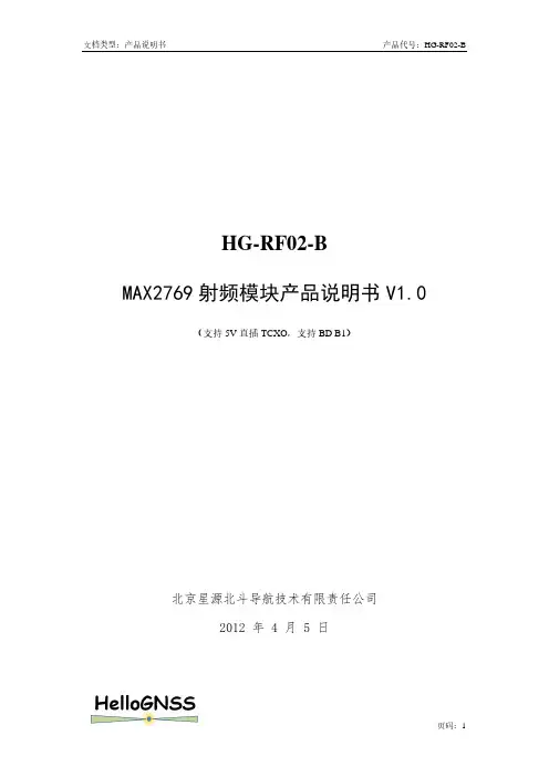
HG-RF02-BMAX2769射频模块产品说明书V1.0 (支持5V直插TCXO,支持BD B1)北京星源北斗导航技术有限责任公司2012 年 4 月 5 日Item ContextAuthor hgLast Update 2012-4-5Version 1.0Copyright(c) 北京星源北斗导航技术有限责任公司密级对外交流更多详细信息请致电星源北斗咨询!公司地址:北京市海淀区温泉镇显龙山路19号北辰香麓雅庭A座218室电话及传真:************QQ:5024141邮箱:***************1 产品简介表1 产品价格表产品价格HG-RF02-B基本组件HG-RF02-B 1000元可选配配件5米长GPS天线40元可搭配使用的其他硬件HG-RE03-B开发板(EP3C55) HG-FPGA01底板(EP3C55) 3480元2000元HG-RF02-B射频模块是在总结HG-RF02射频模块基础上设计的管脚兼容产品,模块经过HG-RE03-B接收机验证块,信号质量优异,原来HG-RF02的GPS SAW滤波器用470pF 电容替代,接收信号不受限制,适合于GPS、BD、Galieo、Glonass单系统研制。
HG-RF02-B需要外部提供3.3V和5V的电源,5V电源为射频部分供电,需要保证电源的稳定性。
2 产品特性图1 HG-RF02-B射频模块HG-RF02基本硬件如上图所示,特性如下:1.射频芯片:MAX27692.TCXO频率:16.368MHz3.默认采样率:16.368MHz4.默认中频中心频点:4.092MHz5.供电方式:3.3V和5V外接电源6.支持5V直插晶振:封装长16mm,宽8mm7.对外接口:射频输入:MMCX*2,1个有源天线输入口,1个无源天线输入口。
时钟输出:GPSCLKI支路数据:I1、I0Q支路数据:Q1、Q0SPI接口:PGM、SCLK、SDATA、nCS其他:nIDLE、nSHDN、ANTFLAG、LD、TSENS8.体积:50mm×26mm3 接口关系图2 HG-RF02-B对外接口图(符合HG-RFDIS标准)4 尺寸图图3 HG-RF02-B尺寸图(默认单位为mm)5 装箱清单1、HG-RF02-B硬件模块1块;2、配套文档:HG-RF02-B使用说明书;3、MAX2769 SPI配置参数文档:BD B1配置;6 服务条款1、半个月内如产品硬件有质量问题可免费更换;2、提供3个月QQ技术支持;3、本产品允许客户把产品提供的配置参数用于最终产品中,但不允许将本产品提供的配置参数提供给任何第三方;。
基于MAX2769的软件GPS接收机射频前端设计

基于MAX2769的软件GPS接收机射频前端设计
邵磊;刘瑞华
【期刊名称】《微型机与应用》
【年(卷),期】2010(029)016
【摘要】介绍了GPS前端的基本结构,并选用MAX2769芯片,提供了完整的中频前端放大器的参考设计.本设计的特点是接收机性能高、体积小、成本低,同时给出其USB输出的参考设计.
【总页数】4页(P30-32,36)
【作者】邵磊;刘瑞华
【作者单位】中国民航大学,航空自动化学院,天津,300300;中国民航大学,航空自动化学院,天津,300300
【正文语种】中文
【中图分类】TN965.5
【相关文献】
1.基于MAX2769的GPS软件接收机 [J], 王玉娥
2.一种五天线双频点GPS接收机射频前端设计 [J], 吴越;郑建生;刘郑
3.星载GPS接收机射频前端设计与实现 [J], 魏可友;刘成;姜泉江;刘会杰
4.GPS双频 M码接收机射频前端设计与实现 [J], 景晗;郑建生;吴越
5.GPS/Galileo卫星导航接收机射频前端设计 [J], 李党锋;李树洲;吕红丽
因版权原因,仅展示原文概要,查看原文内容请购买。
智能GPS软件接收机载波跟踪环路设计

Pk ö æC ÷ DFD =a t a n 2ç = èDPk ø θ k T) k T -T) -θ +e e( e( ω, k
) ; ) ; 叉积 PC 1 I k-1 QP( k) I k) QP( k-1) k= P( P( e DFD 的 取 值 范 围 为 ω, k 为输 入 噪 声 产 生 的 误 差 . ( ) -π, π .
Байду номын сангаас
的多普勒频移和 频 移 变 化 率 , 主要表现在载波跟 踪环路上 . 为使接收机在动态环境下 , 有较高的鲁 棒性 , 最有效的方 法 是 增 加 环 路 带 宽 和 减 少 预 积 分时间 . 然而为减 小 热 噪 声 的 影 响 和 提 高 跟 踪 精 度, 则需要减小跟踪带宽和延长预积分时间 . 目前 通过设定一个经验门限使得环路在 P L L 跟踪 , [] 和 此方法主要存在2个问 F L L P L L中切换 1 . 题: 需经常 ① 门 限 不 易 确 定; ② 若 动 态 变 化 不 定, 执行 F 跟 踪 误 差 较 大. 另 外, 文献[ 将鉴相 L L, 2]
收稿日期 : 2 0 0 6 0 3 3 0 作者简介 :唐
) 的结果直接相加进行环路 u e n c i s c r i m i n a t o r q yD 滤波 . 这一方法存在的缺陷是 , 需要较长的锁定时 ) 间, 易产生周跳 ( c c l es l i s . y p
) 器P 和鉴频器 F D( P h a s eD i s c r i m i n a t o r D( F r e -
, 斌( 男, 江苏大丰人 , 博士生 , 1 9 7 8- ) t a n b i n f r i e n d @y a h o o . c o m. c n . g
多模兼容卫星导航接收机射频前端芯片关键技术研究

结论与展望
本次演示通过对多模兼容卫星导航接收机射频前端芯片关键技术的研究,提 出了一种基于集成电路设计、频率合成、通道选择和数据传输等关键技术的解决 方案。通过实验验证,该方案在信号接收、处理和数据传输等方面均表现出良好 的性能和稳定性。
展望未来,多模兼容卫星导航接收机射频前端芯片关键技术的发展将更加注 重高集成度、低功耗、小型化和高性能等方面的优化。随着、物联网等技术的快 速发展,如何将新技术应用于多模兼容卫星导航接收机射频前端芯片的设计和优 化中,也是值得深入研究的方向。
多模兼容卫星导航接收机射频前端 芯片关键技术研究
01 引言
03 研究现状 05 实验验证
目录
02 技术概述 04 关键技术探究 06 结论与展望
引言
随着全球卫星导航系统(GNSS)的快速发展,多模兼容卫星导航接收机射频 前端芯片关键技术的研究变得越来越重要。这种技术能够在同一硬件平台上实现 多种卫星导航系统的兼容,包括全球定位系统(GPS)、格洛纳斯系统 (GLONASS)、伽利略系统(Galileo)等。多模兼容卫星导航接收机射频前端芯 片的关键技术突破,将为全球卫星导航产业的快速发展提供重要支持。
谢谢观看
实验验证
为了验证上述关键技术的有效性和可行性,我们将进行实验设计和结果验证。 首先,我们将搭建一个多模兼容卫星导航接收机射频前端芯片的测试平台,包括 信号源、频谱分析仪、示波器等测试仪器。然后,我们将对设计的射频前端芯片 进行性能测试,包括信号接收、处理和数据传输等方面的测试。通过实际测量数 据的分析,我们将评估关键技术的性能指标是否达到预期,并针对不足之处进行 优化和改进。
3、通道选择:在通道选择方面,我们将研究如何实现快速、准确的选择不 同的信号通道,以适应不同卫星导航系统的信号特性和接收需求。此外,我们还 将探究如何优化通道选择的算法和逻辑,提高通道切换的速度和稳定性。
GPS接收机射频前端电路原理与设计
GPS接收机射频前端电路原理与设计
何宇云
【期刊名称】《电脑乐园》
【年(卷),期】2021()11
【摘要】GPS 它是由美国开发的卫星导航定位系统,为全球用户提供高精度定位,
导航和定时服务。
随着GPS 技术的发展,申请领域越来越广泛地从军事领域到平民。
现在越来越多 GPS 接收器嵌入在便携式消费产品中,这项描述GPS接收器该研究
已成为具有实用价值的流行主题。
相关的测试结果表明,我们的前端电路已达到预
期的性能。
目前,前端电路已经开始应用于相关项目的设计,并且对未来的多频多系
统导航接收器的开发具有很好的参考。
【总页数】2页(P0112-0113)
【关键词】GPS接收机;双频;前端电路;原理设计
【作者】何宇云
【作者单位】广东理工学院
【正文语种】中文
【中图分类】TP
【相关文献】
1.GPS接收机射频前端电路原理与设计
2.基于SE4100L设计GPS接收机射频前
端电路3.基于NJ1006的GPS接收机射频前端电路设计4.基于GP2015射频前端电路的GPS接收机设计5.超外差结构GPS接收机射频前端电路仿真研究
因版权原因,仅展示原文概要,查看原文内容请购买。
GPS接收机射频前端电路
GPS接收机射频前端电路GPS receiver rf circuit[摘要]在GPS设计中采用了高频、低噪声放大器,以减弱天线热噪声及前面几级单元电路对接收机性能的影响;基于超外差式电路结构、镜频抑制和信道选择原理,选用芯片实现了射频单元的三级变频方案。
概述了GPS接收机基本工作原理,提出了一种基于GP2000射频前端电路的GPS接收机方案。
详细说明GP2000射频放大器的设计原理以及外围匹配电路设计方法。
重点叙述了接收机软硬件设计思路和方法。
关键词:GPS;前置放大;变频;相关器。
Abstract: In the design of high frequency used the GPS, low noise amplifier to abate antenna thermal noise and front level in the receiver unit circuit performance influence. Specialized superheterodyne type circuit based on structure, mirror frequency suppression and channel selection principle, choose chip realized the rf unit level 3 frequency conversion plan. Summarizes the basic working principle of GPS receiver, and puts forward a kind of GP2015 rf circuit based on the GPS receiver scheme. Details GP2015 rf design principle and peripheral amplifier matching circuit design method. Key described hardware and software design idea and method for the receive.Keywords: GPS,preamplifier,Frequency conversion,correlator引言:GPS(全球定位系统)以全天候、高精度、自动化、高效率等显著特点及其所独具的定位导航、授时校频、精密测量等多方面的强大功能,使其用途越来越广泛。
GPS接收机的射频前端测试原理和方法
GPS接收机的射频前端测试原理和方法作为GPS接收机重要组成部分的接收机射频前端电路是接收机动态性能的关键部件。
它的很多指标,诸如噪声系数、动态范围、镜频抑制、1dB 压缩点和相位噪声等,都直接影响接收机的性能。
因此,射频指标的准确测量对GPS 接收机性能的准确评估非常重要。
要有自主知识产权的接收机,就必须有一套完整而有效的射频模块指标的测试方法GPS信号测试的基本要求GPS 信号一般使用两个射频波段:一个信号频率为1575.42MHz(L1波段),另一个信号频率1227.6MHz(L2波段)。
一般来说,商用GPS接收机使用的波段为L1波段。
接收机接收到最小信号功耗为-133dBm到-130dBm,此信号非常微弱,淹没在噪声里。
测量 GPS 射频模块所要使用的仪器设备及配件其可用频率要高出五倍卫星信号频率以上,才能满足最基本的谐波失真测量。
对于测量中使用的同轴线、接头、负载等所有的特性阻抗都要是50Ω的特性,才能匹配良好。
同时,其辅助测试工具除了阻抗匹配良好还要具有容易校正、误差小、连接方便、高可靠性及重复性的特点。
定期校正测试仪器也很重要,而且校正时要将连接线、接头、衰减器等所有配件连接后一同测量。
GPS射频各指标测试的方法GPS 射频部分的测试方案很多,其中比较重要的指标有:增益,可控增益范围,输入压缩点,噪声系数,镜频抑制,本振到信号的隔离度,本振相噪等。
增益测量GPS 射频前端的增益是指输入到 ADC 的信号与GPS 天线接收到的信号相比的放大程度。
GPS 接收机射频前端的增益一般都在 110dB 左右。
增益可以使用频谱分析仪来测量。
低噪声放大器、混频器等器件的增益可以用向量网络分析仪来测量S21得到,注意埠的50Ω匹配。
连接如图 2。
有两个系统性能参数体现了接收机的线性度,三阶交调点和 1dB 压缩点。
三阶交调特性会将邻道信号的交调项混到有用信号中,造成信号质量的退化。
但是,对于 GPS 来说,在带内只有一个通道,没有强的邻道干扰信号,因此,主要从1dB压缩性能来考虑系统的线性度。
基于MAX2769的射频前端的设计和实现
t h e r e l a t e d p e r f o r ma n c e o f t h e s u b s e q u e n t b a s e b a n d s i g n a l p r o c e s s i n g, p l a y s a n i mp o r t a n t r o l e i n t he s a t e l l i t e n a v i g a t i o n r e c e i v e r . Th e r e f o r e , t h e c i r c u i t d e s i g n i n g s c h e me a n d i t s s p e c i f i c h a r d wa r e i mp l e me n t a t i o n o f t h e s a t e l l i t e n a v i g a t i o n r e — c e i v e r b a s e d o n M AX2 7 6 9 i s i n t r o d u c e d i n t h i s p a p e r . Th e r e l a t e d d e s i g n p a r a me t e r s o f t h e RF f r o n t — e n d a n d t h e k e y d e — s i g n t e c h n i q u e s f o r i t s RF P CB a r e a n a l y z e d i n d e t a i l . Th e t e s t r e s u l t s s h o w t h a t t h i s c i r c u i t d e s i g ni n g s c h e me i s a b l e t O s a t i s f y p r a c t i c a l r e q u i r e me n t a n d i t s c i r c u i t p e r f o r ma n c e i s o f h i g h s t a b i l i t y . Th i s s c h e me i s a p p l i c a b l e t o d e v e l o p t h e n a v i —
max2769用户手册说明书
Click here for an overview of the wireless components used in a typical radiotransceiver.Maxim > Design Support > Technical Documents > User Guides > APP 3910Keywords: GPS, receiver, GPS receiver, MAX2769, 2769, 1575MHz, Integrated GPS Receiver, Global Positioning System USER GUIDE 3910User's Guide for the MAX2769 GPS ReceiverBy: David Weber, Strategic Applications Engineer Sep 22, 2006Abstract: This note describes the MAX2769, a low-cost, single-conversion, low-IF GPS receiver chip that offers more flexibility and performance than its predecessors. Also included is a test procedure for the MAX2769 evaluation kit (EV kit) and some suggested SPI™ register settings for evaluation purposes.IntroductionThe MAX2769 is a low-cost, single-conversion, low-IF GPS receiver chip that offers more flexibility and performance than its predecessors. This device covers a wide range of GPS applications such as mobile handsets, PDAs and embedded PC, and automotiveapplications. It represents the most flexible, high-performance, low-power GPS receiver on the market.IC FeaturesLow DC Power ConsumptionPower required is typically 16mA to 23mA at 3V. Using SPI control, the device can be placed in idle mode, in which only the clock buffer and temperature sensor are active and the current consumption drops to 0.5mA.Low Associated BOM Cost and Reduced SizeThe MAX2769 is a direct down-conversion design with internal filtering that eliminates the need for external filteringcomponents. An excellent noise figure (NF) of 1.4dB for the cascaded chain (with a 0.8dB typical first-stage NF) allows this device to be used with a passive antenna. No external LNA is required. Because the design removes intermediate frequency filtering and preamplification, the MAX2769 requires less board space to implement a receiver.Flexibility for Applications Involving Active AntennasA designer can use this device with an active antenna, as in an automotive application. For an active-antenna application, a second internal path can be selected, which leads to a different LNA (LNA2) with lower gain (13dB vs. 19dB) and a slightly higher NF (1.1dB vs. 0.8dB). This approach results in a power savings of 16mA to 19mA vs. 23mA to 21mA at 3V in default mode.A voltage is provided at pin 3 specifically to bias the active device. This voltage can be turned off through the SPI interface for passive-antenna applications. If, however, the voltage is enabled, then LNA selection can be done automatically depending on whether there is an active antenna present. In the LNA-gated mode, the receiver is configured to automatically switch between the two LNAs contingent on whether a load current in excess of 1.5mA is detected at the antenna bias pin. A user does not need separate designs for applications using active and passive antennas; the chip automatically selects the appropriate LNAfor any application. If automatic LNA selection is not desired, it can be disabled through the Config1 register <14:13>.Internal Capacitive Load Trimming for Crystal ReferencesWhen using the MAX2769 with a crystal reference, no tuning of external load capacitors is required to match devices—a bank of internal crystal load capacitors can be programmed through the SPI interface to trim the load to yield the correct reference frequency. The internal bank can be programmed over a range of about 11pF to 17pF (settings plus 9pF of parasitic capacitance). A single series capacitor is placed between the crystal and the crystal/reference input. If the desired load value is between 11pF and 17pF, the value of this coupling capacitor can be made large (e.g., 10nF), so as not to affect the programmed value. For crystals with load capacitances below 11pF, the coupling capacitor can be made small to add in series with the internal bank, reducing the load seen at the device. Either way, the final frequency trimming can be done internally through the SPI interface.Reference and IF Frequency FlexibilityThe design accommodates a wide range of reference frequencies between 8MHz and 44MHz with a default setting of16.328MHz. The IF frequency is adjustable in 63 steps between 0 and 12.5MHz, with a default setting of 4.092MHz. (It is recommended that the IF frequency be kept at or below 4.092MHz, as additional steps may need to be taken to assure stability at higher frequencies.) Because of a fractional-N synthesizer that permits small step size while maintaining excellent phase noise, this flexibility does not compromise performance. No other product on the market has this degree of flexibility.IF Filter FlexibilityFiltering at IF is important as it limits the noise bandwidth and improves sensitivity while eliminating interference. TheMAX2769's IF filtering is highly flexible. The design uses a complex polyphase Butterworth configuration that can be set to 3rd or 5th order, and either bandpass or lowpass as the application dictates. The center frequency is also programmable to match the selected IF. The 3dB bandwidths can be selected as 2.5MHz, 4.2MHz, 8.0MHz, or 18MHz. Users can choose a design that optimizes performance for their application. (Note: These are two-sided 3dB bandwidths. When the lowpass option is selected, the bandwidths are cut in half and become 1.25MHz, 2.1MHz, 4.0MHz, and 9MHz. In fact, the highest setting should only be used in a lowpass configuration.) In the predecessor to this part, a 4.8MHz lowpass filter was required to pass the fixed-IF frequency data. In this design, a 2.6MHz bandpass design could be employed, thus reducing the noise bandwidth by nearly3dB and enhancing system sensitivity. Filters (in bandpass mode) are designed to have no more than 1dB droop at F C±1.023MHz.High System Gain with a Wide Range of Level ControlTo use the MAX2769 without an active antenna in a low-signal-strength environment, it is imperative that the receiver have sufficient gain. This device typically has up to 110dB available gain (in analog mode) with 60dB to 65dB of gain adjustment. Access to the Amplified RF Signal for Coexistence FilteringWhile no external filtering is required for stand-alone applications, coexistence with cellular or WiLAN transmissions in close proximity may require additional filtering to prevent overdriving the GPS receiver front-end. On the MAX2769, the RF signal has been made accessible between the first LNA stage output and mixer input (pins 2 and 5 respectively). If filtering is not desired, these ports can be connected through a coupling capacitor. However, filtering introduced at this point has minimal effect on the excellent sensitivity of the receiver. (For example, for typical device parameters, a SAW filter with 1dB insertion loss would degrade cascaded NF (and thus GPS sensitivity) by only about 0.15dB.Flexibility of Output ModesMost GPS devices provide only a single-output mode. The MAX2769's output can be programmed to be analog, CMOS, or limited differential logic in unsigned or complimentary binary format with 1- to 3-bit output from the ADC.Temperature Sensor and Status MonitoringA temperature sensor is included, which can be calibrated externally if desired. While lock-detect status can be obtained at theLD pin, the part can be programmed to instead provide the output signal, the reference clock, or results from a sigma-delta test. It can also be programmed to provide a short to the active antenna or to be an independent test point for voltage.The part is programmed through ten registers across a 3-wire SPI interface. Registers are described in Table 1. For further details, please refer to the MAX2769 data sheet.Table 1. Description of SPI Configuration RegistersCONF1<31:0>0000Configures Rx and IF sections, sets antenna bias and LNA autoselect A2919A3CONF2<31:0>0001Configures AGC and output format055028CCONF3<31:0>0010Configures PGA, and details of AGC, filtering, and data streaming EAFE1DC PLLCONFIG<31:0>0011Sets PLL, VCO, and CLK settings9EC0008DIV<31:0>0100Sets PLL main and reference division ratios0C00080FDIV<31:0>0101Sets PLL fractional division ratios8000070STRM<31:0>0110Configures DSP interface frame streaming8000000CLK<31:0>0111Sets fractional clock divider values10061B2TEST1<31:0>1000Sets up test mode1E0D401TEST2<31:0>1001Sets up test mode14C0002For initial characterization in a MAX2769 EV kit, the parameters listed in Table 2 can be measured with the suggested procedures that follow. The MAX2769 EV kit data sheet should be consulted for more details. Some settings differ from default values to facilitate testing; users are free to select different settings.Table 2. Parameters to be Tested in Suggested ProcedureLNA1 Gain27–2J7–J819dBLNA2 Gain25–2J6–J813dBSystem IP3 withLNA127–18J7–J2-26dBmSystem IP3 withLNA225–18J6–J2-20dBmLNA1 NF (DefaultMode)27–2J7–J80.8dBLNA2 NF25–2J6–J8 1.5dBLNA1 P1dB (Output)27–2J7–J88dBmLNA2 P1dB (Output)25–2J6–J810dBCascaded SystemNF, LNA127–18J7–J2 1.4dBCascaded SystemNF, LNA225–18J6–J2 2.7dBCurrentConsumption (Default Mode,11, 13, 14, 19, 23W19, W20, W11, W1219mA (default mode device only)(36mA at 3V, 140mA at ±5V for entireTEST1:1E0F401TEST2:14C0002Make sure SHDN and IDLE are set to 1, the disabled state for both.3. Measure +3V current consumption at W19 and W20.4. Input a -60dBm, 1575.42MHz CW signal at J7. Measure the signal at J8 and record the LNA1 gain. Take into account the loss on the board traces at 1575MHz around 0.35dB.5. Raise the input level until you get 1dB of compression (P1dB). (This is not a specified parameter, but you should get a number around +8dBm.) Be sure to gain correct any line losses.6. Connect a short, low-loss cable from J8 to J12 to connect the LNA1 output to the mixer. Decrease the input to -110dBm and measure the system gain by monitoring the 4.092MHz output at J2. It should be around 110dB, resulting in a 0dBm output.7. Set the maximum GAININ level by setting <3:27-22> to 63 (CONF2: 85512AC and CONF3: FEFF1DC). Decrease the input to -115dBm and measure the gain—it should be around 115dB. The input level should be adjustable through changes in GAININ. Decrease GAININ to the minimum by setting CONF3: 02FF1DC and once again measure the gain. It should be around 55dB.8. Measure IP3 using LNA1. Combine two input sources (perhaps around -55dBm input), at F1 = 1587.42MHz and F2 = 1599.42MHz (where 2 × F1 - F2 falls in-band at 1575.42MHz) and inject into J7. Measure the strength of the 4.092MHz product at J2 (Q out). Drop both inputs by 1dB, and note that the product drops by 3dB. (If not, you are compressing and need to use a lower input level.) OIP3 = (3 × P OUT - product)/2, soIIP3 = (3 × P OUT - product)/2 - gain. This reduces to (3 × (P IN + gain) - product)/2 - gain =(3 × P OUT - product + gain)/2. With a minimum (55dB) gain, P OUT = 5dBm. A typical 3rd-order product seen on the output spectrum at minimum gain might be -5dBm, in which case IIP3 = (3 × (-55) + 5 + 110)/2 = -25dBm. 9. Measure the LNA1 NF with an NF meter. The NF of the mixer stage can be measured using the gain method: by setting gain to max (see step 8), reducing the spectrum analyzer resolution bandwidth, and measuring the output S/N ratio. You need to have measured the exact system gain. For example, the input noise is -174dBm/Hz. Using an input of -100dBm and assuming around 90dB gain for the mixer stage, the receiver will not be in compression. The input S/N in a 1Hz bandwidth would be -74dB (S = 100dB/Hz, N = 174dBm/Hz). We might measure an output noise floor at J2 of -73dBm/Hz, yielding (with a -10dBm output) an SNR around 63dB. The NF of the system would then be the degradation in the S/N ratio, or 11dB. The result is approximate because measurement precision is poor. However, as the result is large and precision for this value is not critical, this approximate result is sufficient. Once again, subtract the input losses on the board (roughly 0.35dB) from all measured results. Knowing the gain of LNA1, you can then calculate cascaded NF.You could use the gain method or the y-factor method to measure the NF for the entire cascaded chain, but this result would once again be approximate.10. Return to the test register settings from step 2 and use an input level at J12 that is at least 10dB below the value that leads to 1dB compression, typically -110dB. Sweep the input frequency from 1572.9MHz to1577.9MHz to yield a passband of 2.6MHz for the IF bandpass filter. This measurement can be made by using the maximum hold option on the spectrum analyzer.11. Set up the AGC in the autonomous mode (AGC on with independent I and Q), where CONF2<12:11> = 00. Feed a signal into the LNA1 input at -150dBm and select LNA1. Note the tone power at the output while raisingthe input level to -65dBm. It should remain approximately the same (indicating AGC is working).LNA2 Tests12. Switch to LNA2 (CONF1<14:13> = 01). Input a -60dBm, 1575.42MHz CW signal at J6. Measure LNA2 gain atJ8 and record. Raise the input level until you get 1dB compression (P1dB). This is a repeat of steps 4 and 5 withLNA2. (Note again that the cascaded P1dB is determined by the mixer stage.) Cascaded gain is the linear gainmeasured here plus the gain from the mixer-in port to J2 from step 7.13. If an NF meter is available, measure the LNA2 NF between J6 and J8. Then measure the NF following theprocedure in step 9. Be sure that the AGC control is turned off so you can control the output level,CONF2<12:11> = 10.14. With default settings, measure IP3 using LNA2. Combine two sources of -55dBm input at F1 = 1587.42MHzand F2 = 1599.42MHz (where 2 × F1 - F2 falls in-band at 1575.42MHz) and inject into J6. Measure the strengthof the 4.092MHz product at J2 (Q out)—analog mode must be selected. Drop both inputs by 1dB and note thatthe product drops by 3dB. (If not, you are compressing the signal and need to use a lower input level.) CalculateIIP3 as in step 8.Digital TestsDigital measurements should be made at J9 A, B, C, and D. It has been discovered that the 74LV07 driver chip (U28) originally designed onto the board does not properly buffer these signals to allow them to be passed back to the computer on connector JDR1. To use these output signals to drive other circuitry off board, they may need to first be separately buffered.15. Change to a digital output (CONF2<5:4> = 00) so that CONF2 = 855028C, and monitor the signal on anoscilloscope. You should have a square-wave CMOS output (2.8V amplitude) at J9. With CONF2<27> = 1, both Iand Q signals should be present.Appendix: Suggested Register Settings for Initial TestCONF1: Test: A2959A3This register:Enables the chip (default)Disables the idle (default)Sets default current programmingSets non-default LO current programmingSets default mixer current programmingSelects 13MHz passive filter pole at mixer output (default)Selects LNA1 active (default; equivalent to grated mode when there is no current load on the ANT BIAS pin)Enables mixer (default)Turns off bias to external active antenna (default is bias on)Selects F C = 4.092MHzSelects 2.5MHz polyphase IF bandpass filterSelects 26dB IF filter gain (default is 17dB)CONF2: Test: 85502ACThis register:Selects both I and Q channels (default is I only)Sets AGC gain to 170 (default)Sets bit-counter length to 1024 bits (default)Selects sign/magnitude output format (default)Selects 1-bit AGC (default is 1 bit)Selects analog output driver (default is CMOS logic)Disables LO buffer (default)Enables temperature sensor (default)CONF3: Test: EAFF15CThis register:Sets the PGA gain for level/LSB at 58 (default; used only when AGC is disabled and gain is set up over SPI lines) Chooses the nominal ADC input scale (default)Selects the nominal loading for the output driver (default)Enables the ADC (default)Enables the output driver (default)Enables the filter DC-offset cancellation circuitry (default)Enables the IF filter (default)Enables AGC for both channels (default is I enabled only)Enables highpass coupling between the filter and AGC (default)Sets a 50kHz highpass pole corner frequency (default is 20kHz)Selects no DSP interface for data streaming (default)Sets the default data-counter length (16394 bits/frame)Selects 2-bit streaming (default)Enables sync pulse outputs (default)Enables frame sync pulse outputs (default)Disables data sync pulse outputs (default)Disables DSP interface reset (default)PLLCONFIG: Test: 9EC0008This register:Enables the VCO in normal current mode (default)Disables external VCO bias compensation (default)Sets clock output driver to CMOS mode (default)Sets clock frequency to XTAL frequencySelects buffer nominal current of 130mA for crystal (default; range is 130mA to 700mA)Sets capacitive load programming to 3.6pF (default; nominal for C L > 12pF)Selects PLL lock detect as output at LD pin (default)Selects nominal charge-pump operation with 0.5mA current (default)Selects 2ns charge-pump on-time selection (default)Selects integer-N PLL (default)Disables power save (default is power-save enable)Selects low-current mode for prescalar E2Cs (default is high-current mode)DIV: Test: 0C00080This register:Sets N = 1536 for low-side injection (default; LO = 1536 × 1.023MHz = 1571.328MHz)Sets R = 16 (default; step size = 16.368MHz/16 = 1.023MHz)FDIV: Test: 8000070This register:Sets fractional division ratio = 80000 (default)Selects nominal current and filter trim valuesSTRM: Test: 8000000This register:Sets nominal stream interface control to start at a frame given by FRAME_COUNTCLK: Test: 10061B2This register:Sets the L counter to 256Sets the M counter to 1563Selects a fractional clock input to the fractional clock divider to come after the reference divider Selects the serializer clock to come from the reference divider(When integer-N is selected in the PLL Config register, these settings are not used.)TEST1: Test: 1E0F401This register is reserved for TestTEST2: Test: 14C0002This register is reserved for TestThe screen format for setting configurations is shown in Figure 1.Figure 1. The MAX2769 EV kit test software screen format shows suggested settings.Related PartsMAX2769Universal GPS Receiver Free SamplesFree Samples MAX4444Ultra-High-Speed, Low-Distortion, Differential-to-Single-Ended LineReceivers with EnableMore InformationFor Technical Support: /supportFor Samples: /samplesOther Questions and Comments: /contactApplication Note 3910: /an3910USER GUIDE 3910, AN3910, AN 3910, APP3910, Appnote3910, Appnote 3910 Copyright © by Maxim Integrated ProductsAdditional Legal Notices: /legal。