S-809XXC中文资料
S-80950中文资料

Features
• Ultra-low current consumption 1.0 µA typ. (VDD=2.0 V) ; Products with a detection voltage of 1.4V or less 1.2 µA typ. (VDD=3.5 V) ; Products with a detection voltage of 1.5V or more • High-precision detection voltage ±2.0% • Low operating voltage 0.80 to 6.0 V ; Products with detection voltage of 1.4‚uor less
SOT-23-5 Top view
5 4 1 OUT 2 VDD 3 VSS 4 NC 1 2 3 5 CD
Pin Assignment
Figure 1
Block Diagram
(1) Nch open-drain active low output (2) CMOS active low output
Table 1
Detection voltage range (V) 1.1V±2.0% 1.2V±2.0% 1.3V±2.0% 1.4V±2.0% 1.5V±2.0% 1.6V±2.0% 1.7V±2.0% 1.8V±2.0% 1.9V±2.0% 2.0V±2.0% 2.1V±2.0% 2.2V±2.0% 2.3V±2.0% 2.4V±2.0% 2.5V±2.0% 2.6V±2.0% 2.7V±2.0% 2.8V±2.0% 2.9V±2.0% 3.0V±2.0% 3.1V±2.0% 3.2V±2.0% 3.3V±2.0% 3.4V±2.0% 3.5V±2.0% 3.6V±2.0% 3.7V±2.0% 3.8V±2.0% 3.9V±2.0% 4.0V±2.0% 4.1V±2.0% 4.2V±2.0% 4.3V±2.0% 4.4V±2.0% 4.5V±2.0% 4.6V±2.0% 4.7V±2.0% 4.8V±2.0% 4.9V±2.0% 5.0V±2.0% 5.1V±2.0% 5.2V±2.0% 5.3V±2.0% 5.4V±2.0% 5.5V±2.0% 5.6V±2.0% 5.7V±2.0% 5.8V±2.0% 5.9V±2.0% 6.0V±2.0% Hysteresis width VHYS typ.(V) 0.055 0.060 0.065 0.070 0.075 0.080 0.085 0.090 0.095 0.100 0.105 0.110 0.115 0.120 0.125 0.130 0.135 0.140 0.145 0.150 0.155 0.160 0.165 0.170 0.175 0.180 0.185 0.190 0.195 0.200 0.205 0.210 0.215 0.220 0.225 0.230 0.235 0.240 0.245 0.250 0.255 0.260 0.265 0.270 0.275 0.280 0.285 0.290 0.295 0.300 Nch Open Drain(Low) S-80911ANMP-D71-T2 S-80912ANMP-D72-T2 S-80913ANMP-DDA-T2 S-80914ANMP-DDB-T2 S-80915ANMP-DDC-T2 S-80916ANMP-DDD-T2 S-80917ANMP-DDE-T2 S-80918ANMP-DDF-T2 S-80919ANMP-DDG-T2 S-80920ANMP-DDH-T2 S-80921ANMP-DDJ-T2 S-80922ANMP-DDK-T2 S-80923ANMP-DDL-T2 S-80924ANMP-DDM-T2 S-80925ANMP-DDN-T2 S-80926ANMP-DDP-T2 S-80927ANMP-DDQ-T2 S-80928ANMP-DDR-T2 S-80929ANMP-DDS-T2 S-80930ANMP-DDT-T2 S-80931ANMP-DDV-T2 S-80932ANMP-DDW-T2 S-80933ANMP-DDX-T2 S-80934ANMP-DDY-T2 S-80935ANMP-DDZ-T2 S-80936ANMP-DD0-T2 S-80937ANMP-DD1-T2 S-80938ANMP-DD2-T2 S-80939ANMP-DD3-T2 S-80940ANMP-DD4-T2 S-80941ANMP-DD5-T2 S-80942ANMP-DD6-T2 S-80943ANMP-DD7-T2 S-80944ANMP-DD8-T2 S-80945ANMP-DD9-T2 S-80946ANMP-DJA-T2 S-80947ANMP-DJB-T2 S-80948ANMP-DJC-T2 S-80949ANMP-DJD-T2 S-80950ANMP-DJE-T2 S-80951ANMP-DJF-T2 S-80952ANMP-DJG-T2 S-80953ANMP-DJH-T2 S-80954ANMP-DJJ-T2 S-80955ANMP-DJK-T2 S-80956ANMP-DJL-T2 S-80957ANMP-DJM-T2 S-80958ANMP-DJN-T2 S-80959ANMP-DJP-T2 S-80960ANMP-DJQ-T2 CMOS Output(Low) S-80911ALMP-D51-T2 S-80912ALMP-D52-T2 S-80913ALMP-DAA-T2 S-80914ALMP-DAB-T2 S-80915ALMP-DAC-T2 S-80916ALMP-DAD-T2 S-80917ALMP-DAE-T2 S-80918ALMP-DAF-T2 S-80919ALMP-DAG-T2 S-80920ALMP-DAH-T2 S-80921ALMP-DAJ-T2 S-80922ALMP-DAK-T2 S-80923ALMP-DAL-T2 S-80924ALMP-DAM-T2 S-80925ALMP-DAN-T2 S-80926ALMP-DAP-T2 S-80927ALMP-DAQ-T2 S-80928ALMP-DAR-T2 S-80929ALMP-DAS-T2 S-80930ALMP-DAT-T2 S-80931ALMP-DAV-T2 S-80932ALMP-DAW-T2 S-80933ALMP-DAX-T2 S-80934ALMP-DAY-T2 S-80935ALMP-DAZ-T2 S-80936ALMP-DA0-T2 S-80937ALMP-DA1-T2 S-80938ALMP-DA2-T2 S-80939ALMP-DA3-T2 S-80940ALMP-DA4-T2 S-80941ALMP-DA5-T2 S-80942ALMP-DA6-T2 S-80943ALMP-DA7-T2 S-80944ALMP-DA8-T2 S-80945ALMP-DA9-T2 S-80946ALMP-DEA-T2 S-80947ALMP-DEB-T2 S-80948ALMP-DEC-T2 S-80949ALMP-DED-T2 S-80950ALMP-DEE-T2 S-80951ALMP-DEF-T2 S-80952ALMP-DEG-T2 S-80953ALMP-DEH-T2 S-80954ALMP-DEJ-T2 S-80955ALMP-DEK-T2 S-80956ALMP-DEL-T2 S-80957ALMP-DEM-T2 S-80958ALMP-DEN-T2 S-80959ALMP-DEP-T2 S-80960ALMP-DEQ-T2
RE John (XXXXXX) XXXXXXX, Age 18, DOB XXXX1986

Sample Letter to Document Disability From Primary Care PhysicianTo Vocational RehabilitationDateTO: NAME OF VR COUNSELOROffice of Rehabilitation ServicesADDRESSCITY, STATEFROM: DOCTOR’s NAME (its better if this is on the physician’s letterhead)RE: John (XXXXXX) XXXXXXX, Age 18, DOB XX/XX/1986Phone: XXX-XXX-XXXXGraduate of XXXXXX High School as of June 9, 2004Dear NAME OF VR COUNSELOR,The purpose of this letter is to document significant chronic health conditions that impair activities of daily living for XXXXXXX – XXXXXX. I have been his primary care physician for18 years.XXXXXX’s health issues and their effect on school and potential employment do meet the definition of disability by Utah’s Vocational Rehabilitation criteria [Title 53A Chapter 24, 102(3)] and ADA and Section 504 requirements (see fact sheet on last page).SIGNIFICANT HEALTH IMPAIRMENTS• Endocrine System - TYPE ONE DIABETES• Digestive System - ULCERATIVE COLITIS• Immune System - ANKYLOSING SPONDYLITISCONFIDENTIALITY SAFEGUARDS - In compliance with HIPAA confidentiality mandates permission for this personal health information has been obtained by the patient, and as such this letter should be treated as highly confidential records and not shared without the patient’s permission.What follows is an overview of the health issues that XXXXXX lives with. Enclosed are relevant reports and findings of recent and past health related medical testing.TRAINING FOR EMPLOYMENT & IMPORTANT OF HEALTH CARE BENEFITSIt is important to consider what XXXXXX could do to meet his potential, live independently, and remain as healthy as possible. XXXXXX is a very bright young man who has displayed numerous talents in music, art, writing, literature, and science.Given his educational performance, intellectual abilities and aspirations, he certainly has the potential to do well in competitive employment through post-secondary college courses – if supported. It will be essential that career development be aimed at stable; well-paying jobs that offer comprehensive benefits to assure maintain health status and financial independence.In sum, I believe that offering XXXXXX financial and technology support through the Office of Rehabilitative Services would ensure not only employability but also would support all important aspects of independent living and optimal quality of life. Please contact me if you require further information.Sincerely,XXXXXXXXX, M.D.Etc.XXXXXX XXXXXX Chronic Health Issues1. TYPE ONE DIABETES, ICD-9 CODE: 250.01, Diagnosed: 1998; age 12 yearsHealth Impact to XXXXXX – He requires daily insulin, strict dietary management, and daily/hourlymonitoring and management of blood sugar levels. He has been hospitalized several times, either forsevere hypoglycemia or ketoacidosis.2. ULCERATIVE COLITIS, ICD-9 CODE: 556.9, Diagnosed: Diagnosed 2000; age 14 yearsXXXXXX required surgery for this. He had a colectomy.Health Impact to XXXXXX – Although he technically no longer has ulcerative colitis due to the absence of a colon, he continues to suffer from acute episodes of pouchitis. Symptoms, including steadily increasingstool frequency that may be accompanied by incontinence, bleeding, fever and/or feeling of urgency. Most cases can be treated with a short course of antibiotics. Additionally, absence of a colon causes problemswith nutritional absorption and is associated with XXXXXX’s below-average weight.3. ANKYLOSING SPONDYLITIS, ICD-9 CODE: 720.0, Diagnosed: 2000; age 14 yearsHealth Impact to XXXXXX – his degenerative spinal arthritis that causes episodes of severe pain andlimitations on his physical capabilities, requiring medication and a physical therapy regime formanagement.ACCOMODATIONS REQUIRED – SCHOOL /EMPLOYMENT TRAINING/PREPARATIONIn order to maximize XXXXXX’s performance level that will not jeopardize health status, some accommodations and modifications are required:1. DAILY MONITORING- XXXXXX’s diabetes management requires that he be able to take frequent breaks whenthe need arises to a) treat low blood sugars, b) use the restroom, c) test his glucose levels, and d) administer insulin. Although XXXXXX’s diabetes management has been relatively stable, the presence of additionalautoimmune diseases puts his future diabetes management and long-term health at risk.2. WATER INTAKE & BATHROOM BREAKS - XXXXXX’s lack of a colon causes him to use the restroom frequently,and he must drink a large amount of water throughout the day to prevent dehydration.3. LIMIT PHYSICAL EXERTION - His ankylosing spondylitis causes him days with severe back pain, makingrigorous activity very painful. Tasks requiring heavy lifting or having to sit or stand for a prolonged period of time without breaks exacerbate his condition and are harmful to his spine. Class schedules and location of classrooms, time needed to change travel to next class need to be evaluated. There may be a need foradditional accommodations in the future, such as mobility assistance, elevator use, use of laptop or cell phone to alleviate unnecessary physical travel.4. ATTENDANCE - Episodes of severe hypoglycemia or ketoacidosis, pouchitis infections, and severe spinal paincan result in XXXXXX’s need for additional sick days to treat the accompanying fever, diarrhea, and abdominal pain. Teachers will need to allow for increased time to make up schoolwork or other forms of instruction if absenteeism is due to noted health issues.5. ACCOMODATIONS - XXXXXX has had a 504 plan in place at school (K-12) to ensure these accommodationshave been allowed. The individualized employment plan / individual written rehabilitation plan, that will be developed between VR and XXXXXX will need to specify needed accommodations. While in college, XXXXXX will need to coordinate accommodations (health, learning and testing) for maximized performance with the Disability Resource Centers on campus.。
MAX809S中文资料
19-0344; Rev 5; 1/01
3-Pin Microprocessor Reset Circuits
General Description
The MAX803/MAX809/MAX810 are microprocessor (µP) supervisory circuits used to monitor the power supplies in µP and digital systems. They provide excellent circuit reliability and low cost by eliminating external components and adjustments when used with +5V, +3.3V, +3.0V, or +2.5V powered circuits. These circuits perform a single function: they assert a reset signal whenever the VCC supply voltage declines below a preset threshold, keeping it asserted for at least 140ms after VCC has risen above the reset threshold. Reset thresholds suitable for operation with a variety of supply voltages are available. The MAX803 has an open-drain output stage, while the MAX809/MAX810 have push-pull outputs. The MAX803’s open-drain RESET output requires a pull-up resistor that can be connected to a voltage higher than VCC. The MAX803/MAX809 have an active-low RESET output, while the MAX810 has an active-high RESET output. The reset comparator is designed to ignore fast transients on VCC, and the outputs are guaranteed to be in the correct logic state for VCC down to 1V. Low supply current makes the MAX803/MAX809/ MAX810 ideal for use in portable equipment. The MAX803 is available in a 3-pin SC70 package, and the MAX809/MAX810 are available in 3-pin SC70 or SOT23 packages.
MAX809SD中文资料
COVER TAPECARRIER TAPEREELAS-SEMBLY TAPE GUARBAND CODELABELBOXFigure 8. Tape and reel packing method.MAX809/MAX810 3-pin microprocessor resetsSOT23-3: plastic small outline package; 3 leads; body width 1.5 mm1.351.21.00.250.500.250.220.083.002.701.701.500.550.352310.150.0510°0°MAX809/MAX810 3-pin microprocessor resetsSC70-3:plastic small outline package; 3 leads; body width 1.15 mm1.0 0.80.40.250.2250.102.11.90.40.1MAX809/MAX810 3-pin microprocessor resetsDefinitionsShort-form specification — The data in a short-form specification is extracted from a full data sheet with the same type number and title. For detailed information see the relevant data sheet or data handbook.Limiting values definition — Limiting values given are in accordance with the Absolute Maximum Rating System (IEC 60134). Stress above one or more of the limiting values may cause permanent damage to the device. These are stress ratings only and operation of the device at these or at any other conditions above those given in the Characteristics sections of the specification is not implied. Exposure to limiting values for extended periods may affect device reliability.Application information — Applications that are described herein for any of these products are for illustrative purposes only. Philips Semiconductors make no representation or warranty that such applications will be suitable for the specified use without further testing or modification.DisclaimersLife support — These products are not designed for use in life support appliances, devices, or systems where malfunction of these products can reasonably be expected to result in personal injury. Philips Semiconductors customers using or selling these products for use in such applications do so at their own risk and agree to fully indemnify Philips Semiconductors for any damages resulting from such application.Right to make changes — Philips Semiconductors reserves the right to make changes in the products—including circuits, standard cells, and/or software—described or contained herein in order to improve design and/or performance. When the product is in full production (status ‘Production’), relevant changes will be communicated via a Customer Product/Process Change Notification (CPCN). Philips Semiconductors assumes no responsibility or liability for the use of any of these products, conveys no license or title under any patent, copyright, or mask work right to these products, and makes no representations or warranties that these products are free from patent, copyright, or mask work right infringement, unless otherwise specified.Contact informationFor additional information please visit.Fax: +31 40 27 24825For sales offices addresses send e-mail to:© Koninklijke Philips Electronics N.V. 2003All rights reserved. Printed in U.S.A.Date of release: 08-03Document order number:9397 750 11889。
2Bxxxx-xxx-3BD中文资料
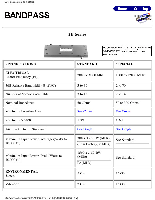
2B SeriesSPECIFICATIONS STANDARD *SPECIAL ELECTRICALCenter Frequency (Fc)2000 to 9000 Mhz 1000 to 12000 MHz 3dB Relative Bandwidth (% of FC) 3 to 30 2 to 70Number of Sections Available 3 to 10 2 to 14Nominal Impedance 50 Ohms 50 to 300 Ohms Maximum Insertion Loss See Curve See Curve Maximum VSWR 1.5/1 1.3/1Attenuation in the StopbandSee GraphSee Graph Maximum Input Power (Average)(Watts to 10,000 ft.)300 x 3 db BW (MHz)(Loss Factor)(Fc MHz)See StandardMaximum Input Power (Peak)(Watts to 10,000 ft.)1500 x 3 dB BW (MHz)Fc (MHz)See StandardENVIRONMENTAL Shock 5 G's 15 G's Vibration2 G's15 G'sHumidity90% relative100% relative Altitude Unlimited UnlimitedTemperature Range (Operating)-25 to + 50 degreescelsius-54 to + 100 degreescelsiusTemperature Range (Non-Operating)-54 to + 70 degreescelsius-62 to +150 degreescelsiusMECHANICALApproximate Weight in oz.1.7 x L x W 1.0 x L x WMounting Provisions See below Consult FactoryINSERTION LOSS:The Maximum Insertion Loss atcenter frequency is equal to :LF x (N + 0.5) / % 3 dB BW + 0.1Where:LF= Loss Factor, N= Number ofSections% 3dB BW:3dB BW (MHz) x 100divided byCenter Frequency (MHz)Example:A 5 section 2B with a centerfrequencey of 5000 MHz and a 3dBBW of 500 MHz would have,.08 x 5.5 /10 = 4.4 /10 = 0.44 + 0.1= 0.5 dbMECHANICAL SPECIFICATIONSL Dimension = 1.5 inch = (0.5 x No. of Sections) Approx.W Dimension = 2950 / Fc (MHz) + 0.6 inch Approx.Connectors Available On 2B Series:Lark Code Type C DIM.Inches & MM Lark Code Type C DIM.Inches & MM A SMA JACK .375 & 9.5*G N JACK .736 & 18.7BSMA PLUG.507 & 12.9*HN PLUG.819 & 20.8Lark Engineering SD SERIES元器件交易网*C TNC JACK .750 & 19.1S SPECIAL*D TNC PLUG.844 & 21.4* Not recommended for use with this SeriesThe size shown is a standard used by Lark to facilitate a low cost, easily reproducible unit. Should you require another size, please submit all of your requirements-both electrical and mechanical. This will enable Lark Engineering to quote theoptimum design for your application.Lark Engineering SD SERIES元器件交易网STOPBAND SPECIFICATIONSThe graphs on the following pages define the normal specification limits on attenuation Lark bandpass filter series 2B, 3B, and 4B. The minimum level of attenuation in dB is shown as a "number of 3dB bandwidths from centerfrequency".Since the frequency characteristics vary for differing bandwidths, it is necessary to establish specifications for each bandwidth of filter. The different graphs represent various 3dB percentage bandwidths. Intermediate values should be interpolated. The 3dB percentage bandwidth is defined as follows:3dB Bandwidth (MHz) x 100divided byCenter Frequency (MHz)The exact relationship is as follows:1. 3dB Bandwidths From Center Frequency= Rejection Frequency (Mhz) -Center Frequency (Mhz) divided by 3dB Bandwidth (Mhz)Example:Given:2. Center Frequency = 5000 MHz Minimum 3dB Bandwidth = 500 MHzNumber of Sections = 5Find: Minimum attenuation levels at 4250 MHz and 5800 MHz.3dB BW's from Fc = 4250 - 5000 / 500 = - 1.5and 5800 - 5000 / 500 = + 1.6The answer can be read directly from the 10% graph. Using the 5 section curve at the point -1.5 (4250 MHz) we find the minimum level of attenuation is 40dB.At +1.6 (5800 MHz) the minimum level of attenuation is 50dB.For special requirements, please contact our Application EngineeringDepartment.STOPSP3.HTM元器件交易网STOPBAND SPECIFICATIONSSTOPBAND SPECIFICATIONSSTOPSP3.HTM元器件交易网STOPBAND SPECIFICATIONS。
809协议解析

809协议解析摘要:一、809协议简介1.背景与起源2.主要特点二、809协议解析1.协议结构2.关键参数解读3.应用场景三、809协议在我国的实施与应用1.标准化进程2.行业应用案例四、809协议的优缺点分析1.优点2.缺点五、展望809协议的未来发展1.技术迭代与升级2.潜在挑战与应对策略正文:一、809协议简介1.背景与起源809协议,全称为“工业自动化系统与集成协议”,起源于20世纪80年代末,由美国仪表制造商协会(ISA)主导制定。
其目的是为了解决工业自动化领域设备与系统之间的通信问题,推动自动化技术的进步与发展。
2.主要特点809协议具有以下特点:(1)面向对象:以设备或系统功能为单位进行通信,实现设备间的互操作性。
(2)信息模型:定义了设备或系统功能所需的数据结构、数据类型和数据传输方式。
(3)协议分层:遵循ISO/OSI七层模型,实现不同层次设备之间的通信。
(4)可扩展性:支持子协议和扩展,可根据实际应用需求进行定制。
二、809协议解析1.协议结构809协议主要包括以下几个部分:(1)物理层:定义了通信介质的物理和电气特性,如电缆、波特率等。
(2)数据链路层:实现错误检测、流量控制和数据帧的传输,采用问答式通信。
(3)网络层:负责设备之间的寻址和路由,实现数据包的传输。
(4)传输层:提供可靠或不可靠的数据传输服务,实现设备间的数据交换。
(5)会话层:建立、管理和终止设备之间的会话。
(6)表示层:处理数据表示、编码和解码等问题。
(7)应用层:提供设备或系统功能的通信服务。
2.关键参数解读(1)设备地址:唯一标识一个设备,用于网络层和传输层通信。
(2)数据类型:定义了数据传输时使用的数据类型,如整型、浮点型等。
(3)传输速率:数据链路层和物理层之间的通信速率。
(4)错误检测:采用奇偶校验、循环冗余校验等方法实现数据传输过程中的错误检测。
3.应用场景809协议主要应用于工业自动化领域,如生产线控制系统、楼宇自控系统等,实现设备间的高效、可靠通信。
HQxxxx-xxx-3AA中文资料

HQ SeriesSPECIFICATIONS STANDARD*SPECIAL ELECTRICALCenter Frequency (Fc)100 to 1000 Mhz80 to 1400 MHz 3dB Relative Bandwidth (% of FC) 4 to 40 4 to 50 Number of Sections Available 3 to 8 2 to 10 Nominal Impedance50 Ohms50 to 75 Ohms Maximum Insertion Loss See Curve See Curve Maximum VSWR 1.5/1 1.3/1 Attenuation in the Stopband See Graph See GraphMaximum Input Power (Average)(Watts to10,000 ft.)500 x 3dB BW (MHz)(Loss Factor)(Fc MHz)See StandardMaximum Input Power (Peak)(Watts to10,000 ft.)300 x 3dB BW (MHz)Fc (MHz)2,000ENVIRONMENTALShock15 G's25 G's Vibration 5 G's10 G's Humidity90% relative100% relativeINSERTION LOSS:The Maximum Insertion Loss at center frequency is equal to :LF x (N + 0.5) / % 3 dB BW + 0.2 Where:LF= Loss Factor, N= Number of Sections% 3dB BW:3dB BW (MHz) x 100divided byCenter Frequency (MHz) Example:A 3 section HQ with a center frequency of 400 MHz and a 3dB BW of 40 MHz would have,1.5 x 3.5 / 10 = 5.25 / 10 = 0.525 0.525 + 0.2 = 0.8 dBConnectors Available on HQ Series:Lark Code Type C DIM.Inches & MMLarkCodeType C DIM.Inches & MMA SMA JACK.800 & 20.3G N JACK 1.625 & 41.3B SMA PLUG.855 & 22.5H N PLUG 1.585 & 40.3C TNC JACK 1.350 & 34.3L SOLDER MPINAXIAL.625 & 15.9D TNC PLUG 1.280 & 32.5*M SOLDER PINRADIAL.625 & 15.9E BNC JACK 1.350 & 34.3S SPECIALF BNC PLUG 1.280 & 32.5*Not recommended for use with this series.LENGTH:The approximate length of a Lark HQ series filter can be determined by the formula:( 0.5 N + 2 / %BW ) x LC = LWhere N is the number of sections used, % BW is:3dB BW (MHz) x 100divided byCENTER FREQUENCY (MHz)LC is the length constant at the specified center frequency, L is the dimension between theconnectors; C1 and C2 are the connector lengths as shown above. All of the length information given here is approximate. Exact length specifications must be quoted by the factory. If a special length is needed,please submit all of your requirements - both electrical and mechanical. This will enable Lark Engineering to quote the optimum design for your application.Example:A 3 section HQ with a center frequency of 400 MHz a 3dB BW of 40 MHz and SMA jack input and output connectors would be:(1.5 + 0.2) x 1.38 = 2.35 + C1 + C2In most cases, the L dimension is rounded to the nearest 1/4 inch which in this instance would be 2.25inches and the O.A.L. is:2.25 + .800 + .800 =3.85 inches.To convert inches to millimeters multiply x 25.40.Lark Engineering HQ SERIES元器件交易网STOPBAND ATTENUATIONThe graph on the following pages defines the normal specification limits on attenuation Lark bandpass filter series HP, HQ, SF, and SM. The minimum level of attenuation in dB is shown as a "number of 3dB bandwidths from center frequency".Since the frequency characteristics vary for differing bandwidths, it is necessary to establishspecifications for each bandwidth of filter. The different graphs represent various 3dB percentage bandwidths. Intermediate values should be interpolated. The 3dB percentage bandwidth is defined asfollows:STOPATT5.HTM元器件交易网As the 3dB bandwidth is exactly 10% of the center frequency, the answer can be read directly from the 10% graph. Using the 5 section curve at the point -1.5 (255 MHz) we find the minimum level of attenuation is 36dB. At +1.6 (348 MHz) the minimum level of attenuation is 48dB.For special requirements, please contact our Application Engineering Department.STOPBAND ATTENUATIONSTOPBAND ATTENUATIONSTOPATT5.HTM元器件交易网STOPBAND ATTENUATIONSTOPBAND ATTENUATIONSTOPBAND ATTENUATION。
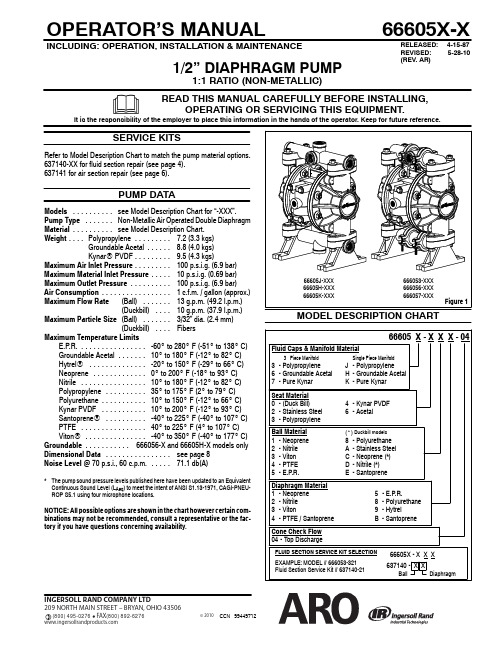
66605X-XXX-EN
WARNING STATIC SPARK. Can cause explosion resulting in severe injury or death. Ground pump and pumping system.
(800) 495-0276 FAX(800) 892-6276
© 2010 CCN 99449712
OPERATING AND SAFETY PRECAUTIONS
READ, UNDERSTAND AND FOLLOW THIS INFORMATION TO AVOID INJURY AND PROPERTY DAMAGE.
E.P.R. . . . . . . . . . . . . . . . . -60_ to 280_ F (-51_ to 138_ C) Groundable Acetal . . . . . . . 10_ to 180_ F (-12_ to 82_ C) HytrelR . . . . . . . . . . . . . . -20_ to 150_ F (-29_ to 66_ C) Neoprene . . . . . . . . . . . . . 0_ to 200_ F (-18_ to 93_ C) Nitrile . . . . . . . . . . . . . . . . 10_ to 180_ F (-12_ to 82_ C) Polypropylene . . . . . . . . . . 35_ to 175_ F (2_ to 79_ C) Polyurethane . . . . . . . . . . . 10_ to 150_ F (-12_ to 66_ C) Kynar PVDF . . . . . . . . . . . 10_ to 200_ F (-12_ to 93_ C) SantopreneR . . . . . . . . . . -40_ to 225_ F (-40_ to 107_ C) PTFE . . . . . . . . . . . . . . . . 40_ to 225_ F (4_ to 107_ C) VitonR . . . . . . . . . . . . . . . -40_ to 350_ F (-40_ to 177_ C) Groundable . . . . . . . . . . . 666056-X and 66605H-X models only Dimensional Data . . . . . . . . . . . . . . . . see page 8 Noise Level @ 70 p.s.i., 60 c.p.m. . . . . . 71.1 db(A)
- 1、下载文档前请自行甄别文档内容的完整性,平台不提供额外的编辑、内容补充、找答案等附加服务。
- 2、"仅部分预览"的文档,不可在线预览部分如存在完整性等问题,可反馈申请退款(可完整预览的文档不适用该条件!)。
- 3、如文档侵犯您的权益,请联系客服反馈,我们会尽快为您处理(人工客服工作时间:9:00-18:30)。
Rev.3.3_00ULTRA-SMALL PACKAGE HIGH-PRECISION VOLTAGE DETECTORS-809xxC SeriesWITH DELAY CIRCUIT (EXTERNAL DELAY TIME SETTING)The S-809xxC Series is a high-precision voltagedetector developed using CMOS process. Thedetection voltage is fixed internally with an accuracy of±2.0 %. A time delayed reset can be accomplishedwith the addition of an external capacitor. Two outputforms, Nch open-drain and CMOS output, areavailable.Features• Ultra-low current consumption 1.0 μA typ. (Detection voltage ≤ 1.4 V, at V DD=2.0 V)μA typ. (Detection voltage ≥ 1.5 V, at V DD=3.5 V)1.1• High-precision detection voltage ±2.0 %• Operating voltage range 0.7 V to 10.0 V• Hysteresis characteristics 5 % typ.• Detection voltage 1.3 V to 6.0 V (0.1 V step)• Output forms Nch open-drain output (Active Low)CMOS output (Active Low)• Lead-free productsApplications• Power supply monitor for portable equipment such as notebook PCs, digital still cameras, PDAs and cellular phones• Constant voltage power monitor for cameras, video equipment and communication equipment• Power monitor and reset for CPUs and microcomputersPackagesPackage name Drawing codeLandReelTapePackageNP004-A—NP004-ASC-82AB NP004-AMP005-A—MP005-ASOT-23-5 MP005-ASNT-4A PF004-A PF004-A PF004-A PF004-AS-809xxC SeriesRev.3.3_00Block Diagrams1. Nch Open-drain Output ProductsVSSVDDOUT CD*1. Parasitic diodeFigure 12. CMOS Output ProductsOUTCD*1. Parasitic diodeFigure 2Rev.3.3_00S-809xxC SeriesProduct Name StructureThe detection voltage, output form and packages for S-809xxC Series can be selected at the user's request. Refer to the "1. Product Name" for the construction of the product name and "2. Product Name List" for the full product names.1. Product NameS -*1.*2. Refer to the Table 1 to 2 in the “2. Product Name List”S-809xxC Series Rev.3.3_002. Product Name List2-1. Nch Open-drain Output ProductsTable 1Detection voltagerange Hysteresiswidth (Typ.)SC-82AB SOT-23-5 SNT-4A1.3 V ±2.0 % 0.065 V S-80913CNNB-G8HT2G S-80913CNMC-G8HT2G S-80913CNPF-G8HTFG 1.4 V ±2.0 % 0.070 V S-80914CNNB-G8JT2G S-80914CNMC-G8JT2G S-80914CNPF-G8JTFG 1.5 V ±2.0 % 0.075 V S-80915CNNB-G8KT2G S-80915CNMC-G8KT2G S-80915CNPF-G8KTFG 1.6 V ±2.0 % 0.080 V S-80916CNNB-G8LT2G S-80916CNMC-G8LT2G S-80916CNPF-G8LTFG 1.7 V ±2.0 % 0.085 V S-80917CNNB-G8MT2G S-80917CNMC-G8MT2G S-80917CNPF-G8MTFG 1.8 V ±2.0 % 0.090 V S-80918CNNB-G8NT2G S-80918CNMC-G8NT2G S-80918CNPF-G8NTFG1.9 V ±2.0 % 0.095 V S-80919CNNB-G8PT2G S-80919CNMC-G8PT2G S-80919CNPF-G8PTFG2.0 V ±2.0 % 0.100 V S-80920CNNB-G8QT2G S-80920CNMC-G8QT2G S-80920CNPF-G8QTFG 2.1 V ±2.0 % 0.105 V S-80921CNNB-G8RT2G S-80921CNMC-G8RT2G S-80921CNPF-G8RTFG 2.2 V ±2.0 % 0.110 V S-80922CNNB-G8ST2G S-80922CNMC-G8ST2G S-80922CNPF-G8STFG 2.3 V ±2.0 % 0.115 V S-80923CNNB-G8TT2G S-80923CNMC-G8TT2G S-80923CNPF-G8TTFG 2.4 V ±2.0 % 0.120 V S-80924CNNB-G8UT2G S-80924CNMC-G8UT2G S-80924CNPF-G8UTFG 2.5 V ±2.0 % 0.125 V S-80925CNNB-G8VT2G S-80925CNMC-G8VT2G S-80925CNPF-G8VTFG 2.6 V ±2.0 % 0.130 V S-80926CNNB-G8WT2G S-80926CNMC-G8WT2G S-80926CNPF-G8WTFG 2.7 V ±2.0 %0.135 V S-80927CNNB-G8XT2G S-80927CNMC-G8XT2G S-80927CNPF-G8XTFG 2.8 V ±2.0 % 0.140 V S-80928CNNB-G8YT2G S-80928CNMC-G8YT2G S-80928CNPF-G8YTFG2.9 V ±2.0 % 0.145 V S-80929CNNB-G8ZT2G S-80929CNMC-G8ZT2G S-80929CNPF-G8ZTFG3.0 V ±2.0 % 0.150 V S-80930CNNB-G80T2G S-80930CNMC-G80T2G S-80930CNPF-G80TFG 3.1 V ±2.0 % 0.155 V S-80931CNNB-G81T2G S-80931CNMC-G81T2G S-80931CNPF-G81TFG 3.2 V ±2.0 % 0.160 V S-80932CNNB-G82T2G S-80932CNMC-G82T2G S-80932CNPF-G82TFG 3.3 V ±2.0 % 0.165 V S-80933CNNB-G83T2G S-80933CNMC-G83T2G S-80933CNPF-G83TFG 3.4 V ±2.0 % 0.170 V S-80934CNNB-G84T2G S-80934CNMC-G84T2G S-80934CNPF-G84TFG 3.5 V ±2.0 % 0.175 V S-80935CNNB-G85T2G S-80935CNMC-G85T2G S-80935CNPF-G85TFG 3.6 V ±2.0 % 0.180 V S-80936CNNB-G86T2G S-80936CNMC-G86T2G S-80936CNPF-G86TFG 3.7 V ±2.0 % 0.185 V S-80937CNNB-G87T2G S-80937CNMC-G87T2G S-80937CNPF-G87TFG 3.8 V ±2.0 % 0.190 V S-80938CNNB-G88T2G S-80938CNMC-G88T2G S-80938CNPF-G88TFG3.9 V ±2.0 % 0.195 V S-80939CNNB-G89T2G S-80939CNMC-G89T2G S-80939CNPF-G89TFG4.0 V ±2.0 % 0.200 V S-80940CNNB-G9AT2G S-80940CNMC-G9AT2G S-80940CNPF-G9ATFG 4.1 V ±2.0 % 0.205 V S-80941CNNB-G9BT2G S-80941CNMC-G9BT2G S-80941CNPF-G9BTFG 4.2 V ±2.0 % 0.210 V S-80942CNNB-G9CT2G S-80942CNMC-G9CT2G S-80942CNPF-G9CTFG 4.3 V ±2.0 % 0.215 V S-80943CNNB-G9DT2G S-80943CNMC-G9DT2G S-80943CNPF-G9DTFG 4.4 V ±2.0 % 0.220 V S-80944CNNB-G9ET2G S-80944CNMC-G9ET2G S-80944CNPF-G9ETFG 4.5 V ±2.0 % 0.225 V S-80945CNNB-G9FT2G S-80945CNMC-G9FT2G S-80945CNPF-G9FTFG 4.6 V ±2.0 % 0.230 V S-80946CNNB-G9GT2G S-80946CNMC-G9GT2G S-80946CNPF-G9GTFG 4.7 V ±2.0 % 0.235 V S-80947CNNB-G9HT2G S-80947CNMC-G9HT2G S-80947CNPF-G9HTFG 4.8 V ±2.0 % 0.240 V S-80948CNNB-G9JT2G S-80948CNMC-G9JT2G S-80948CNPF-G9JTFG4.9 V ±2.0 % 0.245 V S-80949CNNB-G9KT2G S-80949CNMC-G9KT2G S-80949CNPF-G9KTFG5.0 V ±2.0 % 0.250 V S-80950CNNB-G9LT2G S-80950CNMC-G9LT2G S-80950CNPF-G9LTFG 5.1 V ±2.0 % 0.255 V S-80951CNNB-G9MT2G S-80951CNMC-G9MT2G S-80951CNPF-G9MTFG 5.2 V ±2.0 % 0.260 V S-80952CNNB-G9NT2G S-80952CNMC-G9NT2G S-80952CNPF-G9NTFG 5.3 V ±2.0 % 0.265 V S-80953CNNB-G9PT2G S-80953CNMC-G9PT2G S-80953CNPF-G9PTFG 5.4 V ±2.0 % 0.270 V S-80954CNNB-G9QT2G S-80954CNMC-G9QT2G S-80954CNPF-G9QTFG 5.5 V ±2.0 % 0.275 V S-80955CNNB-G9RT2G S-80955CNMC-G9RT2G S-80955CNPF-G9RTFG 5.6 V ±2.0 % 0.280 V S-80956CNNB-G9ST2G S-80956CNMC-G9ST2G S-80956CNPF-G9STFG 5.7V ±2.0 % 0.285 V S-80957CNNB-G9TT2G S-80957CNMC-G9TT2G S-80957CNPF-G9TTFG 5.8 V ±2.0 % 0.290 V S-80958CNNB-G9UT2G S-80958CNMC-G9UT2G S-80958CNPF-G9UTFG5.9 V ±2.0 % 0.295 V S-80959CNNB-G9VT2G S-80959CNMC-G9VT2G S-80959CNPF-G9VTFG6.0 V ±2.0 % 0.300 V S-80960CNNB-G9WT2G S-80960CNMC-G9WT2G S-80960CNPF-G9WTFGRev.3.3_00S-809xxC Series 2-2. CMOS Output ProductsTable 2Detection voltagerange Hysteresiswidth (Typ.)SC-82AB SOT-23-5 SNT-4A1.3 V ±2.0 % 0.065 V S-80913CLNB-G6HT2G S-80913CLMC-G6HT2G S-80913CLPF-G6HTFG 1.4 V ±2.0 % 0.070 V S-80914CLNB-G6JT2G S-80914CLMC-G6JT2G S-80914CLPF-G6JTFG 1.5 V ±2.0 % 0.075 V S-80915CLNB-G6KT2G S-80915CLMC-G6KT2G S-80915CLPF-G6KTFG 1.6 V ±2.0 % 0.080 V S-80916CLNB-G6LT2G S-80916CLMC-G6LT2G S-80916CLPF-G6LTFG 1.7 V ±2.0 % 0.085 V S-80917CLNB-G6MT2G S-80917CLMC-G6MT2G S-80917CLPF-G6MTFG 1.8 V ±2.0 % 0.090 V S-80918CLNB-G6NT2G S-80918CLMC-G6NT2G S-80918CLPF-G6NTFG1.9 V ±2.0 % 0.095 V S-80919CLNB-G6PT2G S-80919CLMC-G6PT2G S-80919CLPF-G6PTFG2.0 V ±2.0 % 0.100 V S-80920CLNB-G6QT2G S-80920CLMC-G6QT2G S-80920CLPF-G6QTFG 2.1 V ±2.0 % 0.105 V S-80921CLNB-G6RT2G S-80921CLMC-G6RT2G S-80921CLPF-G6RTFG 2.2 V ±2.0 % 0.110 V S-80922CLNB-G6ST2G S-80922CLMC-G6ST2G S-80922CLPF-G6STFG 2.3 V ±2.0 % 0.115 V S-80923CLNB-G6TT2G S-80923CLMC-G6TT2G S-80923CLPF-G6TTFG 2.4 V ±2.0 % 0.120 V S-80924CLNB-G6UT2G S-80924CLMC-G6UT2G S-80924CLPF-G6UTFG 2.5 V ±2.0 % 0.125 V S-80925CLNB-G6VT2G S-80925CLMC-G6VT2G S-80925CLPF-G6VTFG 2.6 V ±2.0 % 0.130 V S-80926CLNB-G6WT2G S-80926CLMC-G6WT2G S-80926CLPF-G6WTFG 2.7 V ±2.0 % 0.135 V S-80927CLNB-G6XT2G S-80927CLMC-G6XT2G S-80927CLPF-G6XTFG 2.8 V ±2.0 % 0.140 V S-80928CLNB-G6YT2G S-80928CLMC-G6YT2G S-80928CLPF-G6YTFG2.9 V ±2.0 % 0.145 V S-80929CLNB-G6ZT2G S-80929CLMC-G6ZT2G S-80929CLPF-G6ZTFG3.0 V ±2.0 % 0.150 V S-80930CLNB-G60T2G S-80930CLMC-G60T2G S-80930CLPF-G60TFG 3.1 V ±2.0 % 0.155 V S-80931CLNB-G61T2G S-80931CLMC-G61T2G S-80931CLPF-G61TFG 3.2 V ±2.0 % 0.160 V S-80932CLNB-G62T2G S-80932CLMC-G62T2G S-80932CLPF-G62TFG 3.3 V ±2.0 % 0.165 V S-80933CLNB-G63T2G S-80933CLMC-G63T2G S-80933CLPF-G63TFG 3.4 V ±2.0 % 0.170 V S-80934CLNB-G64T2G S-80934CLMC-G64T2G S-80934CLPF-G64TFG 3.5 V ±2.0 % 0.175 V S-80935CLNB-G65T2G S-80935CLMC-G65T2G S-80935CLPF-G65TFG 3.6 V ±2.0 % 0.180 V S-80936CLNB-G66T2G S-80936CLMC-G66T2G S-80936CLPF-G66TFG 3.7 V ±2.0 % 0.185 V S-80937CLNB-G67T2G S-80937CLMC-G67T2G S-80937CLPF-G67TFG 3.8 V ±2.0 % 0.190 V S-80938CLNB-G68T2G S-80938CLMC-G68T2G S-80938CLPF-G68TFG3.9 V ±2.0 % 0.195 V S-80939CLNB-G69T2G S-80939CLMC-G69T2G S-80939CLPF-G69TFG4.0 V ±2.0 % 0.200 V S-80940CLNB-G7AT2G S-80940CLMC-G7AT2G S-80940CLPF-G7ATFG 4.1 V ±2.0 % 0.205 V S-80941CLNB-G7BT2G S-80941CLMC-G7BT2G S-80941CLPF-G7BTFG 4.2 V ±2.0 % 0.210 V S-80942CLNB-G7CT2G S-80942CLMC-G7CT2G S-80942CLPF-G7CTFG 4.3 V ±2.0 % 0.215 V S-80943CLNB-G7DT2G S-80943CLMC-G7DT2G S-80943CLPF-G7DTFG 4.4 V ±2.0 % 0.220 V S-80944CLNB-G7ET2G S-80944CLMC-G7ET2G S-80944CLPF-G7ETFG 4.5 V ±2.0 % 0.225 V S-80945CLNB-G7FT2G S-80945CLMC-G7FT2G S-80945CLPF-G7FTFG 4.6 V ±2.0 % 0.230 V S-80946CLNB-G7GT2G S-80946CLMC-G7GT2G S-80946CLPF-G7GTFG 4.7 V ±2.0 % 0.235 V S-80947CLNB-G7HT2G S-80947CLMC-G7HT2G S-80947CLPF-G7HTFG 4.8 V ±2.0 % 0.240 V S-80948CLNB-G7JT2G S-80948CLMC-G7JT2G S-80948CLPF-G7JTFG4.9 V ±2.0 % 0.245 V S-80949CLNB-G7KT2G S-80949CLMC-G7KT2G S-80949CLPF-G7KTFG5.0 V ±2.0 % 0.250 V S-80950CLNB-G7LT2G S-80950CLMC-G7LT2G S-80950CLPF-G7LTFG 5.1 V ±2.0 % 0.255 V S-80951CLNB-G7MT2G S-80951CLMC-G7MT2G S-80951CLPF-G7MTFG 5.2 V ±2.0 % 0.260 V S-80952CLNB-G7NT2G S-80952CLMC-G7NT2G S-80952CLPF-G7NTFG 5.3 V ±2.0 % 0.265 V S-80953CLNB-G7PT2G S-80953CLMC-G7PT2G S-80953CLPF-G7PTFG 5.4 V ±2.0 % 0.270 V S-80954CLNB-G7QT2G S-80954CLMC-G7QT2G S-80954CLPF-G7QTFG 5.5 V ±2.0 % 0.275 V S-80955CLNB-G7RT2G S-80955CLMC-G7RT2G S-80955CLPF-G7RTFG 5.6 V ±2.0 %0.280 V S-80956CLNB-G7ST2G S-80956CLMC-G7ST2G S-80956CLPF-G7STFG 5.7 V ±2.0 %0.285 V S-80957CLNB-G7TT2G S-80957CLMC-G7TT2G S-80957CLPF-G7TTFG 5.8 V ±2.0 %0.290 V S-80958CLNB-G7UT2G S-80958CLMC-G7UT2G S-80958CLPF-G7UTFG5.9 V ±2.0 %0.295 V S-80959CLNB-G7VT2G S-80959CLMC-G7VT2G S-80959CLPF-G7VTFG6.0 V ±2.0 %0.300 V S-80960CLNB-G7WT2G S-80960CLMC-G7WT2G S-80960CLPF-G7WTFGS-809xxC SeriesRev.3.3_00Pin ConfigurationsTable 3 Pin No. Symbol Description1 VSS GND pin2 VDD Voltage input pin3 CD Connection pin for delay capacitor4 OUT Voltage detection output pin4 31 2SC-82ABTop viewFigure 3Table 4Pin No. Symbol Description 1 OUT Voltage detection output pin 2 VDD Voltage input pin 3 VSS GND pin4 NC *1No connection 5 CD Connection pin for delay capacitor SOT-23-5Top view32 1*1. The NC pin is electrically open.The NC pin can be connected to VDD or VSS. Figure 4Table 5Pin No. Symbol Description 1 VSS GND pin2 OUT Voltage detection output pin3 CD Connection pin for delay capacitor4 VDD Voltage input pinSNT-4A Top view4Figure 5Rev.3.3_00 S-809xxC SeriesAbsolute Maximum RatingsTable 6(Ta =25°C unless otherwise specified)Item Symbol Absolute maximum ratings UnitPower supply voltage V DD −V SS 12 VCD pin input voltage V CD V SS −0.3 to V DD +0.3Output voltageNch open-drain output productsV OUTV SS −0.3 to V SS +12CMOS output products V SS −0.3 to V DD +0.3Output current I OUT 50 mA SC-82AB P D 150 (When not mounted on board)mW350*1Power dissipation SOT-23-5 250 (When not mounted on board)600*1SNT-4A 140 (When not mounted on board)300*1Operating ambient temperature T opr −40 to +85 °C Storage temperature T stg −40 to +125 *1. When mounted on board [Mounted board] (1) Board size: 114.3 mm × 76.2 mm × t1.6 mm (2) Board name: JEDEC STANDARD51-7Caution The absolute maximum ratings are rated values exceeding which the product could sufferphysical damage. These values must therefore not be exceeded under any conditions.P o w e r D i s s i p a t i o n (P D ) [m W ]Figure 6 Power Dissipation of Package (When Mounted on Board)S-809xxC SeriesRev.3.3_00Electrical Characteristics1. Nch Open-drain Output ProductsTable 7DET Actual detection voltage, DET(S)Specified detection voltage (The center value of detection voltage range inTable 1.)*2. The temperature change ratio in the detection voltage [mV/°C ] is calculated by using the following quation.[]()[][]1000C ppm/ V Ta V V Typ.V C mV/ Ta V DETDET DET DET ÷°−∆−∆×−=°∆−∆•3*2**1 *1. Temperature change ratio of the detection voltage *2. Specified detection voltage*3. Detection voltage temperature coefficientRev.3.3_00 S-809xxC Series2. CMOS Output ProductsTable 8DET DET(S)Table 2.)*2. The temperature change ratio in the detection voltage [mV/°C ] is calculated by using the following equation.[]()[][]1000C ppm/ V Ta V V Typ.V C mV/ Ta V DETDET DET DET ÷°−Δ−Δ×−=°Δ−Δ•3*2**1 *1. Temperature change ratio of the detection voltage *2. Specified detection voltage*3. Detection voltage temperature coefficientS-809xxC Series Rev.3.3_00Test Circuits1.V *1Ω2.V*1. R is unnecessary for CMOS output products.Figure 8 Figure 73.VDS4.ΩP.G.Figure 9*1. R is unnecessary for CMOS output products.Figure 105.VFigure 11Seiko Instruments Inc.11Timing Chart1. Nch Open-drain Output Products(V HYS )+V DET ) −V DET ) ΩFigure 122. CMOS Output Products(V HYS )Remark For values of V DD less than minimum operating voltage, values of OUT pin output is free of theshaded region.Figure 13Seiko Instruments Inc.12Operation1. Basic Operation: CMOS Output (Active Low)1-1. When the power supply voltage (V DD ) is higher than the release voltage (+V DET ), the Nch transistor isOFF and the Pch transistor is ON to provide V DD (high) at the output. Since the Nch transistor N1 inFigure 14 is OFF, the comparator input voltage isC B A DDC B R R R V )R R (++•+. 1-2. When the V DD goes below +V DET , the output provides the V DD level, as long as the V DD remains abovethe detection voltage −V DET . When the V DD falls below −V DET (point A in Figure 15), the Nchtransistor becomes ON, the Pch transistor becomes OFF, and the V SS level appears at the output. At this time the Nch transistor N1 in Figure 14 becomes ON, the comparator input voltage is changed to B A DDB R R V R +•.1-3. When the V DD falls below the minimum operating voltage, the output becomes undefined, or goes tothe V DD when the output is pulled up to the V DD . 1-4. The V SS level appears when the V DD rises above the minimum operating voltage. The V SS level stillappears even when the V DD surpasses −V DET , as long as it does not exceed the release voltage +V DET . 1-5. When V DD rises above +V DET (point B in Figure 15), the Nch transistor becomes OFF, and the Pchtransistor becomes ON, and V DD appears at the output after the delay time (t D ) counted by the delay circuit.OUT*1. Parasitic diodeFigure 14 Operation 1+V DET)−V DET)Figure 15 Operation 22. Delay CircuitThe delay circuit delays the output signal from the time at which the power voltage (V DD) exceeds the release voltage (+V DET) when V DD is turned on. The output signal is not delayed when the V DD goes below the detection voltage (−V DET) (Refer to Figure 15). The delay time (t D) is determined by the time constant of the built-in constant current (approx. 100 nA ) and the attached external capacitor (C D), and calculated from the following equation.t D (ms)=Delay coefficient×C D (nF)Delay coefficient: (25°C)Detection voltage −V DET≤ 1.4 V Min. 0.57, Typ. 0.77, Max. 0.96Detection voltage −V DET≥ 1.5 VNch open-drain output products: Min. 4.3, Typ. 5.7, Max. 7.2CMOS output products: Min. 3.8, Typ. 5.1, Max. 6.4Caution 1. When the CD pin is open, a double pulse shown in Figure 16 may appear at release. To avoid the double pulse, attach 20 pF or larger capacitor to the CD pin. Do not applyvoltage to the CD pin.Figure 162. Print circuit board layout should be made in such a way that no current flows into orflows from the CD pin since the impedance of the CD pin is high, otherwise correctdelay time cannot be provided.3. There is no limit for the capacitance of the external capacitor (C D) as long as the leakagecurrent of the capacitor can be ignored against the built-in constant current value.Leakage current causes deviation in delay time. When the leakage current is largerthan the built-in constant current, no release takes place.Seiko Instruments Inc. 13Seiko Instruments Inc.143. Other characteristics3-1. Temperature Characteristic of Detection VoltageThe shaded area in Figure 17 shows the temperature characteristics of the detection voltage.−V DET [°C] −V DET25*1. −V DET25 is an actual detection voltage value at 25 °C.Figure 17 Temperature Characteristic of Detection Voltage (Example forS-80927C)3-2. Temperature Characteristics of Release VoltageThe temperature coefficientTaΔV ΔDET+ for the release voltage is calculated by the temperaturecoefficient of the detection voltage TaΔV ΔDET− as follows:TaV ×V V Ta V DETDET DET DET Δ−Δ−+=Δ+Δ The temperature coefficients for the release voltage and the detection voltage have the same sign consequently.3-3. Temperature Characteristics of Hysteresis Voltage The temperature characteristics for the hysteresis voltage is expressed as ΔΔΔΔ+−−V Ta V TaDET DETand is calculated as follows: Ta V ×V V Ta V Ta V DETDET HYS DET DET Δ−Δ−=Δ−Δ−Δ+ΔStandard Circuit*1. R is unnecessary for CMOS output products.*2. The delay capacitor (C D) should be connected directly to the CD pin and to the VSS pin.Figure 18Caution The above connection diagram and constant will not guarantees successful operation.Perform through evaluation using the actual application to set the constant.Technical Terms1. Detection Voltage (−V DET), Release Voltage (+V DET)The detection voltage (−V DET) is a voltage at which the output turns to low. This detection voltage varies slightly among products of the same specification. The variation of detection voltage between thespecified minimum (−V DET) Min. and maximum (−V DET) Max. is called the detection voltage range (Refer to Figure 19).Example: For the S-80927CN, detection voltage lies in the range of 2.646≤(−V DET) ≤ 2.754.This means that some S-80927CNs have 2.646 V for −V DET and some have 2.754 V.The release voltage (+V DET) is a voltage at which the output turns to high. This release voltage variesslightly among products of the same specification. The variation of release voltage between the specified minimum (+V DET) Min. and maximum (+V DET) Max. is called the release voltage range (Refer to Figure 20).The range is calculated from the actual detection voltage (−V DET) of a product and is expressed by−V DET×1.03≤+V DET≤−V DET×1.08 for S-80913 to S-80914, and by −V DET×1.03≤+V DET≤−V DET×1.07 for S-80915 to S-80960.Example: For the S-80927CN, the release voltage lies in the range of 2.725≤(+V DET)≤ 2.947.This means that some S-80927CNs have 2.725 V for +V DET and some have 2.947 V.Seiko Instruments Inc. 15Seiko Instruments Inc.16V DD(−V DET (−V DETV DDFigure 19 Detection Voltage (CMOS output products) Figure 20 Release Voltage (CMOS output products)Remark Although the detection voltage and release voltage overlap in the range of 2.725 V to 2.754 V,+V DET is always larger than −V DET .2. Hysteresis Width (VHYS )Hysteresis width is the voltage difference between the detection voltage and the release voltage (Thevoltage at point B −The voltage at point A =V HYS in Figure 15). The existence of the hysteresis width avoids malfunction caused by noise on input signal.3. Delay Time (t D )Delay time is a time internally measured from the instant at which input voltage to the VDD pin exceeds the release voltage (+V DET ) to the point at which the output of the OUT pin inverts. The delay time changes according to the external capacitor (C D ).DV+V DETFigure 214. Through-type CurrentThe through-type current refers to the current that flows instantaneously at the time of detection and release of a voltage detector. The through-type current is large in CMOS output products, and small in Nch open-drain output products.5. OscillationIn applications where a resistor is connected to the voltage detector input (Figure 22), taking a CMOS active low product for example, the through-type current, which is generated when the output goes from low to high (release) causes a voltage drop equal to [through-type current] × [input resistance] across the resistor. When the input voltage drops below the detection voltage (−V DET) as a result, the output voltage goes to low level. In this state, the through-type current stops and its resultant voltage drop disappears, and the output goes from low to high. The through-type current again generated, a voltage drop appears, and repeatiing the process finally induces oscillation.VDDVSSFigure 22 Example for Bad Implementation of Input Voltage Divider (CMOS Output Products) Precautions• Do not apply an electrostatic discharge to this IC that exceeds the performance ratings of the built-in electrostatic protection circuit.• In CMOS output products of the S-809xxC series, the through-type current flows at the detection and the release. If the input impedance is high, oscillation may occur due to the voltage drop by the through-type current during releasing.• When designing for mass production using an application circuit described herein, the product deviation and temperature characteristics should be taken into consideration. SII shall not bear any responsibility for the patents on the circuits described herein.• SII claims no responsibility for any and all disputes arising out of or in connection with any infringement of the products including this IC upon patents owned by a third party.Seiko Instruments Inc. 17Characteristics (Typical Data)18Seiko Instruments Inc.DD)Seiko Instruments Inc. 199. Minimum Operating Voltage - Input Voltage(V DD)20Seiko Instruments Inc.Rev.3.3_00S-809xxC SeriesS-809xxC Series Rev.3.3_00 V IH*1V IL*2V DD V DD×10 %DD×90 %*1ΩV*1. V IH=10 V*2. V IL=0.7 V*1. R is unnecessary for CMOS output products.Figure 23 Measurement Condition for Response Time Figure 24 Measurement Circuit for Response Time Caution The above connection diagram and constant will not guarantees successful operation.Perform through evaluation using the actual application to set the constant.Rev.3.3_00 S-809xxC SeriesV IHV IL*2V 1 μsV DD ×90 %Ω*1. V IH =10V *2. V IL =0.7VFigure 25 Measuring Conditions of Delay TimeFigure 26 Measurement Circuit for Delay TimeCaution The above connection diagram and constant will not guarantees successful operation.Perform through evaluation using the actual application to set the constant.Application Circuit Examples1. Microcomputer Reset CircuitsIf the power supply voltage to a microcomputer falls below the specified level, an unspecified operation may be performed or the contents of the memory register may be lost. When power supply voltage returns to normal, the microcomputer needs to be initialized before normal operations can be done.Reset circuits protect microcomputers in the event of current being momentarily switched off or lowered. Reset circuits shown in Figures 27 to 28 can be easily constructed with the help of the S-809xxC Series that has a low operating voltage, a high-precision detection voltage, hysteresis and the reset circuits.Only for Nch open-drain products.Figure 27 Example for Reset Circuits(S-809xxCL ) Figure 28 Example for Reset Circuits(S-809xxCN)Caution The above connection diagram and constant will not guarantees successful operation.Perform through evaluation using the actual application to set the constant.S-809xxC SeriesRev.3.3_002. Change of Detection VoltageIn Nch open-drain output products of the S-809xxC Series, detection voltage can be changed usingresistance dividers or diodes as shown in Figures 29 to 30. In Figure 29, hysteresis width also changes.DET B BA V R voltage Detection −•=HYS B BAV R R R width Hysteresis •+=VSSVDDDetection voltage=V f1+V f2+(−V DET )*1. R A should be 75 k Ω or less tp prevent oscillation.Caution If R A and R B are large, the hysteresiswidth may also be larger than the value given by the above equation due to through- type current (which flows slightly in an Nch open-drain products).Figure 29Figure 30Caution The above connection diagram and constant will not guarantees successful operation.Perform through evaluation using the actual application to set the constant.Making the wire pattern under the package is possible. However, note that the packagescreen printing and of a solder resist on the pattern because this package does not have the standoff.。