LF353
LF353运放构成振荡电路
LF353运放构成振荡电路振荡电路如图1所示.由带通滤波器和反相放大器组成。
由R2、C2、R1、C1组成的带通滤波器构成放大器的正反馈电路。
当设定R1=R2=R.C1=C2=C时.在频率为fo时带通滤波器的相位为零。
因此.当把运算放大器的反馈电阻R3和R4设定为R3=2R4时.同相放大器的增益为3倍,在fo处的环路增益正好为1倍,电路产生振荡,并正好能维持振荡。
振荡频率可用fo=1/2πRC进行计算.方法如下:1.给定振荡频率fo和电阻R的值,计算电容器C的值。
例如设fo=1000Hz,R=10kΩ,则可以求得C=0.0159μF。
2.给定振荡频率fo和电容C的值,计算电阻R的值。
由于0.0159μF不是电容器的标称值.必须用几个电容器经串并联组合后才能实现,在制作电路时不但成本高,操作起来也很麻烦。
因此可以先确定电容量,再求电阻阻值。
例如此时将电容量设定为C=0.0159μF,即R=1/2πfoC=10.6kΩ。
对于该振荡电路来说即使环路增益只比1倍稍稍小一点点,电路也不会振荡。
所以在设计实际的电路时为了能确保振荡.将R3和R4设定为R3=2.2 R4的关系。
此时可以确保振荡.但又带来振荡会随时间不断增加,最后导致波形顶部被限幅的问题。
为此需在反馈电路中接入稳压二极管对振幅的增加进行限制。
图2是输出电压为2Vrms,振荡频率为1kHz的振荡电路的例子。
电路的输出阻抗为600Ω。
负反馈量减小放大器的环路增益。
振荡电路的谐波失真率约为0.5%,开机后振幅会不断增大,约需5ms才会稳定下来。
这种振荡电路存在振幅会因R1和R2的误差或者C1和C2的误差而变化,这是这种振荡电路的不足之处。
例如在图3的电路中若R=2.2kΩ,将C2从0.015μF变为0.016μF,振荡电路的振幅会以7Vrms变成9.3Vms.这种振荡电路可振荡的频率范围很宽.可以从数赫兹到数百赫兹。
LF353 PDF
Industrial Temperature Range (– 25°C to +85°C) LM201A 0.075 2.0 10 10 50 1.0 0.5 General Purpose N/626, D/751
Internally Compensated
Commercial Temperature Range (0°C to +70°C) LF351 LF411C MC1436, C MC1741C MC1776C MC3476 MC34001 MC34001B MC34071 MC34071A MC34080B MC34081B MC34181 TL071AC TL071C TL081AC TL081C 200 pA 200 pA 0.04 0.5 0.003 0.05 200 pA 200 pA 0.5 500 nA 200 pA 200 pA 0.1 nA 200 pA 200 pA 200 pA 400 pA 10 2.0 10 6.0 6.0 6.0 10 5.0 5.0 3.0 1.0 1.0 2.0 6.0 10 6.0 15 10 10 12 15 15 15 10 10 10 10 10 10 10 10 10 10 10 100 pA 100 pA 10 200 3.0 25 100 pA 100 pA 75 50 100 pA 100 pA 0.05 50 pA 50 pA 100 pA 200 pA 25 25 70 20 100 50 25 50 25 50 25 25 25 50 25 50 25 4.0 8.0 1.0 1.0 1.0 1.0 4.0 4.0 4.5 4.5 16 8.0 4.0 4.0 4.0 4.0 4.0 13 25 2.0 0.5 0.2 0.2 13 13 10 10 55 30 10 13 13 13 13 ±5.0 +5.0 ±15 ±3.0 ±1.2 ±1.5 ±5.0 ±5.0 +3.0 +3.0 ±5.0 ±5.0 ±2.5 ±5.0 ±5.0 ±5.0 ±5.0 ±18 ±22 ±34 ±18 ±18 ±18 ±18 ±18 +44 +44 ±22 ±22 ±18 ±18 ±18 ±18 ±18 JFET Input JFET Input, Low Offset, Low Drift High Voltage General Purpose µPower, Programmable Low Cost, µPower, Programmable JFET Input JFET Input High Performance Single Supply Decompensated High Speed, JFET Input Low Power, JFET Input Low Noise, JFET Input Low Noise, JFET Input JFET Input JFET Input N/626, D/751 N/626, D/751 P1/626, D/751 P1/626, D/751 P1/626, D/751 P1/626 P/626, D/751 P/626, D/751 P/626, D/751 P/626, D/751 P/626, D/751 P/626, D/751 P/626 P/626 D/751 P/626 D/751
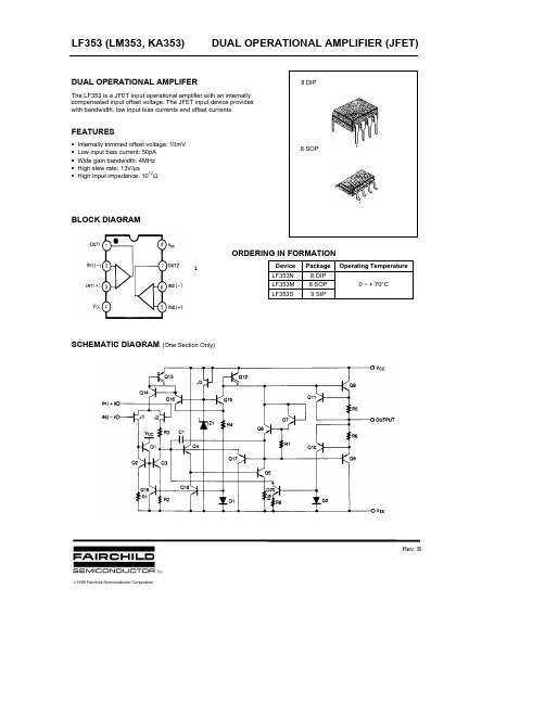
LF353双高阻运算放大器

产品特性● 低功耗● 宽共模(最高为V CC +)、差模电压范围 ● 低输入偏置和失调电流 ● 输出短路保护● 高输入阻抗JFET 输入级 ● 内部频率补偿 ● 无闩锁 ● 高转换速率产品概述该电路为高速JFET 输入双通道运算放大器,单片集成了高匹配、高压JFET 和双极型晶体管。
该器件的特点有高转换速率、低输入偏置和失调电流、低失调电压漂移。
引脚描述(1)金属圆8线 (2)陶瓷双列8线图1 LF353引出端排列(俯视图)电原理图图2 电原理图电参数表表1. LF353电特性,若无其他说明,工作温度为-55℃~+125℃,V CC=±15V。
注1:输入偏置电流是结漏电流,结温每增加10℃,电流值约增加一倍。
绝对最大额定值表2 绝对最大额定值注1:除差模电压外,其他所有电压都是相对于零参考电压(地),即V CC和V CC的中间值。
注2:输入电压的幅度不得超过电源电压和15V二者的较低值。
注3:差分电压是指正相输入端相与反相输入端的电压差。
注4:短路会导致过热和破坏性损耗,各数值为典型值。
注5:输出可能会短路到地或者任一电源,温度或电源电压必须有所限制以保证耗散值不会过大。
应用手册●电压跟随器图3 电压跟随器电路●增益为10的反相放大器图4 增益为10的反相放大器电路封装信息器件采用8引线D型封装和8引线T型封装。
D型封装外形尺寸按GB/T 7092-1993的规定,未注公差的尺寸按GB/T 1804-2000执行,外形尺寸如图5和表3所示。
T型封装外形尺寸按图6和表4的规定。
图5 D型(D08S2)陶瓷双列8线表3 D型(D08S2)封装外形尺寸图6 T型(T08A4)金属圆8线。
LF353中文资料_数据手册_参数
D低输入偏置电流…50 pA型低输入噪声电流0.01 pA/√Hz型低输入噪声电压…18 nV/√Hz型低供电电流…3.6 mA型高输入阻抗…1012年ΩTypD内部削减抵消电压增益带宽……3mhz类型,高转化率…13 V /µs TypdescriptionThis设备是一个低成本、高速、JFET-input运算放大器输入补偿电压很低。
它要求低的供电电流,但LF353保持了一个大的增益带宽产品和快速的转换速度。
此外,调制的高压JFET输入提供非常低的输入偏置和偏置电流。
LF353可用于高速积分器、数模转换器、采样保持电路和许多其他电路。
LF353的特点是在0°C到70°C之间运行。
(每个放大器的输出值+可用选项)包装可用胶带和卷绕。
将后缀R添加到设备类型(即。
LF353DR)。
绝对最大额定参数在操作自由空气的温度范围(除非另外说明)电源电压应用提示(续)由于将输入提高到共模范围内,再次将输入级和放大器置于正常工作模式。
超过单个输入的正共模极限不会改变输出的相位;然而,如果两者都超过了极限,放大器的输出将被迫处于高状态。
放大器的工作将与共模输入电压年龄等于正电源;然而,在这种情况下,增益带宽和旋转速率可能会降低。
当负共模电压荡到负电源的3v以内时,输入偏置伏特可能增加。
每个放大器由齐纳基准分别偏置,允许在±6V功率支持下正常电路运行。
LF353电源电压低于这些可能导致低增益带宽和摆频。
放大器将drivea2kΩ负载电阻±10 v在全温度范围0˚C + 70˚C。
然而,如果放大器被迫驱动更大的负载电流,则可能在负伏特翼上出现输入偏置电压的增加,并最终在正振荡和负振荡上达到有源电流的极限。
LF353应采取措施确保权力supplyfor集成电路不会成为逆转polarityor单位不是无意中安装在asocket向后无限通过resultingforward二极管集成电路中的电流冲击可能导致融合internalconductors和导致破坏单元。
运放的选择

运放的选择:接触过很多电路设计新手,在设计模拟电路时,有的人根本不知道如何选择运放,手头有什么就用什么,也许你曾经这样做了100次,都幸运的成功了,但是第101次会怎么样哪?另外一些人是恰恰相反,抱这五六本原厂资料翻来翻去,结果好不容易寻到了梦中情人,中关村又买不到。
不才向大家推荐一些俗俗的运放,肯定能买到,能适应大多场合。
1. 速度要求不高,或直流放大:LF441(单),LF442(双),LF444(四),TL084(四)(以上运放为JFET输入,阻抗极高,不必考虑输入端的阻抗平衡)OP07(单,高精度,有调零端,速度可是特别慢,用于直流放大不错)2. 速度比较高,音频范围,倍数不超过100:LF356(单),LF353(双),LF347(四),TL074(四)(以上运放为JFET输入,阻抗极高,不必考虑输入端的阻抗平衡)OP27(单,高精度,有调零端,速度比LF356快)NE5534(用于音响放大,音质很好,但输入阻抗低)3. 高速OP37(单位频响50MHz,但一定不能用做跟随器!在闭环增益小于5时会自激)LF441(单),LF442(双),LF444(四),TL084(四)(以上运放为JFET输入,阻抗极高,不必考虑输入端的阻抗平衡)OP07(单,高精度,有调零端,速度可是特别慢,用于直流放大不错)2. 速度比较高,音频范围,倍数不超过100:LF356(单),LF353(双),LF347(四),TL074(四)(以上运放为JFET输入,阻抗极高,不必考虑输入端的阻抗平衡)OP27(单,高精度,有调零端,速度比LF356快)NE5534(用于音响放大,音质很好,但输入阻抗低)3. 高速OP37(单位频响50MHz,但一定不能用做跟随器!在闭环增益小于5时会自激)4. 低压或单电源LM324(四,说实话,我不喜欢它,太慢)CA3130 高输入阻抗运算放大器 Intersil[DATA]CA3140 高输入阻抗运算放大器CD4573 四可编程运算放大器 MC14573ICL7650 斩波稳零放大器LF347(NS[DATA])带宽四运算放大器 KA347LF351 BI-FET单运算放大器 NS[DATA]LF353 BI-FET双运算放大器 NS[DATA]LF356 BI-FET单运算放大器 NS[DATA]LF357 BI-FET单运算放大器 NS[DATA]LF398 采样保持放大器 NS[DATA]LF411 BI-FET单运算放大器 NS[DATA]LF412 BI-FET双运放大器 NS[DATA]LM124 低功耗四运算放大器(军用档) NS[DATA]/TI[DATA] LM1458 双运算放大器 NS[DATA]LM148 四运算放大器 NS[DATA]LM224J 低功耗四运算放大器(工业档) NS[DATA]/TI[DATA] LM2902 四运算放大器 NS[DATA]/TI[DATA]LM2904 双运放大器 NS[DATA]/TI[DATA]LM301 运算放大器 NS[DATA]LM308 运算放大器 NS[DATA]LM308H 运算放大器(金属封装) NS[DATA]LM318 高速运算放大器 NS[DATA]LM324(NS[DATA]) 四运算放大器 HA17324,/LM324N(TI)LM348 四运算放大器 NS[DATA]LM358 NS[DATA] 通用型双运算放大器 HA17358/LM358P(TI) LM380 音频功率放大器 NS[DATA]LM386-1 NS[DATA] 音频放大器 NJM386D,UTC386LM386-3 音频放大器 NS[DATA]LM386-4 音频放大器 NS[DATA]LM3886 音频大功率放大器 NS[DATA]LM3900 四运算放大器LM725 高精度运算放大器 NS[DATA]LM733 带宽运算放大器LM741 NS[DATA] 通用型运算放大器 HA17741 MC34119 小功率音频放大器NE5532 高速低噪声双运算放大器 TI[DATA] NE5534 高速低噪声单运算放大器 TI[DATA] NE592 视频放大器OP07-CP 精密运算放大器 TI[DATA]OP07-DP 精密运算放大器 TI[DATA]TBA820M 小功率音频放大器 ST[DATA]TL061 BI-FET单运算放大器 TI[DATA]TL062 BI-FET双运算放大器 TI[DATA]TL064 BI-FET四运算放大器 TI[DATA]TL072 BI-FET双运算放大器 TI[DATA]TL074 BI-FET四运算放大器 TI[DATA]TL081 BI-FET单运算放大器 TI[DATA]TL082 BI-FET双运算放大器 TI[DATA]TL084 BI-FET四运算放大器 TI[DATA]。
lm353
DUAL OPERATIONAL AMPLIFERThe LF353 is a JFET input operational amplifier with an internally compensated input offset voltage. The JFET input device provides with bandwidth, low input bias currents and offset currents.FEATURES• Internally trimmed offset voltage: 10mV • Low input bias current: 50pA • Wide gain bandwidth: 4MHz • High slew rate: 13V/µs• High Input impedance: 1012ΩBLOCK DIAGRAMORDERING IN FORMATIONiSCHEMATIC DIAGRAM (One Section Only)Device Package Operating TemperatureLF353N 8 DIP LF353M 8 SOP 0 ~ + 70°CLF353S9 SIP©1999 Fairchild Semiconductor CorporationRev. BABSOLUTE MAXIMUM RATINGSELECTRICAL CHARACTERISTICS(V CC =+15V, V EE = -15V, T A =25°C, unless otherwise specified)CharacteristicsSymbol Value Unit Power Supply Voltage Differential Input Voltage Input Voltage Range Output Short Circuit Duration Power DissipationOperating Temperature Range Storage Temperature RangeV CC V I(DIFF)V IP D T OPR T STG ±1830±15Continuous5000 ~ +70-65 ~ +150V V VmW °C °C CharacteristicSymbol Test ConditionsMin Typ Max Unit 5.010°C ≤T A ≤+70°C Input Offset Voltage Drift ∆V IO /∆T R S =10K Ω°C ≤T A ≤+70°C 10 µV/°C 25100pA 0°C ≤T A ≤+70°C4 nA 50200pA 0 °C ≤T A ≤+70°C8nAInput ResistanceR I 1012ΩV O(P-P) = ±0V 25100R L = 2K Ω0°C ≤T A ≤+70°C15 Output Voltage Swing V O(P.P)R L = 10K Ω±12±13.5V Input Voltage RangeV I(R)±11±15/-12V Common Mode Rejection Ratio CMRR R S ≥10K Ω70100dB Power Supply Rejection Ratio PSRR R S ≥10K Ω70100dBPower Supply Current I CC 3.6 6.5mA Slew RateSR G V = 113V/µs Gain-Bandwidth Product GBM 4MHz Channel SeperationCS f = 1Hz ~ 20Khz (Input referenced)120120dB Equivalent Input Noise Voltage V NI R S = 100Ωf = 1KHz 1616nV/√ Equivalent Input Noise CurrentI NIf = 1KHz0.010.01pA/√Hz HzInput Offset Voltage Input Offset Current Input Bias Current Large Signal Voltage Gain G V I BIAS I IO V IO R S =10K ΩV/mV mVTRADEMARKSACEx™CoolFET™CROSSVOLT™E 2CMOS TM FACT™FACT Quiet Series™FAST ®FASTr™GTO™HiSeC™The following are registered and unregistered trademarks Fairchild Semiconductor owns or is authorized to use and is not intended to be an exhaustive list of all such trademarks.LIFE SUPPORT POLICYFAIRCHILD’S PRODUCTS ARE NOT AUTHORIZED FOR USE AS CRITICAL COMPONENTS IN LIFE SUPPORTDEVICES OR SYSTEMS WITHOUT THE EXPRESS WRITTEN APPROV AL OF FAIRCHILD SEMICONDUCTOR CORPORA TION.As used herein:ISOPLANAR™MICROWIRE™POP™PowerTrench™QS™Quiet Series™SuperSOT™-3SuperSOT™-6SuperSOT™-8TinyLogic™1. Life support devices or systems are devices or systems which, (a) are intended for surgical implant intothe body, or (b) support or sustain life, or (c) whosefailure to perform when properly used in accordancewith instructions for use provided in the labeling, can be reasonably expected to result in significant injury to the user.2. A critical component is any component of a lifesupport device or system whose failure to perform can be reasonably expected to cause the failure of the life support device or system, or to affect its safety or effectiveness.PRODUCT STATUS DEFINITIONS Definition of TermsDatasheet Identification Product Status Definition Advance InformationPreliminary No Identification Needed Obsolete This datasheet contains the design specifications for product development. Specifications may change in any manner without notice.This datasheet contains preliminary data, andsupplementary data will be published at a later date.Fairchild Semiconductor reserves the right to make changes at any time without notice in order to improve design.This datasheet contains final specifications. Fairchild Semiconductor reserves the right to make changes at any time without notice in order to improve design.This datasheet contains specifications on a product that has been discontinued by Fairchild semiconductor.The datasheet is printed for reference information only.Formative or In DesignFirst ProductionFull ProductionNot In ProductionDISCLAIMERFAIRCHILD SEMICONDUCTOR RESERVES THE RIGHT TO MAKE CHANGES WITHOUT FURTHER NOTICE TO ANY PRODUCTS HEREIN TO IMPROVE RELIABILITY , FUNCTION OR DESIGN. FAIRCHILD DOES NOT ASSUME ANY LIABILITY ARISING OUT OF THE APPLICATION OR USE OF ANY PRODUCT OR CIRCUIT DESCRIBED HEREIN; NEITHER DOES IT CONVEY ANY LICENSE UNDER ITS PATENT RIGHTS, NOR THE RIGHTS OF OTHERS.。
音频运放使用心得
音频运放使用心得(陈嘉春cjc0412)多年来,玩过众多的运放,我想也到了可以总结的时候了,下面谈谈玩过的一些运放的印象,希望借此抛砖引玉。
首先说双运放,玩过的有:JRC4558、NE5532、CA3240、TL082、TL072、NJM2114、LF353、LM833、MC33078、NE5535、AD8620、AD827、AD828、AD712、OP275、OP285、OP249、OPA2604、OPA2134、OPA2111、OPA2228、OPA2107、LM4562、LME49720、LME49860、EL2224、EL2244、、MUSES01、MUSES02、MUSES8820; 单运放有OPA134、OPA604、OPA627、AD797。
接下来逐一点评:JRC4558:声音尖剌、薄,不愧是臭肉,不浪费文字。
推荐度:★NE5532(全是塑封):电源电压可提高到±18V供电仍然能够正常工作,声音总体偏暖,声场窄、高频有点毛剌,低频肥厚而下潜一般。
几个版本中,当属飞利浦最好,声音平衡度和中频最好听。
ON(安森美)和JRC的版本次之,应该是做了微调,声音比较现代化,高频细节多一些,ON相对更好一些。
再次是大小S的,典型的5532声音,低频特别肥厚,总体不好听。
最差的是TI的5532P,高频剌耳,低频也差。
推荐度:★★☆CA3240:声场窄、高频很一般,但低频非常力度,没有韵味。
推荐度:★★TL082、TL072:声音走清澈路线,声场也较窄,低频下潜一般,但比较耐听。
总体上072要好于082,特点更加突出。
推荐度:★★☆NJM2114:声音比较暖,声场窄,三频平衡度尚可,胜在输出电流大,电源电压可提高到±18V供电仍然能够正常工作,我用在耳放中,8块并联输出推耳机,比5532好许多。
推荐度:★★★LF353:声场窄,声音走清澈路线但解析力一般,用在音频回路没有优势,用在中点伺服上更好。
lf353工作原理
lf353工作原理
LF353是一款专用的宽带高速运算放大器。
该芯片由两个独立的、高性能的运算放大器组成,具有低噪声、高增益带宽和高输入电阻等特点。
它被广泛应用于精密量测和高保真音频放大器等领域。
LF353的工作原理基于差分对输入的放大器电路。
每个运算放大器由一个输入级、一个差动放大级和一个输出级组成。
输入级对输入信号进行阻抗扩展,并将信号传递给差动放大级。
差动放大器使用两个晶体管配对,将差分输入信号放大,并通过输出级将放大的信号输出。
在工作时,差分输入信号被分别连接到运放的非反相和反相输入端。
当输入信号的差异引起非线性失真时,差动放大器会通过增益控制来抵消这种失真。
差动放大器的增益与输出信号的相位差紧密相关,从而实现了对输入信号的线性放大。
LF353还具有高输入阻抗,这意味着它对输入信号的负载影响很小,从而使得输入信号的失真减小。
同时,该芯片的低噪声特性使其能够接收较小幅度的输入信号,并输出高保真度的放大信号。
总之,LF353的工作原理基于差分输入的放大器电路结构,通过差动放大器将输入信号放大,并通过输出级输出放大信号。
它的高增益带宽、低噪声和高输入阻抗等特性使其成为广泛应用于各种精密测量和音频放大器应用的理想选择。
- 1、下载文档前请自行甄别文档内容的完整性,平台不提供额外的编辑、内容补充、找答案等附加服务。
- 2、"仅部分预览"的文档,不可在线预览部分如存在完整性等问题,可反馈申请退款(可完整预览的文档不适用该条件!)。
- 3、如文档侵犯您的权益,请联系客服反馈,我们会尽快为您处理(人工客服工作时间:9:00-18:30)。
LF353Wide Bandwidth Dual JFET Input Operational AmplifierGeneral DescriptionThese devices are low cost,high speed,dual JFET input operational amplifiers with an internally trimmed input offset voltage (BI-FET II ™technology).They require low supply current yet maintain a large gain bandwidth product and fast slew rate.In addition,well matched high voltage JFET input devices provide very low input bias and offset currents.The LF353is pin compatible with the standard LM1558allowing designers to immediately upgrade the overall performance of existing LM1558and LM358designs.These amplifiers may be used in applications such as high speed integrators,fast D/A converters,sample and hold circuits and many other circuits requiring low input offset voltage,low input bias current,high input impedance,high slew rate and wide bandwidth.The devices also exhibit low noise and offset voltage drift.Featuresn Internally trimmed offset voltage:10mV n Low input bias current:50pA n Low input noise voltage:25nV/√Hz n Low input noise current:0.01pA/√Hzn Wide gain bandwidth:4MHz n High slew rate:13V/µs n Low supply current: 3.6mA n High input impedance:1012Ωn Low total harmonic distortion :≤0.02%n Low 1/f noise corner:50Hz nFast settling time to 0.01%:2µsTypical Connection 00564914Simplified Schematic1/2Dual00564916Connection DiagramDual-In-Line Package00564917Top ViewOrder Number LF353M,LF353MX or LF353N See NS Package Number M08A or N08EBI-FET II ™is a trademark of National Semiconductor Corporation.December 2003LF353Wide Bandwidth Dual JFET Input Operational Amplifier©2003National Semiconductor Corporation Absolute Maximum Ratings (Note1)If Military/Aerospace specified devices are required,please contact the National Semiconductor Sales Office/Distributors for availability and specifications.Supply Voltage ±18VPower Dissipation(Note 2)Operating Temperature Range 0˚C to +70˚CT j (MAX)150˚CDifferential Input Voltage ±30V Input Voltage Range (Note 3)±15VOutput Short Circuit Duration Continuous Storage Temperature Range −65˚C to +150˚CLead Temp.(Soldering,10sec.)260˚CSoldering Information Dual-In-Line Package Soldering (10sec.)260˚CSmall Outline Package Vapor Phase (60sec.)215˚C Infrared (15sec.)220˚CSee AN-450“Surface Mounting Methods and Their Effect on Product Reliability”for other methods of soldering surface mount devices.ESD Tolerance (Note 8)1000V θJA M PackageTBDNote 1:Absolute Maximum Ratings indicate limits beyond which damage to the device may occur.Operating ratings indicate conditions for which the device is functional,but do not guarantee specific performance limits.Elec-trical Characteristics state DC and AC electrical specifications under particu-lar test conditions which guarantee specific performance limits.This assumes that the device is within the Operating Ratings.Specifications are not guar-anteed for parameters where no limit is given,however,the typical value is a good indication of device performance.DC Electrical Characteristics(Note 5)Symbol ParameterConditionsLF353Units MInTyp Max V OS Input Offset VoltageR S =10k Ω,T A =25˚C 510mV Over Temperature 13mV ∆V OS /∆T Average TC of Input Offset Voltage R S =10k Ω10µV/˚C I OS Input Offset Current T j =25˚C,(Notes 5,6)25100pA T j ≤70˚C4nA I B Input Bias Current T j =25˚C,(Notes 5,6)50200pA T j ≤70˚C 8nA R IN Input ResistanceT j =25˚C1012ΩA VOLLarge Signal Voltage GainV S =±15V,T A =25˚C 25100V/mVV O =±10V,R L =2k ΩOver Temperature15V/mVV O Output Voltage Swing V S =±15V,R L =10k Ω±12±13.5V V CM Input Common-Mode Voltage V S =±15V±11+15V Range−12V CMRR Common-Mode Rejection Ratio R S ≤10k Ω70100dB PSRR Supply Voltage Rejection Ratio (Note 7)70100dB I SSupply Current3.66.5mAAC Electrical Characteristics(Note 5)SymbolParameterConditionsLF353UnitsMinTyp MaxAmplifier to Amplifier CouplingT A =25˚C,f=1Hz−20kHz −120dB (Input Referred)SR Slew RateV S =±15V,T A =25˚C 8.013V/µs GBW Gain Bandwidth Product V S =±15V,T A =25˚C 2.74MHze n Equivalent Input Noise Voltage T A =25˚C,R S =100Ω,16f=1000Hzi nEquivalent Input Noise CurrentT j =25˚C,f=1000Hz0.01L F 353 2AC Electrical Characteristics (Continued)(Note5)Symbol Parameter Conditions LF353UnitsMin Typ MaxTHD Total Harmonic Distortion A V=+10,RL=10k,V O=20Vp−p,BW=20Hz-20kHz<0.02%Note2:For operating at elevated temperatures,the device must be derated based on a thermal resistance of115˚C/W typ junction to ambient for the N package, and158˚C/W typ junction to ambient for the H package.Note3:Unless otherwise specified the absolute maximum negative input voltage is equal to the negative power supply voltage.Note4:The power dissipation limit,however,cannot be exceeded.Note5:These specifications apply for V S=±15V and0˚C≤T A≤+70˚C.V OS,I B and I OS are measured at V CM=0.Note6:The input bias currents are junction leakage currents which approximately double for every10˚C increase in the junction temperature,T j.Due to the limited production test time,the input bias currents measured are correlated to junction temperature.In normal operation the junction temperature rises above the ambient temperature as a result of internal power dissipation,P D.T j=T A+θjA P D whereθjA is the thermal resistance from junction to e of a heat sink is recommended if input bias current is to be kept to a minimum.Note7:Supply voltage rejection ratio is measured for both supply magnitudes increasing or decreasing simultaneously in accordance with common practice.V S =±6V to±15V.Note8:Human body model,1.5kΩin series with100pF.Typical Performance CharacteristicsInput Bias Current Input Bias Current0056491800564919Supply Current Positive Common-Mode Input Voltage Limit0056492000564921LF3533Typical Performance Characteristics(Continued)Negative Common-Mode Input Voltage LimitPositive Current Limit0056492200564923Negative Current Limit Voltage Swing0056492400564925Output Voltage Swing Gain Bandwidth0056492600564927L F 353 4Typical Performance Characteristics(Continued)Bode PlotSlew Rate0056492800564929Distortion vs.Frequency Undistorted Output Voltage Swing0056493000564931Open Loop Frequency Response Common-Mode Rejection Ratio0056493200564933LF3535Typical Performance Characteristics(Continued)Power Supply Rejection RatioEquivalent Input Noise Voltage0056493400564935Open Loop Voltage Gain (V/V)Output Impedance0056493600564937Inverter Settling Time00564938L F 353 6Pulse ResponseSmall Signaling Inverting00564904Large Signal Inverting00564906Small Signal Non-Inverting00564905Large Signal Non-Inverting00564907Current Limit(R L=100Ω)00564908Application HintsThese devices are op amps with an internally trimmed inputoffset voltage and JFET input devices(BI-FET II).TheseJFETs have large reverse breakdown voltages from gate tosource and drain eliminating the need for clamps across theinputs.Therefore,large differential input voltages can easilybe accommodated without a large increase in input current.The maximum differential input voltage is independent of thesupply voltages.However,neither of the input voltagesshould be allowed to exceed the negative supply as this willcause large currents to flow which can result in a destroyedunit.Exceeding the negative common-mode limit on either inputwill force the output to a high state,potentially causing areversal of phase to the output.Exceeding the negativecommon-mode limit on both inputs will force the amplifieroutput to a high state.In neither case does a latch occurLF3537Application Hints(Continued)sinceraising the input back within the common-mode range again puts the input stage and thus the amplifier in a normal operating mode.Exceeding the positive common-mode limit on a single input will not change the phase of the output;however,if both inputs exceed the limit,the output of the amplifier will be forced to a high state.The amplifiers will operate with a common-mode input volt-age equal to the positive supply;however,the gain band-width and slew rate may be decreased in this condition.When the negative common-mode voltage swings to within 3V of the negative supply,an increase in input offset voltage may occur.Each amplifier is individually biased by a zener reference which allows normal circuit operation on ±6V power sup-plies.Supply voltages less than these may result in lower gain bandwidth and slew rate.The amplifiers will drive a 2k Ωload resistance to ±10V over the full temperature range of 0˚C to +70˚C.If the amplifier is forced to drive heavier load currents,however,an increase in input offset voltage may occur on the negative voltage swing and finally reach an active current limit on both posi-tive and negative swings.Precautions should be taken to ensure that the power supply for the integrated circuit never becomes reversed in polarityor that the unit is not inadvertently installed backwards in a socket as an unlimited current surge through the resulting forward diode within the IC could cause fusing of the internal conductors and result in a destroyed unit.As with most amplifiers,care should be taken with lead dress,component placement and supply decoupling in order to ensure stability.For example,resistors from the output to an input should be placed with the body close to the input to minimize “pick-up”and maximize the frequency of the feed-back pole by minimizing the capacitance from the input to ground.A feedback pole is created when the feedback around any amplifier is resistive.The parallel resistance and capacitance from the input of the device (usually the inverting input)to AC ground set the frequency of the pole.In many instances the frequency of this pole is much greater than the expected 3dB frequency of the closed loop gain and consequently there is negligible effect on stability margin.However,if the feed-back pole is less than approximately 6times the expected 3dB frequency a lead capacitor should be placed from the output to the input of the op amp.The value of the added capacitor should be such that the RC time constant of this capacitor and the resistance it parallels is greater than or equal to the original feedback pole time constant.Detailed Schematic00564909L F 353 8Typical ApplicationsThree-Band Active Tone Control0056493900564940Note 1:All controls flat.Note 2:Bass and treble boost,mid flat.Note 3:Bass and treble cut,mid flat.Note 4:Mid boost,bass and treble flat.Note 5:Mid cut,bass and treble flat.•All potentiometers are linear taper•Use the LF347Quad for stereo applicationsLF3539Typical Applications(Continued)Improved CMRR Instrumentation Amplifier00564941Fourth Order Low Pass Butterworth Filter00564942L F 353 10Typical Applications (Continued)Fourth Order High Pass Butterworth Filter0056494311Typical Applications (Continued)Ohms to Volts Converter00564944L F 12Physical Dimensions inches (millimeters)unless otherwise notedOrder Number LF353M or LF353MXNS Package Number M08AMolded Dual-In-Line PackageOrder Number LF353NNS Package N08E13Notes LIFE SUPPORT POLICYNATIONAL’S PRODUCTS ARE NOT AUTHORIZED FOR USE AS CRITICAL COMPONENTS IN LIFE SUPPORT DEVICES OR SYSTEMS WITHOUT THE EXPRESS WRITTEN APPROVAL OF THE PRESIDENT AND GENERAL COUNSEL OF NATIONAL SEMICONDUCTOR CORPORATION.As used herein:1.Life support devices or systems are devices orsystems which,(a)are intended for surgical implantinto the body,or (b)support or sustain life,andwhose failure to perform when properly used inaccordance with instructions for use provided in thelabeling,can be reasonably expected to result in asignificant injury to the user.2.A critical component is any component of a life support device or system whose failure to perform can be reasonably expected to cause the failure of the life support device or system,or to affect its safety or effectiveness.BANNED SUBSTANCE COMPLIANCENational Semiconductor certifies that the products and packing materials meet the provisions of the Customer Products Stewardship Specification (CSP-9-111C2)and the Banned Substances and Materials of Interest Specification (CSP-9-111S2)and contain no ‘‘Banned Substances’’as defined in CSP-9-111S2.National SemiconductorAmericas CustomerSupport CenterEmail:new.feedback@Tel:1-800-272-9959National Semiconductor Europe Customer Support Center Fax:+49(0)180-5308586Email:europe.support@ Deutsch Tel:+49(0)6995086208English Tel:+44(0)8702402171Français Tel:+33(0)141918790National Semiconductor Asia Pacific Customer Support Center Email:ap.support@ National Semiconductor Japan Customer Support Center Fax:81-3-5639-7507Email:jpn.feedback@ Tel: L F 353W i d e B a n d w i d t h D u a l J F E T I n p u t O p e r a t i o n a l A m p l i f i e r National does not assume any responsibility for use of any circuitry described,no circuit patent licenses are implied and National reserves the right at any time without notice to change said circuitry and specifications.。