'MCP41010中文资料
MCP79410中文版本
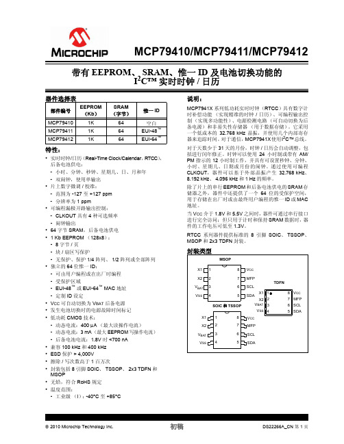
表 1-1:
直流特性 参数 编号 — D1 D2 D3 D4 D5 D6 D7 D8 VIH VIL VHYS VOL ILI ILO CIN, COUT 符号
直流特性
电气特性: 工业级 (I) : 特性 SCL 和 SDA 引脚 高电平输入电压 低电平输入电压 施密特触发器输入的迟滞 电压 (SDA 和 SCL 引脚) 低电平输出电压 (MFP 和 SDA) 输入泄漏电流 输出泄漏电流 引脚电容 (SDA、 SCL 和 MFP) 最小值 — 0.7 VCC — 0.05 VCC — — — — — — — — — — 1.3 300 0 1.3 5.5 700 VCC = +1.8V 至 5.5V 单位 — V V V V μA μA pF μA mA μA μA μA nA V μs μs V — — VCC = 2.5V 至 5.5V (注 1) VCC = 4.5V 时, IOL = 3.0 mA VCC = 2.5V 时, IOL = 2.1 mA VIN = VSS 或 VCC VOUT = VSS 或 VCC VCC = 5.0V (注 1) TA = 25°C, f = 400 kHz VCC = 5.5V, SCL = 400 kHz VCC = 5.5V VCC = 5.5V, SCL = 400 kHz VCC = 5.5V, SCL = 400 kHz VCC = 5.5V, SCL = SDA = VCC 25°C 时 VBAT = 1.8V TAMB = 25°C 时典型值为 1.5V 从 VTRIP (最大值)到 VTRIP (最小值) 从 VTRIP (最小值)到 VTRIP (最大值) — TA = -40°C 至 +85°C 条件
THD:STA 启动条件保持时间 TSU:STA 启动条件建立时间
HDSP-N401-00000中文资料

Features• Low Power Consumption • Industry Standard Size• Industry Standard Pinout • Choice of Character Size7.6 mm (0.30 in), 10 mm (0.40 in), 10.9 mm (0.43 in), 14.2 mm (0.56 in), 20 mm (0.80 in)• Choice of ColorsAlGaAs Red, High Efficiency Red (HER), Yellow, Green• Excellent Appearance Evenly Lighted Segments±50° Viewing Angle• Design FlexibilityCommon Anode or Common CathodeSingle and Dual DigitLeft and Right Hand Decimal Points±1. Overflow Character• Categorized for Luminous IntensityYellow and Green Categorized for ColorUse of Like Categories Yields a Uniform Display• Excellent for Long Digit String Multiplexing DescriptionThese low current seven segment displays are designed for applica-tions requiring low power consumption. They are tested and selected for their excellent low current characteristics to ensure that the segments are matched at low currents. Drive currents as low as 1 mA per segment are available.Pin for pin equivalent displays are also available in a standard current or high light ambient design. The standard current displays are available in all colors and are ideal for most applica-tions. The high light ambient displays are ideal for sunlight ambients or long string lengths. For additional information see the 7.6 mm Micro Bright Seven Segment Displays, 10 mm Seven Segment Displays, 7.6 mm/10.9 mm Seven Segment Displays, 14.2 mm Seven Segment Displays, 20 mm Seven Segment Displays, or High Light Ambient Seven Segment Displays data sheets.Low Current Seven SegmentDisplays Technical Data HDSP-335x SeriesHDSP-555x SeriesHDSP-751x SeriesHDSP-A10x Series HDSP-A80x Series HDSP-A90x Series HDSP-E10x Series HDSP-F10x Series HDSP-G10x Series HDSP-H10x Series HDSP-K12x, K70x Series HDSP-N10x SeriesHDSP-N40x SeriesDevicesAlGaAs HER Yellow Green Package HDSP-HDSP-HDSP-HDSP-Description Drawing A1017511A801A9017.6 mm Common Anode Right Hand Decimal A A1037513A803A9037.6 mm Common Cathode Right Hand Decimal B A1077517A807A9077.6 mm Common Anode ±1. Overflow C A1087518A808A9087.6 mm Common Cathode ±1. Overflow D F10110 mm Common Anode Right Hand Decimal E F10310 mm Common Cathode Right Hand Decimal F F10710 mm Common Anode ±1. Overflow G F10810 mm Common Cathode ±1. Overflow H G10110 mm Two Digit Common Anode Right Hand Decimal X G10310 mm Two Digit Common Cathode Right Hand Decimal Y E100335010.9 mm Common Anode Left Hand Decimal I E101335110.9 mm Common Anode Right Hand Decimal J E103335310.9 mm Common Cathode Right Hand Decimal K E106335610.9 mm Universal ±1. Overflow[1]L H101555114.2 mm Common Anode Right Hand Decimal M H103555314.2 mm Common Cathode Right Hand Decimal N H107555714.2 mm Common Anode ±1. Overflow O H108555814.2 mm Common Cathode ±1. Overflow P K121K70114.2 mm Two Digit Common Anode Right Hand Decimal R K123K70314.2 mm Two Digit Common Cathode Right Hand Decimal S N10020 mm Common Anode Left Hand Decimal Q N101N40120 mm Common Anode Right Hand Decimal T N103N40320 mm Common Cathode Right Hand Decimal U N10520 mm Common Cathode Left Hand Decimal V N106N40620 mm Universal ±1. Overflow[1]W Note:1. Universal pinout brings the anode and cathode of each segment’s LED out to separate pins. See internal diagrams L or W.Part Numbering System5082-x xx x-x x x xxHDSP-x xx x-x x x xxMechanical Options[1]00: No mechanical optionColor Bin Options[1,2]0: No color bin limitationMaximum Intensity Bin[1,2]0: No maximum intensity bin limitationMinimum Intensity Bin[1,2]0: No minimum intensity bin limitationDevice Configuration/Color[1]G: GreenDevice Specific Configuration[1]Refer to respective datasheetPackage[1]Refer to Respective datasheetNotes:1. For codes not listed in the figure above, please refer to the respective datasheet or contact your nearest Agilent representative fordetails.2. Bin options refer to shippable bins for a part-number. Color and Intensity Bins are typically restricted to 1 bin per tube (excep-tions may apply). Please refer to respective datasheet for specific bin limit information.Package DimensionsPackage Dimensions (cont.)Package Dimensions (cont.)*The Side View of package indicates Country of Origin.Package Dimensions (cont.)Package Dimensions (cont.)Package Dimensions (cont.)Internal Circuit DiagramInternal Circuit Diagram (cont.)Absolute Maximum RatingsAlGaAs Red - HDSP-HERA10X/E10X/H10X HDSP-751X/Yellow GreenK12X/N10X/N40X335X/555X/HDSP-A80X HDSP-A90X Description F10X, G10X Series K70X Series Series Series Units Average Power per Segment or DP375264mW Peak Forward Current per 45mA Segment or DPDC Forward Current per15[1]15[2]mA Segment or DPOperating Temperature Range-20 to +100-40 to +100°C Storage Temperature Range -55 to +100°C Reverse Voltage per Segment 3.0V or DPWave Soldering Temperature for 3Seconds (1.60 mm [0.063 in.] below 250°C seating body)Notes:1. Derate above 91°C at 0.53 mA/°C.2. Derate HER/Yellow above 80°C at 0.38 mA/°C and Green above 71°C at 0.31 mA/°C.Electrical/Optical Characteristics at T A = 25°CAlGaAs RedDeviceSeriesHDSP-Parameter Symbol Min.Typ.Max.Units Test Conditions315600I F = 1 mA A10x3600I F = 5 mA330650I F = 1 mAF10x, G10x3900I F = 5 mA390650I F = 1 mA E10x Luminous Intensity/Segment[1,2]I Vµcd(Digit Average)3900I F = 5 mA400700I F = 1 mAH10x, K12x4200I F = 5 mA270590I F = 1 mAN10x, N40x3500I F = 5 mA1.6I F = 1 mAForward Voltage/Segment or DP V F 1.7V I F = 5 mA1.82.2I F = 20 mA PkAll Devices Peak WavelengthλPEAK645nmDominant Wavelength[3]λd637nmReverse Voltage/Segment or DP[4]V R 3.015V I R = 100 µATemperature Coefficient of∆V F/°C-2 mV mV/°CV F/Segment or DPA10x255F10x, G10x320E10x340Thermal Resistance LED RθJ-PIN°C/W/SegH10x, K12x Junction-to-Pin400N10x, N40x430High Efficiency RedDeviceSeriesHDSP-Parameter Symbol Min.Typ.Max.Units Test Conditions160270I F = 2 mA 751x1050I F = 5 mA200300I F = 2 mA Luminous Intensity/Segment[1,2]I V mcd(Digit Average)1200I F = 5 mA335x, 555x,K70x270370I F = 2 mA1480I F = 5 mA1.6I F = 2 mAForward Voltage/Segment or DP V F 1.7V I F = 5 mA2.1 2.5I F = 20 mA Pk All Devices Peak WavelengthλPEAK635nmDominant Wavelength[3]λd626nmReverse Voltage/Segment or DP[4]V R 3.030V I R = 100 µATemperature Coefficient of∆V F/°C-2mV/°CV F/Segment or DP751x200335x Thermal Resistance LED RθJ-PIN280°C/WJunction-to-Pin555x, K70x345YellowDeviceSeriesHDSP-Parameter Symbol Min.Typ.Max.Units Test Conditions Luminous Intensity/Segment[1,2]250420I F = 4 mA(Digit Average)I V mcd1300I F = 10 mA1.7I F = 4 mAForward Voltage/Segment or DP V F 1.8V I F = 5 mA A80x2.1 2.5I F = 20 mA PkPeak WavelengthλPEAK583nmDominant Wavelength[3,5]λd581.5585592.5nmReverse Voltage/Segment or DP[4]V R 3.030V I R = 100 µATemperature Coefficient of∆V F/°C-2mV/°CV F/Segment or DPThermal Resistance LED RθJ-PIN200°C/WJunction-to-PinGreenDeviceSeriesHDSP-Parameter Symbol Min.Typ.Max.Units Test Conditions Luminous Intensity/Segment[1,2]250475I F = 4 mA(Digit Average)I V mcd1500I F = 10 mA1.9I F = 4 mAForward Voltage/Segment or DP V F 2.0V I F = 10 mA A90x2.1 2.5I F = 20 mA PkPeak WavelengthλPEAK566nmDominant Wavelength[3,5]λd571577nmReverse Voltage/Segment or DP[4]V R 3.030V I R = 100 µATemperature Coefficient of∆V F/°C-2mV/°CV F/Segment or DPThermal Resistance LED RθJ-PIN200°C/WJunction-to-PinNotes:1. Device case temperature is 25°C prior to the intensity measurement.2. The digits are categorized for luminous intensity. The intensity category is designated by a letter on the side of the package.3. The dominant wavelength, λd, is derived from the CIE chromaticity diagram and is the single wavelength which defines the color of thedevice.4. Typical specification for reference only. Do not exceed absolute maximum ratings.5. The yellow (HDSP-A800) and Green (HDSP-A900) displays are categorized for dominant wavelength. The category is designated by anumber adjacent to the luminous intensity category letter.AlGaAs RedIntensity Bin Limits (mcd)AlGaAs RedHDSP-A10xIV Bin Category Min.Max.E0.3150.520F0.4280.759G0.621 1.16H0.945 1.71I 1.40 2.56J 2.10 3.84K 3.14 5.75L 4.708.55HDSP-E10x/F10x/G10xIV Bin Category Min.Max.D0.3910.650E0.5320.923F0.755 1.39G 1.13 2.08H 1.70 3.14HDSP-H10x/K12xIV Bin Category Min.Max.C0.4150.690D0.5650.990E0.810 1.50F 1.20 2.20G 1.80 3.30H 2.73 5.00I 4.097.50HDSP-N10xIV Bin Category Min.Max.A0.2700.400B0.3250.500C0.4150.690D0.5650.990E0.810 1.50F 1.20 2.20G 1.80 3.30H 2.73 5.00I 4.097.50Intensity Bin Limits (mcd), continued HERHDSP-751xIV Bin Category Min.Max.B0.1600.240C0.2000.300D0.2500.385E0.3150.520F0.4280.759G0.621 1.16HDSP-751xIV Bin Category Min.Max.B0.2400.366C0.3000.477D0.3910.650E0.5320.923F0.755 1.39G 1.13 2.08H 1.70 3.14HDSP-555x/K70xIV Bin Category Min.Max.A0.2700.400B0.3250.500C0.4150.690D0.5650.990E0.810 1.50F 1.20 2.20G 1.80 3.30H 2.73 5.00I 4.097.50Intensity Bin Limits (mcd), continued YellowHDSP-A80xIV Bin Category Min.Max.D0.2500.385E0.3150.520F0.4250.760G0.625 1.14H0.940 1.70I 1.40 2.56J 2.10 3.84K 3.14 5.76L 4.718.64M7.0713.00N10.6019.40O15.9029.20P23.9043.80Q35.8065.60GreenHDSP-A90xIV Bin Category Min.Max.E0.3150.520F0.4250.760G0.625 1.14H0.940 1.70I 1.40 2.56J 2.10 3.84K 3.14 5.76L 4.718.64M7.0713.00N10.6019.40O15.9029.20P23.9043.80Q35.8065.60Electrical/OpticalFor more information on electrical/optical characteristics, please see Application Note 1005.Contrast Enhancement For information on contrast enhancement, please see Application Note 1015.Soldering/Cleaning Cleaning agents from the ketone family (acetone, methyl ethyl ketone, etc.) and from the chorinated hydrocarbon family (methylene chloride, trichloro-ethylene, carbon tetrachloride, etc.) are not recommended for cleaning LED parts. All of these various solvents attack or dissolve the encapsulating epoxies used to form the package of plastic LED parts.For information on soldering LEDs, please refer to Application Note 1027.Note:All categories are established for classification of products. Productsmay not be available in all categories. Please contact your localAgilent representatives for further clarification/information.Color Categories/semiconductorsFor product information and a complete list ofdistributors, please go to our web site.For technical assistance call:Americas/Canada: +1 (800) 235-0312 or(916) 788 6763Europe: +49 (0) 6441 92460China: 10800 650 0017Hong Kong: (+65) 6271 2451India, Australia, New Zealand: (+65) 6271 2394Japan: (+81 3) 3335-8152(Domestic/International), or0120-61-1280(Domestic Only)Korea: (+65) 6271 2194Malaysia, Singapore: (+65) 6271 2054Taiwan: (+65) 6271 2654Data subject to change.Copyright © 2005 Agilent Technologies, Inc.Obsoletes 5988-8412ENJanuary 19, 20055989-0080EN。
MCP41010数据手册中文版

抽头控制 电阻 寄存器 阵列 1*
PDIP/SOIC/TSSOP
CS SCK SI VSS PB1 PW1 PA1 1 2 14 13 VDD SO SHDN RS PB0 PW0 PA0
MCP42XXX
3 4 5 6 7
12 11 10 9 8
* 只有在双 MCP42XXX 器件上才有电位器 P1。
DS11195C_CN 第 2 页
2006 Microchip Technology Inc.
MCP41XXX/42XXX
直流特性:50 kΩ 器件
电气特性:除非另外声明,否则 VDD = +2.7V 至 5.5V 且 TA = -40°C 至 +85°C (规定 TSSOP 器件只能在 +25°C 和 +85°C 条件下工作) 。 典型规范值:VDD = 5V、 VSS = 0V、 VB = 0V 且 TA = +25°C。 参数 变阻器模式 标称电阻 变阻器差分非线性度 变阻器积分非线性度 变阻器温度系数 抽头电阻 抽头电流 标称电阻匹配 电位器分压器 分辨率 单调性 差分非线性度 积分非线性度 分压器温度系数 满量程误差 零刻度误差 电阻端子 电压范围 电容 (CA 或 CB) 电容 动态特性 (测试所有动态特性时 VDD = 5V) 带宽 -3dB 稳定时间 电阻噪声电压 串扰 施密特触发器高电平输入电压 施密特触发器低电平输入电压 施密特触发器输入迟滞 低输出电压 高输出电压 输入泄漏电流 引脚电容 (所有输入 / 输出) 电源要求 工作电压范围 输入电流,有源 输入电流,静态 电源灵敏度 注 1: 2: 3: 4: 5: 6: VDD IDDA IDDS PSS PSS 2.7 - - - - - 340 0.01 0.0015 0.0015 5.5 500 1 0.0035 0.0035 V µA µA %/% %/% VDD = 5.5V, CS = VSS, fSCK = 10 MHz, SO = 开路,编码 FFh (注 6) CS, SHDN, RS = VDD = 5.5V, SO = 开路 (注 6) VDD = 4.5V - 5.5V, VA = 4.5V,编码 80h VDD = 2.7V - 3.3V, VA = 2.7V,编码 80h BW tS eNWB CT VIH VIL VHYS VOL VOH ILI CIN, COUT - - - - 0.7VDD - - - VDD - 0.5 -1 - 280 8 20 -95 - - .05VDD - - - 10 - - - - - .3VDD - 0.40 - +1 - V V µA pF IOL = 2.1 mA, VDD = 5V IOH = -400 µA, VDD = 5V CS = VDD, VIN = VSS 或 VDD,包括 VA SHDN=0 VDD = 5.0V, TA = +25°C, fc = 1 MHz MHz µS nV/√Hz dB V V VB = 0V,在编码为 80h,输出负载 = 30 µF 时测 得 VA = VDD, VB = 0V,误差范围为 ±1%,从编码 00h 过渡到 80h,输出负载 = 30 pF VA = 开路,编码 80h, f = 1 kHz VA = VDD, VB = 0V (注 5) CW VA,B,W 0 - - - 11 5.6 VDD - - pF pF 注4 f = 1 MHz,编码 = 80h,请参见图 2-30 f =1 MHz,编码 = 80h,请参见图 2-30 N N DNL INL ∆VW/∆T VWFSE VWFSE VWZSE VWZSE 8 8 -1 -1 - -1 -1 0 0 - - ±1/4 ±1/4 1 -0.25 -0.35 +0.25 +0.35 - - +1 +1 - 0 0 +1 +1 位 位 LSB LSB LSB LSB LSB LSB 注3 注3 编码 FFh, VDD = 5V,请参见图 2-25 编码 FFh, VDD = 3V,请参见图 2-25 编码 00h, VDD = 5V,请参见图 2-25 编码 00h, VDD = 3V,请参见图 2-25 R R-DNL R-INL ∆RAB/∆T RW RW IW ∆R/R 35 -1 -1 - - - -1 - 50 ±1/4 ±1/4 800 125 175 - 0.2 65 +1 +1 - 175 250 +1 1 kΩ LSB LSB ppm/°C Ω Ω mA % 仅 MCP42050, P0 到 P1 ; TA = +25°C VDD = 5.5V, IW = 1 mA,编码 00h VDD = 2.7V, IW = 1 mA,编码 00h TA = +25°C (注 1) 注2 注2 符号 最小值 典型值 最大值 单位 条件
MCP41010中文 数字电位器

电源灵敏度
注
1:
2:
3:
4: 5: 6:
PSS
-
0.0015 0.0035 %/% VDD = 4.5V - 5.5V, VA = 4.5V,编码 80h
PSS
-
0.0015 0.0035 %/% VDD = 2.7V - 3.3V, VA = 2.7V,编码 80h
0
LSB 编码 FFh, VDD = 3V,请参见图 2-25
VWZSE
0
+0.25
+1
LSB 编码 00h, VDD = 5V,请参见图 2-25
VWZSE
0
+0.35
+1
LSB 编码 00h, VDD = 3V,请参见图 2-25
电压范围
VA,B,W
0
-
VDD
注4
电容 (CA 或 CB)
-
11
-
VOL
-
-
VOH
VDD - 0.5
-
ILI
-1
-
CIN, COUT
-
10
0.40 - +1 -
V
IOL = 2.1 mA, VDD = 5V
V
IOH = -400 µA, VDD = 5V
µA CS = VDD, VIN = VSS 或 VDD,包括 VA SHDN=0
pF VDD = 5.0V, TA = +25°C, fc = 1 MHz
-
RW
-
RW
-
IW
-1
∆R/R
-
800
-
ppm/°C
52
100
Ω VDD = 5.5V、 IW = 1 mA、编码 00h
MCP1401_02中文数据资料

图 2-10: 静态电流-温度关系曲线
Input Threshold (V)
2.2
2.1
VHI
2
1.9
1.8
1.7
VLO
1.6
1.5
4
6
8 10 12 14 16 18
Supply Voltage (V)
图 2-11: 输入阈值-电源电压关系曲线
Quiescent Current (mA)
1.2
1.0
30 VDD = 12V
26
22
tRISE tFALL
Time (ns)
18
14
10 -40 -25 -10 5 20 35 50 65 80 95 110 125
Temperature (oC)
图 2-3: 上升和下降时间-温度关系曲线
Propagation Delay (ns)
44 43 42 41 40 39 38 37 36
MCP1401/02 器件可由 4.5V 至 18V 的单电源供电,且 可轻松地在不到 19 ns(典型值)的时间内对 470 pF 的 栅极电容进行充放电。 在导通和关断状态下,均可提供 足够低的阻抗,以确保即使有很大的瞬态信号也不会影 响 MOSFET 的预期状态。
只要在其功率和电压范围内,任何情况下这些器件都很 难闭锁。 当接地端出现幅度小于等于 5V (任何极性) 的噪声尖峰时,这些器件也不会损坏。它们能承受大小 在 500 mA 内的反向电流灌入其输出端,而不会损坏或 出现逻辑颠倒。 此外,所有引脚都被充分地保护,能承 受最高为 3 kV (HBM)和 400V (MM)的静电放电 (Electro-static Discharge, ESD)。
精确电压基准MCP1525、MCP1541中文资料

2.5Vਜ਼4.096V࢟ኹᓰ—M C P1525/1541特性z精确电压基准z输出电压2.5V和4.096Vz初始精度:最大1%z温度漂移: 最大50ppm/z输出电流驱动: 2mAz最大操作电流:最大100A@25z TO-92,SOT23-3封装z工业级温度范围:-4085应用z电池供电系统z手持设备z仪器和过程控制z测试设备z数据采集系统z通讯设备z医疗设备z精密功率供给电源z8位,10位,12位A/D转换器z D/A转换器描述Microchip公司的MCP1525和MCP1541设备是2.5V和4.096V精确电压基准,它们采用了先进的CMOS电路和EPROM微调技术的组合所以该器件可以达到1%最大的初始精度和最大50ppm/¢的温漂同时在25时静态电流可以低至100A最大,这些设备在超过时间和温度时还提供一个优于传统齐纳技术的新特性.MCP1525的输出电压为2.5V,MCP1541为4.096V.这些器件采用TO-92和SOT23-3封装,工业级温度范围:-4085.器件选择表封装MCP1541温度漂移1.0 电特性1.1 最大范围V IN 7.0V输入电流(V IN) 20mA输出电流(V OUT) 20mA连续电压损耗(T A=15) 140mW所有输入和输出w.r.t -0.6V~(V IN+1.0V)存储温度 -65150输入电压时环境温度 -55125对所有引脚的ESD保护4kV电特性说明 1.输出电压滞后指25时测量的输出电压在温度从85变化到-40前后的电压变化.2.输出温度系数用一个”BOX”的方法来测量,其方法是在25时将输出电压尽量修整为典型值,然后85时输出电压再次被修整为零.2.0 典型性能曲线除非特别说明,V=5V,I OUT=0mA,C L=1F,T A=25图2-1 输出电压变化与温度对应关系图2-2 负载变化与温度关系图2-3 输入电流与温度关系图2-4 线性变化与温度关系图2-5 输出阻抗与频率关系图2-6 输出电压噪音与频率关系图2-7 输入电压抑制率与频率图2-8 输出电压与输入电压对应关系图2-9 三角输出电压变化与时间(DLT DATA)关系图2-10 MCP1541输出电压与输出电流关系图2-11 MCP1525输出电压与输出电流关系图2-12 最大负载电流与电源电压关系图2-13 输入电流与输入电压关系图2-14 MCP1541 0.1Hz~10Hz噪音图2-15 开启瞬时时间图2-16 MCP1525负载瞬时响应图2-17 MCP1525 线性瞬时响应图2-18 压差电压与输出电流关系3.0 引脚功能名字功能输出引脚(V)基准输出OUT输入引脚(V)正输入电压IN接地引脚(V)负电源或接地SS4.0 详细描述4.01 输出电压输出电压就是引脚(V OUT)上输出的基准电压.4.0.2 操作(输入)电压输入电压是一个电压范围,它可以加到VIN 脚,使器件在VOUT脚产生指定的输出电压.4.0.3 输出电压漂移(TCVOUT)输出温度系数或电压漂移是测量输出电压(TCVOUT)将会随着温度变化偏离初始值的程度.在电特性中的值可以由以下等式计算得出:其中:MCP1525 VNOM=2.5VMCP1541 V NOM=4.096V4.0.4 压差电压这些器件压差电压是通过将VIN电压减到输出降低1%的那一点在这种情况下压差电压应等于:压差丢失电压受温度和负载电流的影响.在图2-18中,显示了压差电压相对输出电流得正的和负的对应关系当电流在0毫安以上时,压差电压为正值.在这种情况下,电压基准主要被VIN驱动. 当电流在0毫安以下时,压差电压为负值当输出电压负值更大时,输入电流IIN减小.在这种情况下,输出电流开始为电压基准提供所需的电能.4.0.5 线性度是衡量输入电压V IN变换对应会改变输出电压V OUT变化多少的量被表示成V OUT/V IN,单位为V/V或ppm.例如,一个由VIN 脚500mA变化而引起的VOUT脚1V变化会得到VOUT/V IN等于2V/V或2ppm的结果.4.0.6 负载率VOUT/I OUT负载率是测量输出电压(VOUT)变化引起输出电流(I OUT)变化的量其单位为mV/mA.4.0.7 输入电流输入电流是从V IN到V SS的电流,不是输出引脚的负载电流.该电流受温度和输出电流的影响.4.0.8 输入电压抑制比输入电压抑制比是在输入电压超频的情况下输出电压与之对应的关系如图2-7所示,可以用下面的公式计算:4.0.9 长期输出稳定性长期输出稳定性是通过将设备暴露在125下,同时电路设计成图4-1形式,测量数据的稳定性在这个测试中,芯片的所有电特性都是25下周期测量的,如图2-9所示.4.0.10 输出电压滞后输出电压滞后是芯片在整个温度范围下工作时的输出电压的变化量滞后的数量可通过测量在温度从25到85再到25,或者从25到-40再到25变化量来确定.5.0 应用信息5.1 旁路电容MCP1525和MCP1541电压基准不需要在V IN和V SS间加输入电容,但是为了增加系统稳定性和减少输入电压瞬时噪音,还是推荐使用一个0.1F的陶瓷电容,如图5-1所示.这个电容必须尽量靠近器件(在1英尺距离内).5.2 负载电容从V OUT到V SS的输出电容作为对基准的频率补偿是不应该被省略的电容值因该在1.0F到10F 之间值稍大一点的输出电容器会略微改善基准输出的噪音,与此同时额外增加的负荷也会影响负载的快速响应5.3 印刷电路板布置考虑由于PC主板安装所带来的机械压力会使输出电压偏离其初始值SOT23-2封装的设备比TO-92封装的设备更容易受到压力的影响为减少和输出电压偏离有关的压力建议把基准安装的PC板的低压区例如板的边缘和拐角处6.0 典型应用电路6.1 基本电路配置MCP1525和MCP1541电压基准设备在所有应用中应如图5-1所示:如图5-1所示,输入电压通过一个0.1F的陶瓷电容连接在设备的V IN输入脚.如果输入电压有过多的噪音那么就需要这个电容. 0.1F的陶瓷电容会阻止近似1MHz到2MHz的噪音.低于这个频率的噪音会被电压基准阻止超过2MHz的噪音会超过电压基准的带宽因此不从输入通过设备传送给输出负载电容C L是用来稳定电压基准的.5.2 输出滤波如果电压基准的输出噪音对特定的应用来说很大,可以简单地通过一个外部的R/C网络和放大器来过滤.R/C网络是由一个需要的屏蔽频率来选择的,屏蔽频率等于:图5-2所显示的值(10到1F)的RC网络组成一个低通滤波器该滤波器的角频率为15.9Hz带有20dB/decade的衰减MCP606放大器应用电路的剩余部分隔离出这个低传送滤波器的负载这个放大器也提供额外的驱动能力并提供和电压基准相比更快的响应5.3 精度可调基准一个精度可调电压基准可按图5-3所示的电路设置:在这个电路中,MCP1541电压基准被用来驱动MCP41010数字电位器的电阻元件. MCP41010是256抽头10K可编程的电位器使用SPI TM接口这个可调基准的范围从接地到4.096V,每16mV为一增量5.4 负电压基准一个负精确电压基准通过使用MCP1525或MCP1541来产生如图5-4所示在这个电路中使用MCP606和两个等值的电阻实现电压隔离MCP1525电压基准的输出电压驱动R1,R1和MCP606放大器的反向输入连接.既然放大器的输入为0第二个10K电阻器被放置在放大器的反馈回路放大器的放大倍数为1因此输出电压就等于-2.5V.5.5 A/D转换器基准MCP1525和MCP1541为Microchip的10位,12位A/D系列转换器提供电压基准.图5-5显示MCP1541为MCP3201,一个12位的A/D转换器提供基准.使用Microchip的Filter Lab TM 软件来设计Sallen Key滤波器.要获得其他信息,请参阅AN699,”Anti-Aliasing,Analog Filters for Data Acquisition Systems”,DS00699封装信息封装标志信息。
MIC4102中文资料

MIC4102100V Half Bridge MOSFET Driver with Anti-Shoot Through Protection PRELIMINARY SPECIFICATIONSMicrel Inc. • 2180 Fortune Drive • San Jose, CA 95131 • USA • tel +1 (408) 944-0800 • fax + 1 (408) 474-1000 • General Description The MIC4102 is a high frequency, 100V Half Bridge MOSFET driver IC featuring internal anti-shoot-through protection. The low-side and high-side gate drivers are controlled by a single input signal to the PWM pin. The MIC4102 implements adaptive anti-shoot-through circuitry to optimize the switching transitions for maximum efficiency. The single input control also reduces system complexity and greatly simplifies the overall design.The MIC4102 also features a low-side drive disable pin. This gives the MIC4102 the capability to operate in a non-synchronous buck mode. This feature allows the MIC4102 to start up into applications where a bias voltage may already be present without pulling the output voltage down. Under-voltage protection on both the low-side and high-side supplies forces the outputs low. An on-chip boot-strap diode eliminates the discrete diode required with other driver ICs.The MIC4102 is available in the SOIC-8L package with a junction operating range from –40°C to +125°C.Data sheets and support documentation can be found on Micrel’s web site at .Features• Drives high- and low-side N-Channel MOSFETs with single input • Adaptive anti-shoot-through protection • Low side drive disable pin• Bootstrap supply voltage to 118V DC • Supply voltage up to 16V • TTL input thresholds • On-chip bootstrap diode• Fast 30ns propagation times• Drives 1000pF load with 10ns rise and 6ns fall times • Low power consumption• Supply under-voltage protection• 2.5Ω pull up , 1.5Ω pull down output resistance • Space saving SOIC-8L package• –40°C to +125°C junction temperature rangeApplications• High voltage buck converters• Networking / Telecom power supplies • Automotive power supplies• Current Fed Push-Pull Topologies • Ultrasonic drivers• Avionic power supplies___________________________________________________________________________________________________________Typical Application100V Buck Regulator SolutionOrdering InformationPart NumberStandard Pb-Free Input JunctionTemp.Range PackageMIC4102BM MIC4102YM TTL –40° to +125°CSOIC-8LPin ConfigurationVDD HB HO HSLOVSSLSPWM SOIC-8L (M)Pin DescriptionPin Number Pin Name Pin Function1 VDD Positive Supply to lower gate drivers. Decouple this pin to VSS (Pin 7). Bootstrapdiode connected to HB (pin 2).2 HB High-Side Bootstrap supply. External bootstrap capacitor is required. Connectpositive side of bootstrap capacitor to this pin. Bootstrap diode is on-chip.3 HO High-Side Output. Connect to gate of High-Side power MOSFET.4 HS High-Side Source connection. Connect to source of High-Side power MOSFET.Connect negative side of bootstrap capacitor to this pin.5 PWM Control Input. PWM high signal makes high-side HO output high, and low-sideLO output low. PWM low signal makes high-side HO output low, and low-sideLO output high.6 LS Low-Side Disable. When pulled low, this control signal immediately terminatesthe low-side LO output drive. The low-side LO output drive will remain low untilthis signal is removed. HS drive is not affected by the LS signal. Here is thelogic table:LS PWM LO HO0 0 0 00 1 0 11 0 1 01 1 0 17 VSS Chip negative supply, generally will be grounded.8 LO Low-Side Output. Connect to gate of Low-Side power MOSFET.Absolute Maximum Ratings(1)Supply Voltage (V DD, V HB – V HS)......................-0.3V to 18V Input Voltages (V PWM, V LS).....................-0.3V to V DD + 0.3V Voltage on LO (V LO)..............................-0.3V to V DD + 0.3V Voltage on HO (V HO)......................V HS - 0.3V to V HB + 0.3V Voltage on HS (continuous)..............................-1V to 110V Voltage on HB.. (118V)Average Current in VDD to HB Diode.......................100mA Junction Temperature (T J)........................–55°C to +150°C Storage Temperature (T s)..........................-60°C to +150°C EDS Rating(3)..............................................................Note 3 Operating Ratings(2)Supply Voltage (V DD)........................................+9V to +16V Voltage on HS...................................................-1V to 100V Voltage on HS (repetitive transient)..................-5V to 105V HS Slew Rate............................................................50V/ns Voltage on HB...................................V HS + 8V to V HS + 16V and............................................V DD - 1V to V DD + 100V Junction Temperature (T J)........................–40°C to +125°C Junction Thermal ResistanceSOIC-8L(θJA)...................................................140°C/WElectrical Characteristics(4)V DD = V HB = 12V; V SS = V HS = 0V; No load on LO or HO; T A = 25°C; unless noted. Bold values indicate –40°C< T J < +125°C.Symbol Parameter Condition MinTypMaxUnits Supply CurrentI DD V DD Quiescent Current PWM = 0V 150 450600µAI DDO V DD Operating Current f = 500kHz 3 3.54.0mAI HB Total HB Quiescent Current PWM = 0V 25 150200µAI HBO Total HB Operating Current f = 500kHz 1.5 2.53mAI HBS HB to VSS Current, Quiescent V HS = V HB = 110V 0.05 130µAInput Pins (TTL)V IL Low Level Input VoltageThreshold0.8 1.5 VV IH High Level Input VoltageThreshold1.52.2 VR I Input Pull-down Resistance 100 200 500 kΩUnder Voltage ProtectionV DDR V DD Rising Threshold 6.5 7.3 8.0 VV DDH V DD ThresholdHysteresis 0.5 V V HBR HB Rising Threshold 6.0 7.0 8.0 VV HBH HBThresholdHysteresis 0.4 V Boost Strap DiodeV DL Low-Current Forward Voltage I VDD-HB = 100µA 0.4 0.550.70VV DH Low-Current Forward Voltage I VDD-HB = 100mA 0.7 0.81.0VR D Dynamic Resistance I VDD-HB = 100mA 1.0 1.52.0ΩElectrical CharacteristicsSymbol Parameter Condition MinTypMaxUnits LO Gate DriverV OLL Low Level Output Voltage I LO = 160mA 0.18 0.30.4VV OHL High Level Output Voltage I LO = -100mA, V OHL = V DD - V LO 0.25 0.30.45VI OHL Peak Sink Current V LO = 0V 3 AI OLL Peak Source Current V LO = 12V 2 A HO Gate DriverV OLH Low Level Output Voltage I HO = 160mA 0.22 0.30.4VV OHH High Level Output Voltage I HO = -100mA, V OHH = V HB – V HO 0.25 0.30.45VI OHH Peak Sink Current V HO = 0V 3 AI OLH Peak Source Current V HO = 12V 2 A Switching Specifications (Anti-Shoot-Through Circuitry)t LOOFF Delay between PWM going highto LO going low30 4560nsV LOOFF Voltage threshold for LOMOSFET to be considered OFF1.7Vt HOON Delay between LO OFF to HOgoing High30 5060nst HOOFF Delay between PWM going Lowto HO going low45 6570nsV SWth Switch Node Voltage Thresholdwhen HO turns off1 2.5 4Vt LOON Delay between HO MOSFETbeing considered off to LOturning ON30 6070nst LSOFF Delay between LS going lowand LO turning OFFC L = 1000pF36 4570nst SWTO Forced LO ON, if VLOTH is notdetected120 250 450 nsSwitching Specificationst R Either Output Rise Time (3V to9V)C L = 1000pF 10 nst F Either Output Fall Time (3V to9V)C L = 1000pF 6 nst R Either Output Rise Time (3V to9V)CL = 0.1µF0.33 0.60.8µst F Either Output Fall Time (3V to9V)CL = 0.1µF0.2 0.30.4µsElectrical Characteristics (cont.)Symbol Parameter Condition MinTypMaxUnits Switching Specifications (cont.)t PW Minimum Input Pulse Width thatchanges the output with LS=5VC L=0Note 640 60 nst PW Minimum Output Pulse Widthon HO with min pulse width onPWM with LS=5VC L=0Note 615 nst PW Minimum Input Pulse Width thatchanges the output with LS=0VC L=0Note 613 20 nsMinimum Output Pulse Widthon HO with min pulse width onPWM with LS=0VC L=0Note 620t BS Bootstrap Diode Turn-On orTurn-Off Time10 nsNotes:1. Exceeding the absolute maximum rating may damage the device.2. The device is not guaranteed to function outside its operating rating.3. Devices are ESD sensitive. Handling precautions recommended. Human body model, 1.5kΩ in series with 100pF.4. Specification for packaged product only.5. All voltages relative to pin7, V SS unless otherwise specified.6. Guaranteed by design. Not production tested.Typical CharacteristicsTypical Characteristics (cont.)Timing DiagramstLSSw itch LOHOTime Point Action1-2PWM signal goes high. This initiates the LO signal to go low. The delay between PWM high to (V LO –10%) is typically 30ns (t LOOFF )2-4 LO goes low. When LO reaches 1.7V (V LOOFF ) thelow side MOSFET is deemed to be off. The high side output HO then goes high. The delay between 3 and 4 is typically 30ns (T HOON ); this allows for large turn off delay times of MOSFETs.5-7 PWM goes low; HO goes low, typically within45ns, t HOOFF . The switch node (HS pin) is then monitored; when the switch node is VDD-2.5V (V SWTH ) the high side MOSFET is deemed to be off and the LO output goes high within typically 30ns (t LOON ). This is controlled by a one shot and remains high until PWM goes high. This isbecause it is possible to have the SW node oscillate, and could easily bounce through 10V level. If the LO high transition has not happened within 250ns, it is forced to happen, unless the LS input is low.8-10 If at any time after 7 has occurred and LS pingoes low, the LO output will turn off within 36ns (V LSOFF ). HO will remain off. The LS pin overrides all shoot through control logic. If LS is low at the start of the next cycle when PWM signal goes high then HO shall switch transition 1-4 as normal. I.e. PWM signal equals HO output, LO = 0V.Functional Diagram156V V 7Figure 1. MIC4102 Functional Block DiagramFunctional DescriptionThe MIC4102 is a high voltage, non-inverting, synchronous MOSFET driver that uses a single PWM input signal to alternately drive both high-side and low-side N-Channel MOSFETs. The block diagram of the MIC4102 is shown in Figure 1.The MIC4102 input is TTL compatible. The high-side output buffer includes a high speed level-shifting circuit that is referenced to the HS pin. An internal diode is used as part of a bootstrap circuit to provide the drive voltage for the high-side output.Startup and UVLOThe UVLO circuit forces both driver outputs low until the supply voltage exceeds the UVLO threshold. The low-side UVLO circuit monitors the voltage between the VDD and VSS pins. The high-side UVLO circuit monitors the voltage between the HB and HS pins. Hysteresis in the UVLO circuit prevents noise and finite circuit impedance from causing chatter during turn-on.The VDD pin voltage is supplied to the HS pin through the internal bootstrap diode. The HB pin voltage will always be a diode drop less than VDD.Input StageThe MIC4102 utilizes a TTL compatible input stage. ThePWM input pin is referenced to the VSS pin. The voltage state of the input signal does not change the quiescent current draw of the driver. The threshold level is independent of the VDD supply voltage and there is no dependence between I VDD and the input signal amplitude. This feature makes the MIC4102 an excellent level translator that will drive high threshold MOSFETs from a low voltage PWM IC.Low-Side DriverA block diagram of the low-side driver is shown in Figure 2. The low-side driver is designed to drive a ground (Vss pin) referenced N-channel MOSFET. Low driver impedances allow the external MOSFET to be turned on and off quickly. The rail-to-rail drive capability of the output ensures a low Rdson from the external MOSFET. A low level applied to PWM pin will cause the HO output to go low and the LO output to go high. The upper driver FET turns on and Vdd is applied to the gate of the external MOSFET. A high level on the PWM pin forces the LO output low by turning off the upper driver and turning on the lower driver which ground the gate of the external MOSFET.Pulling the LS pin low disables the LO pin.VddExternal FETFigure 2. Low-Side Driver Block DiagramHigh-Side Driver and Bootstrap CircuitA block diagram of the high-side driver and bootstrap circuit is shown in Figure 3. This driver is designed to drive a floating N-channel MOSFET, whose source terminal is referenced to the HS pin.External FETC BFigure 3. High-Side Driver Block DiagramA low power, high speed, level shifting circuit isolates the low side (VSS pin) referenced circuitry from the high-side (HS pin) referenced driver. Power to the high-side driver and UVLO circuit is supplied by the bootstrap circuit while the voltage level of the HS pin is shifted high.The bootstrap circuit consists of an internal diode and external capacitor, C B . In a typical application, such as the synchronous buck converter shown in Figure 4, the HS pin is at ground potential while the low-side MOSFET is on. The internal diode allows capacitor C B to charge up to V DD -V D during this time (where V D is the forward voltage drop of the internal diode). After the low-side MOSFET is turned off and the HO pin turns on, the voltage across capacitor C B is applied to the gate of the upper external MOSFET. As the upper MOSFET turns on, voltage on the HS pin rises with the source of the high-side MOSFET until it reaches V IN . As the HS and HB pin rise, the internal diode is reverse biased preventing capacitor C B from discharging.VoutFigure 4. High-Side Driver and Bootstrap CircuitApplications InformationPower Dissipation ConsiderationsPower dissipation in the driver can be separated into three areas: • Internal diode dissipation in the bootstrap circuit •Internal driver dissipation• Quiescent current dissipation used to supply theinternal logic and control functions. Bootstrap Circuit Power DissipationPower dissipation of the internal bootstrap diode primarily comes from the average charging current of the C B capacitor times the forward voltage drop of the diode. Secondary sources of diode power dissipation are the reverse leakage current and reverse recovery effects of the diode.The average current drawn by repeated charging of the high-side MOSFET is calculated by:frequencyswitching drive gate V at Charge Gate Total Q :where HB gate )(==×=S Sgate AVE F f f Q I The average power dissipated by the forward voltage drop of the diode equals:dropvoltage forward Diode V :where F )(=×=FAVE F fwd V I PdiodeThe value of V F should be taken at the peak current through the diode, however, this current is difficult to calculate because of differences in source impedances. The peak current can either be measured or the value of V F at the average current can be used and will yield a good approximation of diode power dissipation.The reverse leakage current of the internal bootstrap diode is typically 11uA at a reverse voltage of 100V and 125C. Power dissipation due to reverse leakage is typically much less than 1mW and can be ignored.Reverse recovery time is the time required for the injected minority carriers to be swept away from the depletion region during turn-off of the diode. Power dissipation due to reverse recovery can be calculated by computing the average reverse current due to reverse recovery charge times the reverse voltage across the diode. The average reverse current and power dissipation due to reverse recovery can be estimated by:Time Recovery Reverse t Current Recovery Reverse Peak I :where 2rr RRM )()(==×=×××=REVAVE RR RR S rr RRM AVE RR V I Pdiode f t I IThe total diode power dissipation is:RR fwd total Pdiode Pdiode Pdiode +=An optional external bootstrap diode may be used instead of the internal diode (Figure 5). An external diode may be useful if high gate charge MOSFETs are being driven and the power dissipation of the internal diode is contributing to excessive die temperatures. The voltage drop of the external diode must be less than the internal diode for this option to work. The reverse voltage across the diode will be equal to the input voltage minus the Vdd supply voltage. A 100V Schottky diode will work for most 72V input telecom applications. The above equations can be used to calculate power dissipation in the external diode, however, if the external diode has significant reverse leakage current, the power dissipated in that diode due to reverse leakage can be calculated as:supply power the of frequency switching fs /t Cycle Duty D Voltage Reverse Diode V T and V at flow current Reverse I :where )1(ON REV J REV R =====−××=SREV R REV f D V I PdiodeThe on-time is the time the high-side switch is conducting. In most power supply topologies, the diode is reverse biased during the switching cycle off-time.Figure 5. Optional Bootstrap DiodeGate Drive Power DissipationPower dissipation in the output driver stage is mainly caused by charging and discharging the gate to source and gate to drain capacitance of the external MOSFET.Figure 6 shows a simplified equivalent circuit of the MIC4102 driving an external MOSFET.C BFigure 6. MIC4103 Driving an External MOSFETDissipation during the external MOSFET Turn-On Energy from capacitor C B is used to charge up the input capacitance of the MOSFET (Cgd and Cgs). The energy delivered to the MOSFET is dissipated in the three resistive components, Ron, Rg and Rg_fet. Ron is the on resistance of the upper driver MOSFET in the MIC4102. Rg is the series resistor (if any) between the driver IC and the MOSFET. Rg_fet is the gate resistance of the MOSFET. Rg_fet is usually listed in the power MOSFET’s specifications. The ESR of capacitor C B and the resistance of the connecting etch can be ignored since they are much less than Ron and Rg_fet.The effective capacitance of Cgd and Cgs is difficult to calculate since they vary non-linearly with Id, Vgs, and Vds. Fortunately, most power MOSFET specifications include a typical graph of total gate charge vs. Vgs. Figure 7 shows a typical gate charge curve for an arbitrary power MOSFET. This chart shows that for a gate voltage of 10V, the MOSFET requires about 23.5nC of charge. The energy dissipated by the resistive components of the gate drive circuit during turn-on is calculated as:MOSFETthe of e capacitancgate total the is Ciss Qg 1/2E soV C Q but221whereV V Ciss E gsgs ××=×=××=Figure 7. Typical Gate Charge vs. V GSThe same energy is dissipated by Roff, Rg and Rg_fet when the driver IC turns the MOSFET off.circuit drive gate the of frequency switching the is fs MOSFETthe on voltage source to gate the is Vgs Vgsat charge gate total the is Qg off -turn or on -turn during dissipated power the is P off -turn or on -turn during dissipated energy the is E Qg 21Qg 21E driver driver driver gs driver gs wherefs V P and V ×××=××=The power dissipated inside the MIC4102 equals the ratio of Ron & Roff to the external resistive losses in Rg and Rg_fet. The power dissipated in the MIC4102 due to driving the external MOSFET is:fetRg Rg Roff RoffP fet Rg Rg Ron Ron P Pdiss driver driver drive __++×+++×=Supply Current Power DissipationPower is dissipated in the MIC4102 even if is there is nothing being driven. The supply current is drawn by the bias for the internal circuitry, the level shifting circuitry and shoot-through current in the output drivers. The supply current is proportional to operating frequency and the Vdd and Vhb voltages. The typical characteristic graphs show how supply current varies with switching frequency and supply voltage.The power dissipated by the MIC4102 due to supply current isIhb Vhb Idd Vdd Pdiss ply ×+×=supTotal power dissipation and Thermal Considerations Total power dissipation in the MIC41032 equals the power dissipation caused by driving the external MOSFETs, the supply current and the internal bootstrap diode .total drive ply total Pdiode Pdiss Pdiss Pdiss ++=supThe die temperature may be calculated once the total power dissipation is known.JA total A J Pdiss T T θ×+=C/W)( air ambient to junction from resistance thermal the is θMIC4102the of n dissipatio power the is Pdiss C)( e temperatur junction the is T e temperatur ambient maximum the is T :JC total J A °°whereAnti Shoot-Through, Propagation Delay and other Timing ConsiderationsThe block diagram in Figure 1 illustrates how the MIC4102 drives the power stage of a synchronous buck converter. It is important that only one of the two MOSFETs is on at any given time. If both MOSFETs are simultaneously on they will short Vin to ground, causing high current from the Vin supply to “shoot through” the MOSFETs into ground. Excessive shoot-through causes higher power dissipation in the MOSFETs, voltage spikes and ringing in the circuit. The high current and voltage ringing generate conducted and radiated EMI.Minimizing shoot-through can be done passively, actively or though a combination of both. Passive shoot-through protection uses delays between the high and low gate drivers to prevent both MOSFETs from being on at the same time. These delays can be adjusted for different applications. Although simple, the disadvantage of this approach is the long delays required to account for process and temperature variations in the MOSFET and MOSFET driver.Active shoot-though monitors voltages on the gate drive outputs and switch node to determine when to switch the MOSFETs on and off. This active approach adjusts the delays to account for some of the variations, but it too has its disadvantages. High currents and fast switching voltages in the gate drive and return paths can cause parasitic ringing that may turn the MOSFETs back on even though the gate driver output is low. Another disadvantage is the driver cannot monitor the gate voltage inside the MOSFET. Figure 8 shows an equivalent circuit, including parasitics, of the gate driver section. The internal gate resistance (Rg_gate) and any external damping resistor (Rg) isolate the MOSFET’s gate from the driver output. There is a delay between when the driver output goes low and the MOSFET turns off. This turn-off delay is usually specified in the MOSFET data sheet. This delay increases when an external damping resistor is used.Switching NodeFigure 8. Gate Drive Circuit with ParasiticsThe MIC4102 uses a combination of active sensing and passive delay to insure that both MOSFETs are not on at the same time and to minimize shoot-through current. The timing diagram helps illustrate how the anti-shoot-through circuitry works. A high level on the PWM pin causes the LO pin to go low. The MIC4102 monitors the LO pin voltage and prevents the HO pin from turning on until the voltage on the LO pin reaches the V LOOFF threshold. After a short delay, the MIC4102 drives the HO pin high. Monitoring the LO voltage eliminates any excessive delay due to the MOSFET drivers turn-off time and the short delay accounts for the MOSFET turn-off delay as well as letting the LO pin voltage settle out. An external resistor between the LO output and the MOSFET may affect the performance of the LO pin monitoring circuit and is not recommended.A low on the PWM pin causes the HO pin to go low after a short delay (T HOOFF ). Before the LO pin can go high,the voltage on the switching node (HS pin) must have dropped to 2.5V below the Vdd voltage. Monitoring the switch voltage instead of the HO pin voltage eliminates timing variations and excessive delays due to the high side MOSFET turn-off. The LO driver turns on after a short delay (T LOON). Once the LO driver is turn on, it is latched on until the PWM signal goes high. This prevents any ringing or oscillations on the switch node or HS pin from turning off the LO driver. If the PWM pin goes low and the voltage on the HS pin does not cross the V SWth threshold, the LO pin will be forced high after a short delay (T SWTO), insuring proper operation.Fast propagation delay between the input and output drive waveform is desirable. It improves overcurrent protection by decreasing the response time between the control signal and the MOSFET gate drive. Minimizing propagation delay also minimizes phase shift errors in power supplies with wide bandwidth control loops.Care must be taken to insure the input signal pulse width is greater than the minimum specified pulse width. An input signal that is less than the minimum pulse width may result in no output pulse or an output pulse whose width is significantly less than the input.The maximum duty cycle (ratio of high side on-time to switching period) is determined by the time required for the C B capacitor to charge during the off-time. Adequate time must be allowed for the C B capacitor to charge up before the high-side driver is turned back on.The anti-shoot-through circuit in the MIC4102 prevents the driver from turning both MOSFETs on at the same time, however, other factors outside of the anti-shoot-through circuit’s control can cause shoot-through. Some of these are ringing on the gate drive node and capacitive coupling of the switching node voltage on the gate of the low-side MOSFET.Decoupling and Bootstrap Capacitor Selection Decoupling capacitors are required for both the low side (Vdd) and high side (HB) supply pins. These capacitors supply the charge necessary to drive the external MOSFETs as well as minimize the voltage ripple on these pins. The capacitor from HB to HS serves double duty by providing decoupling for the high-side circuitry as well as providing current to the high-side circuit while the high-side external MOSFET is on. Ceramic capacitors are recommended because of their low impedance and small size. Z5U type ceramic capacitor dielectrics are not recommended due to the large change in capacitance over temperature and voltage. A minimum value of 0.1uf is required for each of the capacitors, regardless of the MOSFETs being driven. Larger MOSFETs may require larger capacitance values for proper operation. The voltage rating of the capacitors depends on the supply voltage, ambient temperature and the voltage derating used for reliability. 25V rated X5R or X7R ceramic capacitors are recommended for most applications. The minimum capacitance value should be increased if low voltage capacitors are use since even good quality dielectric capacitors, such as X5R, will lose 40% to 70% of their capacitance value at the rated voltage.Placement of the decoupling capacitors is critical. The bypass capacitor for Vdd should be placed as close as possible between the Vdd and Vss pins. The bypass capacitor (C B) for the HB supply pin must be located as close as possible between the HB and HS pins. The etch connections must be short, wide and direct. The use of a ground plane to minimize connection impedance is recommended. Refer to the section on layout and component placement for more information. The voltage on the bootstrap capacitor drops each time it delivers charge to turn on the MOSFET. The voltage drop depends on the gate charge required by the MOSFET. Most MOSFET specifications specify gate charge vs. Vgs voltage. Based on this information and a recommended ∆V HB of less than 0.1V, the minimum value of bootstrap capacitance is calculated as:pinHBtheatdropVoltage∆VatChargeGateTotalQ:whereHBHBgate==∆≥HBgateB VQCThe decoupling capacitor for the Vdd input may be calculated in with the same formula, however, the two capacitors are usually equal in value.Grounding, Component Placement and CircuitLayoutNanosecond switching speeds and ampere peak currents in and around the MIC4102 driver require proper placement and trace routing of all components. Improper placement may cause degraded noise immunity, false switching, excessive ringing or circuit latch-up.Figure 9 shows the critical current paths when the driver outputs go high and turn on the external MOSFETs. It also shown the need for a low impedance ground plane. Charge needed to turn-on the MOSFET gates comes from the decoupling capacitors C VDD and C B. Current in the low-side gate driver flows from C VDD through the internal driver, into the MOSFET gate and out the Source. The return connection back to the decoupling capacitor is made through the ground plane. Any inductance or resistance in the ground return path causes a voltage spike or ringing to appear on the source of the MOSFET. This voltage works against the gate voltage and can either slow down or turn off the MOSFET during the period where it should be turned on.。
74ls09

行业速递
更多
·DS1338Z-33+实时时钟南皇电子为… ·IntraLinks 解决方案推出7种语言版… ·深圳市茂兴电子科技有限公司... ·T1-6T-KK81变压器南皇电子为您… ·中国规定引咎辞职干部2年内不得提... ·中国规定引咎辞职干部2年内不得提... ·深圳金城电子有限公司 ·ADI 公司表彰在符合其严格制造标… ·固安捷在《财富》杂志2010年“... ·Telnic 宣布将于6月15日推出包含16…
型号
tPLH
tphl
PD
54/7409
21ns
16ns 78mW
54/74S09
6.5ns
6.5ns 125mW
54/74LS09
20ns
17ns 17mW
引出端符号 1A-4A 1B-4B 1Y-4Y
逻辑图
输入端 输入端
输出端 双列直插封装
极限值 电源电压 …………………………………………. 7V 输入电压 54/7409、54/74S09………………………………. 5.5V 54/74LS09 ………………………………………. 7V A-B 间电压 54/7409、54/74S09………………………………. 5.5V 输出截止态电压……………………………………. 7V 工作环境温度
21
10
35
单位 V V V V mA
单位 V µA V mA µA mA mA mA
单位 ns ns
17ic电子渠道网可为您提供免费的中文资料、电路图 等资料并可提供在线采购电子元器件等
IC中文资料
型号A开头
型号B 开头
型号C开头
·MCP1316中文资料MCP1317应用MCP1318 MCP1319封装图MC... ·MCP111 中文资料 MCP112 应用 pdf 封装图 管脚说明... ·MCP102中文资料MCP103应用MCP111 MCP121封装图MCP131... ·MCP41010 中文资料 MCP41050 应用 pdf MCP41100 封... ·MCP40D17中文资料 MCP40D18应用 pdf MCP40D19 封装图... ·DS12R885 中文资料 DS12CR887 应用 pdf DS12R887封... ·MAX6972ATJ 中文资料 MAX6973ATJ 应用 pdf 封装图 管脚... ·MCP14E3中文资料MCP14E4 应用 pdf 封装图 MCP14E5管脚说... ·MCP6V06中文资料 MCP6V07应用 pdf 封装图 MCP6V08管脚说... ·MCP6V01中文资料MCP6V02应用 pdf 封装图MCP6V03 管脚说明...