飞利浦单片机选型指南
如何选择适合的单片机-单片机选型

专利证书网站首页由单片机实现检测控制,其中一个首要的工作就是选择合适的单片机。
目前国内在使用单片机作控制系统的微处理器时多选择51系列或Motorola 系列单片机,而本系统选用的PIC系列单片机在多个方面较其它系列单片机更有优越性。
下面对PIC单片机作较详细介绍。
2.4.l由单片机实现检测控制,其中一个首要的工作就是选择合适的单片机。
目前国内在使用单片机作控制系统的微处理器时多选择51系列或Motorola当今世界上涌现出各种各样的单片机,目前应用较广的主要有美国Intel公司开发和生产的MCS一51,MCS一96系列、台湾ICSI公司的8051系列、美国Motorola公司的MC68系列和美国Microchip公司的PIC系列等,其中各个系列的单片机都有其各自的优点,与其它系列相比,美国力,从而提高了工业电脑自动控制器的适应能力,以下分几个方面通过与其它类型单片机的比较来说明它的优越之处。
(l)哈佛总线结构 PIC系列单片机在架构上采用了与众不同的设计手法,PIC系列单片机不仅采用了哈佛体系结构(也就是两种存储器位于不同的逻辑空间里,这种架构的微控制器、微处理器、数字信号处理器或者微型计算机系统,称为哈佛体系结构),而且还采用了哈佛总线结构。
在PIC系列单片机中采用的这种哈佛总线结构,就是在芯片内部将数据总线和指令总线分离,并且采用不同的宽度,这样做的好处是,便于实现指令提取的“流水作业”,也就是在执行一条指令的同时对下一条指令进行取指令操作;便于实现全部指令的单字节化、单周期化,从而有利于提高CP U执行指令的速度。
在一般的单片机中,指令总线和数据总线是共用的(即分时复用)Motorola公司开发的MC68H C05/08系列单片机,其程序存储器和数据存储器统一编址(也就是两种存储器位于同一个逻辑空间里,这种架构的微控制器、微处理器、数字信号处理器或者微型计算机系统,称为普林斯顿体系结构),早期在国内市场上最流行的单片机产品Intel开发生产的MCS一51系列单片机,其程序存储器和数据存储器虽然独立编址;但是它们与CP U之间传递信息必须共用同一条总线,仍然摆脱不了瓶颈效应的制约,于是影响到CP U运行速度的进一步提高。
单片机系统外围电路中的电子器件选型简单指南

单片机系统外围电路中的电子器件选型简单指南各种类型电阻选用经验1.固定电阻器的选用固定电阻器有多种类型,选择哪一种材料和结构的电阻器,应根据应用电路的具体要求而定。
高频电路应选用分布电感和分布电容小的非线绕电阻器,例如碳膜电阻器、金属电阻器和金属氧化膜电阻器等。
高增益小信号放大电路应选用低噪声电阻器,例如金属膜电阻器、碳膜电阻器和线绕电阻器,而不能使用噪声较大的合成碳膜电阻器和有机实心电阻器。
线绕电阻器的功率较大,电流噪声小,耐高温,但体积较大。
普通线绕电阻器常用于低频电路或中作限流电阻器、分压电阻器、泄放电阻器或大功率管的偏压电阻器。
精度较高的线绕电阻器多用于固定衰减器、电阻箱、计算机及各种精密电子仪器中。
所选电阻器的电阻值应接近应用电路中计算值的一个标称值,应优先选用标准系列的电阻器。
一般电路使用的电阻器允许误差为±5%~±10%。
精密仪器及特殊电路中使用的电阻器,应选用精密电阻器。
所选电阻器的额定功率,要符合应用电路中对电阻器功率容量的要求,一般不应随意加大或减小电阻器的功率。
若电路要求是功率型电阻器,则其额定功率可高于实际应用电路要求功率的1~2倍。
2.熔断电阻器的选用熔断电阻器具有保护功能的电阻器。
选用时应考虑其双重性能,根据电路的具体要求选择其阻值和功率等参数。
既要保证它在过负荷时能快速熔断,又要保证它在正常条件下能长期稳定的工作。
电阻值过大或功率过大,均不能起到保护作用。
3.热敏电阻器的选用热敏电阻器的种类和型号较多,选哪一种热敏电阻器,应根据电路的具体要求而定。
正温度系数热敏电阻器(PTC)一般用于电冰箱压缩机起动电路、彩色显像管消磁电路、电动机过电流过热保护电路、限流电路及恒温电加热电路。
压缩机起动电路中常用的热敏电阻器有MZ-01~MZ-04系列、MZ81系列、MZ91系列、MZ92系列和MZ93系列等。
可以根据不同类型压缩机来选用适合它起动的热敏电阻器,以达到最好的起动效果。
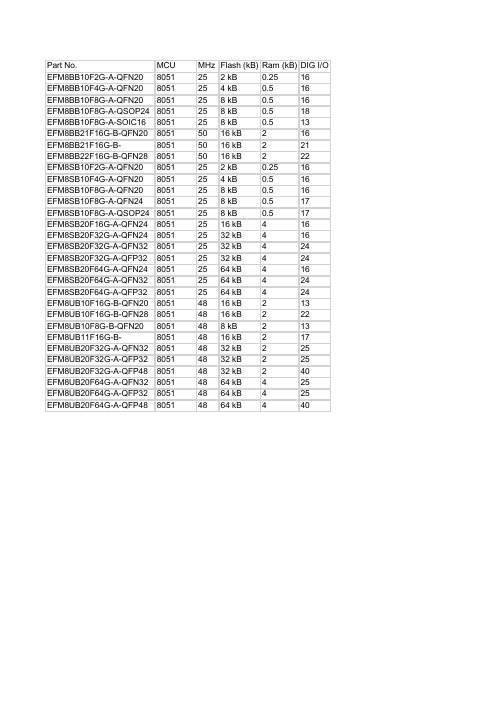
EFM8系列单片机产品选型表
25 32 kB 4
16
25 32 kB 4
24
25 32 kB 4
24
25 64 kB 4
16
25 64 kB 4
24
25 64 kB 4
24
48 16 kB 2
13
48 16 kB 2
22
48 8 kB
2
13
48 16 kB 2
17
48 32 kB 2
25
48 32 kB 2
25
48 32 kB 2
TRUE 2
TRUE 2
TRUE 2
TRUE 2
TRUE 2
TRUE 2
TRUE 2
TRUE
TRUE 2
TRUE
TRUE 2
TRUE
TRUE 2
TRUE
TRUE 2
TRUE 2
TRUE 2
TRUE 2
TRUE 2
TRUE 2
Cap Sense
TRUE TRUE TRUE TRUE TRUE
Package TQyFpNe20 QFN20 QFN20 QSOP24 SOIC16 QFN20 QSOP24 QFN28 QFN20 QFN20 QFN20 QFN24 QSOP24 QFN24 QFN24 QFN32 QFP32 QFN24 QFN32 QFP32 QFN20 QFN28 QFN20 QSOP24 QFN32 QFP32 QFP48 QFN32 QFP32 QFP48
EFM8UB20F32G-A-QFP48 8051
EFM8UB20F64G-A-QFN32 8051
EFM8UB20F64G-A-QFP32 8051
EFM8UB20F64G-A-QFP48 8051
ST 单片机选型指南

ST 意法 > STM32 微控制器STM32 (CORTEX M3)–32位微控制器STM32 32位ARM控制器概述STM32系列32位闪存微控制器基于突破性的ARM Cortex-M3 内核,这是一款专为嵌入式应用而开发的内核。
STM32系列产品得益于Cortex-M3在架构上进行的多项改进,包括提升性能的同时又提高了代码密度的Thumb-2指令集,大幅度提高的中断响应,而且所有新功能都同时具有业界最优的功耗水平。
目前ST是第一个推出基于这个内核的主要微控制器厂商。
STM32系列产品的目的是为MCU用户提供新的自由度。
它提供了一个完整的32位产品系列,在结合了高性能、低功耗和低电压特性:的同时保持了高度的集成性能和简易的开发特性:。
STM32(ARM Cortex-M3)——32位微控制器系列STM32的优势1. 搭载ARM公司最新的、具有先进架构的Cortex-M3内核2. 高级的、创新型外设3. 低功率/低电压特性:4. 最大的集成性5. 易于开发,加速了面市时间6. 整个产品系列具有脚到脚、外设和软件的高度兼容性,为您提供最大的灵活性。
STM32拥有2个完整的产品线,可以实现更多选择:1. 增强型,STM32F103的时钟频率为72MHz,具有更多的片上RAM和片上外设。
它将32位微控制器系列的性能及能效提高到一个新水平。
在72 MHz下运行的Cortex-M3内核,可以完成高端计算。
其外设集实现了超级的控制与连接性。
2. 基本型,STM32F101的时钟频率为36MHz,它是STM32系列的入门产品。
它以16位微控制器的功耗达到了32位微控制器的性能。
两个产品线都是脚到脚兼容和软件兼容,并提供了相同的嵌入式闪存存储器选项。
STM32 ,最优的平台1. STM32是您最优的平台,在这一平台上可以支持多项应用。
2. 从较少的存储及引脚要求到更大的需求3. 从要求高速运算到使用电池供电4. 从单一的成本敏感型到复杂的高价值产品整个产品系列脚到脚、外设和软件的高度兼容性为您提供完全的灵活性。
pic单片机选型 (3)

pic单片机选型1. 引言在嵌入式系统和电子设备开发中,单片机起到至关重要的作用。
它们是一种集成了中央处理器、存储器和各种输入输出接口的微型计算机芯片。
PIC(Peripheral Interface Controller)单片机是由Microchip Technology公司推出的一系列单片机产品。
选择适合的PIC单片机是一个关键的决策,它需要考虑多个方面,包括系统需求、性能要求、电源管理、成本和开发环境等因素。
本文将介绍如何进行PIC单片机选型,并对一些常用的PIC单片机进行简要的比较和评估。
2. PIC单片机选型指南2.1 系统需求在选择PIC单片机之前,首先需要明确系统的需求。
这包括但不限于以下几个方面: - 处理能力:需要考虑系统的运算复杂性和实时性要求。
如果需要处理大量数据或实时响应,可能需要选择高性能的PIC单片机。
- 存储容量:系统需要的存储容量包括程序存储器(Flash)和数据存储器(RAM)。
根据系统的功能和数据处理需求,选择合适的存储容量。
- 输入输出接口:根据系统的外部设备需求,选择具有足够的IO口和通信接口的PIC单片机。
- 电源管理:如果系统对功耗要求比较高,需要选择低功耗的PIC单片机。
- 开发环境:选择一个熟悉且易于使用的开发环境,以便开发过程更加顺利。
2.2 PIC单片机性能PIC单片机的性能指标包括但不限于以下几个方面: - 主频:PIC单片机的主频决定了其计算能力和运行速度。
主频越高,性能越强。
- 片内存储器:片内存储器包括Flash和RAM。
Flash存储程序,RAM存储变量和临时数据。
存储容量越大,可以处理的程序越复杂,数据存储越丰富。
- 片外扩展:某些应用可能需要扩展片外存储器,如外部Flash、EEPROM或SD卡。
选择具备这些扩展接口的PIC单片机可以满足更高的存储需求。
- IO口数量和类型:根据系统的外部设备需求,需要足够的IO口和通信接口。
Atmel 8051 微控制器家族 - 产品选择指南.pdf_1702133939.8143017说

Continued....Features Array•Compatible with MCS-51™ Products•4K Bytes of Reprogrammable Flash Memory–Endurance: 1,000 Write/Erase Cycles• 3.0V to 6V Operating Range•Fully Static Operation: 0 Hz to 24 MHz•Two-Level Program Memory Lock•128 x 8-Bit Internal RAM•15 Programmable I/O Lines•Two 16-Bit Timer/Counters•Six Interrupt Sources•Programmable Serial UART Channel•Direct LED Drive Outputs•On-Chip Analog Comparator•Low Power Idle and Power Down Modes•Brown-Out DetectionDescriptionThe AT89C4051 is a low-voltage, high-performance CMOS 8-bit microcomputer with 4K Bytes of Flash programmable and erasable read only memory (PEROM). The device is manufactured using Atmel’s high density nonvolatile memory technology and is compatible with the industry standard MCS-51™ instruction set. By combining a versatile 8-bit CPU with Flash on a monolithic chip, the Atmel AT89C4051 is a pow-erful microcomputer which provides a highly flexible and cost effective solution to many embedded control applications.The AT89C4051 provides the following standard features: 4K Bytes of Flash, 128 bytes of RAM, 15 I/O lines, two 16-bit timer/counters, a five vector two-level interrupt architecture, a full duplex serial port, a precision analog comparator, on-chip oscillator and clock circuitry. In addition, the AT89C4051 is designed with static logic for opera-tion down to zero frequency and supports two software-selectable power saving modes. The Idle Mode stops the CPU while allowing the RAM, timer/counters, serial port and interrupt system to continue functioning. The Power Down Mode saves the RAM contents but freezes the oscillator disabling all other chip functions until the nexthardware reset.Block DiagramAT89C4051Pin DescriptionV CCSupply voltage.GNDGround.Port 1Port 1 is an 8-bit bidirectional I/O port. Port pins P1.2 to P1.7 provide internal pullups. P1.0 and P1.1 require exter-nal pullups. P1.0 and P1.1 also serve as the positive input (AIN0) and the negative input (AIN1), respectively, of the on-chip precision analog comparator. The Port 1 output buffers can sink 20 mA and can drive LED displays directly. When 1s are written to Port 1 pins, they can be used as inputs. When pins P1.2 to P1.7 are used as inputs and are externally pulled low, they will source current (I IL) because of the internal pullups.Port 1 also receives code data during Flash programming and verification.Port 3Port 3 pins P3.0 to P3.5, P3.7 are seven bidirectional I/O pins with internal pullups. P3.6 is hard-wired as an input to the output of the on-chip comparator and is not accessible as a general purpose I/O pin. The Port 3 output buffers can sink 20 mA. When 1s are written to Port 3 pins they are pulled high by the internal pullups and can be used as inputs. As inputs, Port 3 pins that are externally being pulled low will source current (I IL) because of the pullups. Port 3 also serves the functions of various special features of the AT89C4051 as listed below:Port 3 also receives some control signals for Flash pro-gramming and verification.RSTReset input. All I/O pins are reset to 1s as soon as RST goes high. Holding the RST pin high for two machine cycles while the oscillator is running resets the device.Each machine cycle takes 12 oscillator or clock cycles. XTAL1Input to the inverting oscillator amplifier and input to the internal clock operating circuit. XTAL2Output from the inverting oscillator amplifier.Oscillator CharacteristicsXTAL1 and XTAL2 are the input and output, respectively, of an inverting amplifier which can be configured for use as an on-chip oscillator, as shown in Figure 1. Either a quartz crystal or ceramic resonator may be used. To drive the device from an external clock source, XTAL2 should be left unconnected while XTAL1 is driven as shown in Figure 2. There are no requirements on the duty cycle of the external clock signal, since the input to the internal clocking circuitry is through a divide-by-two flip-flop, but minimum and maxi-mum voltage high and low time specifications must be observed.Figure 1. Oscillator ConnectionsNote:C1, C2= 30 pF ± 10 pF for Crystals= 40 pF ± 10 pF for Ceramic Resonators Figure 2. External Clock Drive ConfigurationPort Pin Alternate FunctionsP3.0RXD (serial input port)P3.1TXD (serial output port) P3.2INT0 (external interrupt 0) P3.3INT1 (external interrupt 1) P3.4T0 (timer 0 external input) P3.5T1 (timer 1 external input)Special Function RegistersA map of the on-chip memory area called the Special Func-tion Register (SFR) space is shown in the table below. Note that not all of the addresses are occupied, and unoc-cupied addresses may not be implemented on the chip. Read accesses to these addresses will in general return random data, and write accesses will have an indetermi-nate er software should not write 1s to these unlisted loca-tions, since they may be used in future products to invoke new features. In that case, the reset or inactive values of the new bits will always be 0.Table 1. AT89C4051 SFR Map and Reset Values0F8H0FFH0F0H B000000000F7H 0E8H0EFH0E0H ACC000000000E7H 0D8H0DFH0D0H PSW000000000D7H 0C8H0CFH 0C0H0C7H0B8H IPXXX000000BFH0B0H P3111111110B7H0A8H IE0XX000000AFH 0A0H0A7H98H SCON00000000SBUFXXXXXXXX9FH90H P11111111197H88H TCON00000000TMOD00000000TL000000000TL100000000TH000000000TH1000000008FH80H SP00000111DPL00000000DPH00000000PCON0XXX000087HAT89C4051Restrictions on Certain InstructionsThe AT89C4051 is an economical and cost-effective mem-ber of Atmel’s growing family of microcontrollers. It contains 4K bytes of flash program memory. It is fully compatible with the MCS-51 architecture, and can be programmed using the MCS-51 instruction set. However, there are a few considerations one must keep in mind when utilizing certain instructions to program this device.All the instructions related to jumping or branching should be restricted such that the destination address falls within the physical program memory space of the device, which is 4K for the AT89C4051. This should be the responsibility of the software programmer. For example, LJMP 0FE0H would be a valid instruction for the AT89C4051 (with 4K of memory), whereas LJMP 1000H would not.1. Branching instructions:LCALL, LJMP, ACALL, AJMP, SJMP, JMP @A+DPTR These unconditional branching instructions will execute correctly as long as the programmer keeps in mind that the destination branching address must fall within the physical boundaries of the program memory size (locations 00H to FFFH for the 89C4051). Violating the physical space limits may cause unknown program behavior.CJNE [...], DJNZ [...], JB, JNB, JC, JNC, JBC, JZ, JNZ With these conditional branching instructions the same rule above applies. Again, violating the memory boundaries may cause erratic execution.For applications involving interrupts the normal interrupt service routine address locations of the 80C51 family archi-tecture have been preserved.2. MOVX-related instructions, Data Memory:The AT89C4051 contains 128 bytes of internal data mem-ory. Thus, in the AT89C4051 the stack depth is limited to 128 bytes, the amount of available RAM. External DATA memory access is not supported in this device, nor is exter-nal PROGRAM memory execution. Therefore, no MOVX [...] instructions should be included in the program.A typical 80C51 assembler will still assemble instructions, even if they are written in violation of the restrictions men-tioned above. It is the responsibility of the controller user to know the physical features and limitations of the device being used and adjust the instructions used correspond-ingly.Program Memory Lock BitsOn the chip are two lock bits which can be left unpro-grammed (U) or can be programmed (P) to obtain the addi-tional features listed in the table below:Lock Bit Protection Modes(1)Note: 1.The Lock Bits can only be erased with the Chip Erase operation.Idle ModeIn idle mode, the CPU puts itself to sleep while all the on-chip peripherals remain active. The mode is invoked by software. The content of the on-chip RAM and all the spe-cial functions registers remain unchanged during this mode. The idle mode can be terminated by any enabled interrupt or by a hardware reset.P1.0 and P1.1 should be set to ’0’ if no external pullups are used, or set to ’1’ if external pullups are used.It should be noted that when idle is terminated by a hard-ware reset, the device normally resumes program execu-tion, from where it left off, up to two machine cycles before the internal reset algorithm takes control. On-chip hardware inhibits access to internal RAM in this event, but access to the port pins is not inhibited. To eliminate the possibility of an unexpected write to a port pin when Idle is terminated by reset, the instruction following the one that invokes Idle should not be one that writes to a port pin or to external memory.Power Down ModeIn the power down mode the oscillator is stopped, and the instruction that invokes power down is the last instruction executed. The on-chip RAM and Special Function Regis-ters retain their values until the power down mode is termi-nated. The only exit from power down is a hardware reset. Reset redefines the SFRs but does not change the on-chip RAM. The reset should not be activated before V CC is restored to its normal operating level and must be held active long enough to allow the oscillator to restart and sta-bilize.P1.0 and P1.1 should be set to ’0’ if no external pullups are used, or set to ’1’ if external pullups are used.Program Lock BitsLB1LB2Protection Type1U U No program lock features.2P U Further programming of the Flashis disabled.3P P Same as mode 2, also verify isdisabled.Brown-Out DetectionWhen V CC drops below the detection threshold, all port pins (except P1.0 and P1.1) are weakly pulled high. When V CC goes back up again, an internal Reset is automatically generated after a delay of typically 15 msec. The nominal brown-out detection threshold is 2.3V ± 10%.Programming The FlashThe AT89C4051 is shipped with the 4K bytes of on-chip PEROM code memory array in the erased state (i.e., con-tents = FFH) and ready to be programmed. The code mem-ory array is programmed one byte at a time. Once the array is programmed, to re-program any non-blank byte, the entire memory array needs to be erased electrically. Internal Address Counter: The AT89C4051 contains an internal PEROM address counter which is always reset to 000H on the rising edge of RST and is advanced by apply-ing a positive going pulse to pin XTAL1.Programming Algorithm: To program the AT89C4051, the following sequence is recommended.1.Power-up sequence:Apply power between V CC and GND pinsSet RST and XTAL1 to GND2.Set pin RST to ’H’Set pin P3.2 to ’H’3.Apply the appropriate combination of ’H’ or ’L’ logiclevels to pins P3.3, P3.4, P3.5, P3.7 to select one of the programming operations shown in the PEROM Pro-gramming Modes table.To Program and Verify the Array:4.Apply data for Code byte at location 000H to P1.0 toP1.7.5.Raise RST to 12V to enable programming.6.Pulse P3.2 once to program a byte in the PEROM arrayor the lock bits. The byte-write cycle is self-timed and typically takes 1.2 ms.7.To verify the programmed data, lower RST from 12V tologic ’H’ level and set pins P3.3 to P3.7 to the appropriate levels. Output data can be read at the port P1 pins.8.To program a byte at the next address location, pulseXTAL1 pin once to advance the internal address counter.Apply new data to the port P1 pins.9.Repeat steps 5 through 8, changing data and advancingthe address counter for the entire 4K bytes array or until the end of the object file is reached.10.Power-off sequence:set XTAL1 to ’L’set RST to ’L’Turn V CC power offData Polling: The AT89C4051 features Data Polling to indicate the end of a write cycle. During a write cycle, an attempted read of the last byte written will result in the com-plement of the written data on P1.7. Once the write cycle has been completed, true data is valid on all outputs, and the next cycle may begin. Data Polling may begin any time after a write cycle has been initiated.Ready/Busy: The Progress of byte programming can also be monitored by the RDY/BSY output signal. Pin P3.1 is pulled low after P3.2 goes High during programming to indi-cate BUSY. P3.1 is pulled High again when programming is done to indicate READY.Program Verify: If lock bits LB1 and LB2 have not been programmed code data can be read back via the data lines for verification:1.Reset the internal address counter to 000H by bringingRST from ’L’ to ’H’.2.Apply the appropriate control signals for Read Code dataand read the output data at the port P1 pins.3.Pulse pin XTAL1 once to advance the internal addresscounter.4.Read the next code data byte at the port P1 pins.5.Repeat steps 3 and 4 until the entire array is read.The lock bits cannot be verified directly. Verification of the lock bits is achieved by observing that their features are enabled.Chip Erase: The entire PEROM array (4K bytes) and the two Lock Bits are erased electrically by using the proper combination of control signals and by holding P3.2 low for 10 ms. The code array is written with all “1”s in the Chip Erase operation and must be executed before any non-blank memory byte can be re-programmed.AT89C4051Reading the Signature Bytes: The signature bytes are read by the same procedure as a normal verification of locations 000H, 001H, and 002H, except that P3.5 and P3.7 must be pulled to a logic low. The values returned are as follows.(000H) = 1EH indicates manufactured by Atmel (001H) = 41H indicates 89C4051Programming InterfaceEvery code byte in the Flash array can be written and the entire array can be erased by using the appropriate combi-nation of control signals. The write operation cycle is self-timed and once initiated, will automatically time itself to completion.All major programming vendors offer worldwide support for the Atmel microcontroller series. Please contact your local programming vendor for the appropriate software revision.Flash Programming ModesNotes:1.The internal PEROM address counter is reset to 000H on the rising edge of RST and is advanced by a positive pulse atXT AL 1 pin.2.Chip Erase requires a 10-ms PROG pulse.3.P3.1 is pulled Low during programming to indicate RDY/BSY .ModeRST/VPP P3.2/PROGP3.3P3.4P3.5P3.7Write Code Data (1)(3)12VLHHHRead Code Data (1)H H L L H H Write LockBit - 112VHHHHBit - 212V H H L LChip Erase 12VH L L LRead Signature Byte H H L L L L(2)Figure 3. Programming the Flash MemoryFigure 4. Verifying the Flash MemoryFlash Programming and Verification CharacteristicsT A = 0°C to 70°C, V CC = 5.0 ± 10%Note:1. Only used in 12-volt programming mode.Symbol ParameterMin Max Units V PP Programming Enable Voltage 11.512.5V I PP Programming Enable Current 250µA t DVGL Data Setup to PROG Low 1.0µs t GHDX Data Hold After PROG 1.0µs t EHSH P3.4 (ENABLE) High to V PP 1.0µs t SHGL V PP Setup to PROG Low 10µs t GHSL V PP Hold After PROG 10µs t GLGH PROG Width1110µs t ELQV ENABLE Low to Data Valid 1.0µs t EHQZ Data Float After ENABLE 0 1.0µs t GHBL PROG High to BUSY Low 50ns t WC Byte Write Cycle Time2.0ms t BHIH RDY/BSY\ to Increment Clock Delay1.0µs t IHIL Increment Clock High200nsAT89C4051Flash Programming and Verification WaveformsAbsolute Maximum Ratings*Operating Temperature.................................-55°C to +125°C *NOTICE:Stresses beyond those listed under “Absolute Maximum Ratings” may cause permanent dam-age to the device. This is a stress rating only and functional operation of the device at these or any other conditions beyond those indicated in the operational sections of this specification is not implied. Exposure to absolute maximum rating conditions for extended periods may affect device reliability.Storage T emperature.....................................-65°C to +150°C Voltage on Any Pinwith Respect to Ground.....................................-1.0V to +7.0V Maximum Operating Voltage.............................................6.6V DC Output Current......................................................25.0 mADC CharacteristicsT A = -40°C to 85°C, V CC = 3.0V to 6.0V (unless otherwise noted)Notes:1.Under steady state (non-transient) conditions, I OL must be externally limited as follows:Maximum I OL per port pin: 20 mAMaximum total I OL for all output pins: 80 mAIf I OL exceeds the test condition, V OL may exceed the related specification. Pins are not guaranteed to sink current greater than the listed test conditions.2.Minimum V CC for Power Down is 2V .Symbol Parameter ConditionMin Max Units V IL Input Low Voltage -0.50.2 V CC - 0.1V V IH Input High Voltage (Except XT AL1, RST)0.2 V CC + 0.9V CC + 0.5V V IH1Input High Voltage (XT AL1, RST)0.7 V CCV CC + 0.5V V OL Output Low Voltage (1)(Ports 1, 3)I OL = 20 mA, V CC = 5V I OL = 10 mA, V CC = 2.7V 0.5V V OHOutput High Voltage (Ports 1, 3)I OH = -80 µA, V CC = 5V ± 10% 2.4V I OH = -30 µA 0.75 V CCV I OH = -12 µA0.9 V CCVI IL Logical 0 Input Current (Ports 1, 3)V IN = 0.45V-50µA I TL Logical 1 to 0 T ransition Current (Ports 1, 3)V IN = 2V , V CC = 5V ± 10%-750µA I LI Input Leakage Current (Port P1.0, P1.1)0 < V IN < V CC ±10µA V OS Comparator Input Offset Voltage V CC = 5V20mV V CM Comparator Input Common Mode Voltage0V CC V RRST Reset Pulldown Resistor 50300K ΩC IO Pin Capacitance T est Freq. = 1 MHz, T A = 25°C 10pF I CCPower Supply CurrentActive Mode, 12 MHz, V CC = 6V/3V 15/5.5mA Idle Mode, 12 MHz, V CC = 6V/3V P1.0 & P1.1 = 0V or V CC5/1mA Power Down Mode (2)V CC = 6V P1.0 & P1.1 = 0V or V CC 100µA V CC = 3V P1.0 & P1.1 = 0V or V CC20µAExternal Clock Drive WaveformsExternal Clock DriveSymbol Parameter V CC = 3.0V to 6.0V V CC = 4.0V to 6.0V UnitsMin Max Min Max1/t CLCL Oscillator Frequency012024MHz t CLCL Clock Period83.341.6ns t CHCX High Time3015ns t CLCX Low Time3015ns t CLCH Rise Time2020ns t CHCL Fall Time2020nsSerial Port Timing: Shift Register Mode Test Conditions(V CC = 5.0V ± 20%; Load Capacitance = 80 pF)Shift Register Mode Timing WaveformsSymbolParameter12 MHz Osc Variable Oscillator UnitsMinMaxMin Maxt XLXL Serial Port Clock Cycle Time1.012t CLCL µs t QVXH Output Data Setup to Clock Rising Edge 70010t CLCL -133ns t XHQX Output Data Hold After Clock Rising Edge 502t CLCL -117ns t XHDX Input Data Hold After Clock Rising Edge 0ns t XHDVClock Rising Edge to Input Data Valid70010t CLCL -133nsAC Testing Input/Output Waveforms (1)Note: 1.AC Inputs during testing are driven at V CC - 0.5V for a logic 1 and 0.45V for a logic 0. Timing measure-ments are made at V IH min. for a logic 1 and V IL max. for a logic 0.Float Waveforms (1)Note: 1.For timing purposes, a port pin is no longer float-ing when a 100 mV change from load voltage occurs. A port pin begins to float when 100 mV change frothe loaded V OH /V OLlevel occurs.Notes: 1.XT AL1 tied to GND for I CC (power down)2.P.1.0 and P1.1 = V CC or GND3.Lock bits programmedOrdering InformationSpeed (MHz)PowerSupply Ordering Code Package Operation Range12 3.0V to 6.0V A T89C4051-12PCA T89C4051-12SC 20P320SCommercial(0°C to 70°C)A T89C4051-12PI A T89C4051-12SI 20P320SIndustrial(-40°C to 85°C)A T89C4051-12P A A T89C4051-12SA 20P320SAutomotive(-40°C to 105°C)24 4.0V to 6.0V A T89C4051-24PCA T89C4051-24SC 20P320SCommercial(0°C to 70°C)A T89C4051-24PI A T89C4051-24SI20P320SIndustrial(-40°C to 85°C) Package Type20P320 Lead, 0.300” Wide, Plastic Dual In-line Package (PDIP)20S20 Lead, 0.300” Wide, Plastic Gull Wing Small Outline (SOIC)AT89C4051 Packaging Information。
PHILIPS32位单片机选型指南

LPC210664K128K Y Y4Y Y Y2Y Y32 1.8V 3.3V60LQFP48 LPC210532K128K Y Y4Y Y Y2Y Y32 1.8V 3.3V60LQFP48 LPC210416K128K Y Y4Y Y Y2Y Y32 1.8V 3.3V60LQFP48
特性
向量中断控制器
PHILIPS 32位单片机选型指南
管脚图
LPC2100系列是PHILIPS推出的以ARM7TDMI-S 处理器为内核的32位单片机典型应用于电子收款机
机顶盒STB保安系统串行协议转换器自动售货机医疗系统等
Flash编程时间1ms可编程512字节扇区擦除和整片擦除只需400ms
最多可达64K静态RAM
外设功能可单独使能/禁止实现功耗最优化
两个低功耗模式空闲和掉电
通过外部中断将处理器从掉电模式中唤醒
仿真跟踪模块支持实时跟踪
标准ARM测试/调试接口兼容现有工具
双UART其中一个带有完全的调制解调器接口
高速I2C串行接口(400kb/s)
功能图。
选型手册V20130217

立足本土,作国内最杰出最用心的MCU设计公司GPIO 通用型MCU芯片型号可编程只读存储器随机存储器EEPROM工作电压(伏)内部振荡器(赫兹)外部振荡器(赫兹)系统时钟I/O端口+Input脉宽调制中断源定时器工作电流待机电流看门狗定时器低电压复位工作温度封装型式其他Part Number ROM RAM EEPROMVoltage(V)InternalOscillator(HZ)ExternalOscillator(HZ)Fsys I/O +IN PWMInterruptSourceTimerOperatingCurrentIdleCurrentWDT LVROperatingTemp.PKG Type OtherMC20P011Kx8Bit64×8Bit/ 2.0~5.52M/4M/8M±2%400K~8M2T11/5+11CH8Bit62/8Bit3mA/4M<1uA yes2.1V3.6V-40~85℃DIP/SOP14/8与义隆153S和松翰8P2501B脚位兼容。
具有硬件Buzzer输出端口MC20E011Kx8Bit64×8Bit 256x8Bit2.0~5.52M/4M/8M±2%400K~8M2T11/5+11CH8Bit62/8Bit3mA/4M<1uA yes2.1V3.6V-40~85℃DIP/SOP16/8用MCP技术把一颗EEPROM(24C02)封装进去,E2ROM是串行通讯,占去2个IO口MC20P02B2Kx8Bit64×8Bit/ 2.0~5.52M/4M/8M±2%400K~8M2T17/15/13/11/5+1/51/8Bit3mA/4M<1uA yes2.1V3.6V-40~85℃DIP/SOP20/18/16/14/818pin与中颖69P20C,松翰8P2612,义隆78P156脚位兼容20pin与松翰8P2613脚位兼容MC20E02B2Kx8Bit64×8Bit 256x8Bit2.0~5.52M/4M/8M±2%400K~8M2T11/9+1/51/8Bit3mA/4M<1uA yes2.1V3.6V-40~85℃DIP/SOP 16用MCP技术把一颗EEPROM(24C02)封装进去,E2ROM是串行通讯,占去2个IO口MC20P044K×8Bit128×8Bit/ 2.0~5.52M/4M/8M±2%400K~8M2T17/15/13+1/51/8Bit3mA/4M<1uA yes2.1V3.6V-40~85℃DIP/SOP20/18/1618pin与中颖69P20C,松翰8P2612,义隆78P156脚位兼容20pin与松翰8P2613脚位兼容具有2路比较器(可软件修调偏置)MC20P8011Kx8Bit64×8Bit/ 2.0~5.51M/2M/4M/8M±2%/2T5/3+11CH8Bit42/8Bit3mA/4M<1uA yes2.1V3.6V-40~85℃DIP/SOP8SOT23-6TSSOP8VPP可作输入/开漏输出SOT23-6封装可直接烧写MC30P011Kx14Bit48×8Bit/ 2.0~5.51M/2M/4M/8M/455K±1.5%32K500~20M2T4T11/5/3+11CH8Bit42/8Bit1mA/4M<1uA yes1.5V3.6V7级可选-40~85℃DIP/SOP14/8管脚和程序全面兼容AM8EB153XFM8PS53,EM78P153,仅管脚和兼容SN8P2501B☆MC30P022Kx16Bit64×8Bit/ 2.0~5.51M/2M/4M/8M/455K±1.5%32K500~20M2T4T17/15/13+1243/8Bit1mA/4M<1uA yes1.5V3.6V7级可选40~85℃DIP/SOP20/18/1618pin与中颖69P20C,松翰8P2612,义隆78P156脚位兼容20pin与松翰8P2613脚位兼容具有2路比较器(可软件修调偏置)*拥有更佳的RAM掉电保持功能:只要芯片的VDD和GND之间电压维持在0.7V以上时,RAM数据就可以一直保持,正常情况下断电后依靠外挂电容即可以保持RAM数据24小时以上。
- 1、下载文档前请自行甄别文档内容的完整性,平台不提供额外的编辑、内容补充、找答案等附加服务。
- 2、"仅部分预览"的文档,不可在线预览部分如存在完整性等问题,可反馈申请退款(可完整预览的文档不适用该条件!)。
- 3、如文档侵犯您的权益,请联系客服反馈,我们会尽快为您处理(人工客服工作时间:9:00-18:30)。
XTAL1/P3.1 2
16字节可擦除页规格。
CLKOUT/XTAL2/P3.0 3
● 2个16位定时/计数器(LPC901的定时器0可作为PWM输出)。 ● 模拟比较器:2个(LPC902/903/904),1个(LPC901)。
RST/P1.5 4
● 2路输入的A/D转换器/1个DAC输出,可选择参考源(LPC904)。
功能部件 UART,RTC,KBI
ADC/DAC CMP PWM
128B
8脚
1K
功能部件 UART,RTC,KBI
ADC/DAC CMP PWM
SPI、I2C
16脚 14脚
256B 2K 1K 128B
功能部件 UART,RTC,KBI
ADC/DAC CMP PWM
SPI、I2C ISP
8K 4K 256B 20脚 2K
在程序运行时改变代码。 ● 64脚LQFP封装。 ● DP-9401开发套件。
智能卡水表 / 气表“单片”解决方案
P89LPC9102/9103/9107 Flash单片机
04 ● 128字节 RAM数据存储器。1kB可字节擦除的Flash程 序存储器,组成256字节扇区和16字节擦除页规格。
13 P0.2/CIN2A/KBI2 12 P0.4/CIN1A/KBI4 11 P0.5/CMPREF/KBI5 10 VDD
9 P1.0/TXD
8 CLKOUT/XTAL2/P3.0
P2.2/MOSI 1 SPICLK/P2.5 2
● Flash保密位可防止程序被读出。 ● 在应用中编程(IAP-Lite)和字节擦写功能使得程序存储器可用于非易
失性数据的存储。 ● 实时时钟可作为系统定时器。 ● 2个模拟比较器。可选择输入和参考源。 ● SPI通信端口、4个键盘中断输入。 ● 选择片内振荡和片内复位时可多达12个I/O口。 ● 14脚TSSOP和DIP封装。
TSSOP封装(P89LPC9107)。
2
http://www.zlgmcu.com
R
周立功单片机
专注的力量成就梦想
P89LPC901/902/903 Flash单片机
● 2个(LPC901)/3个(LPC903/904)/5个(LPC902)键盘中断输入。
VDD 1
● 128字节RAM数据存储器。1KB Flash程序存储器,具有256字节可擦除扇区、
● 2个16位定时/计数器(P89LPC907的定时器0可作为一个PWM输出)。 ● 只有一个模拟比较器,可选择参考源。 ● 选择片内振荡和片内复位时可多达6个I/O口。 ● 增强型UART。具有波特率发生器、间隔、帧错误检测、自动地址识别
和通用的中断功能(LPC906除外)。 ● 23位的系统定时器,可用作实时时钟。 ● 高精度的内部RC振荡器(7.3728MHz)。 ● 8脚SO/DIP封装。 ● 工作温度:-40~85℃。
专门定制的单片机
VDD
R≤
tr 2CB
LPC931
MICRO- CONTROLLER
VSS 20PIN单片机
LPC9401
SDA SCL OSC
VDD VLCD PCF8576D
32 segment drives LCD Panel
Upto
4 backplanes
128 segments
A0 A1 A2 Sa0 VSS
http://www.zlgmcu.com
RST/P1.5 1 Vss 2
P0.6/CMP1/KBI6 3 XTAL1/P3.1 4
8
LPC906 7 6
5
P0.4/CIN1A/KBI4 P0.5/CMPREF/KBI5 VDD CLKOUT/XTAL2/P3.0
RST/P1.5 1
8 P0.4/CIN1A/KBI4
● 利用商用编程器可简单实现串行Flash在电路编程(ICP)。 Flash保密位可防止敏感应用程序被读出。
● 4个中断优先级。 ● 2个键盘中断输入。 ● 双数据指针。 ● 外部时钟输入。时钟输出(P89LPC9102/9107)。 ● 极小的10脚HVSON封装(LPC9102/9103)。14脚
PHILIPS 微控制器领导品牌
PHILIPS单片机选型指南
LPC900系列 LPC700系列 80C51系列
R
周立功单片机
02
用增强型LPC900系列Flash单片机设计可靠的产品
●● 单 内字置L节RPT读CC写实9功0时0能时与确钟众保功内能不部部同F件l的ash优可势用作E2 PROM
P89LPC912/913/914 Flash单片机
● 128字节 RAM数据存储器。1KB Flash程序存储器,具有256字节可 擦除扇区和16字节擦除页规格。
● 2个16位定时/计数器,每一个定时器均可设置为溢出时触发相应端口 输出或作为PWM输出。
● 串行Flash在电路编程(ICP)允许利用商用EPROM编程器实现简单代 码的编程。
★ 丰富的片内外围资源:WDT,UART,I2C,SPI, D/A, E2PROM, RTC,A/D,比较器,CCU,掉电检测等;
★ 内置高精度RC振荡器:标称频率7.3728MHz,精度 可达1%;
★ 超小型TSSOP封装(另有DIP、PLCC封装),能最 大限度节省电路板面积;
★ 超低功耗:支持低速晶振,3级省电模式,典型掉电 电流仅1μA;
● 单个字节擦除功能允许Flash程序存储器的任何字节 可用作非易失性数据存储。
● 2个16位定时/计数器。 ● 可用作RTC的23位系统定时器。 ● 4路输入的8位A/D转换器/单个DAC输出。带有一个可
选择参考源的模拟比较器。 ● 增强型UART。具有波特率发生器、间隔检测、帧错
VDD 1
● 选择片内振荡和片内复位时可多达6个I/O口。
P0.2/CIN2A/KBI2 2
● 操作电压VDD范围为2.4~3.6V。I/O口可承受5V(可上拉或驱动到5.5V)。 ● 增强型UART。具有波特率发生器、间隔、帧错误检测、自动地址识别和通用
P0.0/CMP2/KBI0 3 RST/P1.5 4
误检测、自动地址检测和通用中断功能 (P89LPC9103/9107)。 ● 高精度内部RC振荡器选项,出厂校准精度为1,操 作时不需要外接振荡器件。可选择RC振荡器选项并且 其频率可进行很好的调节。 ● VDD操作电压范围为2.4~3.6V,I/O口可承受5V(可上 拉或驱动到5.5V)。 ● 当使用片内振荡器和复位选项时,I/O口可高达10个 (LPC9107)和8个(LPC9102/9103)。 ● 当在时钟倍频模式下使用内部7.3728MHz 的RC振荡 器时,除乘法和除法指令外,CPU的指令执行时间为 136 ̄272ns。只需要较低的时钟频率即可达到同样的 性能,这无疑降低了功耗和EMI。
★ 在线ICP编程,仅需引出5根线(VCC, GND, RST, P0.4, P0.5);
★ Flash存储器:容量1~16KB,具有ISP、IAP功能, 03 可以当作E2PROM使用;
★ 工业级产品,抗干扰能力强,操作电压2.4~3.6V, 管脚数8~44,I/O可兼容5V逻辑。
从小型封装到功能齐全的一系列产品
P1.1/RxD 3 RST/P1.5 4
8 7 LPC901 6 5
8 7 LPC902 6 5
8 7 LPC903 6 5
VSS P0.4/CIN1A/KBI4 P0.5/CMPREF/KBI5 P1.2/T0
VSS P0.4/CIN1A/KBI4 P0.5/CMPREF/KBI5 P0.6/CMPI/KBI6
P89LPC9401FBD
PCF8563T 改进后
CAT24WC16 LCD驱动器
● 通过IAP在线编程,内部Flash可用作 E2PROM。
● 8kB Flash程序存储器,具有1kB可擦除扇区和 64字节可擦除页规格。
● 内置RTC实时时钟功能部件。 ● 32×4段LCD驱动器。 ● 256字节 RAM数据存储器。 ● 2个模拟比较器。可选择输入和参考源。 ● 字节方式I2C,速率可达400kHz。 ● 8个键盘中断输入,2路外部中断输入。 ● 4个中断优先级。 ● Flash程序存储器可实现在应用中编程,这允许
键盘中断
看门狗 定时器
可编程时钟 分频
CPU时钟
模拟比较器 CCU
定时器1/2 RTC定时器
晶体或 谐振器
可配置振荡器
片内RC振荡器
电源监控 上电复位/掉电检测
★ 80C51体系结构:如果您用过8051内核的单片机就 很容易入门;
★ 超高速CPU内核:18MHz的LPC900相当于 108MHz的传统80C51;
LPC90X
LPC91X
LPC92X
http://www.zlgmcu.com
功能部件 UART,RTC,KBI
ADC/DAC CMP PWM
SPI、I2C ISP CCU
引脚数目
FLASH 容量
RAM 容量
16K 768B 8K 8脚 4K 256B
LPC93X
R
周立功单片机
专注的力量成就梦想
内置LCD驱动器的P89LPC9401 Flash单片机
XTAL1/P3.1 7
14 P2.3/MISO
LPC 912
LPC 912
13 P0.2/CIN2A/KBI2 12 P0.4/CIN1A/KBI4 11 P0.5/CMPREF/KBI5 10 VDD
9 P2.4/SS
8 CLKOUT/XTAL2/P3.0
14 P2.3/MISO
LPC 913
LPC 913
VSS P0.4/CIN1A/KBI4 P0.5/CMPREF/KBI5 P1.0/TXD