MAX3762EEP中文资料
MAX471MAX472的中文资料大全
M A X471M A X472的中文资料大全(总4页)-本页仅作为预览文档封面,使用时请删除本页-MAX471/MAX472的特点、功能美国美信公司生产的精密高端电流检测放大器是一个系列化产品,有MAX471/MA X472、 MAX4172/MAX4173等。
它们均有一个电流输出端,可以用一个电阻来简单地实现以地为参考点的电流/电压的转换,并可工作在较宽电压内。
MAX471/MAX472具有如下特点:●具有完美的高端电流检测功能;●内含精密的内部检测电阻(MAX471);●在工作温度范围内,其精度为2%;●具有双向检测指示,可监控充电和放电状态;●内部检测电阻和检测能力为3A,并联使用时还可扩大检测电流范围;●使用外部检测电阻可任意扩展检测电流范围(MAX472);●最大电源电流为100μA;●关闭方式时的电流仅为5μA;●电压范围为3~36V;●采用8脚DIP/SO/STO三种封装形式。
MAX471/MAX472的引脚排列如图1所示,图2所示为其内部功能框图。
表1为MAX471/MAX472的引脚功能说明。
MAX471的电流增益比已预设为500μA/A,由于2kΩ的输出电阻(ROUT)可产生1V/A的转换,因此±3A时的满度值为3V.用不同的ROUT电阻可设置不同的满度电压。
但对于MAX471,其输出电压不应大于VRS+。
对于MAX472,则不能大于。
MAX471引脚图如图1所示,MAX472引脚图如图2所示。
MAX471/MAX472的引脚功能说明引脚名称功能MAX471MAX47211SHDN关闭端。
正常运用时连接到地。
当此端接高电平时,电源电流小于5μA2,3-RS+内部电流检测电阻电池(或电源端)。
“+”仅指示与SIGN输出有关的流动方向。
封装时已将2和3连在了一起-2空脚-3RG1增益电阻端。
通过增益设置电阻连接到电流检测电阻的电池端44GND地或电池负端55SIGN集电极开路逻辑输出端。
MAX3232ECPE中文资料
MAX3222EEPN -40°C to +85°C 18 Plastic DIP —
MAX3232ECAE 0°C to +70°C 16 SSOP
—
MAX3232ECWE 0°C to +70°C 16 Wide SO —
MAX3232ECPE 0°C to +70°C 16 Plastic DIP —
Next-Generation Device Features
♦ For Space-Constrained Applications MAX3228E/MAX3229E: ±15kV ESD-Protected, +2.5V to +5.5V, RS-232 Transceivers in UCSP
*Dice are tested at TA = +25°C, DC parameters only. **EP = Exposed paddle.
Ordering Information continued at end of data sheet.
Pin Configurations, Selector Guide, and Typical Operating Circuits appear at end of data sheet.
MAX3222EETP
20 Thin QFN-40°C to +85°C EP** (5mm x
5mm)
T2055-5
MAX3222EEUP -40°C to +85°C 20 TSSOP
—
MAX3222EEAP -40°C to +85°C 20 SSOP
—
MAX3222EEWN -40°C to +85°C 18 Wide SO —
SP202EEP中文资料
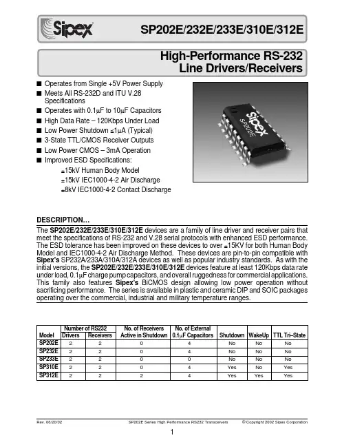
■Operates from Single +5V Power Supply ■Meets All RS-232D and ITU V.28Specifications■Operates with 0.1µF to 10µF Capacitors ■High Data Rate – 120Kbps Under Load ■Low Power Shutdown ≤1µA (Typical)■3-State TTL/CMOS Receiver Outputs ■Low Power CMOS – 3mA Operation ■Improved ESD Specifications:±15kV Human Body Model±15kV IEC1000-4-2 Air Discharge ±8kV IEC1000-4-2 Contact DischargeDESCRIPTION…The SP202E/232E/233E/310E/312E devices are a family of line driver and receiver pairs that meet the specifications of RS-232 and V.28 serial protocols with enhanced ESD performance.The ESD tolerance has been improved on these devices to over ±15KV for both Human Body Model and IEC1000-4-2 Air Discharge Method. These devices are pin-to-pin compatible with Sipex's SP232A/233A/310A/312A devices as well as popular industry standards. As with the initial versions, the SP202E/232E/233E/310E/312E devices feature at least 120Kbps data rate under load, 0.1µF charge pump capacitors, and overall ruggedness for commercial applications.This family also features Sipex's BiCMOS design allowing low power operation without sacrificing performance. The series is available in plastic and ceramic DIP and SOIC packages operating over the commercial, industrial and military temperature ranges.Number of RS232No. of Receivers No. of ExternalModel Drivers Receivers Active in Shutdown 0.1µF CapacitorsShutdown WakeUp TTL Tri–StateSP202E 2204No No No SP232E 2204No No No SP233E 2200No No No SP310E 2204Yes No Yes SP312E2224Yes Yes YesABSOLUTE MAXIMUM RATINGS This is a stress rating only and functional operation of the device at these or any other conditions above those indicated in the operation sections of this specification is not implied. Exposure to absolute maximum rating conditions for extended periods of time may affect reliability.Vcc .................................................................................................................................................................+6VV+....................................................................................................................(Vcc-0.3V) to +11.0V V-............................................................................................................................................................-11.0V Input VoltagesT IN .........................................................................................................................-0.3 to (Vcc +0.3V)RIN ............................................................................................................................................................±15VOutput VoltagesT OUT ....................................................................................................(V+, +0.3V) to (V-, -0.3V)ROUT ................................................................................................................-0.3V to (Vcc +0.3V)Short Circuit DurationT OUT .........................................................................................................................................ContinuousPower DissipationCERDIP..............................................................................675mW(derate 9.5mW/°C above +70°C)Plastic DIP..........................................................................375mW(derate 7mW/°C above +70°C)Small Outline......................................................................375mW(derate 7mW/°C above +70°C)SPECIFICATIONS元器件交易网元器件交易网PERFORMANCE CURVES+Figure 1. Typical Circuit using the SP202E or SP232E.FEATURES…The SP202E/232E/233E/310E/312E devices are a family of line driver and receiver pairs that meet the specifications of RS-232 and V.28serial protocols with enhanced ESD perfor-mance. The ESD tolerance has been improved on these devices to over ±15KV for both Human Body Model and IEC1000-4-2 Air Discharge Method. These devices are pin-to-pin compat-ible with Sipex's 232A/233A/310A/312A devices as well as popular industry standards.As with the initial versions, the SP202E/232E/233E/310E/312E devices feature10V/µs slew rate, 120Kbps data rate under load, 0.1µF charge pump capacitors, overall ruggedness for commercial applications, and increased drive current for longer and more flexible cable configurations. This family also features Sipex's BiCMOS design allowing low power operation without sacrificing performance.The SP202E/232E/233E/310E/312E devices have internal charge pump voltage converters which allow them to operate from a single +5V supply. The charge pumps will operate with polarized or non-polarized capacitors ranging from 0.1 to 10 µF and will generate the ±10V needed to generate the RS-232 output levels.Both meet all EIA RS-232 and ITU V.28specifications.The SP310E provides identical features as the SP232E with a single control line which simultaneously shuts down the internal DC/DC converter and puts all transmitter and receiver outputs into a high impedance state. The SP312E is identical to the SP310E with separate tri-state and shutdown control lines.THEORY OF OPERATIONThe SP232E , SP233E , SP310E and SP312Edevices are made up of three basic circuit blocks –1) a driver/transmitter, 2) a receiver and 3) a charge pump. Each block is described below.Driver/TransmitterThe drivers are inverting transmitters, which ac-cept TTL or CMOS inputs and output the RS-232signals with an inverted sense relative to the input logic levels. Typically the RS-232 output voltage swing is ±9V. Even under worst case loading conditions of 3kOhms and 2500pF, the output is guaranteed to be ±5V, which is consistent with the RS-232 standard specifications. The transmitter outputs are protected against infinite short-circuits to ground without degradation in reliability.元器件交易网The instantaneous slew rate of the transmitteroutput is internally limited to a maximum of 30V/µs in order to meet the standards [EIA RS-232-D 2.1.7, Paragraph (5)]. However, the transition re-gion slew rate of these enhanced products is typi-cally 10V/µs. The smooth transition of the loaded output from V OL to V OH clearly meets the mono-tonicity requirements of the standard [EIA RS-232-D 2.1.7, Paragraphs (1) & (2)].ReceiversThe receivers convert RS-232 input signals to inverted TTL signals. Since the input is usually from a transmission line, where long cable lengthsand system interference can degrade the signal, theinputs have a typical hysteresis margin of 500mV.This ensures that the receiver is virtually immune to noisy transmission lines.The input thresholds are 0.8V minimum and 2.4V maximum, again well within the ±3V RS-232requirements. The receiver inputs are also pro-tected against voltages up to ±15V. Should an input be left unconnected, a 5KOhm pulldown resistor to ground will commit the output of the receiver to a high state.Figure 2. Typical Circuits using the SP233ECP and SP233ECTFigure 3. Typical Circuits using the SP310E and SP312EFigure 4. Charge Pump — Phase 1Figure 5. Charge Pump — Phase 2In actual system applications, it is quite possible for signals to be applied to the receiver inputs before power is applied to the receiver circuitry.This occurs, for example, when a PC user attempts to print, only to realize the printer wasn’t turned on.In this case an RS-232 signal from the PC will appear on the receiver input at the printer. When the printer power is turned on, the receiver will operate normally. All of these enhanced devices are fully protected.Charge PumpThe charge pump is a Sipex –patented design (5,306,954) and uses a unique approach com-pared to older less–efficient designs. The charge pump still requires four external capacitors, but uses a four–phase voltage shifting technique to attain symmetrical 10V power supplies. There is a free–running oscillator that controls the four phases of the voltage shifting. A description of each phase follows.Phase 1— V SS charge storage —During this phase of the clock cycle, the positive side of capacitors C 1 and C 2 are initially charged to +5V. C l + is then switched to ground and the charge in C 1– is transferred to C 2–. Since C 2+ is connected to +5V, the voltage potential across capacitor C 2 is now 10V.Phase 2— V SS transfer — Phase two of the clock con-nects the negative terminal of C 2 to the V SS storage capacitor and the positive terminal of C 2to ground, and transfers the generated –l0V to C 3. Simultaneously, the positive side of capaci-tor C 1 is switched to +5V and the negative side is connected to ground.Phase 3— V DD charge storage — The third phase of the clock is identical to the first phase — the charge transferred in C 1 produces –5V in the negative terminal of C 1, which is applied to the negative side of capacitor C 2. Since C 2+ is at +5V, the voltage potential across C 2 is l0V.Phase 4— V DD transfer — The fourth phase of the clock connects the negative terminal of C 2 to ground,and transfers the generated l0V across C 2 to C 4,the V DD storage capacitor. Again, simultaneously with this, the positive side of capacitor C 1 is switched to +5V and the negative side is con-nected to ground, and the cycle begins again.Since both V + and V – are separately generated from V CC ; in a no–load condition V + and V – willFigure 6. Charge Pump Waveforms+10Va) C 2+GND GNDb) C 2––10VFigure 7. Charge Pump — Phase 3Figure 8. Charge Pump — Phase 4be symmetrical. Older charge pump approachesthat generate V – from V + will show a decrease in the magnitude of V – compared to V + due to the inherent inefficiencies in the design.The clock rate for the charge pump typically operates at 15kHz. The external capacitors can be as low as 0.1µF with a 16V breakdown voltage rating.Shutdown (SD) and Enable (EN) for the SP310E and SP312EBoth the SP310E and SP312E have a shutdown/standby mode to conserve power in battery-pow-ered systems. To activate the shutdown mode,which stops the operation of the charge pump, a logic “0” is applied to the appropriate control line.For the SP310E , this control line is ON/OFF (pin 18). Activating the shutdown mode also puts theSP310E transmitter and receiver outputs in a high impedance condition (tri-stated). The shutdown mode is controlled on the SP312E by a logic “0”on the SHUTDOWN control line (pin 18); this also puts the transmitter outputs in a tri–state mode. The receiver outputs can be tri–stated separately during normal operation or shutdown by a logic “1” on the ENABLE line (pin 1).Wake–Up Feature for the SP312EThe SP312E has a wake–up feature that keeps all the receivers in an enabled state when the device is in the shutdown mode. Table 1 defines the truth table for the wake–up function.With only the receivers activated, the SP312E typically draws less than 5µA supply current. In the case of a modem interfaced to a computer in power down mode, the Ring Indicator (RI) signal from the modem would be used to "wake up" the computer, allowing it to accept data transmission.After the ring indicator signal has propagated through the SP312E receiver, it can be used to trigger the power management circuitry of the computer to power up the microprocessor, and bring the SD pin of the SP312E to a logic high, taking it out of the shutdown mode. The receiver propagation delay is typically 1µs. The enable time for V+ and V– is typically 2ms. After V+ and V– have settled to their final values, a signal can be sent back to the modem on the data terminal ready (DTR) pin signifying that the computer is ready to accept and transmit data.Pin Strapping for the SP233ECTThe SP233E packaged in the 20–pin SOIC pack-age (SP233ECT) has a slightly different pinout than the SP233E in other package configurations. To operate properly, the following pairs of pins must be externally wired together:the two V– pins (pins 10 and 17)the two C2+ pins (pins 12 and 15)the two C2– pins (pins 11 and 16)All other connections, features, functions and performance are identical to the SP233E as specified elsewhere in this data sheet.ESD TOLERANCEThe SP202E/232E/233E/310E/312E devices incorporates ruggedized ESD cells on all driver output and receiver input pins. The ESD struc-ture is improved over our previous family for more rugged applications and environments sen-sitive to electro-static discharges and associated transients. The improved ESD tolerance is at least ±15KV without damage nor latch-up. There are different methods of ESD testing applied:a) MIL-STD-883, Method 3015.7b) IEC1000-4-2 Air-Dischargec) IEC1000-4-2 Direct ContactThe Human Body Model has been the generally accepted ESD testing method for semiconductors. This method is also specified in MIL-STD-883, Method 3015.7 for ESD testing. The premise of this ESD test is to simulate the human body’s potential to store electro-static energy and discharge it to an integrated circuit. The simulation is performed by using a test model as shown in Figure 9. This method will test the IC’s capability to withstand an ESD transient during normal handling such as in manufacturing areas where the ICs tend to be handled frequently.The IEC-1000-4-2, formerly IEC801-2, is generally used for testing ESD on equipment and systems. For system manufacturers, they must guarantee a certain amount of ESD protection since the system itself is exposed to the outside environment and human presence. The premise元器件交易网Table 1. Wake-up Function Truth Table.Figure 9. ESD Test Circuit for Human Body ModelFigure 10. ESD Test Circuit for IEC1000-4-2with IEC1000-4-2 is that the system is required to withstand an amount of static electricity when ESD is applied to points and surfaces of the equipment that are accessible to personnel during normal usage. The transceiver IC receives most of the ESD current when the ESD source is applied to the connector pins. The test circuit for IEC1000-4-2 is shown on Figure 10. There are two methods within IEC1000-4-2, the Air Discharge method and the Contact Discharge method.With the Air Discharge Method, an ESD voltage is applied to the equipment under test (EUT)through air. This simulates an electrically charged person ready to connect a cable onto the rear of the system only to find an unpleasant zap just before the person touches the back panel. The high energy potential on the person discharges through an arcing path to the rear panel of the system before he or she even touches the system.This energy, whether discharged directly or through air, is predominantly a function of theSP202E HUMAN BODY IEC1000-4-2FamilyMODEL Air Discharge Direct Contact LevelDriver Outputs ±15kV ±15kV ±8kV 4Receiver Inputs ±15kV±15kV±8kV4Figure 11. ESD Test Waveform for IEC1000-4-2t=0nst=30ns0A15A30At ➙i ➙Table 2. Transceiver ESD Tolerance Levelsdischarge current rather than the discharge voltage. Variables with an air discharge such as approach speed of the object carrying the ESD potential to the system and humidity will tend to change the discharge current. For example, the rise time of the discharge current varies with the approach speed.The Contact Discharge Method applies the ESD current directly to the EUT. This method was devised to reduce the unpredictability of the ESD arc. The discharge current rise time is constant since the energy is directly transferred without the air-gap arc. In situations such as hand held systems, the ESD charge can be directlydischarged to the equipment from a person already holding the equipment. The current is transferred on to the keypad or the serial port of the equipment directly and then travels through the PCB and finally to the IC.The circuit models in Figures 9 and 10 represent the typical ESD testing circuit used for all three methods. The C S is initially charged with the DC power supply when the first switch (SW1) is on.Now that the capacitor is charged, the second switch (SW2) is on while SW1 switches off. The voltage stored in the capacitor is then applied through R S , the current limiting resistor, onto the device under test (DUT). In ESD tests, the SW2switch is pulsed so that the device under test receives a duration of voltage.For the Human Body Model, the current limiting resistor (R S ) and the source capacitor (C S ) are 1.5k Ω an 100pF, respectively. For IEC-1000-4-2, the current limiting resistor (R S ) and the source capacitor (C S ) are 330Ω an 150pF, respectively.The higher C S value and lower R S value in the IEC1000-4-2 model are more stringent than the Human Body Model. The larger storage capacitor injects a higher voltage to the test point when SW2 is switched on. The lower current limiting resistor increases the current charge onto the test point.元器件交易网ORDERING INFORMATIONModel.......................................................................................Temperature Range................................................................................Package SP202ECN.....................................................................................0°C to +70°C...........................................................................16–pin N–SOIC SP202ECP.....................................................................................0°C to +70°C.......................................................................16–pin Plastic DIP SP202ECT.....................................................................................0°C to +70°C................................................................................16–pin SOIC SP202EEN...................................................................................–40°C to +85°C..........................................................................16–pin N-SOIC SP202EEP...................................................................................–40°C to +85°C.....................................................................16–pin Plastic DIP SP202EET...................................................................................–40°C to +85°C..............................................................................16–pin SOICSP232ECN.....................................................................................0°C to +70°C...........................................................................16–pin N–SOIC SP232ECP.....................................................................................0°C to +70°C.......................................................................16–pin Plastic DIP SP232ECT.....................................................................................0°C to +70°C................................................................................16–pin SOIC SP232EEN...................................................................................–40°C to +85°C..........................................................................16–pin N-SOIC SP232EEP...................................................................................–40°C to +85°C.....................................................................16–pin Plastic DIP SP232EET...................................................................................–40°C to +85°C..............................................................................16–pin SOIC SP233ECP.....................................................................................0°C to +70°C.......................................................................20–pin Plastic DIP SP233ECT.....................................................................................0°C to +70°C................................................................................20–pin SOIC SP233EEP...................................................................................–40°C to +85°C.....................................................................20–pin Plastic DIP SP233EET...................................................................................–40°C to +85°C..............................................................................20–pin SOICSP310ECP.....................................................................................0°C to +70°C.......................................................................18–pin Plastic DIP SP310ECT.....................................................................................0°C to +70°C................................................................................18–pin SOIC SP310ECA.....................................................................................0°C to +70°C...............................................................................20–pin SSOP SP310EEP...................................................................................–40°C to +85°C.....................................................................18–pin Plastic DIP SP310EET...................................................................................–40°C to +85°C..............................................................................18–pin SOIC SP310EEA...................................................................................–40°C to +85°C.............................................................................20–pin SSOP SP312ECP.....................................................................................0°C to +70°C.......................................................................18–pin Plastic DIP SP312ECT.....................................................................................0°C to +70°C................................................................................18–pin SOIC SP312ECA.....................................................................................0°C to +70°C...............................................................................20–pin SSOP SP312EEP...................................................................................–40°C to +85°C.....................................................................18–pin Plastic DIP SP312EET...................................................................................–40°C to +85°C..............................................................................18–pin SOIC SP312EEA...................................................................................–40°C to +85°C.............................................................................20–pin SSOPPlease consult the factory for pricing and availability on a Tape-On-Reel option.CorporationSIGNAL PROCESSING EXCELLENCESipex CorporationHeadquarters andSales Office22 Linnell CircleBillerica, MA 01821TEL: (978) 667-8700FAX: (978) 670-9001e-mail: sales@Sales Office233 South Hillview DriveMilpitas, CA 95035TEL: (408) 934-7500FAX: (408) 935-7600Sipex Corporation reserves the right to make changes to any products described herein. Sipex does not assume any liability arising out of the application or use of any product or circuit described hereing; neither does it convey any license under its patent rights nor the rights of others.。
MAX3267ESA中文资料
19-4796; Rev 1; 6/00
KIT ATION EVALU E L B A IL AVA
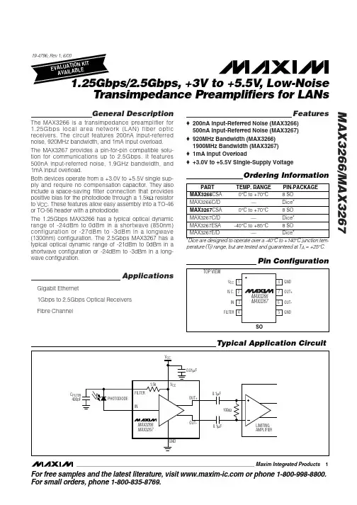
1.25Gbps/2.5Gbps, +3V to +5.5V, Low-Noise Transimpedance Preamplifiers for LANs
General Description
Features
o 200nA Input-Referred Noise (MAX3266) 500nA Input-Referred Noise (MAX3267) o 920MHz Bandwidth (MAX3266) 1900MHz Bandwidth (MAX3267) o 1mA Input Overload o +3.0V to +5.5V Single-Supply Voltage
VCC 0.01µF 1.5k CFILTER 400pF FILTER PHOTODIODE IN OUT+ VCC 0.1µF
100Ω OUT-
MAX3266 MAX3267
GND
0.1µF
LIMITING AMPLIFIER
________________________________________________________________ Maxim Integrated Products
Stresses beyond those listed under “Absolute Maximum Ratings” may cause permanent damage to the device. These are stress ratings only, and functional operation of the device at these or any other conditions beyond those indicated in the operational sections of the specifications is not implied. Exposure to absolute maximum rating conditions for extended periods may affect device reliability.
MAX3222E中文材料
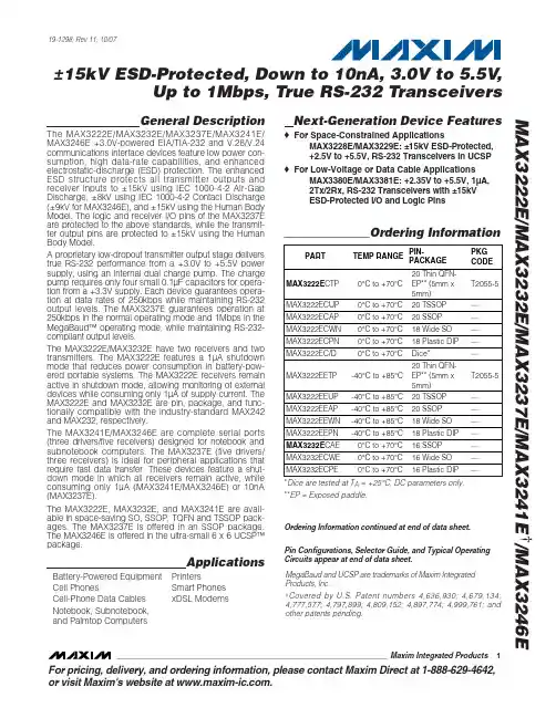
MAX3222E/MAX3232E/MAX3237E/MAX3241E/MAX3246E为+3.0V供电的EIA/TIA-232和V.28/V.24通信接口芯片,具有低功耗、高数据速率、增强型ESD保护等特性。
增强型ESD结构为所有发送器输出和接收器输入提供保护,可承受±15kV IEC 1000-4-2气隙放电、±8kV IEC 1000-4-2接触放电(MAX3246E为±9kV)和±15kV人体放电模式。
MAX3237E的逻辑引脚及接收器I/O引脚均提供上述保护,而它的发送器输出引脚提供±15kV人体放电模式的保护。
采用专有的低压差发送输出级,+3.0V至+5.5V供电时利用内部双电荷泵提供真正的RS-232性能。
工作于+3.3V电源时,荷泵仅需要四个0.1µF的小电容。
每款器件保证在250kbps数据速率下维持RS-232输出电平。
MAX3237E确保标准工作模式下提供250kbps的数据速率、在MegaBaud™工作模式下速率高达1Mbps。
MAX3222E/MAX3232E包括两个发送器和两个接收器;MAX3222E具有1µA关断模式,可降低电池供电便携式系统的功耗。
关断模式下,MAX3222E接收器仍保持有效状态,允许监视外设,而且仅消耗1µA的电源电流。
MAX3222E和MAX3232E的引脚、封装和功能分别兼容于工业标准的MAX242和MAX232。
MAX3241E/MAX3246E提供完备的串口(3个驱动器/5个接收器),专为笔记本电脑和亚笔记本电脑设计。
MAX3237E (5个驱动器/3个接收器)非常适合要求高速数据传输的外围设备。
这些器件都具有关断模式,此模式下所有接收器仍保持有效状态,而且仅消耗1µA (MAX3241E/MAX3246E)或10nA (MAX3237E)的电流。
MAX3222E、MAX3232E和MAX3241E都具有节省空间的SO、SSOP、TQFN及TSSOP封装,MAX3237E提供SSOP封装,MAX3246E提供超小型6 x 6 UCSP™封装。
DSC-CN3762
参数
符号
测试条件
输入电压范围
VCC
低电压锁存阈值
UVLO
芯片工作电流 恒压充电电压
电流检测
流入 BAT 管脚电流
涓流充电阈值 涓流充电阈值迟滞 充电结束阈值 再充电阈值 过压阈值
IVCC VREG
VCS
IBAT1 IBAT2 VPRE HPRE Iterm VRE Vov
VBAT>VREG 恒压充电,FB 连接到 BAT VBAT>VPRE,VCSP-VBAT VBAT<VPRE,VCSP-VBAT 充电结束模式,VBAT=7.4V 睡眠模式,VBAT=7.4V BAT管脚电压上升 BAT管脚电压下降 充电电流下降 BAT管脚电压下降 BAT 管脚电压上升
超出以上所列的极限参数可能造成器件的永久损坏。以上给出的仅仅是极限范围,在这样的极限条件下工作, 器件的技术指标将得不到保证,长期在这种条件下还会影响器件的可靠性。
3
Rev 1.0
如韵电子 CONSONANCE
电气特性:
(VCC=15V,TA=-40℃ 到 85℃,除非另有注明)
调整恒压充电电压
如果在CN3762的FB管脚和BAT管脚之间接一个电阻,可以提高恒压充电电压,以抵消电池内阻和连线电阻的 电压降,使得电池充电更饱满,如图3所示。
输入电压 9 VIN
FB 6
CN3762
Rx
GND BAT 7
如果采用图3中的连接方式,那么恒压充电电压典型值VREG为:
的正极。同时,此管脚和CSP管脚测量电流检测电阻RCS两端的
电压,并将此电压信号反馈给CN3762进行电流调制。 充电电流检测正输入端。此管脚和BAT管脚测量电流检测电阻
2N3763L中文资料
2N3763* 2N3765
60 60
Unit
Vdc Vdc Vdc Adc
TO-39* (TO-205AD) 2N3762, 2N3763
2N3762* 1 2N3763*
1.0
2N3764 2 2N3765
0.5 W
0
Total Power Dissipation @ TA = +250C Operating & Storage Junction Temp. Range
Output Capacitance VCB = 10 Vdc, IE = 0, 100 kHz ≤ f ≤ 1.0 MHz Input Capacitance VEB = 0.5 Vdc, IC = 0, 100 kHz ≤ f ≤ 1.0 MHz
SWITCHING CHARACTERISTICS
Street, Lawrence, MA 01841 1-800-446-1158 / (978) 794-1666 / Fax: (978) 689-0803
120101 Page 1 of 2
元器件交易网
2N3762, L, 2N3763, L, 2N3764, 2N3765 JAN SERIES
ELECTRICAL CHARACTERISTICS (con’t)
Characteristics Collector-Emitter Cutoff Current VEB = 2.0 Vdc, VCE = 20 Vdc VEB = 2.0 Vdc, VCE = 30 Vdc Emitter-Base Cutoff Current VEB = 2.0 Vdc VEB = 5.0 Vdc Symbol 2N3762, 2N3764 2N3763, 2N3765 All Types 2N3762, 2N3764 2N3763, 2N3765 ICEX Min. Max. 100 100 200 10 10 Unit ηAdc
MAX2682中文资料
元器件交易网
o <0.1µA Low-Power Shutdown Mode
o Ultra-Small Surface-Mount Packaging
Ordering Information
PART
TEMP. RANGE
PINPACKAGE
SOT TOP MARK
MAX2680EUT-T -40°C to +85°C 6 SOT23-6 AAAR
General Description
The MAX2680/MAX2681/MAX2682 miniature, low-cost, low-noise downconverter mixers are designed for lowvoltage operation and are ideal for use in portable communications equipment. Signals at the RF input port are mixed with signals at the local oscillator (LO) port using a double-balanced mixer. These downconverter mixers operate with RF input frequencies between 400MHz and 2500MHz, and downconvert to IF output frequencies between 10MHz and 500MHz.
MAX232中文资料.pdf
________________________________MAX220–MAX249 / Lj EIA/TIA-232E V.28/V.24 Lj ±12V ăӼ Lj 5μW ăMAX225ĂMAX233ĂMAX235 MAX245/MAX246/MAX247ԥ ԩ Lj ғ ă________________________________ӯRS-232 RS-232_______________________♦ Ă ESD үMAX3222E/MAX3232E/MAX3237E/MAX3241E/MAX3246E ǖ+3.0V +5.5V Ă Ă 1Mbps Ă 0.1μFRS-232 (MAX3246E UCSP TM )♦ ӊMAX221E ǖ±15kV ESD ү Ă+5V Ă1μA ĂAutoShutdown TM RS-232MAX220–MAX249+5V Ă RS-232/_____________________________________________________________________ ӹ19-4323; Rev 15; 1/06_____________________________ࢾ৪ቧᇦ)ኚ*Ᏼၫᓾ೯ࡼᔢઁ߲ă*ൡຢਖৃLj༿ᎧޣೊᇹăAutoShutdown UCSP Maxim Integrated Products, Inc. Ӷă۾ᆪဵNbyjnᑵါ፞ᆪᓾ೯ࡼፉᆪLjNbyjnݙ࣪डፉᒦࡀᏴࡼތፊᎅࠥޘညࡼࡇᇙঌᐊă༿ᓖፀፉᆪᒦభถࡀᏴᆪᔊᔝᒅडፉࡇᇙLjྙኊཀྵཱྀྀੜࠤᎫࡼᓰཀྵቶLj༿ݬఠNbyjnᄋࡼ፞ᆪۈᓾ೯ăჃནॅዹອਜ਼ᔢቤۈࡼၫᓾ೯Lj༿षᆰNbyjnࡼᓍǖxxx/nbyjn.jd/dpn/doăM A X 220–M A X 249+5V Ă RS-232 / 2_______________________________________________________________________________________ABSOLUTE MAXIMUM RATINGS—MAX220/222/232A/233A/242/243ELECTRICAL CHARACTERISTICS—MAX220/222/232A/233A/242/243(V CC = +5V ±10%, C1–C4 = 0.1μF‚ MAX220, C1 = 0.047μF, C2–C4 = 0.33μF, T A = T MIN to T MAX ‚ unless otherwise noted.)Note 1:For the MAX220, V+ and V- can have a maximum magnitude of 7V, but their absolute difference cannot exceed 13V.Note 2:Input voltage measured with T OUT in high-impedance state, SHDN or V CC = 0V.Note 3:Maximum reflow temperature for the MAX233A is +225°C.Stresses beyond those listed under “Absolute Maximum Ratings” may cause permanent damage to the device. These are stress ratings only, and functional operation of the device at these or any other conditions beyond those indicated in the operational sections of the specifications is not implied. Exposure to absolute maximum rating conditions for extended periods may affect device reliability.Supply Voltage (V CC )...............................................-0.3V to +6V V+ (Note 1)..................................................(V CC - 0.3V) to +14V V- (Note 1).............................................................+0.3V to +14V Input VoltagesT IN ..............................................................-0.3V to (V CC - 0.3V)R IN (Except MAX220)........................................................±30V R IN (MAX220).....................................................................±25V T OUT (Except MAX220) (Note 2).......................................±15V T OUT (MAX220)...............................................................±13.2V Output VoltagesT OUT ...................................................................................±15V R OUT .........................................................-0.3V to (V CC + 0.3V)Driver/Receiver Output Short Circuited to GND.........Continuous Continuous Power Dissipation (T A = +70°C)16-Pin Plastic DIP (derate 10.53mW/°C above +70°C).842mW18-Pin Plastic DIP (derate 11.11mW/°C above +70°C)..889mW 20-Pin Plastic DIP (derate 8.00mW/°C above +70°C)..440mW 16-Pin Narrow SO (derate 8.70mW/°C above +70°C)...696mW 16-Pin Wide SO (derate 9.52mW/°C above +70°C)......762mW 18-Pin Wide SO (derate 9.52mW/°C above +70°C)......762mW 20-Pin Wide SO (derate 10.00mW/°C above +70°C)....800mW 20-Pin SSOP (derate 8.00mW/°C above +70°C)..........640mW 16-Pin CERDIP (derate 10.00mW/°C above +70°C).....800mW 18-Pin CERDIP (derate 10.53mW/°C above +70°C).....842mW Operating Temperature RangesMAX2_ _AC_ _, MAX2_ _C_ _.............................0°C to +70°C MAX2_ _AE_ _, MAX2_ _E_ _..........................-40°C to +85°C MAX2_ _AM_ _, MAX2_ _M_ _.......................-55°C to +125°C Storage Temperature Range.............................-65°C to +160°C Lead Temperature (soldering, 10s) (Note 3)...................+300°CMAX220–MAX249+5V Ă RS-232/_______________________________________________________________________________________3OUT IN ELECTRICAL CHARACTERISTICS—MAX220/222/232A/233A/242/243 (continued)(V CC = +5V ±10%, C1–C4 = 0.1μF‚ MAX220, C1 = 0.047μF, C2–C4 = 0.33μF, T A = T MIN to T MAX ‚ unless otherwise noted.)M A X 220–M A X 249+5V Ă RS-232 / 4_______________________________________________________________________________________________________________________________________________________MAX220/MAX222/MAX232A/MAX233A/MAX242/MAX243108-1051525OUTPUT VOLTAGE vs. LOAD CURRENT-4-6-8-2642LOAD CURRENT (mA)O U T P U T V O L T A G E (V )1002011104104060AVAILABLE OUTPUT CURRENTvs. DATA RATE65798DATA RATE (kb/s)O U T P U T C U R R E N T (m A )203050+10V-10VMAX222/MAX242ON-TIME EXITING SHUTDOWN+5V +5V 0V0V 500μs/div V +, V - V O L T A G E (V )ELECTRICAL CHARACTERISTICS—MAX220/222/232A/233A/242/243 (continued)(V CC = +5V ±10%, C1–C4 = 0.1μF‚ MAX220, C1 = 0.047μF, C2–C4 = 0.33μF, T A = T MIN to T MAX ‚ unless otherwise noted.)MAX220–MAX249+5V Ă RS-232/_______________________________________________________________________________________5V CC ...........................................................................-0.3V to +6V V+................................................................(V CC - 0.3V) to +14V V-............................................................................+0.3V to -14V Input VoltagesT IN ............................................................-0.3V to (V CC + 0.3V)R IN ......................................................................................±30V Output VoltagesT OUT ...................................................(V+ + 0.3V) to (V- - 0.3V)R OUT .........................................................-0.3V to (V CC + 0.3V)Short-Circuit Duration, T OUT ......................................Continuous Continuous Power Dissipation (T A = +70°C)14-Pin Plastic DIP (derate 10.00mW/°C above +70°C)....800mW 16-Pin Plastic DIP (derate 10.53mW/°C above +70°C)....842mW 20-Pin Plastic DIP (derate 11.11mW/°C above +70°C)....889mW 24-Pin Narrow Plastic DIP(derate 13.33mW/°C above +70°C)..........1.07W24-Pin Plastic DIP (derate 9.09mW/°C above +70°C)......500mW 16-Pin Wide SO (derate 9.52mW/°C above +70°C).........762mW20-Pin Wide SO (derate 10.00mW/°C above +70°C).......800mW 24-Pin Wide SO (derate 11.76mW/°C above +70°C).......941mW 28-Pin Wide SO (derate 12.50mW/°C above +70°C) .............1W 44-Pin Plastic FP (derate 11.11mW/°C above +70°C).....889mW 14-Pin CERDIP (derate 9.09mW/°C above +70°C)..........727mW 16-Pin CERDIP (derate 10.00mW/°C above +70°C)........800mW 20-Pin CERDIP (derate 11.11mW/°C above +70°C)........889mW 24-Pin Narrow CERDIP(derate 12.50mW/°C above +70°C)..............1W24-Pin Sidebraze (derate 20.0mW/°C above +70°C)..........1.6W 28-Pin SSOP (derate 9.52mW/°C above +70°C).............762mW Operating Temperature RangesMAX2 _ _ C _ _......................................................0°C to +70°C MAX2 _ _ E _ _...................................................-40°C to +85°C MAX2 _ _ M _ _................................................-55°C to +125°C Storage Temperature Range.............................-65°C to +160°C Lead Temperature (soldering, 10s) (Note 4)...................+300°CABSOLUTE MAXIMUM RATINGS—MAX223/MAX230–MAX241ELECTRICAL CHARACTERISTICS—MAX223/MAX230–MAX241(MAX223/230/232/234/236/237/238/240/241, V CC = +5V ±10%; MAX233/MAX235, V CC = 5V ±5%‚ C1–C4 = 1.0μF; MAX231/MAX239,V CC = 5V ±10%; V+ = 7.5V to 13.2V; T A = T MIN to T MAX ; unless otherwise noted.)Stresses beyond those listed under “Absolute Maximum Ratings” may cause permanent damage to the device. These are stress ratings only, and functional operation of the device at these or any other conditions beyond those indicated in the operational sections of the specifications is not implied. Exposure to absolute maximum rating conditions for extended periods may affect device reliability.Note 4:Maximum reflow temperature for the MAX233/MAX235 is +225°C.M A X 220–M A X 249+5V Ă RS-232 / 6_______________________________________________________________________________________ELECTRICAL CHARACTERISTICS—MAX223/MAX230–MAX241 (continued)(MAX223/230/232/234/236/237/238/240/241, V CC = +5V ±10%; MAX233/MAX235, V CC = 5V ±5%‚ C1–C4 = 1.0μF; MAX231/MAX239,V CC = 5V ±10%; V+ = 7.5V to 13.2V; T A = T MIN to T MAX ; unless otherwise noted.)MAX220–MAX249+5V Ă RS-232/_______________________________________________________________________________________7_______________________________________________________________MAX223/MAX230–MAX2418.56.54.55.5TRANSMITTER OUTPUT VOLTAGE (V OH ) vs. V CC7.08.0V CC (V)V O H (V )5.07.57.46.02500TRANSMITTER OUTPUT VOLTAGE (V OH )vs. LOAD CAPACITANCE AT DIFFERENT DATA RATES6.46.27.27.0LOAD CAPACITANCE (pF)V O H (V )1500100050020006.86.612.04.02500TRANSMITTER SLEW RATE vs. LOAD CAPACITANCE6.05.011.09.010.0LOAD CAPACITANCE (pF)S L E W R A T E (V /μs )1500100050020008.07.0-6.0-9.04.55.5TRANSMITTER OUTPUT VOLTAGE (V OL ) vs. V CC-8.0-8.5-6.5-7.0V CC (V)V O L (V )5.0-7.5-6.0-7.62500TRANSMITTER OUTPUT VOLTAGE (V OL )vs. LOAD CAPACITANCE AT DIFFERENT DATA RATES-7.0-7.2-7.4-6.2-6.4LOAD CAPACITANCE (pF)V O L (V )150010005002000-6.6-6.810-105101520253035404550TRANSMITTER OUTPUT VOLTAGE (V+, V-)vs. LOAD CURRENT-2-6-4-886CURRENT (mA)V +, V - (V )420*SHUTDOWN POLARITY IS REVERSED FOR NON MAX241 PARTSV+, V- WHEN EXITING SHUTDOWN(1μF CAPACITORS)MAX220-13SHDN*V-O V+500ms/divM A X 220–M A X 249+5V Ă RS-232 / 8_______________________________________________________________________________________ABSOLUTE MAXIMUM RATINGS—MAX225/MAX244–MAX249ELECTRICAL CHARACTERISTICS—MAX225/MAX244–MAX249(MAX225, V CC = 5.0V ±5%; MAX244–MAX249, V CC = +5.0V ±10%, external capacitors C1–C4 = 1μF; T A = T MIN to T MAX ; unless oth-erwise noted.)Stresses beyond those listed under “Absolute Maximum Ratings” may cause permanent damage to the device. These are stress ratings only, and functional operation of the device at these or any other conditions beyond those indicated in the operational sections of the specifications is not implied. Exposure to absolute maximum rating conditions for extended periods may affect device reliability.Supply Voltage (V CC )...............................................-0.3V to +6V Input VoltagesT IN ‚ ENA , ENB , ENR , ENT , ENRA ,ENRB , ENTA , ENTB ..................................-0.3V to (V CC + 0.3V)R IN .....................................................................................±25V T OUT (Note 5).....................................................................±15V R OUT ........................................................-0.3V to (V CC + 0.3V)Short Circuit (one output at a time)T OUT to GND............................................................Continuous R OUT to GND............................................................ContinuousContinuous Power Dissipation (T A = +70°C)28-Pin Wide SO (derate 12.50mW/°C above +70°C).............1W 40-Pin Plastic DIP (derate 11.11mW/°C above +70°C)...611mW 44-Pin PLCC (derate 13.33mW/°C above +70°C)...........1.07W Operating Temperature RangesMAX225C_ _, MAX24_C_ _ ..................................0°C to +70°C MAX225E_ _, MAX24_E_ _ ...............................-40°C to +85°C Storage Temperature Range.............................-65°C to +160°C Lead Temperature (soldering,10s) (Note 6)....................+300°CNote 5:Input voltage measured with transmitter output in a high-impedance state, shutdown, or V CC = 0V.Note 6:Maximum reflow temperature for the MAX225/MAX245/MAX246/MAX247 is +225°C.MAX220–MAX249+5V Ă RS-232/_______________________________________________________________________________________9Note 7:The 300Ωminimum specification complies with EIA/TIA-232E, but the actual resistance when in shutdown mode or V CC =0V is 10M Ωas is implied by the leakage specification.ELECTRICAL CHARACTERISTICS—MAX225/MAX244–MAX249 (continued)(MAX225, V CC = 5.0V ±5%; MAX244–MAX249, V CC = +5.0V ±10%, external capacitors C1–C4 = 1μF; T A = T MIN to T MAX ; unless oth-erwise noted.)M A X 220–M A X 249+5V Ă RS-232 / 10_____________________________________________________________________________________________________________________________________________________MAX225/MAX244–MAX24918212345TRANSMITTER SLEW RATE vs. LOAD CAPACITANCE86416LOAD CAPACITANCE (nF)T R A N S M I T T E R S L E W R A T E (V /μs )14121010-105101520253035OUTPUT VOLTAGEvs. LOAD CURRENT FOR V+ AND V--2-4-6-88LOAD CURRENT (mA)O U T P U T V O L T A G E (V )64209.05.012345TRANSMITTER OUTPUT VOLTAGE (V+, V-)vs. LOAD CAPACITANCE AT DIFFERENT DATA RATES6.05.58.5LOAD CAPACITANCE (nF)V +, V (V )8.07.57.06.5MAX220–MAX249+5V RS-232/1. 2.3. 4.M A X 220–M A X 249+5V RS-232 / ENT ENR OPERATION STATUS TRANSMITTERSRECEIVERS00Normal Operation All Active All Active 01Normal Operation All Active All 3-State10Shutdown All 3-State All Low-Power Receive Mode 11ShutdownAll 3-StateAll 3-Stateӹ1a. MAX245ENT ENR OPERATION STATUS TRANSMITTERS RECEIVERSTA1–TA4TB1–TB4RA1–RA5RB1–RB500Normal Operation All Active All Active All Active All Active 01Normal Operation All Active All Active RA1–RA4 3-State,RA5 Active RB1–RB4 3-State,RB5 Active 1ShutdownAll 3-StateAll 3-StateAll Low-Power Receive Mode All Low-Power Receive Mode 11Shutdown All 3-State All 3-StateRA1–RA4 3-State,RA5 Low-Power Receive ModeRB1–RB4 3-State,RB5 Low-Power Receive Modeӹ1b. MAX245ӹ1c. MAX246ENA ENB OPERATION STATUS TRANSMITTERS RECEIVERSTA1–TA4TB1–TB4RA1–RA5RB1–RB500Normal Operation All Active All Active All Active All Active 01Normal Operation All Active All 3-State All Active RB1–RB4 3-State,RB5 Active 1ShutdownAll 3-StateAll ActiveRA1–RA4 3-State,RA5 Active All Active 11Shutdown All 3-State All 3-StateRA1–RA4 3-State,RA5 Low-Power Receive ModeRB1–RB4 3-State,RA5 Low-Power Receive ModeMAX220–MAX249+5V RS-232/M A X 220–M A X 249____________________________MAX220–MAX249Ҫ 4 ԩ ǖ ӏDC-DC ĂRS-232 ĂRS-232 Lj ăӏMAX220–MAX249 ԩ ӏLj +5V ±10V ( )Lj RS-232 ă C1 +5V ӂLj V+ C3 +10V Ǘ C2 +10V V- C4 -10V ă+10V (V+) -10V (V-) Lj ԩ (Ը ԩ )Ǘ MAX225 MAX245–MAX247 Lj ԥ ăV+ V- Lj ă V+ĂV- ԩ Lj ԥ V+ĂV- EIA/TIA-232E ±5V ăMAX222ĂMAX225ĂMAX230ĂMAX235ĂMAX236ĂMAX240ĂMAX241 MAX245–MAX249 Lj Ө V+ V- ԩ ă LjV- 0V LjV+ +5V ă +10V ԩ V+ ( ԥ ԩ ӏ դ +10V) Lj ԥ Ѡ C1LjԌ Ӥ SHDN V CC Lj V+Ӈ ԩ V CC ăRS-232Ӷ 5kΩ RS-232 LjԌ V CC =+5V Lj ҈ ±8V ă ҈ ү EIA/TIA-232E V.28 Lj ±5V Lj Ҫ 3kΩ ĂV CC = +4.5V ă (V +-1.3V) (V- +0.5V)ăTTL CMOS ă ԥ Lj Ă V CC 400kΩ (MAX220 )ă Lj ă Ӈ Lj ԩ ի 12μA ă Ă ӇLj ӡLjԌ Lj ի Ѡ( 25μA)ă Ӈ ±15V ă Lj ի 8μA ăMAX220ԥ ӄ ԩ Lj ԥ Lj GND V CC ăMAX239 Lj MAX223ĂMAX225ĂMAX235ĂMAX236ĂMAX240 MAX241 ӄ ăӹ2 ă( MAX225/MAX235/MAX236/MAX239–MAX241)Lj TTL/CMOS Ă Ǘ Lj Lj ăLj Ӈ ӡLj 1μA Lj Ӈ ă 1μA Lj ӯ Ӈ 0V (V CC +6V)ă -0.5V Lj Lj 1kΩ ă Ӈ V CC +6V Lj 1kΩ ă҈ 30V/μs Lj EIA/TIA-232E V.28 ă҈ ǖ 24V/μs Lj3Ω 2500pF 10V/μs ăRS-232EIA/TIA-232E V.28 3V 0Lj Lj ă 0.8V 2.4V Lj TTL Lj EIA/TIA-232E V.28 ă±25V LjԌ Ӷ 5kΩ ă V.28 EIA/TIA-232E ă+5V RS-232 /ӹMAX220–MAX249+5V RS-232/0.5V LjԌ ү0.2V ă Lj Ӱ դ ӰLj ă 600ns Lj ҈ ăMAX223ĂMAX242 MAX245–MAX249 Lj IC Lj ă ի ă Lj Lj ӄ Ă ă Ճ ă—MAX243MAX243 MAX232A Lj Ӽ RS-232 ү ă CTS RTS Ӈ Lj ԥ ăԥӤ ԥ ԥ ӄăү -0.8V Lj ԥ +1.4V ă Lj ԯӰ ă Lj 0Lj Đ đ ă իLjMAX243 (+1.4V ) (TD RD)Lj (DTR ĂDTS ĂCTS ĂRTS ) ăRS-232 դ Ѣ EIA/TIA-232E LjԳ ү ă Ӈ Ă Lj Ӱ ă IC ă Ө Lj Ӥ Ӈ Lj ă—MAX222–MAX242LjMAX222ĂMAX235ĂMAX236ĂMAX240 MAX241 Ӈ ă LjMAX223 MAX242 ү ă Lj ӰLj 2.5μs ă Lj CMOS ăMAX223 MAX242 ( MAX242 EN ĂMAX223 EN)Lj SHDN ( MAX241 SHDN) ă SHDN ( MAX241 SHDN ) ăMAX225 5 5 ǗMAX245 10 8 ă ă ENT Lj ӏ ӡԌ ă Lj 25μA Lj ү Lj ( )ăMAX225 5 ENR ăMAX245 8 ENR Lj (RA5 RB5) ү ă ENR LjRA1–RA4 RB1–RB4 ăMAX225 MAX245–MAX249 ăǖ ( ի )Ă ( ) ( ү )ă ă ǖ ( ի ) ( )ă Ӈ ă Ӈ Lj ă Lj ăM A X 220–M A X 249ӹ1a–1d ăMAX244 Lj Ҫ ӹ ăMAX246 10 8 Lj Lj Ӽ ՊăA Պ (ENA ) Lj 4 A Պ Ǘ LjB Պ (ENB ) 4 B Պ ă MAX245 Lj A Պ B Պ (RA5 RB5) ү ă A ՊĂB Պ Ӈ (ENA =ENB =+5V) Lj ăMAX247 9 8 Lj 4 ăENRA ĂENRB Lj Ӽ 4 ăENTA ĂENTB Lj Ӽ 4 ă 9 (RB5) ă ENTA ENTB ăMAX248 8 8 Lj 4 ăENRA ĂENRB Lj Ӽ 4ăENTA ĂENTB Lj Ӽ 4 ă ă ENTA ĂENTB Lj ăMAX249 10 6 Lj 4 ăENRA ĂENRB Lj Ӽ 5 ăENTA ĂENTB Lj Ӽ 3 ă ă ENTA ĂENTB Lj ă Ljү Lj 20kb/s ă____________________________5 25 ă LjV CC C1ĂC2 Lj ҈ ă+5V RS-232 /MAX220–MAX249+5V RS-232/5. MAX220/MAX232/MAX232A6. MAX222/MAX242M A X 220–M A X 249+5V RS-232 /7. MAX225MAX220–MAX249+5V RS-232/8. MAX223/MAX241M A X 220–M A X 249+5V RS-232 /9. MAX23010. MAX231MAX220–MAX249+5V RS-232/12. MAX23411. MAX233/MAX233AM A X 220–M A X 249+5V RS-232 /13. MAX235MAX220–MAX249+5V RS-232/14. MAX236M A X 220–M A X 249+5V RS-232 /15. MAX237MAX220–MAX249+5V RS-232/16. MAX238M A X 220–M A X 249+5V RS-232 /17. MAX239MAX220–MAX249+5V RS-232/18. MAX240M A X 220–M A X 249+5V RS-232 /19. MAX243MAX220–MAX249+5V RS-232/20. MAX244M A X 220–M A X 249+5V RS-232 /21. MAX245MAX220–MAX249+5V RS-232/______________________________________________________________________________________3122. MAX246M A X 220–M A X 249+5V RS-232 / 32______________________________________________________________________________________23. MAX247MAX220–MAX249+5V RS-232/______________________________________________________________________________________3324. MAX248M A X 220–M A X 249+5V RS-232 / 34______________________________________________________________________________________25. MAX249MAX220–MAX249+5V RS-232/______________________________________________________________________________________35_____________________________________________________________________ ( )*ൡຢਖৃLj༿ᎧޣೊᇹăM A X 220–M A X 249+5V RS-232 / _____________________________________________________________________ ( )*ൡຢਖৃLj༿Ꭷޣೊᇹă____________________________Lj Փ /packages ă_____________________________Rev 15 ǖ2–5Ă8Ă9Ă36ăNbyjnݙ࣪Nbyjnޘອጲᅪࡼྀੜ࢟വဧঌᐊLjጐݙᄋᓜಽభăNbyjnۣഔᏴྀੜဟମĂᎌྀੜᄰۨࡼ༄ᄋሆኀখޘອᓾ೯ਜ਼ਖৃࡼཚಽă36____________________Maxim Integrated Products, 120 San Gabriel Drive, Sunnyvale, CA 94086 408-737-7600©2006 Maxim Integrated ProductsNbyjn ဵNbyjn!Joufhsbufe!Qspevdut-!Jod/ࡼᓖݿܪăNbyjn ۱யێူࠀ۱ய9439ቧረᎆᑶܠ൩211194ॅ࢟જǖ911!921!1421࢟જǖ121.732262::ࠅᑞǖ121.732263::。
Woodward SPM-D2-10系列产品规范37622B 2 3相AC生成机同步器说明书
SPM-D2-10 SeriesProduct Specification37622BSynchronizersfor 2/3-phase AC Gen-Sets∙Synchronization for one or two circuit breakers ∙Frequency, Phase and Voltage Matching ∙Selectable control out-puts for speed and volt-age biasing∙Compatible with a wide range of GOVs and AVRs∙Circuit breaker time compensation ∙Two lines bright LCD display for generator and bus values ∙Front face synchrono-scope for easy commis-sioning∙True RMS measurement for reliable operation∙Configurable through HMI or PC∙Wide range power sup-ply available ∙Switchable parameter sets available ∙CE Marked (RoHS 2compliant)∙UL/cUL ListedDESCRIPTIONWoodward understands the time-intensive nature of Power Generation projects. Ensuring the lon-gevity of components is one way we can make our customers successful. Woodward has supplied and supported the well-established SPM-D line of synchronizers for 20+ years. With the state of the art Drop-In replacement successor, SPM-D2 the life of this synchronizer line is now extended. All of the SPM-D2 synchronizers are password protected and are configurable either through HMI as before or through ToolKit configuration tool with USB connectivity.The SPM-D2-10 series are microprocessor-based synchronizers designed for use on two or three phase AC generators equipped with Woodward or other compatible speed controls and automatic voltage regulators. The SPM-D2-10 synchronizers provide automatic frequency, phase and voltage matching using either analog- or discrete output bias signals. These synchronizers are applied to a wide range of prime movers and generators, as its control signals may be set to fit several types of gensets - from fast reacting diesel engines to soft reacting gas turbines.The SPM-D2-10 synchronizers are available in 3 base models:∙SPM-D2-10 … : provides 1-phase / 2-wire voltage measurement with options for analog and/or discrete biasing signals and wide range power supply ∙SPM-D2-10 …/YB : provides 3-phase / 4-wire voltage measurement with discrete biasing signals and option for wide range power supply ∙SPM-D2-10 …/PSY5: provides 1-phase / 2-wire voltage measurement with discrete biasing sig-nals, option for wide range power supply and 2 sets of switchable parameter set.FEATURES∙Phase match or slip frequency synchronization with voltage matching∙Two-Phase or three-phase true RMS voltage sensing of generator and bus with Class I accuracy ∙Selectable operating modes like SPM-A (Run, Check, Permissive and Off)∙Synch-Check and synchronization time monitoring ∙Dead bus closing of CB on demand∙ 2 setting blocks, each containing 7 configurable parameters (in PSY5 variants) selectable through DI: Frequency/Voltage control dead-band, Frequency/Voltage control time pulse, Fre-quency/Voltage control gain, Circuit breaker time compensation∙Control outputs: Discrete raise/lower for speed and voltage in all variants, | X and XN variants:also configurable analog signals (Voltage, Current and PWM)∙Voltage and frequency control in isolated operation∙Two line bright liquid crystal display for operation, alarm, measuring values visualization and parametrization∙Front face with synchronoscope and indication of breaker state/control activity ∙Multi-level password protection of parameters∙Woodward ToolKit™ software for configuration via USB ∙Two built-in languages: English, GermanNew Features✓USB connectivity to PC✓ToolKit configuration support✓Password protection to all variants ✓Same look & feel as SPM-D ✓Drop-In replacementSPECIFICATIONSPower supply[Standard] ..........................................................12/24 V DC (9.5 to 32 V DC) [N, XN and NYB Packages] .................... 90 to 250Vac / 120 to 375 Vdc; ............................................ 100 to 240 Vac -15%/+10% (UL rating only) Intrinsic consumption ................................................................. max. 10 W Ambient temperature (operation) ............................................. -20 to 70 °C[N, XN and NYB Packages] -20 to 60 °C Ambient temperature (storage) ................................................ -30 to 80 °C Ambient humidity....................................................... 95%, non-condensing Voltage .............................................................................................. ( / )[1] 100 Vac Rated (V rated) ............................................ 66/115 V ACMax. value (V max) ................................................. 150 V AC or [4] 400 Vac Rated (V rated) .......................................... 230/400 V AC Max. value (V max) ................................................. 300 V AC Rated surge volt. (V surge) .............................. [1] 2.5kV, [4] 4.0 kV Accuracy .......................................................................................... C lass 1 Measuring frequency............................................... 50/60 Hz (40 to 70 Hz) Linear measuring range ........................................................... 1.3 x Vrated Input resistance ...................................... [1]0.21 MOhms, [4]0.696 MOhms Current Rated (I rated) .................................................. [1].../1A,[5] (5)Linear measuring range ................................................................. 3.0×I rated Burden .......................................................................................... < 0.15 VA Rated short-time overcurrent (1 s) ..........................[1] 50×I rated, [5] 10×I rated Discrete inputs .............................................................................. i solated Input range ...................................................12/24 V DC or 18 to 250 Vac/dc Input resistance ........................................ a pprox. 6.8 kOhms or 68 kOhms Relay outputs .................................................................................... isolated Contact material ................................................................................... A gCdO Load (GP) (V cont, relay output) AC:.......................................... 2.00 A AC@250 V AC DC: 2.00 A DC@24 V DC / 0.36 A DC@125 V DC / 0.18 A DC@250 V DC Pilot Duty (PD) AC: ................................................................................. B300 DC: 1.00 A DC@24 V DC / 0.22 A DC@125 V DC / 0.10 A DC@250 V DC Analog Outputs (isolated)......................................................freely scalable Type ......................................................................... ± 10 V / ± 20 mA / PWM Insulation voltage (continuously, AVR out) ......................................... 300 V AC Insulation voltage (continuously, Gov out) .......................................... 100 V AC Resolution .............................................................................................. 12 Bit ± 10 V (scalable) .............................................. i nternal resistance 500 Ohms ± 20 mA (scalable) ................................................ maximum load 500 Ohms Housing Front panel flush mounting ............. Type APRANORM DIN 43 700 Dimensions WxHxD .......................................... 144 × 72 × 122 mm Front cutout WxH .................................... 138 [+1.0] × 68 [+0.7] mm Connection (screw/plug terminals depending on connector) .. 1.5 mm² or 2.5 mm² Front .................................................................................... insulating surface Protection System / Sealing .............................................................................Front ................................. I P42 with correct installationFront ....................... IP54 (with gasket P/N 8923-1037)Back ...................................................................... IP20 Weight ........................................................................................approx. 800 g Listings tested according to applicable IEC standards .................................. ......................................................... C E, UL/cUL listing for ordinary locationsMarine (Pending)........................ LR (Type Approval), ABS (Type Approval) DIMENSIONSTERMINAL DIAGRAMNOTE The terminals used for connection depend on the implemented functionality of each package.The drawing below gives an overview with sample package XN– for details please see the dedicated Technical Manual listed in the features table at the rear page.RELATED PRODUCTS∙Load Share Synchronizer SPM-D2-11 (Product Specification # 37623)∙Digital Synchronizer and Load Control DSLC-2 (Product Specification # 37493)∙Master Synchronizer and Load Control MSLC-2 (Product Specification # 37494)∙Load Share speed control 2301E (Product Specification # 03404)∙Load Sharing Module LSM (Product Specification # 82686)∙SPM-A Synchronizer (Product Specification # 82383)∙Power Generation Learning Module (Product Specification # 03412): P/N 8447-1012CONTACTSubject to technical modifications. This document is distributed for informa-tional purposes only. It is not to be con-strued as creating or becoming part of any Woodward Company contractual or warranty obligation unless expressly stated in a written sales contract.We appreciate your comments about the content of our publications. Please send comments including the document num-ber below to*********************© WoodwardAll Rights Reserved 37622B - 2017/01/Stuttgart FEATURES OVERVIEW#1 Dead bus start functionalityOn-Demand: Closing of CB on demandEnhanced: Black start (closing to de-energized second side of a breaker for followingconditions):- dead system 1 - live system 2- live system 1 - dead system 2- dead system 1 - dead system 2#2 Switch from Parameter set #A to #B by activating DI #6#3 Configurable to either speed or voltage#4 Analog bias outputs for voltage and speed freely configurable for all levels (+/-1 V, +/-3 V,0 to 5 V, 0.5 to 4.5 V, +/-10 V +/-5 V, 0 to 20 mA, +/-20 mA, and much more)#5 Speed bias output configurable as 500 Hz PWM output with adjustable voltage level#6 All units with 400 V measuring inputs can also be used for 100 V system voltage AvKgenerátoryul.4.kvetna75501 Vsetintel:+420 571 413322fax+420 571 413322email:info@woodward-seg.czwww.woodward-seg.cz。
- 1、下载文档前请自行甄别文档内容的完整性,平台不提供额外的编辑、内容补充、找答案等附加服务。
- 2、"仅部分预览"的文档,不可在线预览部分如存在完整性等问题,可反馈申请退款(可完整预览的文档不适用该条件!)。
- 3、如文档侵犯您的权益,请联系客服反馈,我们会尽快为您处理(人工客服工作时间:9:00-18:30)。
Note 1: Dice are tested at TA = +25°C. Note 2: Outputs terminated with 50Ω to VCC - 2V. Note 3: Voltage measurements are relative to VCC.
2
_______________________________________________________________________________________
________________________Applications
622Mbps LAN/ATM LAN Receivers 155Mbps LAN/ATM LAN Receivers
*Dice are designed to operate from -40°C to +85°C, but are tested and guaranteed only at TA = +25°C. +Denotes a lead-free/RoHS-compliant package.
DC ELECTRICAL CHARACTERISTICS
(VCC = +4.5V to +5.5V, DISABLE = low, TA = -40°C to +85°C, unless otherwise noted. Typical values are at VCC = +5.0V, TA = +25°C.) (Note 1) PARAMETER Power-Supply Current LOS Output TTL High LOS Output TTL Low LOS Output PECL High LOS Output PECL Low DISABLE Input Current DISABLE Input High DISABLE Input Low DISABLE Input PECL High DISABLE Input PECL Low PECL Data Output Voltage High (VOH) PECL Data Output Voltage Low (VOL) Disabled Differential Output Disabled Common-Mode Output MAX3761, IVCC MAX3762, IVCC MAX3761 MAX3761 (TA = +25°C to +85°C) (TA = -40°C to +25°C) -1150 -1830 2.65 0.8 -1160 -1470 -1150 -1830 -100 VCC - 0.7 -880 -1555 100 VCC -1.2 2.8 0.40 0.44 -880 -1555 100 CONDITIONS MIN TYP 25 30 MAX 37 46 UNITS mA V V mV mV μA V V mV mV mV mV mV V
_______________General Description
The MAX3761/MAX3762 limiting amplifiers, with 4mV sensitivity and PECL data outputs, are optimized for operation in low-cost, 622Mbps, LAN/ATM LAN fiber optics applications. An integrated power detector senses the input signal’s amplitude. A received-signal-strength indicator (RSSI) gives an analog indication of the power level, while the complementary loss-of-signal (LOS) outputs indicate if the input power level exceeds the programmed threshold level. The LOS threshold can be adjusted to detect signal amplitudes between 3mVp-p and 100mVp-p, providing a 15dB LOS adjustment in fiber optic receivers. The LOS outputs have 3.5dB of hysteresis, which prevents chatter when input signal levels are small. The MAX3761’s LOS outputs are compatible with TTL-logic levels. The MAX3762 has PECL LOS outputs. DISABLE and LOS can be used to implement a squelch function, which turns off the data outputs when the input signal is below the programmed threshold.
+5V 10nF RSSI VCCO 100pF BYPASS SUPPLY CIN 5.6nF VIN+ CIN 5.6nF VINVCC EN CZP CZN DISABLE LOS+ LOSOUTOUT+ 50Ω 50Ω GNDO GND VTH SUB VCC - 2V CAZ 150pF
MAX3761 MAX3762
Stresses beyond those listed under “Absolute Maximum Ratings” may cause permanent damage to the device. These are stress ratings only, and functional operation of the device at these or any other conditions beyond those indicated in the operational sections of the specifications is not implied. Exposure to absolute maximum rating conditions for extended periods may affect device reliability.
16 VCCO 15 OUT+ 14 OUT13 GNDO 12 VTH 11 INV
MAX3761
ห้องสมุดไป่ตู้
FILTER 100pF +VCC R1 100kΩ R2 22kΩ CFILTER INV
QSOP
MAX3762 at end of data sheet.
________________________________________________________________ Maxim Integrated Products 1
元器件交易网
Low-Power, 622Mbps Limiting Amplifiers with Chatter-Free Power Detect for LANs
♦ Chatter-Free Power Detector with Programmable Loss-of-Signal Outputs ♦ 4mV Input Sensitivity ♦ PECL Data Outputs ♦ Single 5V Power Supply ♦ 250ps Output Edge Speed ♦ Low 15ps Pulse-Width Distortion ♦ TTL Loss-of-Signal Interface Logic—MAX3761 ♦ PECL Loss-of-Signal Interface Logic—MAX3762
MAX3761/MAX3762
Ordering Information
PART MAX3761EEP+ MAX3761E/D MAX3762EEP+ MAX3762E/D TEMP RANGE -40°C to +85°C -40°C to +85°C -40°C to +85°C -40°C to +85°C PIN-PACKAGE 20 QSOP Dice* 20 QSOP Dice*
元器件交易网
19-1097; Rev 4; 8/08
KIT ATION EVALU LE B A IL A AV
Low-Power, 622Mbps Limiting Amplifiers with Chatter-Free Power Detect for LANs
____________________________Features
Low-Power, 622Mbps Limiting Amplifiers with Chatter-Free Power Detect for LANs
MAX3761/MAX3762
ABSOLUTE MAXIMUM RATINGS
VCC, VCCO............................................................-0.5V to +7.0V FILTER, RSSI, EN, VIN+, VIN-, CZP, CZN, DISABLE, LOS+, LOS-, INV, VTH...............-0.5V to (VCC + 0.5V) PECL Output Current (OUT+, OUT-, LOS+, LOS-) ............50mA Continuous Power Dissipation (TA = +85°C) QSOP (derate 9.1mW/°C above +85°C) .......................591mW Operating Junction Temperature Range ...........-40°C to +150°C Processing Temperature (die) .........................................+400°C Storage Temperature Range .............................-65°C to +160°C Lead Temperature (soldering, 10sec) .............................+300°C