MAX5419PETA+T中文资料
MAXIM MAX500 说明书

现货库存、技术资料、百科信息、热点资讯,精彩尽在鼎好!For free samples & the latest literature: , or phone 1-800-998-8800_______________General DescriptionThe MAX500 is a quad, 8-bit, voltage-output digital-to-analog converter (DAC) with a cascadable serial inter-face. The IC includes four output buffer amplifiers and input logic for an easy-to-use, two- or three-wire serial interface. In a system with several MAX500s, only one serial data line is required to load all the DACs by cas-cading them. The MAX500 contains double-buffered logic and a 10-bit shift register that allows all four DACs to be updated simultaneously using one control signal.There are three reference inputs so the range of two of the DACs can be independently set while the other two DACs track each other.The MAX500 achieves 8-bit performance over the full operating temperature range without external trimming.________________________ApplicationsMinimum Component Count Analog Systems Digital Offset/Gain Adjustment Industrial Process Control Arbitrary Function Generators Automatic Test Equipment____________________________Featureso Buffered Voltage Outputs o Double-Buffered Digital Inputso Microprocessor and TTL/CMOS Compatible o Requires No External Adjustmentso Two- or Three-Wire Cascadable Serial Interface o 16-Pin DIP/SO Package and 20-Pin LCC o Operates from Single or Dual Supplies______________Ordering InformationMAX500CMOS, Quad, Serial-Interface8-Bit DAC________________________________________________________________Maxim Integrated Products1_________________Pin Configurations________________Functional Diagram19-1016; Rev 2; 2/96*Contact factory for dice specifications.M A X 500CMOS, Quad, Serial-Interface 8-Bit DAC 2_______________________________________________________________________________________ABSOLUTE MAXIMUM RATINGSELECTRICAL CHARACTERISTICS—Dual Supplies(V= +11.4V to +16.5V, V = -5V ±10%, AGND = DGND = 0V, V = +2V to (V - 4V), T = T to T , unless otherwise noted.)Stresses beyond those listed under “Absolute Maximum Ratings” may cause permanent damage to the device. These are stress ratings only, and functional operation of the device at these or any other conditions beyond those indicated in the operational sections of the specifications is not implied. Exposure to absolute maximum rating conditions for extended periods may affect device reliability.Power RequirementsV DD to AGND...........................................................-0.3V, +17V V DD to DGND..........................................................-0.3V, +17V V SS to DGND..................................................-7V, (V DD + 0.3V)V DD to V SS ...............................................................-0.3V, +24V Digital Input Voltage to DGND....................-0.3V, (V DD + 0.3V)V REF to AGND.............................................-0.3V, (V DD + 0.3V)V OUT to AGND (Note 1)...............................-0.3V, (V DD + 0.3V)Power Dissipation (T A = +70°C)Plastic DIP (derate 10.53mW/°C above +70°C)............842mWWide SO (derate 9.52mW/°C above +70°C)................762mW CERDIP (derate 10.00mW/°C above +70°C)...............800mW LCC (derate 9.09mW/°C above +70°C).......................727mW Operating Temperature RangesMAX500_C_ _....................................................0°C to + 70°C MAX500_E_ _...................................................-40°C to +85°C MAX500_M_ _................................................-55°C to +125°C Storage Temperature Range.............................-65°C to +150°C Lead Temperature (soldering, 10sec).............................+300°CNote 1:The outputs may be shorted to AGND, provided that the power dissipation of the package is not exceeded.Typical short-circuit current to AGND is 25mAMAX500CMOS, Quad, Serial-Interface8-Bit DAC_______________________________________________________________________________________3ELECTRICAL CHARACTERISTICS—Dual Supplies (continued)(V DD = +11.4V to +16.5V, V SS = -5V ±10%, AGND = DGND = 0V, V REF = +2V to (V DD - 4V), T A = T MIN to T MAX , unless otherwise noted.)__________________________________________Typical Operating Characteristics M A X 500CMOS, Quad, Serial-Interface 8-Bit DAC 4ELECTRICAL CHARACTERISTICS—Single Supply(V DD = +15V ±5%, V SS = AGND = DGND = 0V, V REF = 10V, T A = T MIN to T MAX , unless otherwise noted.)Note 2:Guaranteed by design. Not production tested.Note 3:T A = +25°C, V REF = 10kHz, 10V peak-to-peak sine wave.Note 4:LOAD has a weak internal pull-up resistor to V DD .Note 5:DAC switched from all 1s to all 0s, and all 0s to all 1s code.Note 6:Sample tested at +25°C to ensure compliance.Note 7:Slow rise and fall times are allowed on the digital inputs to facilitate the use of opto-couplers. Only timing for SCL is given because the other digital inputs should be stable when SCL transitions.1.020.5-0.5468101214V REF (V)-1.0R E L A T I V E A C C U R A C Y (L S B )RELATIVE ACCURACY vs. REFERENCE VOLTAGEMAX500CMOS, Quad, Serial-Interface8-Bit DAC_______________________________________________________________________________________5120OUTPUT SINK CURRENT vs. OUTPUT VOLTAGE210V OUT (V)I S I N K (m A )864261084141610-6SUPPLY CURRENT vs. TEMPERATURE-46TEMPERATURE (°C)S U P P L Y C U R R E N T (m A )0-242812-5512525-2507550100 1.5-2.0ZERO-CODE ERROR vs. TEMPERATURE-1.51.0TEMPERATURE (°C)Z E R O -C O D E E R R O R (m V )0.0-1.00.5-0.52.0-5512525-257550100____________________________Typical Operating Characteristics (continued)_______________Detailed DescriptionThe MAX500 has four matched voltage-output digital-to-analog converters (DACs). The DACs are “inverted”R-2R ladder networks which convert 8 digital bits into equivalent analog output voltages in proportion to the applied reference voltage(s). Two DACs in the MAX500have a separate reference input while the other two DACs share one reference input. A simplified circuit diagram of one of the four DACs is provided in Figure 1.V REF InputThe voltage at the V REF pins (pins 4, 12, and 13) sets the full-scale output of the DAC. The input impedanceof the V REF inputs is code dependent. The lowest value, approximately 11k Ω(5.5k Ωfor V REF A/B), occurs when the input code is 01010101. The maximum value of infinity occurs when the input code is 00000000.Because the input resistance at V REF is code depen-dent, the DAC’s reference sources should have an out-put impedance of no more than 20Ω(no more than 10Ωfor V REF A/B). The input capacitance at V REF is also code dependent and typically varies from 15pF to 35pF (30pF to 70pF for V REF A/B). V OUT A, V OUT B,V OUT C, and V OUT D can be represented by a digitally programmable voltage source as:V OUT = N b x V REF / 256where N b is the numeric value of the DAC’s binary input code.Output Buffer AmplifiersAll voltage outputs are internally buffered by precision unity-gain followers, which slew at greater than 3V/µs.When driving 2k Ωin parallel with 100pF with a full-scale transition (0V to +10V or +10V to 0V), the output settles to ±1/2LSB in less than 4µs. The buffers will also drive 2k Ωin parallel with 500pF to 10V levels without oscilla-tion. Typical dynamic response and settling perfor-mance of the MAX500 is shown in Figures 2 and 3.A simplified circuit diagram of an output buffer is shown in Figure 4. Input common-mode range to AGND is provided by a PMOS input structure. The out-put circuitry incorporates a pull-down circuit to actively drive V OUT to within +15mV of the negative supply (V SS ). The buffer circuitry allows each DAC output toM A X 500sink, as well as source up to 5mA. This is especially important in single-supply applications, where V SS is connected to AGND, so that the zero error is kept at or under 1/2LSB (V REF = +10V). A plot of the Output Sink Current vs. Output Voltage is shown in the Typical Operating Characteristics section.Digital Inputsand Interface LogicThe digital inputs are compatible with both TTL and 5V CMOS logic; however, the power-supply current (I DD )is somewhat dependent on the input logic level. Supply current is specified for TTL input levels (worst case) but is reduced (by about 150µA) when the logic inputs are driven near DGND or 4V above DGND.Do not drive the digital inputs directly from CMOS logic running from a power supply exceeding 5V. When driv-ing SCL through an opto-isolator, use a Schmitt trigger to ensure fast SCL rise and fall times.The MAX500 allows the user to choose between a 3-wire serial interface and a 2-wire serial interface.The choice between the 2-wire and the 3-wire inter-face is set by the LOAD signal. If the LOAD is allowed to float (it has a weak internal pull-up resistor to V DD ),the 2-wire interface is selected. If the LOAD signal is kept to a TTL-logic high level, the 3-wire interface is selected.3-Wire InterfaceThe 3-wire interface uses the classic Serial Data (SDA),Serial Clock (SCL), and LOAD signals that are used in standard shift registers. The data is clocked in on the falling edge of SCL until all 10 bits (8 data bits and 2 address bits) are entered into the shift register.CMOS, Quad, Serial-Interface 8-Bit DAC 6_______________________________________________________________________________________DYNAMIC RESPONSE (V SS = -5V or 0V)2µs/divLDAC 5V/divOUTPUT 5V/divFigure 3. Dynamic ResponseFigure 4. Simplified Output Buffer CircuitPOSITIVE STEP (V SS = -5V or 0V)1µs/div LDAC 5V/divOUTPUT 100mV/divNEGATIVE STEP (V SS = -5V or 0V)1µs/divLDAC 5V/divOUTPUT 100mV/divMAX500CMOS, Quad, Serial-Interface8-Bit DAC_______________________________________________________________________________________7Figure 5. 3-Wire ModeFigure 6. 2-Wire ModeM A X 500A low level on LOAD line initiates the transfer of data from the shift register to the addressed input register.The data can stay in this register until all four of the input registers are updated. Then all of the DAC regis-ters can be simultaneously updated using the LDAC (load DAC) signal. When LDAC is low, the input regis-ter’s data is loaded into the DAC registers (see Figure 5for timing diagram). This mode is cascadable by con-necting Serial Output (SRO) to the second chip’s SDA pin. The delay of the SRO pin from SCL does not cause setup/hold time violations, no matter how many MAX500s are cascaded. Restrict the voltage at LDAC and LOAD to +5.5V for a logic high.2-Wire InterfaceThe 2-wire interface uses SDA and SCL only. LOAD must be floating or tied to V DD . Each data frame (8 data bits and 2 address bits) is synchronized by a timing relationship between SDA and SCL (see Figure 6 for the timing diagram). Both SDA and SCL should normal-ly be high when inactive. A falling edge of SDA (while SCL is high) followed by a falling edge of SCL (while SDA is low) is the start condition. This always loads a 0into the first bit of the shift register. The shift register is extended to 11 bits so this “data” will not affect the input register information. The timing now follows the 3-wire interface, except the SDA line is not allowed to change when SCL is high (this prevents the MAX500from retriggering its start condition). After the last data bit is entered, the SDA line should go low (while the SCL line is low), then the SCL line should rise followed by the SDA line rising. This is defined as the stop con-dition, or end of frame.Cascading the 2-wire interface can be done, but the user must be careful of both timing and formatting.Timing must take into account the intrinsic delay of the SRO pin from the internally generated start/stop condi-tions. The t S2value should be increased by n times t D1(where n = number of cascaded MAX500s). The t LDS value should also be increased by n times t D1. No other timing parameters need to be modified. A more serious concern is one of formatting. Generally, since each frame has a start/stop condition, each chip that has data cascaded through it will accept that data as if it were its own data. Therefore, to circumvent this limita-tion, the user should not generate a stop bit until all DACs have been loaded. For example, if there are three MAX500s cascaded in the 2-wire mode, the data transfer should begin with a start condition, followed by 10 data bits, a zero bit, 10 data bits, a zero bit, 10 data bits, and then a stop condition. This will prevent each MAX500 from decoding the middle data for itself.The data is entered into the shift register in the follow-ing order:A1 A0 D7 D6 D5 D4 D3 D2 D1 D0(First) (MSB) (Last)where address bits A1 and A0 select which DAC regis-ter receives data from the internal shift register. Table 1lists the channel addresses. D7 (MSB) through D0 is the data byte.Since LDAC is asynchronous with respect to SCL, SDA,and LOAD , care must be taken to assure that incorrect data is not latched through to the DAC registers. If the 3-wire serial interface is used,LDAC can be either tied low permanently or tied to LOAD as long as t LDS is always maintained. However, if the 2-wire interface is used, LDAC should not fall before the stop condition is internally detected. (This is the reason for the t LDS delay of LDAC after the last rising edge of SDA.)CMOS, Quad, Serial-Interface 8-Bit DAC8_______________________________________________________________________________________Notes:H = Logic High 2W = 2-Wire L = Logic Low3W = 3-Wire M = TTL Logic High F = Falling EdgeX = Don’t CareTable 1. DAC AddressingThe SRO output swings from V DD to DGND. Cascading to other MAX500s poses no problem. If SRO is used to drive a TTL-compatible input, use a clamp diode between TTL +5V and V DD and the current-limiting resistor to prevent potential latchup problems with the 5V supply.Table 2 shows the truth table for SDA, SCL, LOAD , and LDAC operation. Figures 5 and 6 show the timing dia-grams for the MAX500.__________Applications InformationPower-Supply and ReferenceOperating RangesThe MAX500 is fully specified to operate with V DD between +12V ±5% and +15V ±10% (+11.4V to +16.5V), and with V SS from 0V to -5.5V. 8-bit perfor-mance is also guaranteed for single-supply operation (V SS = 0V), however, zero-code error is reduced when V SS is -5V (see Output Buffer Amplifiers section).For an adequate DAC and buffer operating range, the V REF voltage must always be at least 4V below V DD .The MAX500 is specified to operate with a reference input range of +2V to V DD - 4V.Ground ManagementDigital or AC transient signals between AGND and DGND will create noise at the analog outputs. It is rec-ommended that AGND and DGND be tied together at the DAC and that this point be tied to the highest quali-ty ground available. If separate ground buses are used,then two clamp diodes (1N914 or equivalent) should be connected between AGND and DGND to keep the twoground buses within one diode drop of each other. To avoid parasitic device turn-on, AGND must not be allowed to be more negative than DGND. DGND should be used as supply ground for bypassing purposes.MAX500CMOS, Quad, Serial-Interface8-Bit DAC_______________________________________________________________________________________9Figure 7. Suggested MAX500 PC Board Layout for Minimizing CrosstalkFigure 9. Bipolar Output CircuitM A X 500Careful PC board ground layout techniques should beused to minimize crosstalk between DAC outputs, the reference input(s), and the digital inputs. This is partic-ularly important if the reference is driven from an AC source. Figure 7 shows suggested PC board layouts for minimizing crosstalk.Unipolar OutputIn unipolar operation, the output voltages and the refer-ence input(s) are the same polarity. The unipolar circuit configuration is shown in Figure 8 for the MAX500. The device can be operated from a single supply with a slight increase in zero error (see Output Buffer Amplifiers section). To avoid parasitic device turn-on,the voltage at V REF must always be positive with respect to AGND. The unipolar code table is given in Table 3.Bipolar OutputEach DAC output may be configured for bipolar opera-tion using the circuit in Figure 9. One op amp and two resistors are required per channel. With R1 = R2:V OUT = V REF (2D A - 1)where D A is a fractional representation of the digital word in Register A.Table 4 shows the digital code versus output voltage for the circuit in Figure 9.AGND can be biased above DGND to provide an arbi-trary nonzero output voltage for a “zero” input code. This is shown in Figure 10. The output voltage at V OUT A is:V OUT A = V BIAS + D A V INwhere D A is a fractional representation of the digital input word. Since AGND is common to all four DACs,all outputs will be offset by V BIAS in the same manner.Since AGND current is a function of the four DAC codes, it should be driven by a low-impedance source.V BIAS must be positive.CMOS, Quad, Serial-Interface 8-Bit DAC 10______________________________________________________________________________________Table 3. Unipolar Code TableTable 4. Bipolar Code TableNote:1LSB = (V REF ) (2-8) = +V REF–––256Note:1LSB = (V REF ) (2-8) = +V REF –––256Using an AC ReferenceIn applications where V REF has AC signal components,the MAX500 has multiplying capability within the limits of the V REF input range specifications. Figure 11 shows a technique for applying a sine-wave signal to the refer-ence input, where the AC signal is biased up before being applied to V REF . Output distortion is typically less than 0.1% with input frequencies up to 50kHz, and the typical -3dB frequency is 700kHz. Note that V REF must never be more negative than AGND.Generating V SSThe performance of the MAX500 is specified for both dual and single-supply (V SS = 0V) operation. When the improved performance of dual-supply operation is desired, but only a single supply is available, a -5V V SS supply can be generated using an ICL7660 in one of the circuits of Figure 12.Digital Interface ApplicationsFigures 13 through 16 show examples of interfacing the MAX500 to most popular microprocessors.MAX500CMOS, Quad, Serial-Interface8-Bit DAC______________________________________________________________________________________11Figure 11. AC Reference Input CircuitFigure 12. Generating -5V for V SSFigure 14. Z-80 with Z8420 PIO InterfaceFigure 13. 80C51 InterfaceMaxim cannot assume responsibility for use of any circuitry other than circuitry entirely embodied in a Maxim product. No circuit patent licenses are implied. Maxim reserves the right to change the circuitry and specifications without notice at any time.12__________________Maxim Integrated Products, 120 San Gabriel Drive, Sunnyvale, CA 94086 (408) 737-7600©1996 Maxim Integrated ProductsPrinted USAis a registered trademark of Maxim Integrated Products.M A X 500CMOS, Quad, Serial-Interface, 8-Bit DAC ___________________Chip Topography____Pin Configurations (continued)Figure 15. 8085/8088 with Programmable Peripheral Interface Figure 16. 6809/6502 InterfaceV REF CSROV REF D VREF B AGNDV REFA V ss V OUT AV DD SCL LOAD LDAC DGNDSDA 0.159" (4.039mm)0.150" (3.810mm)V OUT C。
MAX144AEUA中文资料
6 5
GND 4
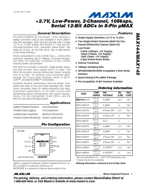
( ) ARE FOR MAX145 ONLY
µMAX/DIP
*Dice are specified at TA = +25°C, DC parameters only. **Contact factory for availability. Ordering Information continued at end of data sheet.
ELECTRICAL CHARACTERISTICS
(V DD = +2.7V to +5.25V, V REF = 2.5V, 0.1µF capacitor at REF, f SCLK = 2.17MHz, 16 clocks/conversion cycle (108ksps), CH- = GND for MAX145, TA = TMIN to TMAX, unless otherwise noted. Typical values are at TA = +25°C.) PARAMETER DC ACCURACY (Note 1) Resolution Relative Accuracy (Note 2) Differential Nonlinearity Offset Error Gain Error Gain Temperature Coefficient Channel-to-Channel Offset Matching Channel-to-Channel Gain Matching (Note 3) ±0.8 ±0.05 ±0.05 RES INL DNL MAX14_A MAX14_B No missing codes over temperature 12 ±0.5 ±1 ±0.75 ±3 ±3 Bits LSB LSB LSB LSB ppm/°C LSB LSB SYMBOL CONDITIONS MIN TYP MAX UNITS
TLC541IN;TLC541IFNR;TLC541IDW;TLC541IFN;TLC540IFN;中文规格书,Datasheet资料

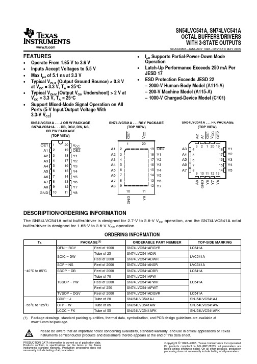
DW OR N PACKAGE (TOP VIEW)
INPUT A0 INPUT A1 INPUT A2 INPUT A3 INPUT A4 INPUT A5 INPUT A6 INPUT A7 INPUT A8 GND
8-Bit Analog-to-Digital Converter (Switched-Capacitors) 8 Output Data Register 8 8-to-1 Data Selector and Driver 16
DATA OUT
4 Self-Test Reference ADDRESS 17 INPUT I/O 18 CLOCK CS 15 4 Control Logic and I/O Counters
SLAS065B – OCTOBER 1983 – REVISED JUNE 2001
operating sequence
1 I/O CLOCK Access Cycle B (see Note C) CS MSB B3 B2 LSB B1 B0 twH(CS) Don’t Care MSB LSB Sample Cycle B 2 3 4 5 6 7 8 Don’t tconv See Note A Care Access Cycle C Sample Cycle C 1 2 3 4 5 6 7 8
Hi-Z State
MSB
NOTES: A. The conversion cycle, which requires 36 system clock periods, is initiated on the 8th falling edge of I/O CLOCK after CS goes low for the channel whose address exists in memory at that time. If CS is kept low during conversion, I/O CLOCK must remain low for at least 36 system clock cycles to allow conversion to be completed. B. The most significant bit (MSB) will automatically be placed on the DATA OUT bus after CS is brought low. The remaining seven bits (A6 – A0) will be clocked out on the first seven I/O CLOCK falling edges. C. To minimize errors caused by noise at CS, the internal circuitry waits for three system clock cycles (or less) after a chip select falling edge is detected before responding to control input signals. Therefore, no attempt should be made to clock-in address data until the minimum chip-select setup time has elapsed.
MAX485ECPA中文资料

General DescriptionThe MAX481E, MAX483E, MAX485E, MAX487E–MAX491E, and MAX1487E are low-power transceivers for RS-485 and RS-422 communications in harsh environ-ments. Each driver output and receiver input is protected against ±15kV electro-static discharge (ESD) shocks,without latchup. These parts contain one driver and one receiver. The MAX483E, MAX487E, MAX488E, and MAX489E feature reduced slew-rate drivers that minimize EMI and reduce reflections caused by improperly termi-nated cables, thus allowing error-free data transmission up to 250kbps. The driver slew rates of the MAX481E,MAX485E, MAX490E, MAX491E, and MAX1487E are not limited, allowing them to transmit up to 2.5Mbps.These transceivers draw as little as 120µA supply cur-rent when unloaded or when fully loaded with disabled drivers (see Selector Guide ). Additionally, the MAX481E,MAX483E, and MAX487E have a low-current shutdown mode in which they consume only 0.5µA. All parts oper-ate from a single +5V supply.Drivers are short-circuit current limited, and are protected against excessive power dissipation by thermal shutdown circuitry that places their outputs into a high-impedance state. The receiver input has a fail-safe feature that guar-antees a logic-high output if the input is open circuit.The MAX487E and MAX1487E feature quarter-unit-load receiver input impedance, allowing up to 128 trans-ceivers on the bus. The MAX488E–MAX491E are designed for full-duplex communications, while the MAX481E, MAX483E, MAX485E, MAX487E, and MAX1487E are designed for half-duplex applications.For applications that are not ESD sensitive see the pin-and function-compatible MAX481, MAX483, MAX485,MAX487–MAX491, and MAX1487.ApplicationsLow-Power RS-485 Transceivers Low-Power RS-422 Transceivers Level TranslatorsTransceivers for EMI-Sensitive Applications Industrial-Control Local Area NetworksNext-Generation Device Features♦For Fault-Tolerant Applications:MAX3430: ±80V Fault-Protected, Fail-Safe, 1/4-Unit Load, +3.3V, RS-485 TransceiverMAX3080–MAX3089: Fail-Safe, High-Speed (10Mbps), Slew-Rate-Limited, RS-485/RS-422Transceivers ♦For Space-Constrained Applications:MAX3460–MAX3464: +5V, Fail-Safe, 20Mbps,Profibus, RS-485/RS-422 TransceiversMAX3362: +3.3V, High-Speed, RS-485/RS-422Transceiver in a SOT23 PackageMAX3280E–MAX3284E: ±15kV ESD-Protected,52Mbps, +3V to +5.5V, SOT23, RS-485/RS-422True Fail-Safe ReceiversMAX3030E–MAX3033E: ±15kV ESD-Protected,+3.3V, Quad RS-422 Transmitters ♦For Multiple Transceiver Applications:MAX3293/MAX3294/MAX3295: 20Mbps, +3.3V,SOT23, RS-485/RS-422 Transmitters ♦For Fail-Safe Applications:MAX3440E–MAX3444E: ±15kV ESD-Protected,±60V Fault-Protected, 10Mbps, Fail-Safe RS-485/J1708 Transceivers ♦For Low-Voltage Applications:MAX3483E/MAX3485E/MAX3486E/MAX3488E/MAX3490E/MAX3491E: +3.3V Powered, ±15kV ESD-Protected, 12Mbps, Slew-Rate-Limited, True RS-485/RS-422 TransceiversMAX481E/MAX483E/MAX485E/MAX487E–MAX491E/MAX1487E±15kV ESD-Protected, Slew-Rate-Limited, Low-Power, RS-485/RS-422 Transceivers________________________________________________________________Maxim Integrated Products 1Ordering Information19-0410; Rev 4; 10/03For pricing, delivery, and ordering information,please contact Maxim/Dallas Direct!at 1-888-629-4642, or visit Maxim’s website at .Ordering Information continued at end of data sheet.Selector Guide appears at end of data sheet .M A X 481E /M A X 483E /M A X 485E /M A X 487E –M A X 491E /M A X 1487E±15kV ESD-Protected, Slew-Rate-Limited,Low-Power, RS-485/RS-422 Transceivers2_______________________________________________________________________________________Supply Voltage (V CC ) (12V)Control Input Voltage (–R —E –, DE)...................-0.5V to (V CC + 0.5V)Driver Input Voltage (DI).............................-0.5V to (V CC + 0.5V)Driver Output Voltage (Y, Z; A, B)..........................-8V to +12.5V Receiver Input Voltage (A, B).................................-8V to +12.5V Receiver Output Voltage (RO)....................-0.5V to (V CC + 0.5V)Continuous Power Dissipation (T A = +70°C)8-Pin Plastic DIP (derate 9.09mW/°C above +70°C)....727mW14-Pin Plastic DIP (derate 10.00mW/°C above +70°C)..800mW 8-Pin SO (derate 5.88mW/°C above +70°C).................471mW 14-Pin SO (derate 8.33mW/°C above +70°C)...............667mW Operating Temperature RangesMAX4_ _C_ _/MAX1487EC_ A.............................0°C to +70°C MAX4__E_ _/MAX1487EE_ A...........................-40°C to +85°C Storage Temperature Range.............................-65°C to +160°C Lead Temperature (soldering, 10sec).............................+300°CDC ELECTRICAL CHARACTERISTICS(V CC = 5V ±5%, T A = T MIN to T MAX , unless otherwise noted.) (Notes 1, 2)Stresses beyond those listed under “Absolute Maximum Ratings” may cause permanent damage to the device. These are stress ratings only, and functional operation of the device at these or any other conditions beyond those indicated in the operational sections of the specifications is not implied. Exposure to absolute maximum rating conditions for extended periods may affect device reliability.ABSOLUTE MAXIMUM RATINGSPARAMETERSYMBOL MINTYPMAX UNITS Driver Common-Mode Output VoltageV OC 3V Change in Magnitude of Driver Differential Output Voltage for Complementary Output States ∆V OD 0.2V Change in Magnitude of Driver Common-Mode Output Voltage for Complementary Output States ∆V OD 0.2V Input High Voltage V IH 2.0V Input Low Voltage V IL 0.8V Input CurrentI IN1±2µADifferential Driver Output (no load)V OD15V 2V Differential Driver Output (with load)V OD2 1.551.0-0.8mA0.25mA -0.2Receiver Differential Threshold Voltage-0.20.2V Receiver Input Hysteresis ∆V TH 70mV Receiver Output High Voltage V OH 3.5Receiver Output Low Voltage V OL 0.4V Three-State (high impedance)Output Current at ReceiverI OZR±1µA 12k ΩCONDITIONSDE = 0V;V CC = 0V or 5.25V,all devices except MAX487E/MAX1487E R = 27Ωor 50Ω, Figure 8R = 27Ωor 50Ω, Figure 8R = 27Ωor 50Ω, Figure 8DE, DI, –R —E–MAX487E/MAX1487E,DE = 0V, V CC = 0V or 5.25VDE, DI, –R —E–DE, DI, –R —E–-7V ≤V CM ≤12V V CM = 0VI O = -4mA, V ID = 200mV I O = 4mA, V ID = -200mV R = 50Ω(RS-422)0.4V ≤V O ≤2.4VR = 27Ω(RS-485), Figure 8-7V ≤V CM ≤12V, all devices except MAX487E/MAX1487EReceiver Input Resistance R IN-7V ≤V CM ≤12V, MAX487E/MAX1487E48k ΩV TH I IN2Input Current (A, B)V IN = 12V V IN = -7V V IN = 12V V IN = -7VVMAX481E/MAX483E/MAX485E/MAX487E–MAX491E/MAX1487E±15kV ESD-Protected, Slew-Rate-Limited,Low-Power, RS-485/RS-422 TransceiversSWITCHING CHARACTERISTICS—MAX481E/MAX485E, MAX490E/MAX491E, MAX1487EDC ELECTRICAL CHARACTERISTICS (continued)(V CC = 5V ±5%, T A = T MIN to T MAX , unless otherwise noted.) (Notes 1, 2)M A X 481E /M A X 483E /M A X 485E /M A X 487E –M A X 491E /M A X 1487E±15kV ESD-Protected, Slew-Rate-Limited,Low-Power, RS-485/RS-422 Transceivers4_______________________________________________________________________________________SWITCHING CHARACTERISTICS—MAX483E, MAX487E/MAX488E/MAX489E(V CC = 5V ±5%, T A = T MIN to T MAX , unless otherwise noted.) (Notes 1, 2)SWITCHING CHARACTERISTICS—MAX481E/MAX485E, MAX490E/MAX491E, MAX1487E(continued)(V CC = 5V ±5%, T A = T MIN to T MAX , unless otherwise noted.) (Notes 1, 2)2251000Figures 11 and 13, C L = 100pF, S2 closed Figures 11 and 13, C L = 100pF, S1 closed Figures 9 and 15, C L = 15pF, S2 closed,A - B = 2VCONDITIONSns 45100t ZH(SHDN)Driver Enable from Shutdown toOutput High (MAX481E)nsFigures 9 and 15, C L = 15pF, S1 closed,B - A = 2Vt ZL(SHDN)Receiver Enable from Shutdownto Output Low (MAX481E)ns 45100t ZL(SHDN)Driver Enable from Shutdown toOutput Low (MAX481E)ns 2251000t ZH(SHDN)Receiver Enable from Shutdownto Output High (MAX481E)UNITS MINTYP MAX SYMBOLPARAMETERt PLH t SKEW Figures 10 and 12, R DIFF = 54Ω,C L1= C L2= 100pFt PHL Figures 10 and 12, R DIFF = 54Ω,C L1= C L2= 100pFDriver Input to Output Driver Output Skew to Output ns 20800ns ns 2000MAX483E/MAX487E, Figures 11 and 13,C L = 100pF, S2 closedt ZH(SHDN)Driver Enable from Shutdown to Output High2502000ns2500MAX483E/MAX487E, Figures 9 and 15,C L = 15pF, S1 closedt ZL(SHDN)Receiver Enable from Shutdown to Output Lowns 2500MAX483E/MAX487E, Figures 9 and 15,C L = 15pF, S2 closedt ZH(SHDN)Receiver Enable from Shutdown to Output Highns 2000MAX483E/MAX487E, Figures 11 and 13,C L = 100pF, S1 closedt ZL(SHDN)Driver Enable from Shutdown to Output Lowns 50200600MAX483E/MAX487E (Note 5)t SHDN Time to Shutdownt PHL t PLH , t PHL < 50% of data period Figures 9 and 15, C RL = 15pF, S2 closed Figures 9 and 15, C RL = 15pF, S1 closed Figures 9 and 15, C RL = 15pF, S2 closed Figures 9 and 15, C RL = 15pF, S1 closed Figures 11 and 13, C L = 15pF, S2 closed Figures 10 and 14, R DIFF = 54Ω,C L1= C L2= 100pFFigures 11 and 13, C L = 15pF, S1 closed Figures 11 and 13, C L = 100pF, S1 closed Figures 11 and 13, C L = 100pF, S2 closed CONDITIONSkbps 250f MAX 2508002000Maximum Data Rate ns 2550t HZ Receiver Disable Time from High ns 25080020002550t LZ Receiver Disable Time from Low ns 2550t ZH Receiver Enable to Output High ns 2550t ZL Receiver Enable to Output Low ns ns 1003003000t HZ t SKD Driver Disable Time from High I t PLH - t PHL I DifferentialReceiver SkewFigures 10 and 14, R DIFF = 54Ω,C L1= C L2= 100pFns 3003000t LZ Driver Disable Time from Low ns 2502000t ZL Driver Enable to Output Low ns Figures 10 and 12, R DIFF = 54Ω,C L1= C L2= 100pFns 2502000t R , t F 2502000Driver Rise or Fall Time ns t PLH Receiver Input to Output2502000t ZH Driver Enable to Output High UNITS MIN TYP MAX SYMBOL PARAMETERMAX481E/MAX483E/MAX485E/MAX487E–MAX491E/MAX1487E±15kV ESD-Protected, Slew-Rate-Limited,Low-Power, RS-485/RS-422 Transceivers_______________________________________________________________________________________505101520253035404550OUTPUT CURRENT vs.RECEIVER OUTPUT LOW VOLTAGEM A X 481E -01OUTPUT LOW VOLTAGE (V)O U T P U T C U R R E N T (m A )1.52.02.51.00.50.10.20.30.40.50.60.70.80.9-60-2060RECEIVER OUTPUT LOW VOLTAGEvs. TEMPERATURETEMPERATURE (°C)O U T P U T L O W V O L T A G E (V )20100-4040800-5-10-15-20-251.53.0OUTPUT CURRENT vs.RECEIVER OUTPUT HIGH VOLTAGEM A X 481E -02OUTPUT HIGH VOLTAGE (V)O U T P U T C U R R E N T (m A )5.04.54.02.02.53.53.03.23.43.63.84.04.24.44.64.8-60-2060RECEIVER OUTPUT HIGH VOLTAGEvs. TEMPERATURETEMPERATURE (°C)O U T P U T H I G H V O L T A G E (V )20100-4040800102030405060708090DRIVER OUTPUT CURRENT vs. DIFFERENTIAL OUTPUT VOLTAGEM A X 481E -05DIFFERENTIAL OUTPUT VOLTAGE (V)O U T P U T C U R R E N T (m A )1.52.0 2.53.0 3.54.0 4.51.00.50__________________________________________Typical Operating Characteristics(V CC = 5V, T A = +25°C, unless otherwise noted.)NOTES FOR ELECTRICAL/SWITCHING CHARACTERISTICSNote 1:All currents into device pins are positive; all currents out of device pins are negative. All voltages are referenced to deviceground unless otherwise specified.Note 2:All typical specifications are given for V CC = 5V and T A = +25°C.Note 3:Supply current specification is valid for loaded transmitters when DE = 0V.Note 4:Applies to peak current. See Typical Operating Characteristics.Note 5:The MAX481E/MAX483E/MAX487E are put into shutdown by bringing –R —E –high and DE low. If the inputs are in this state forless than 50ns, the parts are guaranteed not to enter shutdown. If the inputs are in this state for at least 600ns, the parts are guaranteed to have entered shutdown. See Low-Power Shutdown Mode section.M A X 481E /M A X 483E /M A X 485E /M A X 487E –M A X 491E /M A X 1487E±15kV ESD-Protected, Slew-Rate-Limited,Low-Power, RS-485/RS-422 Transceivers6___________________________________________________________________________________________________________________Typical Operating Characteristics (continued)(V CC = 5V, T A = +25°C, unless otherwise noted.)1.52.32.22.12.01.91.81.71.6-60-2060DRIVER DIFFERENTIAL OUTPUT VOLTAGE vs. TEMPERATURETEMPERATURE (°C)D I F FE R E N T I A L O U T P U T V O L T A G E (V )20100-404080020406080100120140OUTPUT CURRENT vs. DRIVER OUTPUT LOW VOLTAGEM A X 481E -07OUTPUT LOW VOLTAGE (V)O U T P U T C U R R E N T (m A )246810120-10-20-30-40-50-60-70-80-90-100-8-2OUTPUT CURRENT vs. DRIVER OUTPUT HIGH VOLTAGEM A X 481E -08OUTPUT HIGH VOLTAGE (V)O U T P U T C U R R E N T (m A )642-6-400100200300400500600-60-2060MAX481E/MAX485E/MAX490E/MAX491E SUPPLY CURRENT vs. TEMPERATURETEMPERATURE (°C)S U P P L Y C U R R E N T (µA )20100-4040800100200300400500600-60-2060MAX483E/MAX487E–MAX489E SUPPLY CURRENT vs. TEMPERATURETEMPERATURE (°C)S U P P L Y C U R R E N T (µA )20100-404080100200300400500600-60-2060MAX1487ESUPPLY CURRENT vs. TEMPERATURETEMPERATURE (°C)S U P P L Y C U R R E N T (µA )20100-404080±15kV ESD-Protected, Slew-Rate-Limited, Low-Power, RS-485/RS-422 Transceivers_______________________________________________________________________________________7MAX481E/MAX483E/MAX485E/MAX487E–MAX491E/MAX1487E______________________________________________________________Pin DescriptionM A X 481E /M A X 483E /M A X 485E /M A X 487E –M A X 491E /M A X 1487E±15kV ESD-Protected, Slew-Rate-Limited,Low-Power, RS-485/RS-422 Transceivers8_________________________________________________________________________________________________Function Tables (MAX481E/MAX483E/MAX485E/MAX487E/MAX1487E) Table 1. Transmitting__________Applications Information The MAX481E/MAX483E/MAX485E/MAX487E–MAX491E and MAX1487E are low-power transceivers for RS-485 and RS-422 communications. These “E” versions of the MAX481, MAX483, MAX485, MAX487–MAX491, and MAX1487 provide extra protection against ESD. The rugged MAX481E, MAX483E, MAX485E, MAX497E–MAX491E, and MAX1487E are intended for harsh envi-ronments where high-speed communication is important. These devices eliminate the need for transient suppres-sor diodes and the associated high capacitance loading. The standard (non-“E”) MAX481, MAX483, MAX485, MAX487–MAX491, and MAX1487 are recommended for applications where cost is critical.The MAX481E, MAX485E, MAX490E, MAX491E, and MAX1487E can transmit and receive at data rates up to 2.5Mbps, while the MAX483E, MAX487E, MAX488E, and MAX489E are specified for data rates up to 250kbps. The MAX488E–MAX491E are full-duplex transceivers, while the MAX481E, MAX483E, MAX487E, and MAX1487E are half-duplex. In addition, driver-enable (DE) and receiver-enable (RE) pins are included on the MAX481E, MAX483E, MAX485E, MAX487E, MAX489E, MAX491E, and MAX1487E. When disabled, the driver and receiver outputs are high impedance.±15kV ESD Protection As with all Maxim devices, ESD-protection structures are incorporated on all pins to protect against electro-static discharges encountered during handling and assembly. The driver outputs and receiver inputs have extra protection against static electricity. Maxim’s engi-neers developed state-of-the-art structures to protect these pins against ESD of ±15kV without damage. The ESD structures withstand high ESD in all states: normal operation, shutdown, and powered down. After an ESD event, Maxim’s MAX481E, MAX483E, MAX485E, MAX487E–MAX491E, and MAX1487E keep working without latchup.ESD protection can be tested in various ways; the transmitter outputs and receiver inputs of this product family are characterized for protection to ±15kV using the Human Body Model.Other ESD test methodologies include IEC10004-2 con-tact discharge and IEC1000-4-2 air-gap discharge (for-merly IEC801-2).ESD Test Conditions ESD performance depends on a variety of conditions. Contact Maxim for a reliability report that documents test set-up, test methodology, and test results.Human Body Model Figure 4 shows the Human Body Model, and Figure 5 shows the current waveform it generates when dis-charged into a low impedance. This model consists of a 100pF capacitor charged to the ESD voltage of inter-est, which is then discharged into the test device through a 1.5kΩresistor.IEC1000-4-2 The IEC1000-4-2 standard covers ESD testing and per-formance of finished equipment; it does not specifically refer to integrated circuits (Figure 6).MAX481E/MAX483E/MAX485E/MAX487E–MAX491E/MAX1487E±15kV ESD-Protected, Slew-Rate-Limited,Low-Power, RS-485/RS-422 Transceivers_______________________________________________________________________________________9M A X 481E /M A X 483E /M A X 485E /M A X 487E –M A X 491E /M A X 1487E±15kV ESD-Protected, Slew-Rate-Limited,Low-Power, RS-485/RS-422 Transceivers10______________________________________________________________________________________Figure 8. Driver DC Test LoadFigure 9. Receiver Timing Test LoadMAX481E/MAX483E/MAX485E/MAX487E–MAX491E/MAX1487E±15kV ESD-Protected, Slew-Rate-Limited,Low-Power, RS-485/RS-422 Transceivers______________________________________________________________________________________11Figure 10. Driver/Receiver Timing Test Circuit Figure 11. Driver Timing Test LoadFigure 12. Driver Propagation DelaysFigure 13. Driver Enable and Disable Times (except MAX488E and MAX490E)Figure 14. Receiver Propagation DelaysFigure 15. Receiver Enable and Disable Times (except MAX488E and MAX490E)M A X 481E /M A X 483E /M A X 485E /M A X 487E –M A X 491E /M A X 1487E±15kV ESD-Protected, Slew-Rate-Limited,Low-Power, RS-485/RS-422 Transceivers12______________________________________________________________________________________The major difference between tests done using the Human Body Model and IEC1000-4-2 is higher peak current in IEC1000-4-2, because series resistance is lower in the IEC1000-4-2 model. Hence, the ESD with-stand voltage measured to IEC1000-4-2 is generally lower than that measured using the Human Body Model. Figure 7 shows the current waveform for the 8kV IEC1000-4-2 ESD contact-discharge test.The air-gap test involves approaching the device with a charged probe. The contact-discharge method connects the probe to the device before the probe is energized.Machine ModelThe Machine Model for ESD tests all pins using a 200pF storage capacitor and zero discharge resis-tance. Its objective is to emulate the stress caused by contact that occurs with handling and assembly during manufacturing. Of course, all pins require this protec-tion during manufacturing—not just inputs and outputs.Therefore,after PC board assembly,the Machine Model is less relevant to I/O ports.MAX487E/MAX1487E:128 Transceivers on the BusThe 48k Ω, 1/4-unit-load receiver input impedance of the MAX487E and MAX1487E allows up to 128 transceivers on a bus, compared to the 1-unit load (12k Ωinput impedance) of standard RS-485 drivers (32 transceivers maximum). Any combination of MAX487E/MAX1487E and other RS-485 transceivers with a total of 32 unit loads or less can be put on the bus. The MAX481E,MAX483E, MAX485E, and MAX488E–MAX491E have standard 12k Ωreceiver input impedance.MAX483E/MAX487E/MAX488E/MAX489E:Reduced EMI and Reflections The MAX483E and MAX487E–MAX489E are slew-rate limited, minimizing EMI and reducing reflections caused by improperly terminated cables. Figure 16shows the driver output waveform and its Fourier analy-sis of a 150kHz signal transmitted by a MAX481E,MAX485E, MAX490E, MAX491E, or MAX1487E. High-frequency harmonics with large amplitudes are evident.Figure 17 shows the same information displayed for a MAX483E, MAX487E, MAX488E, or MAX489E transmit-ting under the same conditions. Figure 17’s high-fre-quency harmonics have much lower amplitudes, and the potential for EMI is significantly reduced.Low-Power Shutdown Mode (MAX481E/MAX483E/MAX487E)A low-power shutdown mode is initiated by bringing both RE high and DE low. The devices will not shut down unless both the driver and receiver are disabled.In shutdown, the devices typically draw only 0.5µA of supply current.RE and DE may be driven simultaneously; the parts are guaranteed not to enter shutdown if RE is high and DE is low for less than 50ns. If the inputs are in this state for at least 600ns, the parts are guaranteed to enter shutdown.For the MAX481E, MAX483E, and MAX487E, the t ZH and t ZL enable times assume the part was not in the low-power shutdown state (the MAX485E, MAX488E–MAX491E, and MAX1487E can not be shut down). The t ZH(SHDN)and t ZL(SHDN)enable times assume the parts were shut down (see Electrical Characteristics ).500kHz/div0Hz5MHz 10dB/div Figure 16. Driver Output Waveform and FFT Plot ofMAX485E/MAX490E/MAX491E/MAX1487E Transmitting a 150kHz Signal500kHz/div0Hz5MHz10dB/divFigure 17. Driver Output Waveform and FFT Plot ofMAX483E/MAX487E–MAX489E Transmitting a 150kHz SignalIt takes the drivers and receivers longer to become enabled from the low-power shutdown state (t ZH(SHDN), t ZL(SHDN)) than from the operating mode (t ZH, t ZL). (The parts are in operating mode if the RE, DE inputs equal a logical 0,1 or 1,1 or 0, 0.)Driver Output Protection Excessive output current and power dissipation caused by faults or by bus contention are prevented by two mechanisms. A foldback current limit on the output stage provides immediate protection against short circuits over the whole common-mode voltage range (see Typical Operating Characteristics). In addition, a thermal shut-down circuit forces the driver outputs into a high-imped-ance state if the die temperature rises excessively.Propagation Delay Many digital encoding schemes depend on the differ-ence between the driver and receiver propagation delay times. Typical propagation delays are shown in Figures 19–22 using Figure 18’s test circuit.The difference in receiver delay times, t PLH- t PHL, is typically under 13ns for the MAX481E, MAX485E, MAX490E, MAX491E, and MAX1487E, and is typically less than 100ns for the MAX483E and MAX487E–MAX489E.The driver skew times are typically 5ns (10ns max) for the MAX481E, MAX485E, MAX490E, MAX491E, and MAX1487E, and are typically 100ns (800ns max) for the MAX483E and MAX487E–MAX489E.Typical Applications The MAX481E, MAX483E, MAX485E, MAX487E–MAX491E, and MAX1487E transceivers are designed for bidirectional data communications on multipoint bus transmission lines. Figures 25 and 26 show typical net-work application circuits. These parts can also be used as line repeaters, with cable lengths longer than 4000 feet. To minimize reflections, the line should be terminated at both ends in its characteristic impedance, and stub lengths off the main line should be kept as short as possi-ble. The slew-rate-limited MAX483E and MAX487E–MAX489E are more tolerant of imperfect termination. Bypass the V CC pin with 0.1µF.Isolated RS-485 For isolated RS-485 applications, see the MAX253 and MAX1480 data sheets.Line Length vs. Data Rate The RS-485/RS-422 standard covers line lengths up to 4000 feet. Figures 23 and 24 show the system differen-tial voltage for the parts driving 4000 feet of 26AWG twisted-pair wire at 110kHz into 100Ωloads.Figure 18. Receiver Propagation Delay Test CircuitMAX481E/MAX483E/MAX485E/MAX487E–MAX491E/MAX1487E±15kV ESD-Protected, Slew-Rate-Limited,Low-Power, RS-485/RS-422 Transceivers ______________________________________________________________________________________13M A X 481E /M A X 483E /M A X 485E /M A X 487E –M A X 491E /M A X 1487E±15kV ESD-Protected, Slew-Rate-Limited,Low-Power, RS-485/RS-422 Transceivers14______________________________________________________________________________________25ns/div 5V/divRO B A500mV/div Figure 19. MAX481E/MAX485E/MAX490E/MAX1487E Receiver t PHL25ns/div5V/div ROBA500mV/divFigure 20. MAX481E/MAX485E/MAX490E/MAX491E/MAX1487E Receiver t PLH200ns/div 5V/divRO B A500mV/div Figure 21. MAX483E/MAX487E–MAX489E Receiver t PHL200ns/div5V/div ROBA500mV/divFigure 22. MAX483E/MAX487E–MAX489E Receiver t PLH2µs/div DO 0V0V5V5V -1V 0DIV A - V BFigure 23. MAX481E/MAX485E/MAX490E/MAX491E/MAX1487E System Differential Voltage at 110kHz Driving 4000ft of Cable 2µs/divDO0V0V 5V 5V -1V1V0DIV B - V AFigure 24. MAX483E/MAX1487E–MAX489E System Differential Voltage at 110kHz Driving 4000ft of CableMAX481E/MAX483E/MAX485E/MAX487E–MAX491E/MAX1487E±15kV ESD-Protected, Slew-Rate-Limited,Low-Power, RS-485/RS-422 Transceivers______________________________________________________________________________________15Figure 26. MAX488E–MAX491E Full-Duplex RS-485 NetworkFigure 25. MAX481E/MAX483E/MAX485E/MAX487E/MAX1487E Typical Half-Duplex RS-485 NetworkM A X 481E /M A X 483E /M A X 485E /M A X 487E –M A X 491E /M A X 1487E±15kV ESD-Protected, Slew-Rate-Limited, Low-Power, RS-485/RS-422 Transceivers Maxim cannot assume responsibility for use of any circuitry other than circuitry entirely embodied in a Maxim product. No circuit patent licenses are implied. Maxim reserves the right to change the circuitry and specifications without notice at any time.16____________________Maxim Integrated Products, 120 San Gabriel Drive, Sunnyvale, CA 94086 408-737-7600©2003 Maxim Integrated ProductsPrinted USAis a registered trademark of Maxim Integrated Products.Package InformationFor the latest package outline information, go to /packages .Ordering Information (continued)Selector GuideChip InformationTRANSISTOR COUNT: 295。
LC541A中文资料
• ESD Protection Exceeds JESD 22 – 2000-V Human-Body Model (A114-A) – 200-V Machine Model (A115-A) – 1000-V Charged-Device Model (C101)
The 'LVC541A devices are ideal for driving bus lines or buffering memory address registers.
These devices feature inputs and outputs on opposite sides of the package to facilitate printed circuit board layout.
PRODUCTION DATA information is current as of publication date. Products conform to specifications per the terms of the Texas Instruments standard warranty. Production processing does not necessarily include testing of all parameters.
10
20 19 OE2 18 Y1 17 Y2 16 Y3 15 Y4 14 Y5 13 Y6 12 Y7
11
A8 GND
Y8 Y7 Y6
A3
3 2 1 20 19
4
18
Y1
A4 5
MAX487ESA中文资料
For pricing, delivery, and ordering information,please contact Maxim/Dallas Direct!at 1-888-629-4642, or visit Maxim’s website at .General DescriptionThe MAX481, MAX483, MAX485, MAX487–MAX491, and MAX1487 are low-power transceivers for RS-485 and RS-422 communication. Each part contains one driver and one receiver. The MAX483, MAX487, MAX488, and MAX489feature reduced slew-rate drivers that minimize EMI and reduce reflections caused by improperly terminated cables,thus allowing error-free data transmission up to 250kbps.The driver slew rates of the MAX481, MAX485, MAX490,MAX491, and MAX1487 are not limited, allowing them to transmit up to 2.5Mbps.These transceivers draw between 120µA and 500µA of supply current when unloaded or fully loaded with disabled drivers. Additionally, the MAX481, MAX483, and MAX487have a low-current shutdown mode in which they consume only 0.1µA. All parts operate from a single 5V supply.Drivers are short-circuit current limited and are protected against excessive power dissipation by thermal shutdown circuitry that places the driver outputs into a high-imped-ance state. The receiver input has a fail-safe feature that guarantees a logic-high output if the input is open circuit.The MAX487 and MAX1487 feature quarter-unit-load receiver input impedance, allowing up to 128 MAX487/MAX1487 transceivers on the bus. Full-duplex communi-cations are obtained using the MAX488–MAX491, while the MAX481, MAX483, MAX485, MAX487, and MAX1487are designed for half-duplex applications.________________________ApplicationsLow-Power RS-485 Transceivers Low-Power RS-422 Transceivers Level TranslatorsTransceivers for EMI-Sensitive Applications Industrial-Control Local Area Networks__Next Generation Device Features♦For Fault-Tolerant ApplicationsMAX3430: ±80V Fault-Protected, Fail-Safe, 1/4Unit Load, +3.3V, RS-485 TransceiverMAX3440E–MAX3444E: ±15kV ESD-Protected,±60V Fault-Protected, 10Mbps, Fail-Safe, RS-485/J1708 Transceivers♦For Space-Constrained ApplicationsMAX3460–MAX3464: +5V, Fail-Safe, 20Mbps,Profibus RS-485/RS-422 TransceiversMAX3362: +3.3V, High-Speed, RS-485/RS-422Transceiver in a SOT23 PackageMAX3280E–MAX3284E: ±15kV ESD-Protected,52Mbps, +3V to +5.5V, SOT23, RS-485/RS-422,True Fail-Safe ReceiversMAX3293/MAX3294/MAX3295: 20Mbps, +3.3V,SOT23, RS-855/RS-422 Transmitters ♦For Multiple Transceiver ApplicationsMAX3030E–MAX3033E: ±15kV ESD-Protected,+3.3V, Quad RS-422 Transmitters ♦For Fail-Safe ApplicationsMAX3080–MAX3089: Fail-Safe, High-Speed (10Mbps), Slew-Rate-Limited RS-485/RS-422Transceivers♦For Low-Voltage ApplicationsMAX3483E/MAX3485E/MAX3486E/MAX3488E/MAX3490E/MAX3491E: +3.3V Powered, ±15kV ESD-Protected, 12Mbps, Slew-Rate-Limited,True RS-485/RS-422 TransceiversMAX481/MAX483/MAX485/MAX487–MAX491/MAX1487Low-Power, Slew-Rate-Limited RS-485/RS-422 Transceivers______________________________________________________________Selection Table19-0122; Rev 8; 10/03Ordering Information appears at end of data sheet.M A X 481/M A X 483/M A X 485/M A X 487–M A X 491/M A X 1487Low-Power, Slew-Rate-Limited RS-485/RS-422 Transceivers 2_______________________________________________________________________________________ABSOLUTE MAXIMUM RATINGSSupply Voltage (V CC ).............................................................12V Control Input Voltage (RE , DE)...................-0.5V to (V CC + 0.5V)Driver Input Voltage (DI).............................-0.5V to (V CC + 0.5V)Driver Output Voltage (A, B)...................................-8V to +12.5V Receiver Input Voltage (A, B).................................-8V to +12.5V Receiver Output Voltage (RO).....................-0.5V to (V CC +0.5V)Continuous Power Dissipation (T A = +70°C)8-Pin Plastic DIP (derate 9.09mW/°C above +70°C)....727mW 14-Pin Plastic DIP (derate 10.00mW/°C above +70°C)..800mW 8-Pin SO (derate 5.88mW/°C above +70°C).................471mW14-Pin SO (derate 8.33mW/°C above +70°C)...............667mW 8-Pin µMAX (derate 4.1mW/°C above +70°C)..............830mW 8-Pin CERDIP (derate 8.00mW/°C above +70°C).........640mW 14-Pin CERDIP (derate 9.09mW/°C above +70°C).......727mW Operating Temperature RangesMAX4_ _C_ _/MAX1487C_ A...............................0°C to +70°C MAX4__E_ _/MAX1487E_ A.............................-40°C to +85°C MAX4__MJ_/MAX1487MJA...........................-55°C to +125°C Storage Temperature Range.............................-65°C to +160°C Lead Temperature (soldering, 10sec).............................+300°CDC ELECTRICAL CHARACTERISTICS(V CC = 5V ±5%, T A = T MIN to T MAX , unless otherwise noted.) (Notes 1, 2)Stresses beyond those listed under “Absolute Maximum Ratings” may cause permanent damage to the device. These are stress ratings only, and functional operation of the device at these or any other conditions beyond those indicated in the operational sections of the specifications is not implied. Exposure to absolute maximum rating conditions for extended periods may affect device reliability.V V IN = -7VV IN = 12V V IN = -7V V IN = 12V Input Current (A, B)I IN2V TH k Ω48-7V ≤V CM ≤12V, MAX487/MAX1487R INReceiver Input Resistance -7V ≤V CM ≤12V, all devices except MAX487/MAX1487R = 27Ω(RS-485), Figure 40.4V ≤V O ≤2.4VR = 50Ω(RS-422)I O = 4mA, V ID = -200mV I O = -4mA, V ID = 200mV V CM = 0V-7V ≤V CM ≤12V DE, DI, RE DE, DI, RE MAX487/MAX1487,DE = 0V, V CC = 0V or 5.25VDE, DI, RE R = 27Ωor 50Ω, Figure 4R = 27Ωor 50Ω, Figure 4R = 27Ωor 50Ω, Figure 4DE = 0V;V CC = 0V or 5.25V,all devices except MAX487/MAX1487CONDITIONSk Ω12µA ±1I OZRThree-State (high impedance)Output Current at ReceiverV 0.4V OL Receiver Output Low Voltage 3.5V OH Receiver Output High Voltage mV 70∆V TH Receiver Input Hysteresis V -0.20.2Receiver Differential Threshold Voltage-0.2mA 0.25mA-0.81.01.55V OD2Differential Driver Output (with load)V 2V 5V OD1Differential Driver Output (no load)µA±2I IN1Input CurrentV 0.8V IL Input Low Voltage V 2.0V IH Input High Voltage V 0.2∆V OD Change in Magnitude of Driver Common-Mode Output Voltage for Complementary Output States V 0.2∆V OD Change in Magnitude of Driver Differential Output Voltage for Complementary Output States V 3V OC Driver Common-Mode Output VoltageUNITS MINTYPMAX SYMBOL PARAMETERMAX481/MAX483/MAX485/MAX487–MAX491/MAX1487Low-Power, Slew-Rate-Limited RS-485/RS-422 Transceivers_______________________________________________________________________________________3SWITCHING CHARACTERISTICS—MAX481/MAX485, MAX490/MAX491, MAX1487(V CC = 5V ±5%, T A = T MIN to T MAX , unless otherwise noted.) (Notes 1, 2)DC ELECTRICAL CHARACTERISTICS (continued)(V CC = 5V ±5%, T A = T MIN to T MAX , unless otherwise noted.) (Notes 1, 2)ns 103060t PHLDriver Rise or Fall Time Figures 6 and 8, R DIFF = 54Ω, C L1= C L2= 100pF ns MAX490M, MAX491M MAX490C/E, MAX491C/E2090150MAX481, MAX485, MAX1487MAX490M, MAX491MMAX490C/E, MAX491C/E MAX481, MAX485, MAX1487Figures 6 and 8, R DIFF = 54Ω,C L1= C L2= 100pF MAX481 (Note 5)Figures 5 and 11, C RL = 15pF, S2 closedFigures 5 and 11, C RL = 15pF, S1 closed Figures 5 and 11, C RL = 15pF, S2 closed Figures 5 and 11, C RL = 15pF, S1 closed Figures 6 and 10, R DIFF = 54Ω,C L1= C L2= 100pFFigures 6 and 8,R DIFF = 54Ω,C L1= C L2= 100pF Figures 6 and 10,R DIFF = 54Ω,C L1= C L2= 100pF CONDITIONS ns 510t SKEW ns50200600t SHDNTime to ShutdownMbps 2.5f MAX Maximum Data Rate ns 2050t HZ Receiver Disable Time from High ns 103060t PLH 2050t LZ Receiver Disable Time from Low ns 2050t ZH Driver Input to Output Receiver Enable to Output High ns 2050t ZL Receiver Enable to Output Low 2090200ns ns 134070t HZ t SKD Driver Disable Time from High |t PLH - t PHL |DifferentialReceiver Skewns 4070t LZ Driver Disable Time from Low ns 4070t ZL Driver Enable to Output Low 31540ns51525ns 31540t R , t F 2090200Driver Output Skew to Output t PLH , t PHL Receiver Input to Output4070t ZH Driver Enable to Output High UNITS MIN TYP MAX SYMBOL PARAMETERFigures 7 and 9, C L = 100pF, S2 closed Figures 7 and 9, C L = 100pF, S1 closed Figures 7 and 9, C L = 15pF, S1 closed Figures 7 and 9, C L = 15pF, S2 closedM A X 481/M A X 483/M A X 485/M A X 487–M A X 491/M A X 1487Low-Power, Slew-Rate-Limited RS-485/RS-422 Transceivers 4_______________________________________________________________________________________SWITCHING CHARACTERISTICS—MAX483, MAX487/MAX488/MAX489(V CC = 5V ±5%, T A = T MIN to T MAX , unless otherwise noted.) (Notes 1, 2)SWITCHING CHARACTERISTICS—MAX481/MAX485, MAX490/MAX491, MAX1487 (continued)(V CC = 5V ±5%, T A = T MIN to T MAX , unless otherwise noted.) (Notes 1, 2)3001000Figures 7 and 9, C L = 100pF, S2 closed Figures 7 and 9, C L = 100pF, S1 closed Figures 5 and 11, C L = 15pF, S2 closed,A - B = 2VCONDITIONSns 40100t ZH(SHDN)Driver Enable from Shutdown toOutput High (MAX481)nsFigures 5 and 11, C L = 15pF, S1 closed,B - A = 2Vt ZL(SHDN)Receiver Enable from Shutdownto Output Low (MAX481)ns 40100t ZL(SHDN)Driver Enable from Shutdown toOutput Low (MAX481)ns 3001000t ZH(SHDN)Receiver Enable from Shutdownto Output High (MAX481)UNITS MINTYP MAX SYMBOLPARAMETERt PLH t SKEW Figures 6 and 8, R DIFF = 54Ω,C L1= C L2= 100pFt PHL Figures 6 and 8, R DIFF = 54Ω,C L1= C L2= 100pFDriver Input to Output Driver Output Skew to Output ns 100800ns ns 2000MAX483/MAX487, Figures 7 and 9,C L = 100pF, S2 closedt ZH(SHDN)Driver Enable from Shutdown to Output High2502000ns2500MAX483/MAX487, Figures 5 and 11,C L = 15pF, S1 closedt ZL(SHDN)Receiver Enable from Shutdown to Output Lowns 2500MAX483/MAX487, Figures 5 and 11,C L = 15pF, S2 closedt ZH(SHDN)Receiver Enable from Shutdown to Output Highns 2000MAX483/MAX487, Figures 7 and 9,C L = 100pF, S1 closedt ZL(SHDN)Driver Enable from Shutdown to Output Lowns 50200600MAX483/MAX487 (Note 5) t SHDN Time to Shutdownt PHL t PLH , t PHL < 50% of data period Figures 5 and 11, C RL = 15pF, S2 closed Figures 5 and 11, C RL = 15pF, S1 closed Figures 5 and 11, C RL = 15pF, S2 closed Figures 5 and 11, C RL = 15pF, S1 closed Figures 7 and 9, C L = 15pF, S2 closed Figures 6 and 10, R DIFF = 54Ω,C L1= C L2= 100pFFigures 7 and 9, C L = 15pF, S1 closed Figures 7 and 9, C L = 100pF, S1 closed Figures 7 and 9, C L = 100pF, S2 closed CONDITIONSkbps 250f MAX 2508002000Maximum Data Rate ns 2050t HZ Receiver Disable Time from High ns 25080020002050t LZ Receiver Disable Time from Low ns 2050t ZH Receiver Enable to Output High ns 2050t ZL Receiver Enable to Output Low ns ns 1003003000t HZ t SKD Driver Disable Time from High I t PLH - t PHL I DifferentialReceiver SkewFigures 6 and 10, R DIFF = 54Ω,C L1= C L2= 100pFns 3003000t LZ Driver Disable Time from Low ns 2502000t ZL Driver Enable to Output Low ns Figures 6 and 8, R DIFF = 54Ω,C L1= C L2= 100pFns 2502000t R , t F 2502000Driver Rise or Fall Time ns t PLH Receiver Input to Output2502000t ZH Driver Enable to Output High UNITS MIN TYP MAX SYMBOL PARAMETERMAX481/MAX483/MAX485/MAX487–MAX491/MAX1487Low-Power, Slew-Rate-Limited RS-485/RS-422 Transceivers_______________________________________________________________________________________530002.5OUTPUT CURRENT vs.RECEIVER OUTPUT LOW VOLTAGE525M A X 481-01OUTPUT LOW VOLTAGE (V)O U T P U T C U R R E N T (m A )1.515100.51.02.0203540450.90.1-50-252575RECEIVER OUTPUT LOW VOLTAGE vs.TEMPERATURE0.30.7TEMPERATURE (°C)O U T P U TL O W V O L T A G E (V )500.50.80.20.60.40100125-20-41.5 2.0 3.0 5.0OUTPUT CURRENT vs.RECEIVER OUTPUT HIGH VOLTAGE-8-16M A X 481-02OUTPUT HIGH VOLTAGE (V)O U T P U T C U R R E N T (m A )2.5 4.0-12-18-6-14-10-203.54.5 4.83.2-50-252575RECEIVER OUTPUT HIGH VOLTAGE vs.TEMPERATURE3.64.4TEMPERATURE (°C)O U T P UT H I G H V O L T A G E (V )0504.04.63.44.23.83.01001259000 1.0 3.0 4.5DRIVER OUTPUT CURRENT vs.DIFFERENTIAL OUTPUT VOLTAGE1070M A X 481-05DIFFERENTIAL OUTPUT VOLTAGE (V)O U T P U T C U R R E N T (m A )2.0 4.05030806040200.5 1.5 2.53.5 2.31.5-50-2525125DRIVER DIFFERENTIAL OUTPUT VOLTAGEvs. TEMPERATURE1.72.1TEMPERATURE (°C)D I F FE R E N T I A L O U T P U T V O L T A G E (V )751.92.21.62.01.8100502.4__________________________________________Typical Operating Characteristics(V CC = 5V, T A = +25°C, unless otherwise noted.)NOTES FOR ELECTRICAL/SWITCHING CHARACTERISTICSNote 1:All currents into device pins are positive; all currents out of device pins are negative. All voltages are referenced to deviceground unless otherwise specified.Note 2:All typical specifications are given for V CC = 5V and T A = +25°C.Note 3:Supply current specification is valid for loaded transmitters when DE = 0V.Note 4:Applies to peak current. See Typical Operating Characteristics.Note 5:The MAX481/MAX483/MAX487 are put into shutdown by bringing RE high and DE low. If the inputs are in this state for lessthan 50ns, the parts are guaranteed not to enter shutdown. If the inputs are in this state for at least 600ns, the parts are guaranteed to have entered shutdown. See Low-Power Shutdown Mode section.M A X 481/M A X 483/M A X 485/M A X 487–M A X 491/M A X 1487Low-Power, Slew-Rate-Limited RS-485/RS-422 Transceivers 6___________________________________________________________________________________________________________________Typical Operating Characteristics (continued)(V CC = 5V, T A = +25°C, unless otherwise noted.)120008OUTPUT CURRENT vs.DRIVER OUTPUT LOW VOLTAGE20100M A X 481-07OUTPUT LOW VOLTAGE (V)O U T P U T C U R R E N T (m A )6604024801012140-1200-7-5-15OUTPUT CURRENT vs.DRIVER OUTPUT HIGH VOLTAGE-20-80M A X 481-08OUTPUT HIGH VOLTAGE (V)O U T P U T C U R R E N T (m A )-31-603-6-4-2024-100-40100-40-60-2040100120MAX1487SUPPLY CURRENT vs. TEMPERATURE300TEMPERATURE (°C)S U P P L Y C U R R E N T (µA )20608050020060040000140100-50-2550100MAX481/MAX485/MAX490/MAX491SUPPLY CURRENT vs. TEMPERATURE300TEMPERATURE (°C)S U P P L Y C U R R E N T (µA )257550020060040000125100-50-2550100MAX483/MAX487–MAX489SUPPLY CURRENT vs. TEMPERATURE300TEMPERATURE (°C)S U P P L Y C U R R E N T (µA )257550020060040000125MAX481/MAX483/MAX485/MAX487–MAX491/MAX1487Low-Power, Slew-Rate-Limited RS-485/RS-422 Transceivers_______________________________________________________________________________________7______________________________________________________________Pin DescriptionFigure 1. MAX481/MAX483/MAX485/MAX487/MAX1487 Pin Configuration and Typical Operating CircuitM A X 481/M A X 483/M A X 485/M A X 487–M A X 491/M A X 1487__________Applications InformationThe MAX481/MAX483/MAX485/MAX487–MAX491 and MAX1487 are low-power transceivers for RS-485 and RS-422 communications. The MAX481, MAX485, MAX490,MAX491, and MAX1487 can transmit and receive at data rates up to 2.5Mbps, while the MAX483, MAX487,MAX488, and MAX489 are specified for data rates up to 250kbps. The MAX488–MAX491 are full-duplex trans-ceivers while the MAX481, MAX483, MAX485, MAX487,and MAX1487 are half-duplex. In addition, Driver Enable (DE) and Receiver Enable (RE) pins are included on the MAX481, MAX483, MAX485, MAX487, MAX489,MAX491, and MAX1487. When disabled, the driver and receiver outputs are high impedance.MAX487/MAX1487:128 Transceivers on the BusThe 48k Ω, 1/4-unit-load receiver input impedance of the MAX487 and MAX1487 allows up to 128 transceivers on a bus, compared to the 1-unit load (12k Ωinput impedance) of standard RS-485 drivers (32 trans-ceivers maximum). Any combination of MAX487/MAX1487 and other RS-485 transceivers with a total of 32 unit loads or less can be put on the bus. The MAX481/MAX483/MAX485 and MAX488–MAX491 have standard 12k ΩReceiver Input impedance.Low-Power, Slew-Rate-Limited RS-485/RS-422 Transceivers 8_______________________________________________________________________________________Figure 2. MAX488/MAX490 Pin Configuration and Typical Operating CircuitFigure 3. MAX489/MAX491 Pin Configuration and Typical Operating CircuitMAX483/MAX487/MAX488/MAX489:Reduced EMI and ReflectionsThe MAX483 and MAX487–MAX489 are slew-rate limit-ed, minimizing EMI and reducing reflections caused by improperly terminated cables. Figure 12 shows the dri-ver output waveform and its Fourier analysis of a 150kHz signal transmitted by a MAX481, MAX485,MAX490, MAX491, or MAX1487. High-frequency har-monics with large amplitudes are evident. Figure 13shows the same information displayed for a MAX483,MAX487, MAX488, or MAX489 transmitting under the same conditions. Figure 13’s high-frequency harmonics have much lower amplitudes, and the potential for EMI is significantly reduced.MAX481/MAX483/MAX485/MAX487–MAX491/MAX1487Low-Power, Slew-Rate-Limited RS-485/RS-422 Transceivers_______________________________________________________________________________________9_________________________________________________________________Test CircuitsFigure 4. Driver DC Test Load Figure 5. Receiver Timing Test LoadFigure 6. Driver/Receiver Timing Test Circuit Figure 7. Driver Timing Test LoadM A X 481/M A X 483/M A X 485/M A X 487–M A X 491/M A X 1487Low-Power, Slew-Rate-Limited RS-485/RS-422 Transceivers 10_______________________________________________________Switching Waveforms_________________Function Tables (MAX481/MAX483/MAX485/MAX487/MAX1487)Figure 8. Driver Propagation DelaysFigure 9. Driver Enable and Disable Times (except MAX488 and MAX490)Figure 10. Receiver Propagation DelaysFigure 11. Receiver Enable and Disable Times (except MAX488and MAX490)Table 1. TransmittingTable 2. ReceivingLow-Power Shutdown Mode (MAX481/MAX483/MAX487)A low-power shutdown mode is initiated by bringing both RE high and DE low. The devices will not shut down unless both the driver and receiver are disabled.In shutdown, the devices typically draw only 0.1µA of supply current.RE and DE may be driven simultaneously; the parts are guaranteed not to enter shutdown if RE is high and DE is low for less than 50ns. If the inputs are in this state for at least 600ns, the parts are guaranteed to enter shutdown.For the MAX481, MAX483, and MAX487, the t ZH and t ZL enable times assume the part was not in the low-power shutdown state (the MAX485/MAX488–MAX491and MAX1487 can not be shut down). The t ZH(SHDN)and t ZL(SHDN)enable times assume the parts were shut down (see Electrical Characteristics ).It takes the drivers and receivers longer to become enabled from the low-power shutdown state (t ZH(SHDN ), t ZL(SHDN)) than from the operating mode (t ZH , t ZL ). (The parts are in operating mode if the –R —E –,DE inputs equal a logical 0,1 or 1,1 or 0, 0.)Driver Output ProtectionExcessive output current and power dissipation caused by faults or by bus contention are prevented by two mechanisms. A foldback current limit on the output stage provides immediate protection against short cir-cuits over the whole common-mode voltage range (see Typical Operating Characteristics ). In addition, a ther-mal shutdown circuit forces the driver outputs into a high-impedance state if the die temperature rises excessively.Propagation DelayMany digital encoding schemes depend on the differ-ence between the driver and receiver propagation delay times. Typical propagation delays are shown in Figures 15–18 using Figure 14’s test circuit.The difference in receiver delay times, | t PLH - t PHL |, is typically under 13ns for the MAX481, MAX485,MAX490, MAX491, and MAX1487 and is typically less than 100ns for the MAX483 and MAX487–MAX489.The driver skew times are typically 5ns (10ns max) for the MAX481, MAX485, MAX490, MAX491, and MAX1487, and are typically 100ns (800ns max) for the MAX483 and MAX487–MAX489.MAX481/MAX483/MAX485/MAX487–MAX491/MAX1487Low-Power, Slew-Rate-Limited RS-485/RS-422 Transceivers______________________________________________________________________________________1110dB/div0Hz5MHz500kHz/div10dB/div0Hz5MHz500kHz/divFigure 12. Driver Output Waveform and FFT Plot of MAX481/MAX485/MAX490/MAX491/MAX1487 Transmitting a 150kHz SignalFigure 13. Driver Output Waveform and FFT Plot of MAX483/MAX487–MAX489 Transmitting a 150kHz SignalM A X 481/M A X 483/M A X 485/M A X 487–M A X 491/M A X 1487Low-Power, Slew-Rate-Limited RS-485/RS-422 Transceivers 12______________________________________________________________________________________V CC = 5V T A = +25°CV CC = 5V T A = +25°CV CC = 5V T A = +25°CV CC = 5V T A = +25°CFigure 14. Receiver Propagation Delay Test CircuitFigure 15. MAX481/MAX485/MAX490/MAX491/MAX1487Receiver t PHLFigure 16. MAX481/MAX485/MAX490/MAX491/MAX1487Receiver t PLHPHL Figure 18. MAX483, MAX487–MAX489 Receiver t PLHLine Length vs. Data RateThe RS-485/RS-422 standard covers line lengths up to 4000 feet. For line lengths greater than 4000 feet, see Figure 23.Figures 19 and 20 show the system differential voltage for the parts driving 4000 feet of 26AWG twisted-pair wire at 110kHz into 120Ωloads.Typical ApplicationsThe MAX481, MAX483, MAX485, MAX487–MAX491, and MAX1487 transceivers are designed for bidirectional data communications on multipoint bus transmission lines.Figures 21 and 22 show typical network applications circuits. These parts can also be used as line repeaters, with cable lengths longer than 4000 feet, as shown in Figure 23.To minimize reflections, the line should be terminated at both ends in its characteristic impedance, and stub lengths off the main line should be kept as short as possi-ble. The slew-rate-limited MAX483 and MAX487–MAX489are more tolerant of imperfect termination.MAX481/MAX483/MAX485/MAX487–MAX491/MAX1487Low-Power, Slew-Rate-Limited RS-485/RS-422 Transceivers______________________________________________________________________________________13DIV Y -V ZRO5V 0V1V0V -1V5V 0V2µs/divFigure 19. MAX481/MAX485/MAX490/MAX491/MAX1487 System Differential Voltage at 110kHz Driving 4000ft of Cable Figure 20. MAX483, MAX487–MAX489 System Differential Voltage at 110kHz Driving 4000ft of CableFigure 21. MAX481/MAX483/MAX485/MAX487/MAX1487 Typical Half-Duplex RS-485 NetworkM A X 481/M A X 483/M A X 485/M A X 487–M A X 491/M A X 1487Low-Power, Slew-Rate-Limited RS-485/RS-422 Transceivers 14______________________________________________________________________________________Figure 22. MAX488–MAX491 Full-Duplex RS-485 NetworkFigure 23. Line Repeater for MAX488–MAX491Isolated RS-485For isolated RS-485 applications, see the MAX253 and MAX1480 data sheets.MAX481/MAX483/MAX485/MAX487–MAX491/MAX1487Low-Power, Slew-Rate-Limited RS-485/RS-422 Transceivers______________________________________________________________________________________15_______________Ordering Information_________________Chip TopographiesMAX481/MAX483/MAX485/MAX487/MAX1487N.C. RO 0.054"(1.372mm)0.080"(2.032mm)DE DIGND B N.C.V CCARE * Contact factory for dice specifications.__Ordering Information (continued)M A X 481/M A X 483/M A X 485/M A X 487–M A X 491/M A X 1487Low-Power, Slew-Rate-Limited RS-485/RS-422 Transceivers 16______________________________________________________________________________________TRANSISTOR COUNT: 248SUBSTRATE CONNECTED TO GNDMAX488/MAX490B RO 0.054"(1.372mm)0.080"(2.032mm)N.C. DIGND Z A V CCYN.C._____________________________________________Chip Topographies (continued)MAX489/MAX491B RO 0.054"(1.372mm)0.080"(2.032mm)DE DIGND Z A V CCYREMAX481/MAX483/MAX485/MAX487–MAX491/MAX1487Low-Power, Slew-Rate-Limited RS-485/RS-422 Transceivers______________________________________________________________________________________17Package Information(The package drawing(s) in this data sheet may not reflect the most current specifications. For the latest package outline information go to /packages .)S O I C N .E P SM A X 481/M A X 483/M A X 485/M A X 487–M A X 491/M A X 1487Low-Power, Slew-Rate-Limited RS-485/RS-422 Transceivers 18______________________________________________________________________________________Package Information (continued)(The package drawing(s) in this data sheet may not reflect the most current specifications. For the latest package outline information go to /packages .)MAX481/MAX483/MAX485/MAX487–MAX491Low-Power, Slew-Rate-Limited RS-485/RS-422 TransceiversMaxim cannot assume responsibility for use of any circuitry other than circuitry entirely embodied in a Maxim product. No circuit patent licenses are implied. Maxim reserves the right to change the circuitry and specifications without notice at any time.Maxim Integrated Products, 120 San Gabriel Drive, Sunnyvale, CA 94086 408-737-7600 ____________________19©2003 Maxim Integrated ProductsPrinted USAis a registered trademark of Maxim Integrated Products.M A X 481/M A X 483/M A X 485/M A X 487–M A X 491/M A X 1487P D I P N .E PSPackage Information (continued)(The package drawing(s) in this data sheet may not reflect the most current specifications. For the latest package outline information go to /packages .)。
MAX490EEPA中文资料
元器件交易网
MAX481E/MAX483E/MAX485E/MAX487E–MAX491E/MAX1487E
19-0410; Rev 4; 10/03
±15kV ESD-Protected, Slew-Rate-Limited, Low-Power, RS-485/RS-422 Transceivers
Ordering Information
PART MAX481ECPA MAX481ECSA MAX481EEPA MAX481EESA MAX483ECPA MAX483ECSA MAX483EEPA MAX483EESA
TEMP RANGE 0°C to +70°C 0°C to +70°C -40°C to +85°C -40°C to +85°C 0°C to +70°C 0°C to +70°C -40°C to +85°C -40°C to +85°C
MAX4090中文资料

MIN TYP MAX
2.7
5.5
6.5
10
6.5
10
0.15
1
0.27 0.38 0.47
VCLP
1.45
22.5
35
3
1.9
2
2.1
60
80
2.55
2.7
4.3
4.6
VCLP 0.47
45
85
40
85
110
VCC x 0.3
VCC x 0.7
0.003
1
4
2
UNITS V
mA
µA V V µA MΩ V/V dB
Note 1: VCLP is the input clamp voltage as defined in the DC Electrical Characteristics table.
Stresses beyond those listed under “Absolute Maximum Ratings” may cause permanent damage to the device. These are stress ratings only, and functional operation of the device at these or any other conditions beyond those indicated in the operational sections of the specifications is not implied. Exposure to absolute maximum rating conditions for extended periods may affect device reliability.
- 1、下载文档前请自行甄别文档内容的完整性,平台不提供额外的编辑、内容补充、找答案等附加服务。
- 2、"仅部分预览"的文档,不可在线预览部分如存在完整性等问题,可反馈申请退款(可完整预览的文档不适用该条件!)。
- 3、如文档侵犯您的权益,请联系客服反馈,我们会尽快为您处理(人工客服工作时间:9:00-18:30)。
General DescriptionThe MAX5417/MAX5418/MAX5419 nonvolatile, linear-taper, digital potentiometers perform the function of a mechanical potentiometer, but replace the mechanics with a simple 2-wire digital interface, allowing communi-cation with multiple devices. Each device performs the same function as a discrete potentiometer or variable resistor and has 256 tap points.The devices feature an internal, nonvolatile EEPROM used to store the wiper position for initialization during power-up. The fast-mode I 2C™-compatible serial inter-face allows communication at data rates up to 400kbps,minimizing board space and reducing interconnection complexity in many applications. Each device is available with one of four factory-preset addresses (see the Selector Guide ) and features an address input for a total of eight unique address combinations.The MAX5417/MAX5418/MAX5419 provide three nomi-nal resistance values: 50k Ω(MAX5417), 100k Ω(MAX5418), or 200k Ω(MAX5419). The nominal resistor temperature coefficient is 35ppm/°C end-to-end, and only 5ppm/°C ratiometric. This makes the devices ideal for applications requiring a low-temperature-coefficient variable resistor, such as low-drift, programmable gain-amplifier circuit configurations.The MAX5417/MAX5418/MAX5419 are available in a 3mm x 3mm 8-pin TDF N package, and are specified over the extended -40°C to +85°C temperature range.ApplicationsMechanical Potentiometer Replacement Low-Drift Programmable-Gain Amplifiers Volume ControlLiquid-Crystal Display (LCD) Contrast ControlFeatures♦Power-On Recall of Wiper Position from Nonvolatile Memory♦Tiny 3mm x 3mm 8-Pin TDFN Package♦35ppm/°C End-to-End Resistance Temperature Coefficient♦5ppm/°C Ratiometric Temperature Coefficient ♦50k Ω/100k Ω/200k ΩResistor Values ♦Fast I 2C-Compatible Serial Interface ♦500nA (typ) Static Supply Current♦Single-Supply Operation: +2.7V to +5.25V ♦256 Tap Positions♦±0.5 LSB DNL in Voltage-Divider Mode ♦±0.5 LSB INL in Voltage-Divider ModeMAX5417/MAX5418/MAX5419256-Tap, Nonvolatile, I 2C-Interface,Digital Potentiometers________________________________________________________________Maxim Integrated Products1Ordering Information/Selector GuideFunctional Diagram19-3185; Rev 2; 8/04For pricing, delivery, and ordering information,please contact Maxim/Dallas Direct!at 1-888-629-4642, or visit Maxim’s website at .Pin Configuration appears at end of data sheet.I 2C is a trademark of Phillips Corp.Purchase of I 2C components from Maxim Integrated Products,Inc. or one of its sublicensed Associated Companies, conveys a license under the Philips I 2C Patent Rights to use these com-ponents in an I 2C system, provided that the system conforms to the I 2C Standard Specification as defined by Philips.**Exposed pad.M A X 5417/M A X 5418/M A X 5419256-Tap, Nonvolatile, I 2C-Interface, Digital PotentiometersABSOLUTE MAXIMUM RATINGSELECTRICAL CHARACTERISTICSStresses beyond those listed under “Absolute Maximum Ratings” may cause permanent damage to the device. These are stress ratings only, and functional operation of the device at these or any other conditions beyond those indicated in the operational sections of the specifications is not implied. Exposure to absolute maximum rating conditions for extended periods may affect device reliability.V DD to GND...........................................................-0.3V to +6.0V All Other Pins to GND.................................-0.3V to (V DD + 0.3V)Maximum Continuous Current into H, L, and WMAX5417......................................................................±1.3mA MAX5418......................................................................±0.6mA MAX5419......................................................................±0.3mAContinuous Power Dissipation (T A = +70°C)8-Pin TDFN (derate 24.4mW/°C above +70°C).........1951mW Operating Temperature Range ...........................-40°C to +85°C Junction Temperature......................................................+150°C Storage Temperature Range.............................-60°C to +150°C Lead Temperature (soldering, 10s).................................+300°CMAX5417/MAX5418/MAX5419256-Tap, Nonvolatile, I 2C-Interface,Digital Potentiometers_______________________________________________________________________________________3ELECTRICAL CHARACTERISTICS (continued)(V DD = +2.7V to +5.25V, H = V DD , L = GND, T A = -40°C to +85°C, unless otherwise noted. Typical values are at V DD = +5V, T A = +25°C.)TIMING CHARACTERISTICS(V = +2.7V to +5.25V, H = V , L = GND, T = -40°C to +85°C, unless otherwise noted. Typical values are at V = +5V, T =M A X 5417/M A X 5418/M A X 5419256-Tap, Nonvolatile, I 2C-Interface, Digital Potentiometers 4_______________________________________________________________________________________wiper terminal is unloaded and measured with a high-input-impedance voltmeter.Note 2:The DNL and INL are measured with the potentiometer configured as a variable resistor. H is unconnected and L = GND.For the 5V condition, the wiper terminal is driven with a source current of 80µA for the 50k Ωconfiguration, 40µA for the 100k Ωconfiguration, and 20µA for the 200k Ωconfiguration. For the 3V condition, the wiper terminal is driven with a source current of 40µA for the 50k Ωconfiguration, 20µA for the 100k Ωconfiguration, and 10µA for the 200k Ωconfiguration.Note 3:The wiper resistance is measured using the source currents given in Note 2. For operation to V DD = 2.7V, see WiperResistance vs. Temperature in the Typical Operating Characteristics.Note 4:The device draws higher supply current when the digital inputs are driven with voltages between (V DD - 0.5V) and (GND +0.5V). See Supply Current vs. Digital Input Voltage in the Typical Operating Characteristics.Note 5:Wiper at midscale with a 10pF load (DC measurement). L = GND; an AC source is applied to H; and the W output is mea-sured. A 3dB bandwidth occurs when the AC W/H value is 3dB lower than the DC W/H value.Note 6:The programming current operates only during power-up and NV writes.Note 7:SCL clock period includes rise and fall times t R and t F . All digital input signals are specified with t R = t F = 2ns and timedfrom a voltage level of (V IL + V IH ) / 2.Note 8:Wiper settling time is the worst-case 0% to 50% rise time measured between consecutive wiper positions. H = V DD ,L = GND, and the wiper terminal is unloaded and measured with a 10pF oscilloscope probe (see the Typical Operating Characteristics for the tap-to-tap switching transient).Note 9:An appropriate bus pullup resistance must be selected depending on board capacitance. Refer to the document linked tothis web address: /acrobat/literature/9398/39340011.pdf.Note 10:The idle time begins from the initiation of the stop pulse.TIMING CHARACTERISTICS (continued)(V DD = +2.7V to +5.25V, H = V DD , L = GND, T A = -40°C to +85°C, unless otherwise noted. Typical values are at V DD = +5V, T A =MAX5417/MAX5418/MAX5419256-Tap, Nonvolatile, I 2C-Interface,Digital Potentiometers_______________________________________________________________________________________5WIPER TRANSIENT AT POWER-ONW 1V/divV DD 2V/div4µs/divC L = 10pF TAP = 128H = V DDEND-TO-END RESISTANCE % CHANGEvs. TEMPERATURETEMPERATURE (°C)E N D -T O -E N D R E S I S T A N C E % C H A N G E603510-15-0.8-0.6-0.4-0.200.20.40.60.81.0-1.0-4085DNL vs. TAP POSITIONTAP POSITION R E S I S T A N C E D N L (L S B )224192160128966432-0.20-0.15-0.10-0.0500.100.200.050.150.25-0.25256TAP POSITION R E S I S T A N C E I N L (L S B )224192160128966432-0.20-0.15-0.10-0.0500.100.200.050.150.25-0.250256INL vs. TAP POSITIONWIPER RESISTANCE vs. TAP POSITIONTAP POSITIONR E S I S T A N C E (Ω)2241921601289664321002003004005006007000256Typical Operating Characteristics(V DD = +5V, T A = +25°C, unless otherwise noted.)STANDBY SUPPLY CURRENTvs. TEMPERATUREM A X 5417 t o c 06TEMPERATURE (°C)S T A N D B Y S U P P L Y C U R R E N T (µA )603510-150.20.40.60.81.00-4085WIPER RESISTANCE vs. TEMPERATURETEMPERATURE (°C)R E S I S T A N C E (Ω)603510-151002003004005006007000-4085M A X 5417/M A X 5418/M A X 5419256-Tap, Nonvolatile, I 2C-Interface, Digital Potentiometers 6SUPPLY CURRENTvs. DIGITAL INPUT VOLTAGEM A X 5417 t o c 08DIGITAL INPUT VOLTAGE (V)S U P P L Y C U R R E N T (µA )432110020030040050060000510k 1k 1000.0010.010.11101000.000110100kTHD+N RESPONSEFREQUENCY (Hz)T H D +N (%)INL vs. TAP POSITION(MAX5417)TAP POSITIONR E S I S T A N C E I N L (L S B )224192160128966432-0.500.51.01.52.02.53.0-1.0256Typical Operating Characteristics (continued)(V DD = +5V, T A = +25°C, unless otherwise noted.)MAX5417/MAX5418/MAX5419256-Tap, Nonvolatile, I 2C-Interface,Digital Potentiometers_______________________________________________________________________________________7-0.2-0.100.10.20.3-0.3DNL vs. TAP POSITION(MAX5419)TAP POSITION D N L (L S B )2241923264961281600256MIDSCALE WIPER RESPONSE vs. FREQUENCY(MAX5417)FREQUENCY (kHz)W I P E R R E S P O N S E (d B )10010-25-20-10-15-50-3011000MIDSCALE WIPER RESPONSE vs. FREQUENCY(MAX5418)FREQUENCY (kHz)W I P E R R E S P O N S E (d B )10010-25-20-10-15-50-3011000MIDSCALE WIPER RESPONSE vs. FREQUENCY(MAX5419)FREQUENCY (kHz)W I P E R R E S P O N S E (d B )10010-40-35-30-25-20-15-10-50-4511000TAP-TO-TAP SWITCHING TRANSIENT(MAX5417)W10mV/divSDA 2V/div1µs/divMAX5417C L = 10pF FROM TAP 127TO TAP 128H = V DDTAP-TO-TAP SWITCHING TRANSIENT(MAX5418)W10mV/divSDA 2V/div 1µs/divMAX5418C L = 10pF FROM TAP 127TO TAP 128H = V DDTAP-TO-TAP SWITCHING TRANSIENT(MAX5419)W10mV/divSDA 2V/div 1µs/divMAX5419C L = 10pF FROM TAP 127TO TAP 128H = V DDTypical Operating Characteristics (continued)(V DD = +5V, T A = +25°C, unless otherwise noted.)M A X 5417/M A X 5418/M A X 5419256-Tap, Nonvolatile, I 2C-Interface, Digital Potentiometers 8_______________________________________________________________________________________Detailed DescriptionThe MAX5417/MAX5418/MAX5419 contain a resistor array with 255 resistive elements. The MAX5417 has a total end-to-end resistance of 50k Ω, the MAX5418 has an end-to-end resistance of 100k Ω, and the MAX5419has an end-to-end resistance of 200k Ω. The MAX5417/MAX5418/MAX5419 allow access to the high,low, and wiper terminals for a standard voltage-divider configuration. H, L, and W can be connected in any desired configuration as long as their voltages fall between GND and V DD .A simple 2-wire I 2C-compatible serial interface moves the wiper among the 256 tap points. A nonvolatile mem-ory stores the wiper position and recalls the stored wiper position in the nonvolatile memory upon power-up. The nonvolatile memory is guaranteed for 50 years for wiper data retention and up to 200,000 wiper store cycles.Figure 1. I 2C Serial-Interface Timing DiagramFigure 2. Load CircuitMAX5417/MAX5418/MAX5419256-Tap, Nonvolatile, I 2C-Interface,Digital Potentiometers_______________________________________________________________________________________9Analog CircuitryThe MAX5417/MAX5418/MAX5419 consist of a resistor array with 255 resistive elements; 256 tap points are accessible to the wiper, W, along the resistor string between H and L. The wiper tap point is selected by programming the potentiometer through the 2-wire (I 2C)interface. Eight data bits, an address byte, and a con-trol byte program the wiper position. The H and L termi-nals of the MAX5417/MAX5418/MAX5419 are similar to the two end terminals of a mechanical potentiometer.The MAX5417/MAX5418/MAX5419 feature power-on reset circuitry that loads the wiper position from non-volatile memory at power-up.Digital InterfaceThe MAX5417/MAX5418/MAX5419 feature an internal,nonvolatile EEPROM that stores the wiper state for ini-tialization during power-up. The shift register decodes the control and address bits, routing the data to the proper memory registers. Data can be written to a volatile memory register, immediately updating the wiper position, or data can be written to a nonvolatile register for storage.The volatile register retains data as long as the device is powered. Once power is removed, the volatile regis-ter is cleared. The nonvolatile register retains data even after power is removed. Upon power-up, the power-on reset circuitry controls the transfer of data from the non-volatile register to the volatile register.Serial AddressingThe MAX5417/MAX5418/MAX5419 operate as a slave that receives data through an I 2C- and SMBus™-com-patible 2-wire interface. The interface uses a serial data access (SDA) line and a serial clock line (SCL) to achieve communication between master(s) and slave(s). A master, typically a microcontroller, initiates all data transfers to the MAX5417/MAX5418/MAX5419,and generates the SCL clock that synchronizes the data transfer (Figure 1).The MAX5417/MAX5418/MAX5419 SDA line operates as both an input and an open-drain output. A pullup resistor, typically 4.7k Ω, is required on the SDA bus.The MAX5417/MAX5418/MAX5419 SCL operates only as an input. A pullup resistor, typically 4.7k Ω, is required on the SCL bus if there are multiple masters on the 2-wire interface, or if the master in a single-mas-ter system has an open-drain SCL output.Each transmission consists of a START (S) condition (F igure 3) sent by a master, followed by the MAX5417/MAX5418/MAX5419 7-bit slave address plus the 8th bit (Figure 4), 1 command byte (Figure 7) and 1data byte, and finally a STOP (P) condition (Figure 3).Start and Stop ConditionsBoth SCL and SDA remain high when the interface is not busy. A master signals the beginning of a transmis-sion with a START condition by transitioning SDA from high to low while SCL is high. When the master has fin-ished communicating with the slave, it issues a STOP condition by transitioning the SDA from low to high while SCL is high. The bus is then free for another transmission (Figure 3).Bit TransferOne data bit is transferred during each clock pulse.The data on the SDA line must remain stable while SCL is high (Figure 5).Figure 3. Start and Stop ConditionsSMBus is a trademark of Intel Corporation.M A X 5417/M A X 5418/M A X 5419256-Tap, Nonvolatile, I 2C-Interface, Digital Potentiometers 10______________________________________________________________________________________AcknowledgeThe acknowledge bit is a clocked 9th bit that the recipient uses to handshake receipt of each byte of data (F igure 6). Thus, each byte transferred effectively requires 9 bits.The master generates the 9th clock pulse, and the recipi-ent pulls down SDA during the acknowledge clock pulse,so the SDA line is stable low during the high period of the clock pulse. When the master transmits to the MAX5417/MAX5418/MAX5419, the devices generate the acknowledge bit because the MAX5417/MAX5418/MAX5419 are the recipients.Slave AddressThe MAX5417/MAX5418/MAX5419 have a 7-bit-long slave address (F igure 4). The 8th bit following the 7-bitslave address is the NOP/W bit. Set the NOP/W bit low for a write command and high for a no-operation command.The MAX5417/MAX5418/MAX5419 are available in one of four possible slave addresses (Table 1). The first 4bits (MSBs) of the MAX5417/MAX5418/MAX5419 slave addresses are always 0101. The next 2 bits are factory programmed (see Table 1). Connect the A0 input to either GND or V DD to toggle between two unique device addresses for a part. Each device must have a unique address to share the bus. Therefore, a maxi-mum of eight MAX5417/MAX5418/MAX5419 devices can share the same bus.Table 1. MAX5417/MAX5418/MAX5419 Address CodesFigure 5. Bit Transfer Figure 6. AcknowledgeMAX5417/MAX5418/MAX5419Digital Potentiometers______________________________________________________________________________________11Message Format for WritingA write to the MAX5417/MAX5418/MAX5419 consists of the transmission of the device’s slave address with the 8th bit set to zero, followed by at least 1 byte of infor-mation (F igure 7). The 1st byte of information is the command byte. The bytes received after the command byte are the data bytes. The 1st data byte goes into the internal register of the MAX5417/MAX5418/MAX5419 as selected by the command byte (Figure 8).Command ByteUse the command byte to select the source and desti-nation of the wiper data (nonvolatile or volatile memory registers) and swap data between nonvolatile and volatile memory registers (see Table 2).Command DescriptionsVREG:The data byte writes to the volatile memory reg-ister and the wiper position updates with the data in the volatile memory register.NVREG:The data byte writes to the nonvolatile memo-ry register. The wiper position is unchanged.NVREGxVREG:Data transfers from the nonvolatile memory register to the volatile memory register (wiper position updates).VREGxNVREG:Data transfers from the volatile memo-ry register into the nonvolatile memory register.Figure 7. Command Byte ReceivedFigure 8. Command and Single Data Byte ReceivedM A X 5417/M A X 5418/M A X 5419Digital Potentiometers 12______________________________________________________________________________________Nonvolatile MemoryThe internal EEPROM consists of an 8-bit nonvolatile register that retains the value written to it before the device is powered down. The nonvolatile register is programmed with the midscale value at the factory.Power-UpUpon power-up, the MAX5417/MAX5418/MAX5419load the data stored in the nonvolatile memory register into the volatile memory register, updating the wiper position with the data stored in the nonvolatile memory register. This initialization period takes 10µs.StandbyThe MAX5417/MAX5418/MAX5419 feature a low-power standby. When the device is not being programmed, it goes into standby mode and power consumption is typically 500nA.Applications InformationThe MAX5417/MAX5418/MAX5419 are intended for cir-cuits requiring digitally controlled adjustable resis-tance, such as LCD contrast control (where voltage biasing adjusts the display contrast), or for programma-ble filters with adjustable gain and/or cutoff frequency.Positive LCD Bias ControlF igures 9 and 10 show an application where the volt-age-divider or variable resistor is used to make an adjustable, positive LCD bias voltage. The op amp pro-vides buffering and gain to the resistor-divider network made by the potentiometer (F igure 9) or to a fixed resistor and a variable resistor (see Figure 10).Programmable FilterF igure 11 shows the configuration for a 1st-order pro-grammable filter. The gain of the filter is adjusted by R2, and the cutoff frequency is adjusted by R3. Use the following equations to calculate the gain (G) and the 3dB cutoff frequency (f C ):Figure 9. Positive LCD Bias Control Using a Voltage-Divider Figure 10. Positive LCD Bias Control Using a Variable ResistorAdjustable Voltage ReferenceFigure 12 shows the MAX5417/MAX5418/MAX5419 used as the feedback resistors in multiple adjustable voltage-reference applications. Independently adjust the output voltage of the MAX6160 from 1.23V to V IN - 0.2V by changing the wiper positions of the MAX5417/MAX5418/MAX5419.Offset Voltage and Gain AdjustmentConnect the high and low terminals of one potentiometer of a MAX5417 between the NULL inputs of a MAX410and the wiper to the op amp’s positive supply to nullify the offset voltage over the operating temperature range.Install the other potentiometer in the feedback path to adjust the gain of the MAX410 (see Figure 13).MAX5417/MAX5418/MAX5419Digital Potentiometers______________________________________________________________________________________13Figure 13. Offset Voltage and Gain Adjustment CircuitPin ConfigurationChip InformationTRANSISTOR COUNT: 4637PROCESS: BiCMOSM A X 5417/M A X 5418/M A X 5419Digital Potentiometers 14______________________________________________________________________________________Package Information(The package drawing(s) in this data sheet may not reflect the most current specifications. For the latest package outline information go to /packages .)Maxim cannot assume responsibility for use of any circuitry other than circuitry entirely embodied in a Maxim product. No circuit patent licenses are implied. Maxim reserves the right to change the circuitry and specifications without notice at any time.Maxim Integrated Products, 120 San Gabriel Drive, Sunnyvale, CA 94086 408-737-7600 ____________________15©2004 Maxim Integrated Products Printed USA is a registered trademark of Maxim Integrated Products.MAX5417/MAX5418/MAX5419。