24.5% e$ciency PERT silicon solar cells on SEH-1
Amorphous silicon solar cell-非晶硅基太阳能电池

非晶硅维基百科,自由百科全书文章:硅薄膜电池非晶硅(a-Si或α-Si)是硅同素异形体的非结晶形式。
它可以作为很多低温薄膜材料的基底,为各种电子材料提供一些独特的功能。
内容■1描述■2非晶硅和碳■3应用■3.1太阳能电池■3.1.1微晶硅和Micromorphous硅■3.1.2大型生产■4参见■5参考■6外部链接1.描述晶体硅的晶包是一个正四面体结构,每个硅原子与四个离其最近的硅原子相连组成一个正四面体结构。
这个四面体结构,在晶体硅中周期排布,从而形成一个有序的晶格。
非晶硅,大范围内碳原子不是周期有序的排列。
相反,原子形成一个连续的随机网络。
由于碳原子无序排列的性质,使一些原子有一个悬空的氢键。
这些悬挂氢键代表着连续随机网络的缺陷,可能会导致异常的电子性能。
如果需要,可钝化材料的悬挂氢键,悬挂氢键密度可以降低几个数量级。
钝化的非晶硅(a –Si:H)有足够低的缺陷,可以使用。
但是不幸的是,悬挂氢键是光致降解材料,被称为Staebler Wronski效应。
2.非晶硅和碳硅和碳的非晶合金(无定形硅碳化物,氢化,a-Si1-xCx:H)是一个有趣的变种。
碳原子的引入,为材料性能的可控性额外增加了控制的自由度。
可见光可以透过这种薄膜。
碳浓度的增加,合金中的电子传导带和价带(也称为“光学带隙”和带隙)之间的差距扩大。
这有可能增加非晶碳化硅层太阳能电池的光效。
另一方面,随着碳原子浓度在硅碳非晶合金中的增加,使原子网络结构更混乱,这增加了半导体材料的电子迁移率,这对半导体材料的性能是不利的。
在几篇科学文献中发现,主要是受电子器件的质量因素影响,但是制备非晶碳化硅的商用设备还很缺乏。
3.应用虽然非晶硅比单晶硅的电子性能低,但是它的实际应用更加灵活。
例如,非晶硅比单晶硅制造简单,所以价格较低,从而降低了硅原材料的成本。
一个更大的优势是可以在非常低的温度,如低达75摄氏度沉积非晶硅(a-Si)。
这使得它不仅可以在玻璃上沉积,还可以成功的应用滚动对滚动加工技术使其与塑料相结合。
染料敏化太阳能电池材料

理论研究
25
染料敏化太阳能电池领域发展了二十多年,虽然至今没有实现大规模的应用,还是带动了一系列学科的发展。近几年相关领域论文数目出现大幅度下降,不少研究者也纷纷转向其他方向。尽管有人对染料敏化太阳能电池发展前景存疑,但仍旧有部分课题组坚持着相关研究,特别是固态染料敏化太阳能电池方向。
(一)镜面型散射材料
理论研究
18
(二)空心型散射材料
理论研究
19
(三)多功能的复合型散射材料
PARTFOUR
理论研究
21
对电极在染料敏化太阳能电池中主要担负电解质中离子的还原,使电解质中的氧化还原电对处于平衡状态。为了使碘三离子的还原反应顺利地进行,需要采用具有一定催化活性的材料来作为对电极。
PART ONE
PART TWO
PART THREE
太阳能因其清洁无污染、储量巨大、不受地域限制等优点一直被认为是最有潜力的新能源
研究背景
5
PART FOUR
太阳能电池的发展最早可以追溯到年法国的在液体电解质中发现的光生伏特效应,他以涂有氧化铜或鹵化银的金属电极浸入稀电解质溶液中,在光照的条件下产生电流。随后用硒做出了实际的太阳能电池,但一直到20世纪中期,虽经各方努力,硒只能将太阳光的1%左右转换为电能,因此并没有实用化的器件产生。直到年美国实验室的和首次制备了转换效率为的6%单晶硅太阳能电池,揭开了太阳能电池应用的序幕。在随后的数十年时间里,非晶硅、非晶硅薄膜、砷化镓、硫化镉、铜铟镓硒、有机聚合物和染料敏化等各类太阳能电池相继被研发出来。
出自: Advanced Materials, 2016, DOI: 10.1002/adma.201602382
PARTSIX
4 Design of Silicon Solar Cells

§4.1 Basic Cell Design §4.1 基础太阳能电池设计
The second factor is that the high theoretical efficiency predictions assume a high concentration ratio, 第二个因素是假设入射光有高聚光 比, Assuming that temperature and resistive effects do not dominate in a concentrator solar cell, 并假设温度和电阻效应对聚光太阳 能电池的影响很小。
For silicon solar cells, 对于硅太阳能电池来说, a more realistic efficiency under one sun operation is about 26 to 28%. 在一个太阳照射下,比较实际的理论最高效率值大约为26%-28%。 The maximum efficiency measured for a silicon solar cell is currently 24.7% under AM1.5G. 现今实验室测得的硅太阳能电池的最高效率为24.7%。 4
3)minimizing the forward bias dark current; 尽量减小正偏压下暗电流。
4)extracting the current from the cell without resistive losses. 提取不受电阻损耗的电流。
7
§4.2 Optical Losses §4.2 光学损失
1)To minimize top contact coverage 减小顶电极覆盖面积
2)To use anti-reflection coatings 在电池表面铺上减反射膜 3)Surface texturing 表面制绒
crystalline silicon solar cells
1 0 -2
'
I
'
O 280 D 300 A 320 + 340
K K K K
+At:lo
1 0 -4
+At3(3 +,5~O
f
, I ,
÷~ ,_~
%
0 10.6
o
0
O
?
0.5 1.0
10-8
i
[
I
-1.0
-0.5
0.0
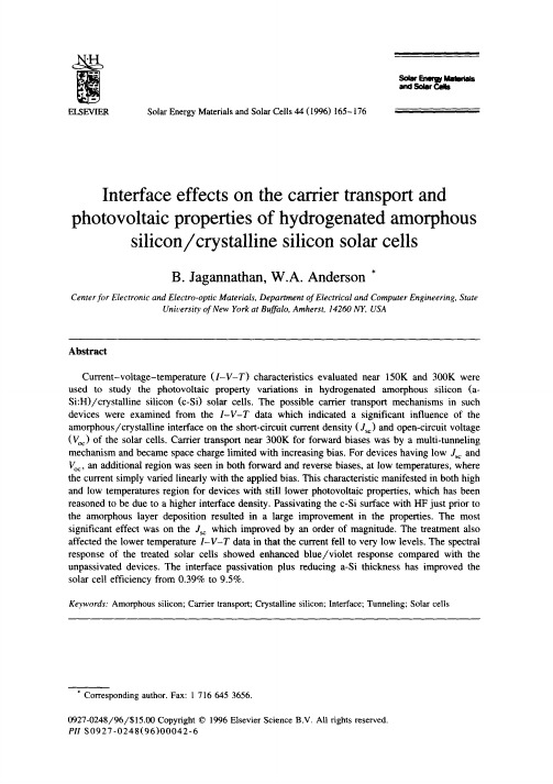
Voltage (volts) Fig. 1. ( a ) I - V - T characteristics of n + a-Si/i (0.6 Ixm) a-Si/p c-Si solar cell near 300K, (b) Saturation current density versus 1 / T for characteristics in Fig. la.
Keywords: Amorphoussilicon; Carrier transport;Crystallinesilicon; Interface;Tunneling;Solar cells
* Correspondingauthor. Fax: 1 716 645 3656. 0927-0248/96/$15.00 Copyright © 1996 Elsevier Science B.V. All rights reserved. PH S0927-0248(96)00042-6
s*~r r:nm~ ~
• na S ~ r oals
ELSEVIER
Solar Energy Materials and Solar Cells 44 (1996) 165-176
Solar cell efficiency tables (Version 38)
RESEARCH:SHORT COMMUNICATION:ACCELERATED PUBLICATIONSolar cell efficiency tables(Version38)Martin A.Green1*,Keith Emery2,Yoshihiro Hishikawa3,Wilhelm Warta4and Ewan D.Dunlop5 1ARC Photovoltaics Centre of Excellence,University of New South Wales,Sydney2052,Australia2National Renewable Energy Laboratory,1617Cole Boulevard,Golden,CO80401,USA3National Institute of Advanced Industrial Science and Technology(AIST),Research Center for Photovoltaics(RCPV),Central2, Umezono1-1-1,Tsukuba,Ibaraki305-8568,Japan4Fraunhofer-Institute for Solar Energy Systems,Department of Solar Cells–Materials and Technology,Heidenhofstr.2,D-79110 Freiburg,Germany5European Commission–Joint Research Centre,Renewable Energy Unit,Institute for Energy,Via E.Fermi2749,IT-21027Ispra (VA),ItalyABSTRACTConsolidated tables showing an extensive listing of the highest independently confirmed efficiencies for solar cells and modules are presented.Guidelines for inclusion of results into these tables are outlined and new entries since January,2011 are reviewed.Copyright#2011John Wiley&Sons,Ltd.KEYWORDSsolar cell efficiency;photovoltaic efficiency;energy conversion efficiency*CorrespondenceMartin A.Green,ARC Photovoltaics Centre of Excellence,University of New South Wales,Sydney2052,Australia.E-mail:m.green@.auReceived23May20111.INTRODUCTIONSince January,1993,‘‘Progress in Photovoltaics’’has published six monthly listings of the highest confirmed efficiencies for a range of photovoltaic cell and module technologies[1–3].By providing guidelines for the inclusion of results into these tables,this not only provides an authoritative summary of the current state-of-the-art but also encourages researchers to seek independent confir-mation of results and to report results on a standardized basis.In a recent version of these Tables(Version33)[2], results were updated to the new internationally accepted reference spectrum(IEC60904-3,Ed.2,2008),where this was possible.The most important criterion for inclusion of results into the Tables is that they must have been measured by a recognized test centre listed elsewhere[1].A distinction is made between three different eligible areas:total area, aperture area,and designated illumination area[1].‘‘Active area’’efficiencies are not included.There are also certain minimum values of the area sought for the different device types(above0.05cm2for a con-centrator cell,1cm2for a1-sun cell,and800cm2for a module)[1].Results are reported for cells and modules made from different semiconductors and for sub-categories within each semiconductor grouping(e.g.,crystalline,polycrys-talline,and thinfilm).From Version36onwards,spectral response information is included when available in the form of a plot of the external quantum efficiency(EQE) versus wavelength,normalized to the peak measured value. Starting from the present version,current–voltage(IV) curves will also be included when possible.2.NEW RESULTSHighest confirmed‘‘one sun’’cell and module results are reported in Tables I and II.Any changes in the Tables from those previously published[3]are set in bold type.In most cases,a literature reference is provided that describes either the result reported or a similar result.Table I summarizes the best measurements for cells and sub-modules while Table II shows the best results for modules. Table III contains what might be described as‘‘notable exceptions.’’While not conforming to the requirements to be recognized as a class record,the cells and modules in this Table have notable characteristics that will be ofPROGRESS IN PHOTOVOLTAICS:RESEARCH AND APPLICATIONSProg.Photovolt:Res.Appl.2011;19:565–572Published online in Wiley Online Library().DOI:10.1002/pip.1150 Copyrightß2011John Wiley&Sons,Ltd.565Table I.Confirmed terrestrial cell and submodule efficiencies measured under the global AM1.5spectrum(1000W/m2)at258C(IEC60904-3:2008,ASTM G-173-03global).Classification a Effic.b(%)Area c(cm2)V oc(V)J sc(mA/cm2)FF d(%)Test Centre e(and date)DescriptionSiliconSi(crystalline)25.0Æ0.5 4.00(da)0.70642.7f82.8Sandia(3/99)g UNSW PERL[13]Si(multicrystalline)20.4Æ0.5 1.002(ap)0.66438.080.9NREL(5/04)g FhG-ISE[14]Si(thinfilm transfer)19.1W0.4 3.983(ap)0.65037.8h77.6FhG-ISE(2/11)ISFH(43m m thick)[4]Si(thinfilm submodule)10.5Æ0.394.0(ap)0.492i29.7i72.1FhG-ISE(8/07)g CSG Solar(1–2m mon glass;20cells)[15]III–V cellsGaAs(thinfilm)28.1W0.80.998(ap) 1.11129.4h85.9NREL(3/11)Alta Devices[5]GaAs(multicrystalline)18.4Æ0.5 4.011(t)0.99423.279.7NREL(11/95)g RTI,Ge substrate[16]InP(crystalline)22.1Æ0.7 4.02(t)0.87829.585.4NREL(4/90)g Spire,epitaxial[17]Thinfilm chalcogenideCIGS(cell)19.6Æ0.6j0.996(ap)0.71334.8k79.2NREL(4/09)NREL,CIGS on glass[18] CIGS(submodule)16.7Æ0.416.0(ap)0.661i33.6i75.1FhG-ISE(3/00)g U.Uppsala,4serial cells[19] CdTe(cell)16.7Æ0.5j 1.032(ap)0.84526.175.5NREL(9/01)g NREL,mesa on glass[20] Amorphous/nanocrystalline SiSi(amorphous)10.1Æ0.3l 1.036(ap)0.88616.75f67.0NREL(7/09)Oerlikon Solar Lab,Neuchatel[21]Si(nanocrystalline)10.1Æ0.2m 1.199(ap)0.53924.476.6JQA(12/97)Kaneka(2m m on glass)[22] PhotochemicalDye-sensitized10.9W0.3n 1.008(da)0.73621.7h68.0AIST(1/11)Sharp[6]Dye-sensitized(submodule)9.9Æ0.4n17.11(ap)0.719i19.4i,k71.4AIST(8/10)Sony,eight parallel cells[23] OrganicOrganic polymer8.3Æ0.3n 1.031(ap)0.81614.46k70.2NREL(11/10)Konarka[24]Organic(submodule) 3.5Æ0.3n208.4(ap)8.6200.84748.3NREL(7/09)Solarmer[25]Multijunction devicesGaInP/GaAs/Ge32.0Æ1.5m 3.989(t) 2.62214.3785.0NREL(1/03)Spectrolab(monolithic) GaAs/CIS(thinfilm)25.8Æ1.3m 4.00(t)–––NREL(11/89)Kopin/Boeing(fourterminal)[26]a-Si/nc-Si/nc-Si(thinfilm)12.4W0.7o 1.050(ap) 1.9368.9671.5NREL(3/11)United Solar[7]a-Si/nc-Si(thinfilm cell)11.9Æ0.8p 1.227(ap) 1.34612.92k68.5NREL(8/10)Oerlikon Solar Lab,Neuchatel[27]a-Si/nc-Si(thinfilmsubmodule)11.7Æ0.4m,q14.23(ap) 5.462 2.9971.3AIST(9/04)Kaneka(thinfilm)[28] Organic(two-cell tandem)8.3Æ0.3n 1.087(ap) 1.7338.03k59.5FhG-ISE(10/10)Heliatek[29]a CIGS,CuInGaSe2;a-Si,amorphous silicon/hydrogen alloy.b Effic.,efficiency.c(ap),aperture area;(t),total area;(da),designated illumination area.d FF,fill factor.e FhG-ISE,Fraunhofer Institut fu¨r Solare Energiesysteme;JQA,Japan Quality Assurance;AIST,Japanese National Institute of Advanced Industrial Science and Technology.f Spectral response reported in Version36of these Tables.g Recalibrated from original measurement.h Spectral response and current-voltage curve reported in present version of these Tables.i Reported on a‘‘per cell’’basis.j Not measured at an external laboratory.k Spectral response reported in Version37of these Tables.l Light soaked at Oerlikon prior to testing at NREL(1000h,1sun,508C).m Measured under IEC60904-3Ed.1:1989reference spectrum.n Stability not investigated.Refs.[30,31]review the stability of similar devices.o Light soaked under100mW/cm2white light at508C for over1000h.p Stabilized by1000h,1sun illumination at a sample temperature of508C.q Stabilized by174h,1sun illumination after20h,5sun illumination at a sample temperature of508C.566Prog.Photovolt:Res.Appl.2011;19:565–572ß2011John Wiley&Sons,Ltd.DOI:10.1002/pip Solar cell efficiency tables M.A.Green et al.Table II.Confirmed terrestrial module efficiencies measured under the global AM1.5spectrum(1000W/m2)at a cell temperature of258C(IEC60904-3:2008,ASTM G-173-03global).Classification a Effic.b(%)Area c(cm2)V oc(V)I sc(A)FF d(%)Test Centre(and date)DescriptionSi(crystalline)22.9Æ0.6778(da) 5.60 3.9780.3Sandia(9/96)e UNSW/Gochermann[32] Si(large crystalline)21.4Æ0.615780(ap)68.6 6.29378.4NREL(10/09)SunPower[33]Si(multicrystalline)17.8W0.414920(ap)38.869.04f75.7ESTI(2/11)Q-Cells(60serial cells)[8] Si(thin-film polycrystalline)8.2Æ0.2661(ap)25.00.32068.0Sandia(7/02)e Pacific Solar(1–2m m on glass)[34] GaAs(crystalline)21.1W0.6921(ap)12.69 1.98f77.1NREL(4/11)Alta Devices[5]CIGS15.7Æ0.59703(ap)28.247.254g72.5NREL(11/10)Miasole[35]CIGSS(Cd free)13.5Æ0.73459(ap)31.2 2.1868.9NREL(8/02)e Showa Shell[36]CdTe12.8W0.46687(ap)94.1 1.2771.4NREL(1/11)PrimeStar monolithic[9] a-Si/a-SiGe/a-SiGe(tandem)10.4Æ0.5h,i905(ap) 4.353 3.28566.0NREL(10/98)e USSC[37]a CIGSS,CuInGaSSe;a-Si,amorphous silicon/hydrogen alloy;a-SiGe,amorphous silicon/germanium/hydrogen alloy.b Effic.,efficiency.c(ap),aperture area;(da),designated illumination area.d FF,fill factor.e Recalibrated from original measurement.f Spectral response and current–voltage curve reported in present version of these Tables.g Spectral response reported in Version37of these Tables.h Light soaked at NREL for1000h at508C,nominally1-sun illumination.i Measured under IEC60904-3Ed.1:1989reference spectrum.Table III.‘‘Notable Exceptions’’:‘‘Top ten’’confirmed cell and module results,not class records measured under the global AM1.5 spectrum(1000W/m2)at258C(IEC60904-3:2008,ASTM G-173-03global).Classification a Effic.b(%)Area c(cm2)V oc(V)J sc(mA/cm2)FF(%)Test Centre(and date)DescriptionCells(silicon)Si(MCZ crystalline)24.7Æ0.5 4.0(da)0.70442.083.5Sandia(7/99)d UNSW PERL,SEH MCZsubstrate[38]Si(large crystalline)24.2Æ0.7155.1(t)0.72140.5e82.9NREL(5/10)Sunpower n-type CZsubstrate[39]Si(large crystalline)23.0Æ0.6100.4(t)0.72939.680.0AIST(2/09)Sanyo HIT,n-typesubstrate[40]Si(large multicrystalline)19.5W0.4242.7(t)0.65239.0f76.7FhG ISE(3/11)Q-Cells,laserfired contacts[8]Cells(others)GaInP/GaAs/GaInAs(tandem)35.8Æ1.50.880(ap) 3.01213.985.3AIST(9/09)Sharp,monolithic[41] CIGS(thinfilm)20.3Æ0.60.5015(ap)0.74035.4e77.5FhG-ISE(6/10)ZSW Stuttgart,CIGS on glass[42]CZTSS(thinfilm)9.7W0.30.4362(ap)0.51628.6f65.4NREL(8/09)IBM solution grown[10]a-Si/nc-Si/nc-Si(tandem)12.5Æ0.7g0.27(da) 2.0109.1168.4NREL(3/09)United Solar stabilized[43] Dye-sensitized11.2Æ0.3h0.219(ap)0.73621.072.2AIST(3/06)d Sharp[44]Luminescent submodule7.1Æ0.2h25(ap) 1.0088.84e79.5ESTI(9/08)ECN Petten,GaAs cells[45] a CIGS,CuInGaSe2;CZTSS,Cu2ZnSnS4Ày Se y.b Effic.,efficiency.c(ap),aperture area;(t),total area;(da),designated illumination area.d Recalibrated from original measurement.e Spectral response reported in Version37of these Tables.f Spectral response and current-voltage curve reported in the present version of these Tables.g Light soaked under100mW/cm2white light at508C for1000h.h Stability not investigated.Prog.Photovolt:Res.Appl.2011;19:565–572ß2011John Wiley&Sons,Ltd. DOI:10.1002/pip 567M.A.Green et al.Solar cell efficiency tablesinterest to sections of the photovoltaic community,with entries based on their significance and timeliness.To ensure discrimination,Table III is limited to nominally10entries with the present authors having voted for their preferences for inclusion.Readers who have suggestions of results for inclusion into this Table are welcome to contact any of the authors with full details. Suggestions conforming to the guidelines will be included on the voting list for a future issue.Table IV shows the best results for concentrator cells and concentrator modules(a smaller number of‘‘notable exceptions’’for concentrator cells and modules addition-ally is included in Table IV).Ten new results are reported in the present version of these Tables.Thefirst new result in Table I is for a layer transfer, 43m m thick silicon solar cell with19.1%efficiency measured for a4cm2cell fabricated by the Institute for Solar Energy Research,Hamelin(ISFH)[4]and measured by the Fraunhofer Institute for Solar Energy Systems(FhG-ISE),representing a large improvement on the previously best result of16.7%for a cell of this type.The second new result in Table I is an outright record for solar conversion by any single-junction photovoltaic device,following on from the27.6%result reported in the previous version of these Tables[3].An efficiency of 28.1%has been measured at the National Renewable Energy Laboratory(NREL)for a1cm2thin-film GaAs device fabricated by Alta Devices,Inc.Alta Devices is a Santa Clara based‘‘start-up’’seeking to develop low-cost, 30%efficient solar modules[5].A third new result in Table I is for a dye-sensitized cell with efficiency of10.9%reported for a1cm2cell fabricated by Sharp[6]and measured by the Japanese National Institute of Advanced Industrial Science and Technology(AIST).Thefinal new result in Table I is for a small area (1.05cm2)triple junction amorphous/nanocrystalline sili-con solar cell(a-Si/nc-Si/nc-Si)fabricated by United Solar (USlr)[7]where a stabilized efficiency of12.4%has been measured by NREL.Following a vigorous burst of activity in the multi-crystalline silicon module area reported in the three previous versions of these Tables,wherefive groups exceeded the previous record for module efficiency over an 18month period,one of these groups has done even better. In Table II,a new efficiency record of17.8%is reported fora large(1.5m2aperture area)module fabricated by Q-Cells[8]and measured by the European Solar Test Installation, Ispra(ESTI).Also reported in Table II is a record result for a thin-film GaAs module,with an efficiency of21.1%reported for a 0.92m2module fabricated by Alta Devices[5]and measured by NREL.With the recent improvement in GaAs cell performance reported in Table I,this efficiency might also be expected to improve rapidly in the future.Table IV.Terrestrial concentrator cell and module efficiencies measured under the ASTM G-173-03direct beam AM1.5spectrum ata cell temperature of258C.Classification Effic.a(%)Area b(cm2)Intensity c(suns)Test Centre(and date)DescriptionSingle CellsGaAs29.1Æ1.3d,e0.0505(da)117FhG-ISE(3/10)Fraunhofer ISESi27.6Æ1.0f 1.00(da)92FhG-ISE(11/04)Amonix back-contact[46] Multijunction cellsGaInP/GaAs/GaInNAs(2-terminal)43.5W2.60.3124(ap)418NREL(3/11)Solar Junction,triple cell[11]GaInP/GaInAs/Ge(2-terminal)41.6Æ2.5e0.3174(da)364NREL(8/09)Spectrolab,lattice-matched[47] SubmodulesGaInP/GaAs;GaInAsP/GaInAs38.5Æ1.9g0.202(ap)20NREL(8/08)DuPont et al.,split spectrum[48] GaInP/GaAs/Ge27.0Æ1.5h34(ap)10NREL(5/00)ENTECH[49]ModulesSi20.5Æ0.8d1875(ap)79Sandia(4/89)i Sandia/UNSW/ENTECH(12cells)[50]‘‘Notable Exceptions’’Si(large area)21.7Æ0.720.0(da)11Sandia(9/90)i UNSW laser grooved[51]a Effic.,efficiency.b(da),designated illumination area;(ap),aperture area.c One sun corresponds to direct irradiance of1000W/m2.d Not measured at an external laboratory.e Spectral response reported in Version36of these Tables.f Measured under a low aerosol optical depth spectrum similar to ASTM G-173-03direct[52].g Spectral response reported in Version37of these Tables.h Measured under old ASTM E891-87reference spectrum.i Recalibrated from original measurement.568Prog.Photovolt:Res.Appl.2011;19:565–572ß2011John Wiley&Sons,Ltd.DOI:10.1002/pip Solar cell efficiency tables M.A.Green et al.The final new result in Table II is a new record for a thin-film CdTe module.An efficiency of 12.8%was measured by NREL for a 0.7m 2module fabricated by PrimeStar Solar [9].The first new result in Table III relates to an efficiency increase to 19.5%for a large 243cm 2multicrystalline silicon cell fabricated by Q-Cells [8]and measured by FhG-ISE.The cell is described as using screen-printed contacts with a dielectrically passivated rear,with local rear contacts formed by laser firing.Another new result in Table III is the improvement of a small area (0.45cm 2)Cu 2ZnSnS 4Ày Se y (CZTSS)cell fabricated by IBM T.J.Watson Research Center [10]to 9.7%efficiency as measured by NREL.This cell is smaller than the 1cm 2size required for classification as an outright record.Yet another new result is reported in Table IV for a high performance concentrator cell.This is a new efficiency record for any photovoltaic cell with 43.5%efficiency measured by NREL at 418suns concentration (418kW/m 2irradiance)for a 0.3cm 2cell fabricated by Solar Junction using a proprietary approach [11].This cell maintained efficiency above 43%to 1000suns concentration.The external quantum efficiencies (EQE),in some cases normalized to the peak EQE values,for the new GaAs cell and module results of Tables I and II are shown in Figure 1a as well as the response for the dye-sensitized cell of Table I and the CdTe module of Table II.Figure 1b shows the EQE of the new silicon cell and modules results in the present issue of these Tables together with the new CZTSS result (normalized)of Table III.The wavelength at which the EQE drops to 50%of its peak value at long wavelength provides a reasonable estimate of the cell bandgap,estimated in this way as 1.27eV for the CZTSS cell.The bandgaps of CZTSS and CZTS are commonly quoted as circa 1.0and 1.5eV ,respectively [12],suggesting a mid-range composition for the record cell.Figure 2shows the current density–voltage (JV )curves for the corresponding devices.For the case of modules and tandem cells,the measured current–voltage data has been reported on a ‘‘per cell’’basis (voltage has been divided by the number of cells in series per series string,whilecurrentFigure 1.(a)EQE for the new GaAs cell and module results in this issue,as well as for the new dye-sensitized cell and the new CdTe module results;and (b)EQE for the new silicon cell and module entries in this issue plus for the new CZTSS cell result(Ãnormalizeddata).Figure 2.(a)Current density–voltage (JV )curve for the new GaAs cell and module results in this issue,as well as for the new dye-sensitized cell and the new CdTe module results;and (b)JV curves for the new silicon cell and module entries in this issue plus for the new CZTSS cell result (Ãcells per series stringestimated).Prog.Photovolt:Res.Appl.2011;19:565–572ß2011John Wiley &Sons,Ltd.DOI:10.1002/pip569M.A.Green et al.Solar cell efficiency tableshas been multiplied by this quantity and divided by the cell or module area).In some cases the number of cells per series string has been estimated.3.DISCLAIMERWhile the information provided in the tables is provided in good faith,the authors,editors,and publishers cannot accept direct responsibility for any errors or omissions. REFERENCES1.Green MA,Emery K,King DL,Igari S.Solar cellefficiency tables(Version15).Progress in Photo-voltaics:Research and Applications2000;8:187–196.2.Green MA,Emery K,Hishikawa Y,Warta W.Solarcell efficiency tables(Version33).Progress in Photo-voltaics:Research and Applications2009;17:85–94.3.Green MA,Emery K,Hishikawa Y,Warta W.Solarcell efficiency tables(Version37).Progress in Photo-voltaics:Research and Applications2011;19:84–92.4.Petermann JH,Zielke D,Schmidt J,Haase F,RojasEG,Brendel R.19%-Efficient and43m m-thick crys-talline Si solar cell from layer transfer using porous silicon.Progress in Photovoltaics(accepted for pub-lication).5.Kayes BM,Nie H,Twist R,Spruytte SG,Reinhardt F,Kizilyalli IC,Higashi GS,27.6%Conversion Effi-ciency,a New Record for Single-Junction Solar Cells Under1Sun Illumination.Proceedings,37th IEEE Photovoltaic Specialist Conference,Seattle,June2011;/articles/read/stealthy-alta-devices-next-gen-pv-challenging-the-status-quo/.6.Koide N,Yamanaka R,Katayama H.Recent advancesof dye-sensitized solar cells and integrated modules at SHARP.MRS Proceedings2009;1211:1211-R12-02.7.Banerjee A,Su T,Beglau D,Pietka G,Liu F,DeMag-gio G,Almutawalli S,Yan B,Yue G,Yang J,Guha S.High efficiency,multi-junction nc-Si:h based solar cells at high deposition rate.37th IEEE PVSC,Seattle, June2011.8.Engelhart P,Wendt J,Schulze A,Klenke C,Mohr A,Petter K,Stenzel F,Ho¨rnlein S,Kauert M,Jungha¨nel M,Barkenfelt B,Schmidt S,Rychtarik D,Fischer M, Mu¨ller JW,Wawer P.R&D pilot line production of multi-crystalline Si solar cells exceeding cell efficien-cies of18%.Energy Procedia,1st International Con-ference on Silicon Photovoltaics,Freiburg,17–20 April2010;(/locate/procedia). 9.GE Achieves Highest Publicly Reported Efficiency forThin Film Solar,Earns New Orders and Unveils Plans to Build US Manufacturing Plant,Press Release, April72011().10.Todorov TK,Reuter KB,Mitzi DB.High-efficiencysolar cell with earth-abundant liquid-processed absor-ber.Advanced Energy Materials2010;22:E156–E159..12.Guo Q,Ford GM,Yang W-C,Walker BC,Stach EA,Hillhouse HW,Agrawal R.Fabrication of7.2% efficient CZTSSe solar cells using CZTS nanocrystals.Journal of the American Chemical Society2010;132(49):17384–17386.13.Zhao J,Wang A,Green MA,Ferrazza F.Novel19.8%efficient‘‘honeycomb’’textured multicrystalline and24.4%monocrystalline silicon solar cells.AppliedPhysics Letters1998;73:1991–1993.14.Schultz O,Glunz SW,Willeke GP.Multicrystallinesilicon solar cells exceeding20%efficiency.Progress in Photovoltaics:Research and Applications2004;12: 553–558.15.Keevers MJ,Young TL,Schubert U,Green MA.10%Efficient CSG Minimodules.22nd European Photovoltaic Solar Energy Conference,Milan, September2007.Progress in Photovoltaics:Research and Applications2008;16:235–239.16.Venkatasubramanian R,O’Quinn BC,Hills JS,SharpsPR,Timmons ML,Hutchby JA,Field H,Ahrenkiel A, Keyes B.18.2%(AM1.5)efficient GaAs solar cell on optical-grade polycrystalline Ge substrate.Conference Record,25th IEEE Photovoltaic Specialists Con-ference,Washington,May1997;31–36.17.Keavney CJ,Haven VE,Vernon SM.Emitter struc-tures in MOCVD InP solar cells.Conference Record, 21st IEEE Photovoltaic Specialists Conference, Kissimimee,May1990;141–144.18.Repins I,Contreras MA,Egaas B,DeHart C,Scharf J,Perkins CL,To B,NoufiR.19.9%-Efficient ZnO/CdS/ CuInGaSe2solar cell with81.2%fill factor.Progress in Photovoltaics:Research and Applications2008;16: 235–239.19.Kessler J,Bodegard M,Hedstrom J,Stolt L.Newworld record Cu(In,Ga)Se2based mini-module:16.6%.Proceedings,16th European PhotovoltaicSolar Energy Conference,Glasgow,2000;2057–2060.20.Wu X,Keane JC,Dhere RG,DeHart C,Duda A,Gessert TA,Asher S,Levi DH,Sheldon P.16.5%-efficient CdS/CdTe polycrystalline thin-film solar cell.Conf.Proceedings,17th European Photovoltaic Solar Energy Conference,Munich,22–26October2001;995–1000.21.Benagli S,Borrello D,Vallat-Sauvain E,Meier J,Kroll U,Ho¨tzel J,Spitznagel J,Steinhauser J,Castens L,Djeridane Y.High-efficiency Amorphous Silicon Devices on LPCVD-ZNO TCO Prepared in Industrial KAI-M R&D Reactor.24th European Photovoltaic Solar Energy Conference,Hamburg,September 2009.22.Yamamoto K,Toshimi M,Suzuki T,Tawada Y,Okamoto T,Nakajima A.Thinfilm poly-Si solar cell on glass substrate fabricated at low temperature.MRS Spring Meeting,San Francisco,April1998.570Prog.Photovolt:Res.Appl.2011;19:565–572ß2011John Wiley&Sons,Ltd.DOI:10.1002/pip Solar cell efficiency tables M.A.Green et al.23.Morooka M,Ogura R,Orihashi M,Takenaka M.Development of dye-sensitized solar cells for practical applications.Electrochemistry2009;77:960–965.24..25..26.Mitchell K,Eberspacher C,Ermer J,Pier D.Single andtandem junction CuInSe2cell and module technology.Conf.Record,20th IEEE Photovoltaic Specialists Conference,Las Vegas,September,1988;1384–1389.27.Bailat J,Fesquet L,Orhan J,Djeridane Y,Wolf B,Madliger P,Steinhauser J,Benagli S,Borrello D, Castens L,Monteduro G,Marmelo M,Dehbozorghi B,Vallat-Sauvain E,Multone X,Romang D,Boucher J,Meier J,Kroll U.Recent developments of high-efficiency micromorph1tandem solar cells in Kai-M PECVD reactors.25th European Photovoltaic Solar Energy Conf.,Valencia,September2010.28.Yoshimi M,Sasaki T,Sawada T,Suezaki T,MeguroT,Matsuda T,Santo K,Wadano K,Ichikawa M, Nakajima A,Yamamoto K.High efficiency thinfilm silicon hybrid solar cell module on Im2-class large area substrate.Conf.Record,3rd World Conference on Photovoltaic Energy Conversion,Osaka,May2003;1566–1569.29..30.Jorgensen M,Norrman K,Krebs FC.Stability/degra-dation of polymer solar cells.Solar Energy Materials and Solar Cells2008;92:686–714.31.Kato N,Higuchi K,Tanaka H,Nakajima J,Sano T,Toyoda T.Improvement in the long-term stability of dye-sensitized solar cell for outdoor use.Presented at 19th International Photovoltaic Science and Engin-eering Conference,Korea,November2009.32.Zhao J,Wang A,Yun F,Zhang G,Roche DM,Wenham SR,Green MA.20,000PERL silicon cells for the‘‘1996World Solar Challenge’’solar car race.Progress in Photovoltaics1997;5:269–276.33.Swanson RM.Solar cells at the cusp.Presented at19thInternational Photovoltaic Science and Engineering Conference,Korea,November2009.34.Basore PA.Pilot production of thin-film crystallinesilicon on glass modules.Conf.Record,29th IEEE Photovoltaic Specialists Conference,New Orleans, May2002;49–52.35..36.Tanaka Y,Akema N,Morishita T,Okumura D,Kush-iya K.Improvement of V oc upward of600mV/cell with CIGS-based absorber prepared by Seleniza-tion/Sulfurization.Conf.Proceedings,17th EC Photovoltaic Solar Energy Conference,Munich, October2001;989–994.37.Yang J,Banerjee A,Glatfelter T,Hoffman K,Xu X,Guha S.Progress in triple-junction amorphous silicon-based alloy solar cells and modules using hydrogen dilution.Conf.Record,1st World Conference on Photovoltaic Energy Conversion,Hawaii,December 1994;380–385.38.Zhao J,Wang A,Green MA.24.5%Efficiency siliconPERT cells on MCZ substrates and24.7%efficiency PERL cells on FZ substrates.Progress in Photovol-taics1999;7:471–474.39.Cousins PJ,Smith DD,Luan HC,Manning J,DennisTD,Waldhauer A,Wilson KE,Harley G,Mulligan GP.Gen III:Improved Performance at Lower Cost.35th IEEE PVSC,Honolulu,HI,June2010.40.Maruyama E,Terakawa A,Taguchi M,Yoshimine Y,Ide D,Baba T,Shima M,Sakata H,Tanaka M.Sanyo’s challenges to the development of high-efficiency HIT solar cells and the expansion of HIT business.4th World Conference on Photo-voltaic Energy Conversion(WCEP-4),Hawaii,May 2006.41.Takamoto T,Sasaki K,Agui T,Juso H,Yoshida A,Nakaido K.III–V compound solar cells.SHARP Technical Journal2010;100:1–10.42.Jackson P,Hariskos D,Lotter E,Paetel S,Wuerz R,Menner R,Wischmann W,Powalla M.New world record efficiency for Cu(In,Ga)Se2thin-film solar cells beyond20%.Progress In Photovoltaics:Research and Applications,2011;published online DOI:10.1002/pip.1078.(Presented at25th EU PVSECWCPEC-5,Valencia,Spain,2010).43.Yan B,Yue G,Guha S.Status of nc-Si:H solar cells atUnited Solar and roadmap for manufacturing a-Si:H and nc-Si:H based solar panels.In‘‘Amorphous and Polycrystalline Thin-Film Silicon Science and Tech-nology2007,’’Chu V,Miyazaki S,Nathan A,Yang J, Zan H-W(eds).(eaterials Research Society Sym-posium Proceedsings Vol).989:Materials Research Society:Warrendale,PA,2007;Paper#:0989-A15-01.44.Han L,Fukui A,Fuke N,Koide N,Yamanaka R.Highefficiency of dye sensitized solar cell and module.4th World Conference on Photovoltaic Energy Con-version(WCEP-4),Hawaii,May2006.45.Slooff LH I,Bende EE,Burgers AR,Budel T,Pravettoni M,Kenny RP,Dunlop ED,BuechtemannA.A luminescent solar concentrator with7.1%powerconversion efficiency.Physica Status Solidi(RRL) 2008;2(6):257–259.46.Slade A,Garboushian V.27.6%efficient siliconconcentrator cell for mass production.Technical Digest,15th International Photovoltaic Science and Engineering Conference,Shanghai,October2005;701.47.King RR,Boca A,Hong W,Liu X-Q,Bhusari D,Larrabee D,Edmondson KM,Law DC,Fetzer CM, Mesropian S,Karam NH.Band-gap-engineered archi-tectures for high-efficiency multijunction concentrator solar cells.Presented at the24th European Photo-voltaic Solar Energy Conference and Exhibition, Hamburg,Germany,21–25September2009;48.McCambridge JD,Steiner MA,Unger BA,Emery KA,Christensen EL,Wanlass MW,Gray AL,Takacs L, Buelow R,McCollum TA,Ashmead JW,Schmidt GR,Prog.Photovolt:Res.Appl.2011;19:565–572ß2011John Wiley&Sons,Ltd. DOI:10.1002/pip 571M.A.Green et al.Solar cell efficiency tables。
Surface passivation of high-efficiency silicon solar cells by atomic-layer-deposited Al2O3

solarcell
Solar CellIntroductionA solar cell, also known as a photovoltaic cell, is an electrical device that converts sunlight into electricity by the photovoltaic effect. It is a key component in solar panels and plays a crucial role in harnessing solar energy. Solar cells are widely used to generate clean and renewable energy for various applications including residential, commercial, and industrial sectors.Working PrincipleSolar cells are based on the principle of the photovoltaic effect. This effect occurs when certain materials, known as semiconductors, absorb photons from sunlight, which then excite the electrons within the material. The excited electrons create an electric current when they flow through the material. This current can be harnessed and used as a source of electrical energy.Types of Solar CellsThere are several types of solar cells that vary in their material composition and efficiency. The most common types include:1.Monocrystalline Silicon Solar Cells:–These solar cells are made from a single crystal structure, resulting in high efficiency.–They have a uniform dark color and are easily recognizable by their rounded edges.–Monocrystalline solar cells tend to be more expensive due to the manufacturing process.2.Polycrystalline (Multicrystalline) Silicon Solar Cells:–These solar cells are made from multiple crystal structures, which makes them less efficient compared to monocrystalline cells.–They have a bluish color and a granular appearance.–Polycrystalline solar cells are more cost-effective compared to monocrystalline cells.3.Thin-Film Solar Cells:–These solar cells are made by depositing a thin layer of semiconductor material onto a substrate.–Thin-film solar cells are flexible and lightweight, making them suitable for various applications.–They have a lower efficiency compared to crystalline silicon solar cells but are cheaper toproduce.anic Solar Cells:–Also known as organic photovoltaic cells (OPV), these solar cells use organic materials as thesemiconductor.–Organic solar cells have the advantage of being printable and can be manufactured using low-costprocesses.–However, their efficiency is currently lower compared to other types of solar cells.Manufacturing ProcessThe manufacturing process of solar cells involves several steps, including:1.Silicon Production:–The primary material used in most solar cells is silicon, which is obtained through a complex process.–Pure silicon is extracted from silica (SiO2), which is then refined and purified to reach the desiredlevel of purity.2.Wafer Production:–The purified silicon is transformed into solid blocks called ingots.–The ingots are then sliced into thin wafers using a diamond saw.–These wafers serve as the base for the solar cells.3.Doping:–Doping is a process in which impurities are added to the silicon wafer to create a p-n junction, which is necessary for the photovoltaic effect.–The addition of phosphorous or boron atoms introduces extra electrons or electron holes into the silicon structure, respectively.4.Formation of Layers:–Several layers are formed on the surface of the silicon wafer to enhance the solar cell’s efficiency.–These layers include anti-reflective coatings and metal contacts.5.Assembly into Modules:–The individual solar cells are interconnected and assembled into modules or panels.–The modules are then encapsulated to protect the solar cells from environmental factors.Efficiency and LimitationsThe efficiency of a solar cell refers to the percentage of sunlight converted into electrical energy. The efficiency varies depending on the type of solar cell and its manufacturing process. Currently, the most efficient solar cells on the market can achieve efficiencies of over 20%.Solar cells, however, have certain limitations, including:1.Efficiency Drop with Temperature:–Solar cells become less efficient as their temperature increases.–High temperatures can reduce the voltage and current output, lowering the overall performance.2.Dependency on Sunlight:–Solar cells rely on sunlight and their efficiency decreases in cloudy or shaded conditions.–The placement and orientation of solar panels play a crucial role in maximizing energy output.3.Cost:–The initial cost of solar cell production is relatively high, although it has been decreasing inrecent years.–The cost of solar cells is influenced by factors such as material type, manufacturing process, andmarket demand.ApplicationsSolar cells have a wide range of applications, including:1.Residential Solar Power Systems:–Solar panels installed on rooftops can generate electricity for residential use.–Excess energy can be fed back into the grid or stored in batteries for later use.mercial and Industrial Solar Power Systems:–Large-scale solar power plants generate electricity for commercial and industrial applications.–These systems can supply power to factories, offices, and other commercial buildings.3.Portable Solar Chargers:–Solar cells can be used to power handheld devices such as smartphones, tablets, and laptops.–Portable solar chargers provide a convenient and renewable source of energy for outdoor activities.4.Solar Lighting:–Solar cells are used in outdoor lighting systems, including streetlights, garden lights, and pathwaylights.–These systems eliminate the need fortraditional electrical wiring and reduce energyconsumption.5.Space Applications:–Solar cells are extensively used in spaceapplications such as satellites and spacecraft.–In space, solar cells provide the necessary power for various onboard systems and equipment.ConclusionSolar cells are vital components in the generation of clean and renewable energy. They utilize the photovoltaic effect to convert sunlight into electricity, making them an environmentally friendly alternative to traditional energy sources. With advancements in technology and decreasing costs, solar cells are becoming increasingly popular and are expected to play a significant role in meeting our future energy needs.。
Design of C-Si Solar Cells

mA JSC 42.7 cm2
At h=3.5 eV, the light is absorbed right at the surface.
Nelson p. 182
Surface texturing
Surface texturing scatters light so that it travels more horizontally though the cell. This helps absorb photons with energy just above the band gap. It reduces reflection also.
Passivated Emitter Solar Cell (PESC)
Martin Green et al. invented the concept of passivating most of the top surface with a thin oxide to prevent surface recombination. The PESC took the efficiency to 20% in 1985.
On the other hand, to get a high Voc, we need a low Io.
I0
qA(
Dnnp Ln
Dp pn ) Lp
qA( Dnni2 Ln N A
D p ni 2 Lp N D
)
A high doping density is needed to minimize I0. (Note that Dn and Ln vary with doping, but NA is still the dominant factor.)
- 1、下载文档前请自行甄别文档内容的完整性,平台不提供额外的编辑、内容补充、找答案等附加服务。
- 2、"仅部分预览"的文档,不可在线预览部分如存在完整性等问题,可反馈申请退款(可完整预览的文档不适用该条件!)。
- 3、如文档侵犯您的权益,请联系客服反馈,我们会尽快为您处理(人工客服工作时间:9:00-18:30)。
24.5%e$ciency PERT silicon solar cells on SEH MCZ substrates and cell performance on other SEH CZ and FZ substratesJianhua Zhao*,Aihua Wang,Martin A.Green Photo v oltaics Special Research Centre,Uni v ersity of New South Wales,Sydney NSW2052,Australia AbstractHigh-e$ciency passivated emitter,rear totally di!used(PERT)and passivated emitter,rear locally di!used(PERL)cells have been fabricated on magnetically con"ned Czochralski(MCZ) silicon wafers supplied by SEH,Japan.One PERT MCZ cell demonstrated24.5%energy conversion e$ciency con"rmed at Sandia National Laboratories under the standard 100mW/cm global AM1.5spectrum at253C.This is the highest ever reported e$ciency for a silicon cell made on a non-FZ silicon substrate.A light boron di!usion in the PERT cell structure not only reduced the cell series resistance but also improved the cell open-circuit voltage.Other experimental results are also discussed concerning cells fabricated on other SEH CZ(Ga),CZ(B)and FZ substrates. 2001Elsevier Science B.V.All rights reserved.Keywords:Silicon;Solar cells;FZ;MCZ;CZ;High e$ciency1.IntroductionThe e$ciency of single crystalline silicon solar cells has been rapidly improving over the last one and a half decades.To obtain the highest possible cell e$ciencies,the highest quality#oat zone(FZ)substrates have been commonly used for high-e$ciency silicon cell research[1}3].An e$ciency record of24.7%for a passivated emitter,rear locally di!used(PERL)silicon cell on an FZ substrate has been reported in a separate paper at the PVSEC-11conference[4].*Corresponding author.Tel.:#61-2-9385-5246;fax:#61-2-9662-4240.E-mail address:j.zhao@.au(J.Zhao).0927-0248/01/$-see front matter 2001Elsevier Science B.V.All rights reserved.PII:S0927-0248(00)00155-028J.Zhao et al./Solar Energy Materials&Solar Cells66(2001)27}36Also,as a single crystalline approach,the Czochralski-grown(CZ)material has produced considerably poorer cell performance.The CZ materials have markedly lower minority carrier lifetimes than FZ materials,attributed to the higher oxygen and carbon contents in the CZ materials.Hence,the highest reported CZ cell e$ciency is only22.0%[3],which is considerably lower than that from FZ substrates.The high oxygen content in the standard boron-doped CZ substrates has also resulted in cell performance degradation due to the reaction of boron with oxygen[5,6].Magnetically con"ned Czochralski-grown(MCZ)silicon material has been thought for a long time to be a good material candidate for high-e$ciency silicon cells.This material has high minority carrier lifetimes attributed to the low oxygen and carbon contents.Recent research interest at the University of New South Wales has been aimed at obtaining high cell e$ciencies from boron-doped MCZ silicon substrates, supplied by Shin-Etsu Handotai Co.(SEH),Japan.A research project has also been conducted to fabricate high-e$ciency cells on gallium-doped CZ(CZ(Ga)),boron-doped CZ(CZ(B)),and FZ silicon wafers with a variety of resistivities,also supplied by SEH.2.E4ective carrier lifetime testing on SEH MCZ,CZ and FZ silicon wafersThe measurement of e!ective carrier lifetime on the silicon wafers has been a useful tool to detect the material quality of silicon wafers.A Leo Giken photo-conductivity decay(PCD)e!ective carrier lifetime tester has been used for this experiment.Since the e!ective carrier lifetime,which includes the e!ect of surface recombination,is tested by such an equipment,the wafer surface had to be well passivated before lifetime testing.The surface passivation was done by thermally growing an SiO layer of2000A thickness in a trichloroethane(TCA)ambient.After the oxide growth,the wafers were sintered in forming gas,and then subjected to an alneal(aluminium anneal)treatment at about4003C.In the alneal process,a thin layer of aluminium was deposited onto the wafer surface,the wafer with the aluminium layer was sintered,and then the aluminium layer was removed by phosphoric acid[1].Ten di!erent SEH wafers of di!erent growth methods were selected for this experiment.The e!ective carrier lifetime of each wafer was tested at di!erent stages of the surface passivation process.The results of these tests are listed in Table1.It is seen that the e!ective carrier lifetime was increased considerably by the forming gas anneal and by the alneal.The cell open-circuit voltages were also increased signi"cantly after these two processing steps under similar conditions.It was a surprise that the high-resistivity gallium-doped CZ(Ga)substrate gave the highest carrier lifetime of the SEH wafers,although the cells on such wafers did not give the best performance. Other higher resistivity MCZ and FZ wafers also showed high carrier lifetimes longer than1ms.Only the boron-doped CZ(B)and the lowest resistivity CZ(Ga)wafers had e!ective carrier lifetimes of less than100 s.Accordingly,the cells made on these wafers gave the poorest cell performance.J.Zhao et al./Solar Energy Materials&Solar Cells66(2001)27}3629 Two high-resistivity n-type FZ wafers from another supplier were also passivated asa monitor during the passivation process.Much higher carrier lifetimes were tested onthese monitor wafers due to their lower doping levels.Due to the low overall energy level of the laser beam in the Leo Giken system,thelifetime signals were not strong enough for lifetime tests of some low-resistivity wafersbefore the forming gas sintering,as shown in Table1.However,after the forming gassintering,the e!ective carrier lifetime was signi"cantly increased.This increasedcarrier lifetime also increases the concentration of the light-generated carriers in thesubstrates.This in turn results in stronger photo-conductivity signals for correctcarrier lifetime measurements.After storage in a low-level illumination area for8days,the e!ective carrier lifetimesof these wafers were re-tested,as shown in Table1.All the wafers showed stable carrierlifetimes except for Box3MCZ wafers with high oxygen content.It must also be notedthat the apparently stable carrier lifetime for the CZ(B)wafers may not be reliable dueto the low signal and high noise levels during the lifetime measurement.3.PERL,PERT(s)and PERT cell structures used in this researchThree di!erent cell structures have been used in the present research.Fig.1showsthe structure of a standard high-e$ciency PERL cell,which has been used mostly onFZ substrates.The features of PERL cells have been discussed elsewhere[1].Themajor advantage of the PERL cells is passivation of most of the cell surface areas withhigh-quality TCA-grown SiO .Both front and rear metal contact areas are designed to cover very little cell areas.These contact areas are further passivated by heavilyphosphorus-and boron-di!used regions.The recombination at the heavily boron-doped regions was further reduced to a minimum by designing these regions intosmall localised areas.The inverted-pyramid front surface and the rear surface mirrorform an excellent light-trapping scheme.Hence,the PERL cells give very highopen-circuit voltage and short-circuit current density on FZ substrates with highpost-processing minority carrier lifetimes[1].Standard PERL cells were initiallyfabricated on the SEH MCZ substrates.This resulted in a high cell e$ciency of22.5%and a high cell open-circuit voltage of691mV.The SEH CZ(Ga)wafers were single-side mechanically polished,which was notalignable for the rear boron and contact patterns.Hence,a passivated emitter,reartotally(singly)di!used(PERT(s))cell structure,as shown in Fig.2,was used tofabricate cells on such wafers,since these PERT(s)cells do not require any alignmentto process the cell's rear side.The total rear boron di!usion in the PERT(s)cell canalso reduce the current crowding e!ect around the rear contact[7].Due to the highrear surface recombination expected from a heavy boron di!usion,a lighter totalboron di!usion was used to provide the rear contact passivation than in the standardPERL cell.However,this lighter boron di!usion would result in poorer passivation ofthe rear metal contact area.Hence,it has to compromise the loss due to the increasedrecombination at the rear metal contact and other rear surface areas,and the gain inthe cell"ll factor.T a b l e 1T h e e !e c t i v e c a r r i e r l i f e t i m e t e s t e d o n t h e S i Os u r f a c e p a s s i v a t e d S E H w a f e r s o f d i !e r e n t g r o w t h m e t h o d s B o x S E H G r o w t hR e s i s t i v i t y ( c m )O x y g e n c o n t e n t (p p m a )a f t e r T C A S i O g r o w t h ( s ) a f t e r F G a n n e a l i n g ( s ) a f t e r a l n e a l i n g ( s ) a f t e r 8d s t o r a g e ( s )1C Z (B )0.813N o s i g n a l 2116182C Z (B )0.819N o s i g n a l 1913113M C Z 5.211}15341024002354M C Z 1.21.5N o s i g n a l 274905135M C Z 4.81.2}2.33395164016416F Z 0.6(0.1N o s i g n a l 15880N o s i g n a l 7F Z 4(0.121602001958C Z (G a )1.61951159589C Z (G a )5.31917671070102510C Z (G a )9.1203215018701913T e s t 1n -F Z 100*3600330050003376T e s t 2n -F Z 100*160018002520198830J.Zhao et al./Solar Energy Materials &Solar Cells 66(2001)27}36Fig.1.Passivated emitter,rear locally di !used (PERL)cellstructure.Fig.2.Passivated emitter,rear totally (singly)di !used (PERT(s))cell structure.This structure was used for processing of the single-side polished wafers since it does not require rear side alignment.This structure also reduced the cell series resistance.A full passivated emitter,rear totally (doubly)di !used (PERT)cell structure,as shown in Fig.3,was also employed to further improve the cell performance for the rear alignable wafers.Since di !erent boron di !usions were separately processed for the total rear surface and for the rear metal contact area,this allows fully optimised doping pro "les for the two regions.Hence,the cell can be optimised for maximum open-circuit voltage as well as the best "ll factor.This PERT structure was "rst reported to improve the "ll factors for very high-resistivity substrates of 100 cm in the early stages of the PERL cell development in early 1991[8].A high cell "ll factor of 0.786was demonstrated for a PERT cell on a high-resistivity Wacker p-type FZ substrate of 100 cm at the time [8].In the present experiments,it was found that the PERT cells on SEH MCZ substrates have given open-circuit voltages as high as standard PERL cells on Wacker FZ wafers.They also gave very high e $ciencies.It was clear that the rear total light boron di !usion of the PERT(s)cell was not enough to passivate the rear metal contact areas.J.Zhao et al./Solar Energy Materials &Solar Cells 66(2001)27}363132J.Zhao et al./Solar Energy Materials&Solar Cells66(2001)27}36Fig.3.Passivated emitter,rear totally(doubly)di!used(PERT)cell structure,an improved cell structure from the PERT(s)structure.4.Cell performanceTable2lists the performance of di!erent cell structures on SEH MCZ and CZ(Ga) substrates,as independently con"rmed at Sandia National Laboratories.Table3lists the performance of cells on SEH FZ and CZ(B)substrates tested at UNSW,where no anti-re#ection coating nor periphery shading was applied to these cells.The anti-re#ection coating is expected to increase the cell current density by about15%.The peripheral collection for low-resistivity CZ and FZ cells listed in Table3was very small.This peripheral collection is very high for the high-resistivity FZ cells,and hence the cell current density is not directly comparable to the peripheral shaded measurement for this case.4.1.PERT and PERL cells on MCZ substratesThe total rear surface di!usion in the PERT cells not only reduced the cell series resistance,but also increased the cell open-circuit voltages.As listed in Table2,PERT cells on SEH MCZ substrates have demonstrated very high performance as con"rmed by Sandia.Cell Ws9-4b gave24.5%cell e$ciency.This is very close to the24.7% e$ciency which is the best achieved by standard PERL cells on Wacker FZ wafers [4].Some of these MCZ cells also showed very high open-circuit voltages of up to 707mV,which is as high as those for standard PERL cells on Wacker FZ wafers. Standard PERL cells were made on MCZ wafers of5.2 cm resistivity.These PERL cells had marginally lower open-circuit voltages and lower"ll factors than the PERT cells on similar4.8 cm resistivity substrates.It might be the PERT rear surface passivation or the higher minority carrier lifetime which has improved the open-circuit voltage of the cells on the4.8 cm resistivity substrates.The substrates of cells Ws8-3b,Ws8-2a and Ws8-4b were chemically thinned down by100 m.This wafer thinning process may not only reduce the wafer thickness,but also change the wafer surface properties.Previously,thinning Wacker FZ wafers usedT a b l e 2T h e p e r f o r m a n c e o f 4c m c e l l s o f d i !e r e n t c e l l s t r u c t u r e s t e s t e d a t S a n d i a N a t i o n a l L a b o r a t o r i e s u n d e r t h e s t a n d a r d g l o b a l A M 1.5s p e c t r u m (100m W /c m )a t 253CC e l l n a m e E !(%)< (m V )J(m A /c m )F F B o x S E H G r o w t h O x y g e n c o n t e n t (p p m a )R e s i s t i v i t y ( c m )W a f e r t h i c k n e s s ( m )C e l l t y p eW s 8-3b 23.570241.20.8113M C Z 11}155.2300P E R L W s 8-2a 23.470740.90.8074M C Z 1.51.2300P E R T W s 8-4b 23.670641.20.8144M C Z 1.51.2300P E R T W s 9-4b 24.570441.60.8355M C Z 1.2}2.34.8400P E R T W s 6-5b 14.356332.40.7838C Z (G a )191.6200P E R L W s 4-2b 20.064340.60.7679C Z (G a )195.3250P E R T (s )W s 5-3a 20.963541.00.80210C Z (G a )209.1250P E R T (s )J.Zhao et al./Solar Energy Materials &Solar Cells 66(2001)27}3633Table3The UNSW-tested open-circuit voltage performance of4cm cells without anti-re#ection coating and without peripheral shadingCell name< (mV)Box SEH Growth Oxygencontent(ppma)Resistivity( cm)Waferthickness( m)Cell typeWs10-2f6471CZ(B)130.8400PERL Ws10-4a6362CZ(B)190.8400PERL Ws10-6f6996FZ(0.10.6400PERL Wh25-3c7056FZ(0.10.6400PERT Ws10-7f7027FZ(0.14400PERL Wh25-5c7047FZ(0.14400PERT Ws11-3b6769CZ(Ga)19 5.3200PERTto reduce the cell open-circuit voltages[9].However,these thin SEH MCZ cells have demonstrated the highest open-circuit voltages.The surface conditions seem to be slightly di!erent for SEH MCZ wafers compared to those for Wacker FZ wafers.Also, it is clear that the thinner substrates have resulted in lower current densities than the thicker ones.4.2.PERT(s)cells on CZ(Ga)substratesCZ(Ga)material has a particular interest for potentially higher radiation resistance as a candidate for space silicon cells.Hence,no alneal process was used for these CZ(Ga)cells due to the consideration of the future space radiation damage. As shown in Table2,the cell performances on the CZ(Ga)substrates were rather poor.Considerably lower open-circuit voltages and e$ciencies were measured for these cells.Ws6-5b was mechanically polished on both sides at UNSW to allow a full PERL process.However,it might be this polishing process or the originally lower carrier lifetime,as seen in Table1,that has resulted in very low cell performance.Also,all the cells on CZ(Ga)substrate gave considerably lower< performance for Sandia tests than for UNSW tests.However,no performance degradation was found in cells stored at UNSW for over2months under low illumination.Hence,we believe that something happened during the transportation from UNSW to Sandia which caused these degradations.Later,some PERT cells were also fabricated on the SEH CZ(Ga)substrates with the alneal treatment.These cells have demonstrated open-circuit voltages of over 670mV.Unfortunately,the rear metallisation of these cells was damaged during the processing of these particular cells.Hence,these cells gave very low"ll factors and low e$ciencies.However,the potential of these CZ(Ga)substrates is obvious,not only from these high open-circuit voltages but also from the highest tested minority carrier lifetime(Box10)among all the SEH wafers.34J.Zhao et al./Solar Energy Materials&Solar Cells66(2001)27}36J.Zhao et al./Solar Energy Materials&Solar Cells66(2001)27}3635 4.3.PERT and PERL cells on SEH FZ and CZ(B)substratesAs shown in Table3,the PERT and PERL cells on SEH FZ wafers have demonstrated very high open-circuit voltages of up to705mV before anti-re#ection coating.It is expected that these cells should give a performance similar to that of Wacker FZ wafers after the application of the anti-re#ection coating.Also,it has been very clear that the PERT structure has considerably improved the cell open-circuit voltages,"ll factors and e$ciencies over the standard PERL structure on SEH FZ substrates.However,a similar PERT structure when applied to Wacker FZ wafers only resulted in lower open-circuit voltages and cell e$ciencies.There is a clear di!erence between Wacker FZ wafers and SEH FZ and MCZ wafers in this regard. The PERL cells on SEH CZ(B)substrates only gave a modest cell performance.It is possible that the PERT approach may also improve the performances of these cells.5.Stability of cell performanceStability problems had been previously reported for cells made on boron-doped CZ substrates[5,6].It has been suggested that boron reacted with oxygen to reduce the carrier lifetime in the substrate[6].Hence,reducing the substrate oxygen content or reducing the substrate boron doping level is expected to reduce this stability problem. All the CZ(B)cells show considerable degradation after4d storage in a lowly illuminated area.The illumination level was far less than0.1sun.The degradation resulted in10mV lower open-circuit voltage,1mA/cm lower short-circuit current density,and0.8%lower absolute e$ciency,which is similar to"gures reported elsewhere[5,6].However,all the cells fabricated on other SEH materials,except these CZ(B) substrates,have shown a virtually stable performance under storage and testing.Due to the lack of a suitable testing station for the cell stability testing,only a few cells were illuminated for a few hours to check their stability.Many more cells were tested only after a few days of storage under the low illumination.No clear performance degrada-tion was observed for these cells.Although the Box3MCZ substrate with a high oxygen content showed a small carrier lifetime reduction after storage,as apparent in Table1,cell Ws8-3b on such a material showed a very stable performance compared to that of CZ(B)substrates. An early PERL cell Ws3-1e fabricated on the same high-oxygen MCZ substrates showed merely a1.2mV reduction in open circuit after5.3sun illumination for5h. The higher substrate resistivity of this cell is also expected to improve the cell stability. Hence,we cannot conclude whether it was the MCZ growth method or the higher resistivity which improved the stability of this particular cell.6.Conclusions24.5%e$ciency has been demonstrated by a PERT cell fabricated on an SEH MCZ silicon substrate.This is the highest e$ciency ever reported for a non-FZ silicon36J.Zhao et al./Solar Energy Materials&Solar Cells66(2001)27}36solar cell.The PERT cell structure improved not only the"ll factor but also the open-circuit voltage of these cells.This PERT cell structure also improved the performance of cells on SEH FZ substrates.The cells fabricated on CZ(Ga)substrates have also demonstrated reasonably high open-circuit voltages of676mV.Future experiments are expected to result in high cell performance on these CZ(Ga)substra-tes.All the cells fabricated on SEH substrates,except SEH CZ(B)substrates,have demonstrated stable performance.AcknowledgementsThe authors would like to acknowledge the contributions from other members of the Photovoltaics Special Research Centre,University of New South Wales.Many thanks to Dr.Takao Abe of SEH Co.for supplying a variety of high-quality MCZ wafers and other materials.The contributions of members of Sandia National Labor-atories in the area of cell characterisation are gratefully acknowledged,particularly those of Barry Hansen and James Gee.The Photovoltaics Special Research Centre was established and supported under the Australian Research Council's Special Research Centres Program.Dr.J.Zhao is also supported by an Australian Research Council's Australian Research Fellowship.References[1]J.Zhao,A.Wang,P.Altermatt,M.A.Green,Appl.Phys.Lett.66(1995)3636.[2]P.J.Verlinden,R.A.Sinton,K.Wickham,R.A.Crane,R.M.Swanson,Proceedings of the14thEuropean Photovoltaic Solar Energy Conference,Barcelona,1997,p.96.[3]S.W.Glunz,J.Knobloch,D.Biro,W.Wettling,Optimized high-e$ciency silicon solar cells withJsc"42mA/cm and "23.3%,Proceedings of the14th European Photovoltaic Solar Energy Conference,Barcelona,1997,p.392.[4]J.Zhao,A.Wang,M.A.Green,High e$ciency PERL and PERT silicon solar cells on FZ and MCZsubstrates,Technical Digest of the11th International Photovoltaics Science and Engineering Confer-ence,Sapporo,Japan,1999,p.557.[5]J.Knobloch,S.W.Glunz,D.Biro,W.Warta,E.Scha!er,W.Wettling,Proceedings of the25th IEEEPhotovoltaic Specialist Conference,Washington,DC,1996,p.405.[6]J.Schmidt,A.G.Aberle,R.Hezel,Proceedings of the26th IEEE Photovoltaic Specialist Conference,Anaheim,CA,1997,p.13.[7]J.Zhao,A.Wang,M.A.Green,Sol.Energy Mater.Sol.Cells32(1994)89.[8]A.Wang,Ph.D.Thesis,University of New South Wales,1992,p.111.[9]A.Wang,J.Zhao,S.R.Wenham,M.A.Green,Prog.Photovoltaics4(1996)55.。