7810N060中文资料
EPA060资料

ExcelicsEPA060B-70DATA SHEETHigh Efficiency Heterojunction Power FETFeatures• NON-HERMETIC LOW COST CERAMIC 70mil PACKAGE • +26dBm TYPICAL OUTPUT POWER• 9.0dB TYPICAL POWER GAIN AT 12 GHZ • 0.4 dB TYPICAL NOISE FIGURE AT 2GHz• 20 dB TYPICAL ASSOCIATED GAIN AT 2 GHz • 0.3 X 600 MICRON RECESSED “MUSHROOM” GATE • Si 3N 4 PASSIVATION• ADVANCED EPITAXIAL HETEROJUNCTION PROFILE PROVIDES EXTRA HIGH POWER EFFICIENCY, AND HIGH RELIABILITYApplications• High Dynamic Range LNA • DC to 18 GHzELECTRICAL CHARACTERISTICS (T a = 25 O C)SYMBOLS PARAMETERS/TEST CONDITIONS MIN TYP MAX UNITP 1dB Output Power at 1dB Compression f=2GHzVds=6V, Ids=50% Idss f=12GHz24.0 26.0 25.5 dBm G 1dB Gain at 1dB Compression f=2GHz Vds=6V, Ids=50% Idss f=12GHz 17.0 7.0 19.0 9.0dB PAE Power Added Efficiency at 1dB Compression f=2GHz Vds=6V, Ids=50% Idss f=12GHz 5545% IP3 +5dBm P OUT /Tone (5V/50mA) f=2GHz (5V/90mA) 2831dBm NFNoise Figure (5V/50mA) f=2GHz(5V/90mA)0.4 0.6 dB G A Associated Gain (5V/50mA) f=2GHz(5V/90mA) 20.0 20.0 dB Idss Saturated Drain Current Vds=3V, Vgs=0V 110180250mA Gm Transconductance Vds=3V, Vgs=0V 120 190 mS Vp Pinch-off Voltage Vds=3V, Ids=2.0mA -1.0 -2.5 V BVgd Drain Breakdown Voltage Igd=1.0mA -10 -15 V BVgsSource Breakdown Voltage Igs=1.0mA-6-14VRthThermal Resistance 175* oC/W * Overall Rth depends on case mounting.MAXIMUM RATINGS AT 25O CSYMBOLS PARAMETERS ABSOLUTE 1 CONTINUOUS 2 VdsDrain-Source Voltage 10V6V VgsGate-Source Voltage -6V -3V IdsDrain Current Idss 110mA Igsf Forward Gate Current 30mA 5mAPin Input Power 23dBm@ 3dB CompressionTch Channel Temperature 175oC 150 o C TstgStorage Temperature-65/175o C -65/150 o CPtTotal Power Dissipation 780mW 650mWNote: 1 Exceeding any of the above ratings may result in permanent damage.2. Exceeding any of the above ratings may reduce MTTF below design goals.Excelics Semiconductor, Inc., 2908 Scott Blvd., Santa Clara, CA 95054 Phone: (408) 970-8664 Fax: (408) 970-8998 Web Site: All Dimensions In mils.66'*$O O /H D G V0L QEPA060B-70DATA SHEETHigh Efficiency Heterojunction Power FETTypical PerformanceNoise Figure &IP3S-PARAMETERS6V, 1/2 IdssFREQ --- S11 ------ S21 ------ S12 ------ S22 ---(GHz) MAG ANG MAG ANG MAG ANG MAG ANG 1.0 0.863 -58.2 12.375 135.5 0.026 63.8 0.523 -24.4 2.0 0.696 -101.1 9.063 104.4 0.039 49.7 0.433 -41.0 3.0 0.604 -132.0 6.850 82.3 0.049 43.5 0.388 -51.9 4.0 0.555 -159.5 5.508 63.6 0.055 39.1 0.360 -60.8 5.0 0.538 177.3 4.614 47.0 0.065 35.5 0.322 -70.3 6.0 0.534 160.5 4.002 31.8 0.074 30.5 0.288 -84.5 7.0 0.533 141.8 3.532 16.7 0.083 25.3 0.281 -98.4 8.0 0.540 125.9 3.168 2.3 0.092 19.2 0.254 -111.5 9.0 0.582 105.0 2.817 -12.9 0.101 11.6 0.235 -125.6 10.0 0.622 88.1 2.532 -28.1 0.108 2.7 0.220 -148.1 11.0 0.642 74.5 2.370 -43.9 0.119 -8.1 0.225 -176.6 12.0 0.674 60.3 2.195 -60.1 0.129 -19.3 0.238 155.7 13.0 0.727 47.7 1.970 -74.8 0.132 -30.2 0.244 130.0 14.0 0.764 36.4 1.758 -88.3 0.133 -40.6 0.263 110.6 15.0 0.776 22.6 1.618 -104.8 0.137 -54.2 0.316 90.1 16.0 0.790 8.5 1.441 -122.5 0.134 -69.5 0.358 66.2 17.0 0.781 -1.1 1.285 -135.3 0.133 -78.3 0.363 51.0 18.0 0.792 -9.8 1.221 -147.7 0.144 -91.0 0.396 41.9 19.0 0.811 -22.2 1.106 -163.8 0.142 -106.2 0.418 23.9 20.0 0.836 -32.5 1.016 -179.0 0.144 -121.0 0.445 6.7 21.0 0.800 -41.8 0.975 166.9 0.157 -134.6 0.461 -8.4 22.0 0.761 -54.5 0.941 152.3 0.176 -148.9 0.426 -22.5 23.0 0.800 -68.3 0.861 134.7 0.190 -167.5 0.399 -50.3 24.0 0.799 -80.2 0.764 117.1 0.204 173.5 0.417 -78.5 25.0 0.719 -98.1 0.751 103.1 0.239 157.7 0.451 -87.9 26.0 0.718 -119.4 0.750 85.7 0.291 137.6 0.450 -110.4EPA060B-70 @5V, 2GHz(P OUT /Tone = 5dBm)00.20.40.60.8020406080100120140Ids [mA]N F [d B ]10203040I P 3 [d B m ]NF IP3EPA060B-70DATA SHEETHigh Efficiency Heterojunction Power FETS-PARAMETERS5V,50maFREQ --- S11 --- --- S21 --- --- S12 --- --- S22 ---(GHz) MAG ANG MAG ANG MAG ANG MAG ANG1.0 0.948 -57.7 14.366 129.2 0.032 54.0 0.439 -48.42.0 0.739 -100.4 9.162 106.8 0.042 45.1 0.438 -44.93.0 0.656 -132.4 7.008 84.9 0.050 36.7 0.392 -56.74.0 0.619 -155.0 5.629 67.5 0.056 31.8 0.352 -64.75.0 0.597 -176.9 4.740 51.0 0.062 26.9 0.298 -74.46.0 0.577 162.1 4.086 35.5 0.069 22.1 0.284 -90.67.0 0.580 141.7 3.546 21.4 0.075 18.2 0.287 -96.48.0 0.616 122.1 3.145 6.6 0.081 11.3 0.264 -103.59.0 0.618 117.3 2.918 -7.4 0.088 4.0 0.148 -131.410.0 0.633 99.5 2.657 -22.4 0.097 -1.1 0.185 -169.411.0 0.673 76.6 2.345 -36.9 0.101 -10.0 0.208 -168.312.0 0.718 63.1 2.142 -50.5 0.108 -18.0 0.156 179.213.0 0.761 59.0 1.999 -65.3 0.117 -27.9 0.223 117.814.0 0.777 44.3 1.767 -81.5 0.118 -40.9 0.321 97.015.0 0.779 30.7 1.543 -91.8 0.115 -46.4 0.287 96.416.0 0.816 14.8 1.418 -107.4 0.117 -59.0 0.265 77.717.0 0.827 11.9 1.307 -123.3 0.121 -70.7 0.445 49.218.0 0.822 2.7 1.114 -132.8 0.114 -77.5 0.460 49.819.0 0.852 -9.8 1.090 -144.6 0.123 -87.1 0.424 38.220.0 0.868 -19.9 1.001 -158.4 0.122 -99.4 0.442 21.521.0 0.846 -31.4 0.911 -174.9 0.120 -114.7 0.576 9.422.0 0.838 -32.7 0.856 176.8 0.125 -121.6 0.515 9.923.0 0.860 -47.9 0.832 160.7 0.130 -137.4 0.446 -22.924.0 0.835 -66.2 0.763 141.8 0.128 -156.0 0.536 -40.825.0 0.819 -80.1 0.710 126.8 0.130 -170.6 0.536 -41.426.0 0.868 -78.4 0.699 111.8 0.145 174.2 0.383 -78.0EPA060B-70Noise ParametersVds=5V, Ids=50mAFreq. Gamma Opt Nfmin(GHz) (MAG) (ANG) (dB) Rn/502 0.46 44 0.45 0.114 0.35 96 0.55 0.086 0.23 165 0.75 0.068 0.27 -145 0.92 0.0810 0.35 -85 1.37 0.2312 0.46 -58 1.47 0.4414 0.58 -33 1.92 0.8916 0.68 -6 2.47 1.318 0.63 7 3.03 1.7820 0.68 33 3.24 1.8722 0.63 50 3.43 1.8124 0.67 92 3.65 1.5626 0.72 120 3.86 1.16。
GU7810A中文资料
GU7806A (Refer to the test circuits, Tj=0~125к, Io=500mA, Vin=11V, Cin=0.33 F, Co=0.1 F unless otherwise specified)
Symbol
A-Rank (3%) VO
B-Rank (5%) VO
(Line Regulation)
Symbol
A-Rank (3%) VO
B-Rank (5%) VO
(Line Regulation)
VO (Load Regulation)
IQ
IQ
Vn RR VD Isc Ipk Vo / Tj
Min.
4.85 4.75
62 -
Typ.
5.0 3 1 15 5
4.2 40 -
2.0 750 2.2 -1.1
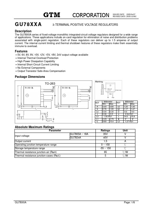
GU78XXA
Page: 2/6
元器件交易网
ISSUED DATE :2005/04/07 REVISED DATE :2005/12/06C
GU7808A (Refer to the test circuits, Tj=0~125к, Io=500mA, Vin=14V, Cin=0.33 F, Co=0.1 F unless otherwise specified)
VO (Load Regulation)
IQ
IQ
Vn RR VD Isc Ipk Vo / Tj
Min.
5.82 5.70
59 -
Typ.
6.0 5
1.5 14 4 4.3 45 2.0 550 2.2 -0.8
Max.
6.18 6.30 120 60 120 60 8.0 0.5 1.3
iso7810标准
iso7810标准ISO 7810标准ISO 7810标准是关于实体卡片的物理特性与尺寸的国际标准。
它规定了银行卡、身份证、驾驶证等实体卡片的标准尺寸,以确保这些卡片在尺寸上的一致性与兼容性。
本文将对ISO 7810标准的背景、内容和重要性进行介绍。
一、背景实体卡片的使用广泛应用于金融、交通、身份验证等领域。
为了确保这些实体卡片的互通性和适用性,国际标准化组织(ISO)制定了ISO 7810标准。
该标准最初于1985年发布,经过多年的修订和更新,目前已经成为实体卡片行业的公认标准。
二、内容ISO 7810标准主要包括以下几个方面的内容:1. 尺寸标准:ISO 7810标准规定了实体卡片的四个尺寸。
根据应用不同,实体卡片可以被分为四个尺寸,即ID-1、ID-2、ID-3和ID-000。
- ID-1尺寸是最常见的标准尺寸,也是银行卡、信用卡、驾驶证和身份证等常见卡片所采用的尺寸。
其尺寸为85.60mm × 53.98mm。
- ID-2尺寸相对较大,通常用于磁卡和身份证,尺寸为105mm ×74mm。
- ID-3尺寸通常用于护照,尺寸为125mm × 88mm。
- ID-000尺寸是最小的尺寸,通常用于芯片卡和SIM卡,尺寸为25mm × 15mm。
2. 材料要求:ISO 7810标准还规定了实体卡片所采用的材料要求。
根据标准要求,实体卡片必须采用耐久、抗静电、易塑性和易印刷的材料制成,以确保卡片的质量和可靠性。
3. 弯曲性测试:ISO 7810标准还包括对实体卡片的弯曲性能测试要求。
该测试旨在确保实体卡片在正常使用过程中具有足够的柔韧性和耐久性,以避免卡片在弯曲或弯曲后的损坏。
4. 兼容性:ISO 7810标准要求实体卡片在尺寸和材料方面的兼容性,确保不同制造商生产的卡片能够在各种设备和系统中互相兼容和使用。
这种兼容性是保障用户方便使用和系统正常运作的重要保证。
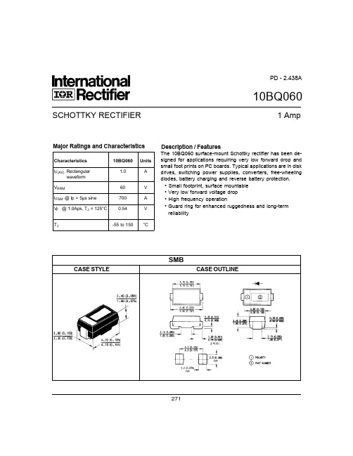
10BQ060中文资料
Characteristics
273
元器件交易网
10BQ060
155 150 145 140
DC
1.0 10BQ060 R thJC (DC) = 36°C/W
D = 0.08 D = 0.17 D = 0.25 0.8 D = 0.33 D = 0.50 0.6 DC 0.4
10BQ060
60
Absolute Maximum Ratings
Parameters
IF(AV) IFSM EAS IAR Max. Average Forward Current See Fig. 5 Max. Peak One Cycle Non - Repetitive Surge Current — see Fig. 7 Non - Repetitive Avalanche Energy Repetitive Avalanche Current 700 42 11 1.0 mJ A A 5µs Sine or 3µs Rect. pulse 10ms Sine 0r 6ms Rect. pulse Following any rated load condition and with rated VRRM applied.
Conditions
LM7810中文资料

UTC LM78XXLINEAR INTEGRATED CIRCUITUTC UNISONIC TECHNOLOGIES CO., LTD.1QW-R101-006,C3-TERMINAL 1A POSITIVE VOLTAGE REGULATORDESCRIPTIONThe UTC 78XX family is monolithic fixed voltageregulator integrated circuit. They are suitable for applications that required supply current up to 1 A.FEATURES*Output current up to 1.5 A*Fixed output voltage of 5V, 6V, 8V, 9V, 10V, 12V, 15V ,18V and 24V available*Thermal overload shutdown protection *Short circuit current limiting*Output transistor SOA protection1: Input 2: GND 3: OutputTEST CIRCUITINPUTZ1UTC LM78XXLINEAR INTEGRATED CIRCUITUTC UNISONIC TECHNOLOGIES CO., LTD.2QW-R101-006,CABSOLUTE MAXIMUM RATINGS( Operating temperature range applies unless otherwise specified )PARAMETER SYMBOL RATING UNITInput voltage(for Vo=5~18V)(for Vo=24V) V I 35 40V V Output CurrentI o 1 A Power DissipationPD Internally Limited W Operating Junction Temperature RangeT OPR-20+150°CStorage Temperature Range T STG -55+150 °C UTC LM7805 ELECTRICAL CHARACTERISTICS( VI=10V, Io=0.5A, Tj= 0°C - 125°C, C1=0.33uF, Co=0.1uF, unless otherwise specified )(Note 1)PARAMETERSYMBOLTEST CONDITIONSMINTYP MAX UNITTj=25°C, I O =5mA - 1.0A4.805.0 5.20 VOutput Voltage VoV I =7.5V to 20V, I O =5mA - 1.0A,PD<15W4.755.25 V Load Regulation∆Vo Tj =25°C,I O =5mA - 1.5A 50 mVTj=25°C,I O =0.25A - 0.75A 25 mVLine regulation ∆Vo V I =7V to 25V,Tj=25°C 50 mVV I =7.5V to 20V,Tj=25°C,Io=1A 50 mV Quiescent Current Iq Tj=25°C, I O =<1A 8.0 mAQuiescent Current Change ∆Iq V I =7.5V to 20V 1.0 mA∆Iq I O =5mA - 1.0A 0.5 mA Output Noise Voltage V N 10Hz<=f<=100kHz 40 µV Temperature coefficient of Vo ∆Vo/∆T Io =5mA -0.6mV/°C Ripple Rejection RR V I =8V - 18V,f=120Hz,Tj=25°C 6280 dB Peak Output Current I PK Tj=25°C 1.8 A Short-Circuit Current I SC VI=35V, Tj=25°C 250 mA Dropout Voltage Vd Tj=25°C 2.0 VUTC LM7806 ELECTRICAL CHARACTERISTICS( VI=11V, Io=0.5A, Tj= 0°C - 125°C, C1=0.33uF, Co=0.1uF, unless otherwise specified )(Note 1)PARAMETERSYMBOLTEST CONDITIONSMINTYP MAX UNITTj=25°C, I O =5mA - 1.0A5.766.0 6.24 V Output VoltageVoV I =8.5V to 21V,I O =5mA - 1.0A, PD<15W5.706.30 VLoad Regulation∆Vo Tj =25°C,I O =5mA - 1.5A 60 mVTj=25°C,I O =0.25A - 0.75A 30 mVLine regulation ∆Vo V I =8V to 25V,Tj=25°C 60 mVV I =8.5V to 21V,Tj=25°C,Io=1A 60 mV Quiescent Current Iq Tj=25°C, I O =<1A 8.0 mAQuiescent Current Change ∆Iq V I =8.5V to 21V 1.0 mA∆Iq I O =5mA - 1.0A 0.5 mA Output Noise Voltage V N 10Hz<=f<=100kHz 45 µV Temperature coefficient of Vo ∆Vo/∆T Io =5mA -0.7mV/°C Ripple RejectionRR V I =9V - 19V,f=120Hz,Tj=25°C 5975 dBUTC LM78XXLINEAR INTEGRATED CIRCUITUTC UNISONIC TECHNOLOGIES CO., LTD.3QW-R101-006,CPARAMETERSYMBOLTEST CONDITIONSMINTYP MAX UNITPeak Output Current I PK Tj=25°C 1.8 AShort-Circuit Current I SCVI=35V, Tj=25°C 250 mA Dropout Voltage VdTj=25°C 2.0 VUTC LM7808 ELECTRICAL CHARACTERISTICS( VI=14V, Io=0.5A, Tj= 0°C - 125°C, C1=0.33uF, Co=0.1uF, unless otherwise specified )(Note 1)PARAMETERSYMBOL TEST CONDITIONSMINTYP MAX UNITTj=25°C, I O =5mA - 1.0A 7.688.0 8.32 V Output VoltageVoV I =10.5V to 23V,I O =5mA - 1.0A, PD<15W7.608.40 VLoad Regulation ∆Vo Tj =25°C,I O =5mA - 1.5A 80 mVTj=25°C,I O =0.25A - 0.75A 40 mVLine regulation ∆Vo V I =10.5V to 25V,Tj=25°C 80 mVV I =10.5V to 23V,Tj=25°C,Io=1A 80 mV Quiescent Current Iq Tj=25°C, I O =<1A 8.0 mAQuiescent Current Change ∆Iq V I =10.5V to 23V 1.0 mA ∆Iq I O =5mA - 1.0A 0.5 mAOutput Noise Voltage V N 10Hz<=f<=100kHz 58 µVTemperature coefficient of Vo ∆Vo/∆T Io =5mA -0.9mV/°C Ripple Rejection RR V I =11.5V to 21.5V, f=120Hz,Tj=25°C 5672 dBPeak Output Current I PK Tj=25°C 1.8 A Short-Circuit Current I SC VI=35V, Tj=25°C 250 mA Dropout Voltage Vd Tj=25°C 2.0 VUTC LM7809 ELECTRICAL CHARACTERISTICS( VI=15V, Io=0.5A, Tj= 0°C - 125°C, C1=0.33uF, Co=0.1uF, unless otherwise specified )(Note 1)PARAMETERSYMBOLTEST CONDITIONSMINTYP MAX UNITTj=25°C, I O =5mA - 1.0A8.649.0 9.36 VOutput Voltage VoV I =11.5V to 24V, I O =5mA - 1.0A,PD<15W8.55 9.45 V Load Regulation ∆Vo Tj =25°C,I O =5mA - 1.5A 90 mVTj=25°C,I O =0.25A - 0.75A 45 mVLine regulation ∆Vo V I =11.5V to 25 V, Tj=25°C, PD<15W90 mVV I =11.5V to 24V,Tj=25°C, Io<=1A90 mV Quiescent Current Iq Tj=25°C, I O =<1A 8.0 mAQuiescent Current Change ∆Iq V I =11.5V to 24V 1.0 mA∆Iq I O =5mA – 1.0A 0.5 mA Output Noise Voltage V N 10Hz<=f<=100kHz 58 µV Temperature coefficient of Vo ∆Vo/∆T Io =5mA -1.1 mV/°C Ripple Rejection RR V I =12.5V to 22.5V, f=120Hz,Tj=25°C 5672 dBPeak Output Current I PK Tj=25°C 1.8 A Short-Circuit Current I SC VI=35V, Tj=25°C 250 mA Dropout Voltage Vd Tj=25°C 2.0 VUTC LM78XXLINEAR INTEGRATED CIRCUITUTC UNISONIC TECHNOLOGIES CO., LTD.4QW-R101-006,CUTC LM7810 ELECTRICAL CHARACTERISTICS( VI=16V, Io=0.5A, Tj= 0°C - 125°C, C1=0.33uF, Co=0.1uF, unless otherwise specified )(Note 1) PARAMETERSYMBOLTEST CONDITIONSMINTYP MAX UNITTj=25°C, I O =5mA - 1.0A9.6010.0 10.40 V Output Voltage Vo VI =12.5V to 25V,I O =5mA - 1.0A,PD<=15W9.5010.50 VLoad Regulation ∆Vo Tj =25°C,I O =5mA - 1.5A 100 mVTj=25°C,I O =0.25A - 0.75A 50 mVLine regulation ∆Vo VI =13V to 25V,Tj=25°C 100 mVVI =13V to 25V, Tj=25°C,Io<=1A 100 mVQuiescent Current Iq Tj=25°C, I O =<1A 8.0 mAQuiescent Current Change ∆Iq VI =12.6V to 25V 1.0 mA ∆Iq I O =5mA - 1.0A 0.5 mAOutput Noise Voltage V N 10Hz<=f<=100kHz 58 µVTemperature coefficient of Vo ∆Vo/∆T Io =5mA -1.1mV/°C Ripple Rejection RR VI =13V - 23V,f=120Hz,Tj=25°C 5672 dBPeak Output Current I PK Tj=25°C 1.8 A Short-Circuit Current I SC VI=35V, Tj=25°C 250 mA Dropout Voltage Vd Tj=25°C 2.0 VUTC LM7812 ELECTRICAL CHARACTERISTICS( VI=19V, Io=0.5A, Tj= 0°C - 125°C, C1=0.33uF, Co=0.1uF, unless otherwise specified )(Note 1)PARAMETER SYMBOLTEST CONDITIONS MIN TYP MAX UNITTj=25°C, I O =5mA - 1.0A 11.5212.0 12.48 VOutput Voltage VoV I =14.5V to 27V,I O =5mA - 1.0A,PD<15W11.40 12.60 V Load Regulation∆Vo Tj =25°C,I O =5mA - 1.5A 120 mVTj=25°C,I O =0.25A - 0.75A 60 mVLine regulation ∆Vo V I =14.5V to 30V,Tj=25°C 120 mVV I =14.6V to 27V,Tj=25°C, Io=1A120 mV Quiescent Current Iq Tj=25°C, I O =<1A 8.0 mAQuiescent Current Change ∆Iq V I =14.5V to 30V 1.0 mA∆Iq I O =5mA - 1.0A 0.5 mA Output Noise Voltage V N 10Hz<=f<=100kHz 75 µV Temperature coefficient of Vo ∆Vo/∆T Io =5mA -1.5mV/°C Ripple Rejection RR V I =15V - 25V,f=120Hz,Tj=25°C 5572 dB Peak Output Current I PK Tj=25°C 1.8 A Short-Circuit Current I SC VI=35V, Tj=25°C 250 mA Dropout Voltage Vd Tj=25°C 2.0 VUTC LM78XXLINEAR INTEGRATED CIRCUITUTC UNISONIC TECHNOLOGIES CO., LTD.5QW-R101-006,CUTC LM7815 ELECTRICAL CHARACTERISTICS( VI=23V, Io=0.5A, Tj= 0°C - 125°C, C1=0.33uF, Co=0.1uF, unless otherwise specified )(Note 1)PARAMETERSYMBOLTEST CONDITIONSMINTYP MAX UNITTj=25°C, I O =5mA - 1.0A14.4015.0 15.60 V Output VoltageVoV I =17.5V to 30V,I O =5mA - 1.0A,PD<15W 14.2515.75 VLoad Regulation ∆Vo Tj =25°C,I O =5mA - 1.5A 150 mVTj=25°C,I O =0.25A - 0.75A 75 mVLine regulation ∆Vo V I =18.5V to 30V,Tj=25°C 150 mVV I =17.7V to 30V, Tj=25°C, I O =1A 150 mV Quiescent Current Iq Tj=25°C, I O =<1A 8.0 mAQuiescent Current Change ∆Iq V I =17.5V to 30V 1.0 mA ∆Iq I O =5mA - 1.0A 0.5 mAOutput Noise Voltage V N 10Hz<=f<=100kHz 90 µVTemperature coefficient of Vo ∆Vo/∆T Io =5mA -1.8mV/°C Ripple Rejection RR V I =18.5V to 28.5V f=120Hz,Tj=25°C5470 dBPeak Output Current I PK Tj=25°C 1.8 A Short-Circuit Current I SC VI=35V, Tj=25°C 250 mA Dropout Voltage Vd Tj=25°C 2.0 VUTC LM7818 ELECTRICAL CHARACTERISTICS( VI=27V, Io=0.5A, Tj= 0°C - 125°C, C1=0.33uF, Co=0.1uF, unless otherwise specified )(Note 1)PARAMETERSYMBOLTEST CONDITIONSMINTYP MAX UNITTj=25°C, I O =5mA - 1.0A17.2818.0 18.72 VOutput Voltage VoV I =21V to 33V,I O =5mA - 1.0A 17.1018.90 V Load Regulation∆Vo Tj =25°C,I O =5mA - 1.5A 180 mVTj=25°C,I O =0.25A - 0.75A 90 mVLine regulation ∆Vo V I =21V to 33V,Tj=25°C 180 mVV I =21V to 33V,Tj=25°C, I O =<1A,PD<15W 180 mV Quiescent Current Iq Tj=25°C, I O =<1A 8.0 mAQuiescent Current Change ∆Iq V I =21.5V to 33V 1.0 mA∆Iq I O =5mA - 1.0A 0.5 mA Output Noise Voltage V N 10Hz<=f<=100kHz 110 µV Temperature coefficient of Vo ∆Vo/∆T Io =5mA -2.2mV/°C Ripple Rejection RR V I =22V - 32V,f=120Hz,Tj=25°C 5369 dB Peak Output Current I PK Tj=25°C 1.8 A Short-Circuit Current I SC VI=35V, Tj=25°C 250 mA Dropout Voltage Vd Tj=25°C 2.0 VUTC LM78XXLINEAR INTEGRATED CIRCUITUTC UNISONIC TECHNOLOGIES CO., LTD.6QW-R101-006,CUTC LM7824 ELECTRICAL CHARACTERISTICS( VI=33V, Io=0.5A, Tj= 0°C - 12°C, C1=0.33uF, Co=0.1uF, unless otherwise specified )(Note 1)PARAMETERSYMBOLTEST CONDITIONSMINTYP MAX UNITTj=25°C, I O =5mA - 1.0A23.0424.0 24.96 VOutput VoltageVoV I =27V to 38V,I O =5mA - 1.0A 22.8025.20 V Load Regulation ∆Vo Tj =25°C,I O =5mA - 1.5A 240 mVTj=25°C,I O =0.25A - 0.75A 120 mVLine regulation ∆Vo V I =27V to 38V,Tj=25°C 240 mVV I =27V to 38V,Tj=25°C,Io=1A 240 mV Quiescent Current Iq Tj=25°C, I O =<1A 8.0 mAQuiescent Current Change ∆Iq V I =28V to 38V 1.0 mA ∆Iq I O =5mA - 1.0A 0.5 mAOutput Noise Voltage V N 10Hz<=f<=100kHz 170 µVTemperature coefficient of Vo ∆Vo/∆T Io =5mA -2.8mV/°C Ripple Rejection RR V I =28V - 38V,f=120Hz,Tj=25°C 5066 dB Peak Output Current I PK Tj=25°C 1.8 A Short-Circuit Current I SC VI=35V, Tj=25°C 250 mA Dropout Voltage Vd Tj=25°C 2.0 VNote 1: The Maximum steady state usable output current are dependent on input voltage, heat sinking, lead lengthof the package and copper pattern of PCB. The data above represents pulse test conditions with junction temperatures specified at the initiation of test.Note 2: Power dissipation<0.5WAPPLICATION CIRCUITNote 1: To specify an output voltage, substitute voltage value for "XX".Note 2: Bypass capacitors are recommended for optimum stability and transient response and should be located asclose as possible to the regulators.。
KA7810中文资料
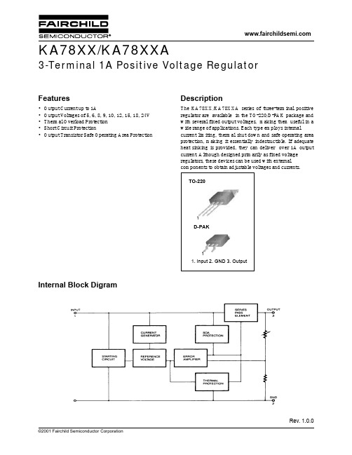
Rev. 1.0.0Features•Output Current up to 1A •Output V oltages of 5, 6, 8, 9, 10, 12, 15, 18, 24V•Thermal Overload Protection •Short Circuit Protection•Output Transistor Safe Operating Area ProtectionDescriptionThe KA78XX/KA78XXA series of three-terminal positive regulator are available in the TO-220/D-PAK package and with several fixed output voltages, making them useful in a wide range of applications. Each type employs internalcurrent limiting, thermal shut down and safe operating area protection, making it essentially indestructible. If adequate heat sinking is provided, they can deliver over 1A output current. Although designed primarily as fixed voltage regulators, these devices can be used with external components to obtain adjustable voltages and currents.TO-220D-PAK1. Input2. GND3. Output11Internal Block DigramKA78XX/KA78XXA3-Terminal 1A Positive Voltage RegulatorKA78XX/KA78XXAAbsolute Maximum RatingsElectrical Characteristics (KA7805/KA7805R)(Refer to test circuit ,0°C < T J < 125°C, I O = 500mA, V I =10V, C I = 0.33µF, C O =0.1µF, unless otherwise specified)Note:1. Load and line regulation are specified at constant junction temperature. Changes in V o due to heating effects must be takeninto account separately. Pulse testing with low duty is used.ParameterSymbol Value Unit Input Voltage (for V O = 5V to 18V)(for V O = 24V)V I V I 3540V V Thermal Resistance Junction-Cases (TO-220)R θJC 5°C/WThermal Resistance Junction-Air (TO-220)R θJA 65°C/WOperating Temperature Range (KA78XX/A/R)T OPR 0 ~ +125°C Storage Temperature RangeT STG-65 ~ +150°CParameterSymbolConditionsKA7805UnitMin.Typ.Max.Output VoltageV OT J =+25 o C4.85.0 5.25.0mA ≤Io ≤1.0A, P O ≤15W V I = 7V to 20V 4.75 5.0 5.25 V Line Regulation (Note1)Regline T J =+25 o C V O = 7V to 25V - 4.0100mV V I = 8V to 12V - 1.650Load Regulation (Note1)Regload T J =+25 o C I O = 5.0mA to1.5A -9100mV I O =250mA to 750mA -450Quiescent Current I Q T J =+25 o C - 5.08.0mA Quiescent Current Change ∆I Q I O = 5mA to 1.0A -0.030.5mA V I = 7V to 25V -0.3 1.3Output Voltage Drift ∆V O /∆T I O = 5mA--0.8-mV/ o C Output Noise Voltage V N f = 10Hz to 100KHz, T A =+25 o C -42-µV/V O Ripple Rejection RR f = 120HzV O = 8V to 18V 6273-dB Dropout Voltage V Drop I O = 1A, T J =+25 o C -2-V Output Resistance r O f = 1KHz-15-m ΩShort Circuit Current I SC V I = 35V, T A =+25 o C -230-mA Peak CurrentI PKT J =+25 o C- 2.2-AKA78XX/KA78XXAElectrical Characteristics (KA7806/KA7806R)(Refer to test circuit ,0°C < T J < 125°C, I O = 500mA, V I =11V, C I = 0.33µF, C O =0.1µF, unless otherwise specified)Note:1. Load and line regulation are specified at constant junction temperature. Changes in V O due to heating effects must be takeninto account separately. Pulse testing with low duty is used.ParameterSymbolConditionsKA7806UnitMin.Typ.Max.Output VoltageV OT J =+25 o C5.756.0 6.255.0mA ≤I O ≤1.0A, P O ≤15W V I = 8.0V to 21V 5.7 6.0 6.3 V Line Regulation (Note1)Regline T J =+25 o C V I = 8V to 25V -5120mV V I = 9V to 13V - 1.560Load Regulation (Note1)Regload T J =+25 o C I O =5mA to 1.5A -9120mV I O =250mA to750mA -360Quiescent Current I Q T J =+25 o C - 5.08.0mA Quiescent Current Change ∆I Q I O = 5mA to 1A --0.5mA V I = 8V to 25V -- 1.3Output Voltage Drift ∆V O /∆T I O = 5mA--0.8-mV/ o C Output Noise Voltage V N f = 10Hz to 100KHz, T A =+25 o C -45-µV/Vo Ripple Rejection RR f = 120HzV I = 9V to 19V 5975-dB Dropout Voltage V Drop I O = 1A, T J =+25 o C -2-V Output Resistance r O f = 1KHz-19-m ΩShort Circuit Current I SC V I = 35V, T A =+25 o C -250-mA Peak CurrentI PKT J =+25 o C- 2.2-AKA78XX/KA78XXAElectrical Characteristics (KA7808/KA7808R)(Refer to test circuit ,0°C < T J < 125°C, I O = 500mA, V I =14V, C I = 0.33µF, C O =0.1µF, unless otherwise specified)Note:1. Load and line regulation are specified at constant junction temperature. Changes in V O due to heating effects must be takeninto account separately. Pulse testing with low duty is used.ParameterSymbolConditionsKA7808UnitMin.Typ.Max.Output VoltageV OT J =+25 o C7.78.08.35.0mA ≤ I O ≤1.0A, P O ≤15W V I = 10.5V to 23V 7.68.08.4 V Line Regulation (Note1)ReglineT J =+25 o C V I = 10.5V to 25V - 5.0160mV V I = 11.5V to 17V - 2.080Load Regulation (Note1)Regload T J =+25 o C I O = 5.0mA to 1.5A-10160mV I O = 250mA to 750mA - 5.080Quiescent Current I Q T J =+25 o C - 5.08.0mA Quiescent Current Change ∆I Q I O = 5mA to 1.0A -0.050.5mA V I = 10.5A to 25V -0.5 1.0Output Voltage Drift ∆V O /∆T I O = 5mA--0.8-mV/ o C Output Noise Voltage V N f = 10Hz to 100KHz, T A =+25 o C -52-µV/Vo Ripple Rejection RR f = 120Hz, V I = 11.5V to 21.5V 5673-dB Dropout Voltage V Drop I O = 1A, T J =+25 o C -2-V Output Resistance r O f = 1KHz-17-m ΩShort Circuit Current I SC V I = 35V, T A =+25 o C -230-mA Peak CurrentI PKT J =+25 o C- 2.2-AKA78XX/KA78XXAElectrical Characteristics (KA7809/KA7809R)(Refer to test circuit ,0°C < T J < 125°C, I O = 500mA, V I =15V, C I = 0.33µF, C O =0.1µF, unless otherwise specified)Note:1. Load and line regulation are specified at constant junction temperature. Changes in V O due to heating effects must be takeninto account separately. Pulse testing with low duty is used.ParameterSymbolConditionsKA7809UnitMin.Typ.Max.Output VoltageV OT J =+25 o C8.6599.355.0mA ≤ I O ≤1.0A, P O ≤15W V I = 11.5V to 24V 8.699.4 V Line Regulation (Note1)Regline T J =+25 o C V I = 11.5V to 25V -6180mV V I = 12V to 17V -290Load Regulation (Note1)Regload T J =+25 o C I O = 5mA to 1.5A -12180mV I O = 250mA to 750mA -490Quiescent Current I Q T J =+25 o C - 5.08.0mA Quiescent Current Change ∆I Q I O = 5mA to 1.0A --0.5mA V I = 11.5V to 26V -- 1.3Output Voltage Drift ∆V O /∆T I O = 5mA--1-mV/ o C Output Noise Voltage V N f = 10Hz to 100KHz, T A =+25 o C -58-µV/Vo Ripple Rejection RR f = 120HzV I = 13V to 23V 5671-dB Dropout Voltage V Drop I O = 1A, T J =+25 o C -2-V Output Resistance r O f = 1KHz-17-m ΩShort Circuit Current I SC V I = 35V, T A =+25 o C -250-mA Peak CurrentI PKT J = +25 o C- 2.2-AElectrical Characteristics (KA7810)(Refer to test circuit ,0°C < T J < 125°C, I O = 500mA, V I =16V, C I = 0.33µF, C O =0.1µF, unless otherwise specified)Note:1. Load and line regulation are specified at constant junction temperature. Changes in V O due to heating effects must be takeninto account separately. Pulse testing with low duty is used.ParameterSymbolConditionsKA7810UnitMin.Typ.Max.Output VoltageV OT J =+25 o C9.61010.45.0mA ≤ I O ≤ 1.0A, P O ≤ 15W V I = 12.5V to 25V 9.51010.5 V Line Regulation (Note1)Regline T J =+25 o C V I = 12.5V to 25V -10200mV V I = 13V to 25V -3100Load Regulation (Note1)Regload T J =+25 o C I O = 5mA to 1.5A -12200mV I O = 250mA to 750mA -4400Quiescent Current I Q T J =+25 o C - 5.18.0mA Quiescent Current Change ∆I Q I O = 5mA to 1.0A --0.5mA V I = 12.5V to 29V -- 1.0Output Voltage Drift ∆V O /∆T I O = 5mA--1-mV/ o C Output Noise Voltage V N f = 10Hz to 100KHz, T A =+25 o C -58-µV/Vo Ripple Rejection RR f = 120HzV I = 13V to 23V 5671-dB Dropout Voltage V Drop I O = 1A, T J =+25 o C -2-V Output Resistance r O f = 1KHz-17-m ΩShort Circuit Current I SC V I = 35V, T A =+25 o C -250-mA Peak CurrentI PKT J =+25 o C- 2.2-AElectrical Characteristics (KA7812/KA7812R)(Refer to test circuit ,0°C < T J < 125°C, I O = 500mA, V I =19V, C I = 0.33µF, C O =0.1µF, unless otherwise specified)Note:1. Load and line regulation are specified at constant junction temperature. Changes in V O due to heating effects must be takeninto account separately. Pulse testing with low duty is used.ParameterSymbolConditionsKA7812/KA7812R UnitMin.Typ.Max.Output VoltageV OT J =+25 o C11.51212.55.0mA ≤ I O ≤1.0A, P O ≤15W V I = 14.5V to 27V 11.41212.6 V Line Regulation (Note1)ReglineT J =+25 o CV I = 14.5V to 30V -10240mV V I = 16V to 22V - 3.0120Load Regulation (Note1)Regload T J =+25 o C I O = 5mA to 1.5A -11240mV I O = 250mA to 750mA - 5.0120Quiescent Current I Q T J =+25 o C - 5.18.0mA Quiescent Current Change ∆I Q I O = 5mA to 1.0A -0.10.5mA V I = 14.5V to 30V -0.5 1.0Output Voltage Drift ∆V O /∆T I O = 5mA--1-mV/ o C Output Noise Voltage V N f = 10Hz to 100KHz, T A =+25 o C -76-µV/Vo Ripple Rejection RR f = 120HzV I = 15V to 25V 5571-dB Dropout Voltage V Drop I O = 1A, T J =+25 o C -2-V Output Resistance r O f = 1KHz-18-m ΩShort Circuit Current I SC V I = 35V, T A =+25 o C -230-mA Peak CurrentI PKT J = +25 o C- 2.2-AKA78XX/KA78XXAElectrical Characteristics (KA7815)(Refer to test circuit ,0°C < T J < 125°C, I O = 500mA, V I =23V, C I = 0.33µF, C O =0.1µF, unless otherwise specified)Note:1. Load and line regulation are specified at constant junction temperature. Changes in V O due to heating effects must be takeninto account separately. Pulse testing with low duty is used.ParameterSymbolConditionsKA7815UnitMin.Typ.Max.Output VoltageV OT J =+25 o C14.41515.65.0mA ≤ I O ≤1.0A, P O ≤15W V I = 17.5V to 30V 14.251515.75 V Line Regulation (Note1)Regline T J =+25 o C V I = 17.5V to 30V -11300mV V I = 20V to 26V -3150Load Regulation (Note1)Regload T J =+25 o C I O = 5mA to 1.5A -12300mV I O = 250mA to 750mA -4150Quiescent Current I Q T J =+25 o C - 5.28.0mA Quiescent Current Change ∆I Q I O = 5mA to 1.0A --0.5mA V I = 17.5V to 30V -- 1.0Output Voltage Drift ∆V O /∆T I O = 5mA--1-mV/ o C Output Noise Voltage V N f = 10Hz to 100KHz, T A =+25 o C -90-µV/Vo Ripple Rejection RR f = 120HzV I = 18.5V to 28.5V 5470-dB Dropout Voltage V Drop I O = 1A, T J =+25 o C -2-V Output Resistance r O f = 1KHz-19-m ΩShort Circuit Current I SC V I = 35V, T A =+25 o C -250-mA Peak CurrentI PKT J =+25 o C- 2.2-AKA78XX/KA78XXAElectrical Characteristics (KA7818)(Refer to test circuit ,0°C < T J < 125°C, I O = 500mA, V I =27V, C I = 0.33µF, C O =0.1µF, unless otherwise specified)Note:1. Load and line regulation are specified at constant junction temperature. Changes in V O due to heating effects must be takeninto account separately. Pulse testing with low duty is used.ParameterSymbolConditionsKA7818UnitMin.Typ.Max.Output VoltageV OT J =+25 o C17.31818.75.0mA ≤ I O ≤1.0A, P O ≤15W V I = 21V to 33V 17.11818.9 V Line Regulation (Note1)Regline T J =+25 o C V I = 21V to 33V -15360mV V I = 24V to 30V -5180Load Regulation (Note1)Regload T J =+25 o C I O = 5mA to 1.5A -15360mV I O = 250mA to 750mA - 5.0180Quiescent Current I Q T J =+25 o C - 5.28.0mA Quiescent Current Change ∆I Q I O = 5mA to 1.0A --0.5mA V I = 21V to 33V --1Output Voltage Drift ∆V O /∆T I O = 5mA--1-mV/ o C Output Noise Voltage V N f = 10Hz to 100KHz, T A =+25 o C -110-µV/Vo Ripple Rejection RR f = 120HzV I = 22V to 32V 5369-dB Dropout Voltage V Drop I O = 1A, T J =+25 o C -2-V Output Resistance r O f = 1KHz-22-m ΩShort Circuit Current I SC V I = 35V, T A =+25 o C -250-mA Peak CurrentI PKT J =+25 o C-2.2-AKA78XX/KA78XXAElectrical Characteristics (KA7824)(Refer to test circuit ,0°C < T J < 125°C, I O = 500mA, V I =33V, C I = 0.33µF, C O =0.1µF, unless otherwise specified)Note:1. Load and line regulation are specified at constant junction temperature. Changes in V O due to heating effects must be takeninto account separately. Pulse testing with low duty is used.ParameterSymbolConditionsKA7824UnitMin.Typ.Max.Output VoltageV OT J =+25 o C2324255.0mA ≤ I O ≤ 1.0A, P O ≤ 15W V I = 27V to 38V 22.82425.25 V Line Regulation (Note1)ReglineT J =+25 o CV I = 27V to 38V -17480mV V I = 30V to 36V -6240Load Regulation (Note1)Regload T J =+25 o C I O = 5mA to 1.5A -15480mV I O = 250mA to 750mA - 5.0240Quiescent Current I Q T J =+25 o C - 5.28.0mA Quiescent Current Change ∆I QI O = 5mA to 1.0A -0.10.5mA V I = 27V to 38V-0.51Output Voltage Drift ∆V O /∆T I O = 5mA --1.5-mV/ o C Output Noise Voltage V N f = 10Hz to 100KHz, T A =+25 o C -60-µV/Vo Ripple Rejection RR f = 120HzV I = 28V to 38V 5067-dB Dropout Voltage V Drop I O = 1A, T J =+25 o C -2-V Output Resistance r O f = 1KHz-28-m ΩShort Circuit Current I SC V I = 35V, T A =+25 o C -230-mA Peak CurrentI PKT J =+25 o C- 2.2-AKA78XX/KA78XXAElectrical Characteristics (KA7805A)(Refer to the test circuits. 0o C < T J < +125 o C, I o =1A, V I = 10V, C I =0.33µF, C O =0.1µF, unless otherwise speci-fied)Note:1. Load and line regulation are specified at constant junction temperature. Change in V O due to heating effects must be takeninto account separately. Pulse testing with low duty is used.ParameterSymbol ConditionsMin.Typ.Max.UnitOutput VoltageV OT J =+25 o C4.955.1V I O = 5mA to 1A, P O ≤ 15W V I = 7.5V to 20V 4.85 5.2Line Regulation (Note1)ReglineV I = 7.5V to 25V I O = 500mA-550mV V I = 8V to 12V -350T J =+25 o CV I = 7.3V to 20V -550V I = 8V to 12V- 1.525Load Regulation (Note1)RegloadT J =+25 o CI O = 5mA to 1.5A -9100mV I O = 5mA to 1A -9100I O = 250mA to 750mA -450Quiescent Current I Q T J =+25 o C - 5.0 6.0mA Quiescent Current Change∆I Q I O = 5mA to 1A--0.5mA V I = 8 V to 25V, I O = 500mA --0.8V I = 7.5V to 20V, T J =+25 o C --0.8Output Voltage Drift ∆V/∆T Io = 5mA--0.8-mV/ o C Output Noise Voltage V N f = 10Hz to 100KHz T A =+25 o C-10-µV/Vo Ripple Rejection RR f = 120Hz, I O = 500mA V I = 8V to 18V -68-dB Dropout Voltage V Drop I O = 1A, T J =+25 o C -2-V Output Resistance r O f = 1KHz-17-m ΩShort Circuit Current I SC V I = 35V, T A =+25 o C -250-mA Peak CurrentI PKT J = +25 o C- 2.2-AKA78XX/KA78XXAElectrical Characteristics (KA7806A)(Refer to the test circuits. 0o C < T J < +125 o C, I o =1A, V I = 11V, C I =0.33µF, C O =0.1µF, unless otherwise speci-fied)Note:1. Load and line regulation are specified at constant junction temperature. Change in V O due to heating effects must be takeninto account separately. Pulse testing with low duty is used.ParameterSymbol ConditionsMin.Typ.Max.UnitOutput VoltageV OT J =+25 o C5.5866.12V I O = 5mA to 1A, P O ≤ 15W V I = 8.6V to 21V 5.766 6.24Line Regulation (Note1)ReglineV I = 8.6V to 25V I O = 500mA-560mV V I = 9V to 13V -360T J =+25 o CV I = 8.3V to 21V -560V I = 9V to 13V- 1.530Load Regulation (Note1)RegloadT J =+25 o CI O = 5mA to 1.5A -9100mV I O = 5mA to 1A -4100I O = 250mA to 750mA - 5.050Quiescent Current I Q T J =+25 o C - 4.3 6.0mA Quiescent Current Change ∆I Q I O = 5mA to 1A--0.5mA V I = 9V to 25V, I O = 500mA --0.8V I = 8.5V to 21V, T J =+25 o C --0.8Output Voltage Drift ∆V/∆T I O = 5mA--0.8-mV/ o C Output Noise Voltage V N f = 10Hz to 100KHz T A =+25 o C-10-µV/Vo Ripple Rejection RR f = 120Hz, I O = 500mA V I = 9V to 19V -65-dB Dropout Voltage V Drop I O = 1A, T J =+25 o C -2-V Output Resistance r O f = 1KHz-17-m ΩShort Circuit Current I SC V I = 35V, T A =+25 o C -250-mA Peak CurrentI PKT J =+25 o C- 2.2-AKA78XX/KA78XXAElectrical Characteristics (KA7808A)(Refer to the test circuits. 0o C < T J < +125 o C, I o =1A, V I = 14V, C I =0.33µF, C O =0.1µF, unless otherwise speci-fied)Note:1. Load and line regulation are specified at constant junction temperature. Change in V O due to heating effects must be takeninto account separately. Pulse testing with low duty is used.ParameterSymbol ConditionsMin.Typ.Max.UnitOutput VoltageV OT J =+25 o C7.8488.16V I O = 5mA to 1A, P O ≤15W V I = 10.6V to 23V 7.788.3Line Regulation (Note1)ReglineV I = 10.6V to 25V I O = 500mA-680mV V I = 11V to 17V -380T J =+25 o CV I = 10.4V to 23V -680V I = 11V to 17V-240Load Regulation (Note1)RegloadT J =+25 o CI O = 5mA to 1.5A -12100mV I O = 5mA to 1A -12100I O = 250mA to 750mA -550Quiescent Current I Q T J =+25 o C - 5.0 6.0mA Quiescent Current Change ∆I Q I O = 5mA to 1A--0.5mA V I = 11V to 25V, I O = 500mA --0.8V I = 10.6V to 23V, T J =+25 o C --0.8Output Voltage Drift ∆V/∆T I O = 5mA--0.8-mV/ o C Output Noise Voltage V N f = 10Hz to 100KHz T A =+25 o C-10-µV/Vo Ripple Rejection RR f = 120Hz, I O = 500mA V I = 11.5V to 21.5V -62-dB Dropout Voltage V Drop I O = 1A, T J =+25 o C -2-V Output Resistance r O f = 1KHz-18-m ΩShort Circuit Current I SC V I = 35V, T A =+25 o C -250-mA Peak CurrentI PKT J =+25 o C- 2.2-AKA78XX/KA78XXAElectrical Characteristics (KA7809A)(Refer to the test circuits. 0o C < T J < +125 o C, I o =1A, V I = 15V, C I =0.33µF, C O =0.1µF, unless otherwise speci-fied)Note:1. Load and line regulation are specified at constant junction temperature. Change in V O due to heating effects must be takeninto account separately. Pulse testing with low duty is used.ParameterSymbolConditionsMin.Typ.Max.UnitOutput VoltageV OT J =+25°C8.829.09.18V I O = 5mA to 1A, P O ≤15W V I = 11.2V to 24V 8.659.09.35Line Regulation (Note1)ReglineV I = 11.7V to 25V I O = 500mA-690mV V I = 12.5V to 19V -445T J =+25°CV I = 11.5V to 24V -690 V I = 12.5V to 19V -245Load Regulation (Note1)RegloadT J =+25°CI O = 5mA to 1.0A -12100mV I O = 5mA to 1.0A -12100I O = 250mA to 750mA -550Quiescent Current I Q T J =+25 °C- 5.0 6.0mA Quiescent Current Change ∆I Q V I = 11.7V to 25V, T J =+25 °C --0.8mA V I = 12V to 25V, I O = 500mA --0.8I O = 5mA to 1.0A --0.5Output Voltage Drift ∆V/∆T I O = 5mA--1.0-mV/ °C Output Noise Voltage V N f = 10Hz to 100KHz T A =+25 °C-10-µV/Vo Ripple Rejection RR f = 120Hz, I O = 500mA V I = 12V to 22V -62-dB Dropout Voltage V Drop I O = 1A, T J =+25 °C - 2.0-V Output Resistance r O f = 1KHz-17-m ΩShort Circuit Current I SC V I = 35V, T A =+25 °C -250-mA Peak CurrentI PKT J =+25°C- 2.2-A(Refer to the test circuits. 0o C < T J < +125 o C, I o =1A, V I = 16V, C I =0.33µF, C O =0.1µF, unless otherwise speci-fied)Note:1. Load and line regulation are specified at constant junction temperature. Change in V O due to heating effects must be takeninto account separately. Pulse testing with low duty is used.ParameterSymbolConditionsMin.Typ.Max.UnitOutput VoltageV OT J =+25°C9.81010.2V I O = 5mA to 1A, P O ≤ 15W V I =12.8V to 25V 9.61010.4Line Regulation (Note1)ReglineV I = 12.8V to 26V I O = 500mA-8100mV V I = 13V to 20V -450 T J =+25 °CV I = 12.5V to 25V -8100 V I = 13V to 20V -350Load Regulation (Note1)RegloadT J =+25 °CI O = 5mA to 1.5A -12100mV I O = 5mA to 1.0A -12100 I O = 250mA to 750mA -550Quiescent Current I Q T J =+25 °C- 5.0 6.0mA Quiescent Current Change ∆I QV I = 13V to 26V, T J =+25 °C --0.5mA V I = 12.8V to 25V, I O = 500mA --0.8 I O = 5mA to 1.0A--0.5Output Voltage Drift ∆V/∆T I O = 5mA --1.0-mV/ °C Output Noise Voltage V N f = 10Hz to 100KHz T A =+25 °C-10-µV/Vo Ripple Rejection RR f = 120Hz, I O = 500mA V I = 14V to 24V -62-dB Dropout Voltage V Drop I O = 1A, T J =+25°C - 2.0-V Output Resistance r O f = 1KHz-17-m ΩShort Circuit Current I SC V I = 35V, T A =+25 °C -250-mA Peak CurrentI PKT J =+25 °C- 2.2-A(Refer to the test circuits. 0o C < T J < +125 o C, I o =1A, V I = 19V, C I =0.33µF, C O =0.1µF, unless otherwise speci-fied)Note:1. Load and line regulation are specified at constant junction temperature. Change in V O due to heating effects must be takeninto account separately. Pulse testing with low duty is used.ParameterSymbol ConditionsMin.Typ.Max.UnitOutput VoltageV OT J =+25 °C11.751212.25V I O = 5mA to 1A, P O ≤15W V I = 14.8V to 27V 11.51212.5Line Regulation (Note1)ReglineV I = 14.8V to 30V I O = 500mA-10120mV V I = 16V to 22V -4120 T J =+25 °CV I = 14.5V to 27V -10120 V I = 16V to 22V-360Load Regulation (Note1)RegloadT J =+25 °CI O = 5mA to 1.5A -12100mV I O = 5mA to 1.0A -12100 I O = 250mA to 750mA -550Quiescent Current I Q T J =+25°C- 5.16.0mA Quiescent Current Change ∆I QV I = 15V to 30V, T J =+25 °C -0.8mA V I = 14V to 27V, I O = 500mA -0.8 I O = 5mA to 1.0A-0.5Output Voltage Drift ∆V/∆T I O = 5mA --1.0-mV/°C Output Noise Voltage V N f = 10Hz to 100KHz T A =+25°C-10-µV/Vo Ripple Rejection RR f = 120Hz, I O = 500mA V I = 14V to 24V -60-dB Dropout Voltage V Drop I O = 1A, T J =+25°C - 2.0-V Output Resistance r O f = 1KHz-18-m ΩShort Circuit Current I SC V I = 35V, T A =+25 °C -250-mA Peak CurrentI PKT J =+25 °C- 2.2-AKA78XX/KA78XXAElectrical Characteristics (KA7815A)(Refer to the test circuits. 0o C < T J < +125 o C, I o =1A, V I =23V, C I =0.33µF, C O =0.1µF, unless otherwise speci-fied)Note:1. Load and line regulation are specified at constant junction temperature. Change in V O due to heating effects must be takeninto account separately. Pulse testing with low duty is used.ParameterSymbol ConditionsMin.Typ.Max.UnitOutput VoltageV OT J =+25 °C14.71515.3V I O = 5mA to 1A, P O ≤15W V I = 17.7V to 30V 14.41515.6Line Regulation (Note1)ReglineV I = 17.9V to 30V I O = 500mA-10150mV V I = 20V to 26V -5150 T J =+25°CV I = 17.5V to 30V -11150 V I = 20V to 26V-375Load Regulation (Note1)RegloadT J =+25 °CI O = 5mA to 1.5A -12100mV I O = 5mA to 1.0A -12100 I O = 250mA to 750mA -550Quiescent Current I Q T J =+25 °C- 5.2 6.0mA Quiescent Current Change ∆I QV I = 17.5V to 30V, T J =+25 °C --0.8mA V I = 17.5V to 30V, I O = 500mA --0.8 I O = 5mA to 1.0A--0.5Output Voltage Drift ∆V/∆T I O = 5mA --1.0-mV/°C Output Noise Voltage V N f = 10Hz to 100KHz T A =+25 °C-10-µV/Vo Ripple Rejection RR f = 120Hz, I O = 500mA V I = 18.5V to 28.5V -58-dB Dropout Voltage V Drop I O = 1A, T J =+25 °C - 2.0-V Output Resistance r O f = 1KHz-19-m ΩShort Circuit Current I SC V I = 35V, T A =+25 °C -250-mA Peak CurrentI PKT J =+25°C- 2.2-AKA78XX/KA78XXAElectrical Characteristics (KA7818A)(Refer to the test circuits. 0o C < T J < +125 o C, I o =1A, V I = 27V, C I =0.33µF, C O =0.1µF, unless otherwise speci-fied)Note:1. Load and line regulation are specified at constant junction temperature. Change in V O due to heating effects must be takeninto account separately. Pulse testing with low duty is used.ParameterSymbol ConditionsMin.Typ.Max.UnitOutput VoltageV OT J =+25 °C17.641818.36V I O = 5mA to 1A, P O ≤15W V I = 21V to 33V 17.31818.7Line Regulation (Note1)ReglineV I = 21V to 33V I O = 500mA-15180mV V I = 21V to 33V -5180 T J =+25 °CV I = 20.6V to 33V -15180 V I = 24V to 30V-590Load Regulation (Note1)RegloadT J =+25°CI O = 5mA to 1.5A -15100mV I O = 5mA to 1.0A -15100 I O = 250mA to 750mA -750Quiescent Current I Q T J =+25 °C- 5.2 6.0mA Quiescent Current Change ∆I QV I = 21V to 33V, T J =+25 °C --0.8mA V I = 21V to 33V, I O = 500mA --0.8 I O = 5mA to 1.0A--0.5Output Voltage Drift ∆V/∆T I O = 5mA --1.0-mV/ °C Output Noise Voltage V N f = 10Hz to 100KHz T A =+25°C-10-µV/Vo Ripple Rejection RR f = 120Hz, I O = 500mA V I = 22V to 32V -57-dB Dropout Voltage V Drop I O = 1A, T J =+25°C - 2.0-V Output Resistance r O f = 1KHz-19-m ΩShort Circuit Current I SC V I = 35V, T A =+25°C -250-mA Peak CurrentI PKT J =+25 °C- 2.2-AKA78XX/KA78XXAElectrical Characteristics (KA7824A)(Refer to the test circuits. 0o C < T J < +125 o C, I o =1A, V I = 33V, C I =0.33µF, C O =0.1µF, unless otherwise speci-fied)Note:1. Load and line regulation are specified at constant junction temperature. Change in V O due to heating effects must be takeninto account separately. Pulse testing with low duty is used.ParameterSymbol ConditionsMin.Typ.Max.UnitOutput VoltageV OT J =+25 °C23.52424.5V I O = 5mA to 1A, P O ≤15W V I = 27.3V to 38V 232425Line Regulation (Note1)ReglineV I = 27V to 38V I O = 500mA-18240mV V I = 21V to 33V -6240 T J =+25 °CV I = 26.7V to 38V -18240 V I = 30V to 36V-6120Load Regulation (Note1)RegloadT J =+25 °CI O = 5mA to 1.5A -15100mV I O = 5mA to 1.0A -15100 I O = 250mA to 750mA -750Quiescent Current I Q T J =+25 °C- 5.2 6.0mA Quiescent Current Change ∆I QV I = 27.3V to 38V, T J =+25 °C --0.8mA V I = 27.3V to 38V, I O = 500mA --0.8 I O = 5mA to 1.0A--0.5Output Voltage Drift ∆V/∆T I O = 5mA --1.5-mV/ °C Output Noise Voltage V N f = 10Hz to 100KHz T A = 25 °C-10-µV/Vo Ripple Rejection RR f = 120Hz, I O = 500mA V I = 28V to 38V -54-dB Dropout Voltage V Drop I O = 1A, T J =+25 °C - 2.0-V Output Resistance r O f = 1KHz-20-m ΩShort Circuit Current I SC V I = 35V, T A =+25 °C -250-mA Peak CurrentI PKT J =+25 °C- 2.2-AKA78XX/KA78XXATypical Perfomance CharacteristicsFigure 1.Quiescent Current Figure 3.Output Voltage Figure 2.Peak Output Current Figure 4.Quiescent CurrentITypical ApplicationsInput OutputFigure 5.DC ParametersInput OutputFigure 6.Load RegulationInput OutputFigure 7.Ripple RejectionInput OutputFigure 8.Fixed Output Regulator2122Figure 9.Constant Current RegulatorNotes :(1)To specify an output voltage. substitute voltage value for "XX." A common ground is required between the input and the Outputvoltage. The input voltage must remain typically 2.0V above the output voltage even during the low point on the input ripple voltage.(2)C I is required if regulator is located an appreciable distance from power Supply filter.(3)C O improves stability and transient response.V O = V XX (1+R 2/R 1)+I Q R 2Figure 10.Circuit for Increasing Output VoltageI RI ≥5 I QV O = V XX (1+R 2/R 1)+I Q R 2Figure 11.Adjustable Output Regulator (7 to 30V)InputOutputC ICOInput OutputC IC OI RI 5IQ≥Input OutputC IC O23Figure 12.High Current Voltage RegulatorFigure 13.High Output Current with Short Circuit ProtectionFigure 14.Tracking Voltage RegulatorInputOutputInputOutput24Figure 15.Split Power Supply ( ±15V-1A)Figure 16.Negative Output Voltage CircuitFigure 17.Switching RegulatorInputOutputInput OutputMechanical DimensionsPackageTO-22025Mechancal Dimensions (Continued)PackageD-PAK2627Ordering InformationProduct Number Output Voltage TolerancePackageOperating TemperatureKA7805 / KA7806 ±4%TO-2200 ~ + 125°CKA7808 / KA7809KA7810 KA7812 / KA7815KA7818 / KA7824KA7805A / KA7806A ±2%KA7808A / KA7809A KA7810A / KA7812A KA7815A / KA7818AKA7824A KA7805R / KA7806R ±4%D-PAKKA7808R / KA7809RKA7812R。
Si7810DN中文资料

W
0.070
0.084
12
S
0.78
1.2
V
13.5
17
3
nC
4.6
10
15
15
25
20
30
ns
15
25
45
90
TYPICAL CHARACTERISTICS (25_C UNLESS NOTED)
Output Characteristics
20
VGS = 10 thru 7 V
6V
16
Transfer Characteristics 20
2
Document Number: 70689 S-04559—Rev. A, 27-Aug-01
元器件交易网
New Product
Si7810DN
Vishay Siliconix
TYPICAL CHARACTERISTICS (25_C UNLESS NOTED)
0.01 10–4
4
10–3
10–2 Square Wave Pulse Duration (sec)
10–1
1
Document Number: 70689 S-04559—Rev. A, 27-Aug-01
t v 10 sec Steady State Steady State
Notes a. Surface Mounted on 1” x 1” FR4 Board.
Document Number: 70689 S-04559—Rev. A, 27-Aug-01
Symbol
RthJA RthJC
Typical
0.2
0.1 0.1
7813S-1-023E中文资料

0.58 REF. (.023) 1.50 ± 0.15 (.059 ± .006) 2 PLCS
2.30 ± 0.20 (.089 ± .008)
0.71 ± 0.20 (.028 ± .008)
1.47 ± 0.15 (.058 ± .006) 0.65 ± 0.10 (.026 ± .004) 2 PLCS
元器件交易网
IA
Features
■ ■ ■ ■
NT
Single pole/double throw Compatible with most surface mount manufacturing processes 50 or 2000 cycle rotational life Tape and reel packaged
4.10 ± 0.20 (.161 ± .008)
180.0 ± 5 DIA. (7.087 ± .197)
EQUAL SPACED 3 PLCS. 1.78 (.070) MIN.
21.01 ± .787 (0.83 ± 0.03) DIA.
2.67 ± .254 (0.11 ± 0.01)
60.0 ± 2.0 (2.362 ± .079)
0.61 ± 0.20 (.024 ± .008) TYP 3.71 (.146)
1.15 TYP (.045)
2.20 ± 0.20 (.087 ± .008)
2.77 (.109)
3.61 (.142)
2 PLCS 0.15 ± 0.05 (.006 ± .002)
1.60 (.063) 0.65 (.026) 0.65 (.026) 1.10 (.043) 0.60 (.024) 1.10 (.043) 0.60 (.024) 4.50 (.177)
- 1、下载文档前请自行甄别文档内容的完整性,平台不提供额外的编辑、内容补充、找答案等附加服务。
- 2、"仅部分预览"的文档,不可在线预览部分如存在完整性等问题,可反馈申请退款(可完整预览的文档不适用该条件!)。
- 3、如文档侵犯您的权益,请联系客服反馈,我们会尽快为您处理(人工客服工作时间:9:00-18:30)。
For additional information, contact your Agere Systems Account Manager or the following:
INTERNET:
E-MAIL:
docmaster@
1-1235(F)
Agere Systems Inc.
3
元器件交易网 7810 Video Receiver Module
Preliminary Data Sheet March 2001
Ordering Information
Table 4. Ordering Information*
Device Code
Description
Comcode
7810N060 7810N115 7810S060 7810S115 7810F060 7810F115
7810A no connector, 0.60 m fiber 7810A no connector, 1.15 m fiber 7810A SC/APC connector, 0.60 m fiber 7810A SC/APC connector, 1.15 m fiber 7810A FC/APC connector, 0.60 m fiber 7810A FC/APC connector, 1.15 m fiber
Symbol PIN
VCC VCC
λ —
Min —10*
— — 1200 — —
Typ 2
15 12 1310/1550 >0.85 at 1310 nm, >0.95 at 1550 nm
Dissipation
PDISS
—
1.25
* Depends on channel loading. Refer to the 7810 Video Receiver Module Application Note (TN01-002OPTO.)
The 7810 video receiver can be used in both 1310 nm and 1550 applications, being useful at different points of a given network.
Applications
s Video signal distribution in HFC and FTTx nodes s Video overlay in passive optical networks (PON)
2
. Agere Systems Inc.
元器件交易网 Preliminary Data Sheet March 2001
Outline Diagram
Dimensions are in inches and (millimeters).
1.65
0.16
7810 Video Receiver Module
元器件交易网
Preliminary Data Sheet March 2001
7810 Video Receiver Module
Description
The broadband 7810 video receiver module is a versatile, state-of-the-art solution for a variety of network applications.
±0.5 ±0.75 –11
4.5
70 67 85
Max 1000
18
±0.6 ±0.85 –10
5.0
— — —
Unit MHz dB
dB dB dB pA/√Hz
dBc dBc dBc
1. Two laser test at 1310 nm/1550 nm. Each laser has 40% modulation index. Total received optical power is 2 dBm. Distortion products measured at 80 MHz, 450 MHz, 600 MHz, 745 MHz, and 850 MHz.
Features
s Wide 40 MHz—1000 MHz bandwidth supports as many as 110 CATV analog channels or a combination of analog/digital channels (e.g., 80/30), including HDTV broadcast
—
100
X, Y, Z axis)
Vibration (Single Sine):
—
5 MHz—100 MHz, 0.10 Oct/Min.
100 MHz—500 MHz, 0.25 Oct/Min.
—
0.5
—
3.0
Note: For all tables, typical values are performed at 25 °C; min and max values are performance vs. temperature.
+85 °C
The 7810 video receiver is a single-mode fiber pigtailed module featuring a low-noise, impedancematched broadband photodiode and RF amplification.
Unit °C °C % g
g g
Characteristics
Table 1. Electrical/Optical Characteristics
Parameter Optical Power
Power Supply Bias, Pin 1 Bias, Pin 2
Wavelength
Responsivity
The 7810 exhibits excellent distortion performance with values well above standards over the entire bandwidth and temperature specifications (40 MHz— 1000 MHz, –40 °C to +85 °C).
Noise Distortion (absolute value):1
Composite Second-Order: 40 MHz—749 MHz 750 mHz—1 GHz
Composite Triple Beat
Symbol
Min
F
40
G
16
—
RL
–13
—
4.0
CSO
67
65
CTB
82
Typ — 17
元器件交易网 7810 Video Receiver Module
Preliminary Data Sheet March 2001
Absolute Maximum Ratings
Stresses in excess of the absolute maximum ratings can cause permanent damage to the device. These are absolute stress ratings only. Functional operation of the device is not implied at these or any other conditions in excess of those given in the operational sections of the data sheet. Exposure to absolute maximum ratings for extended periods can adversely affect device reliability.
108952698 108952706 108952714 108952730 108952664 108952680
* Other options available. For additional ordering information, please contact an Agere Systems account manager at OPTO West, 1-800-3623891 (for sales staff, please press option 2).
0.62 REF
Pin Information
PIN 9
0.82
0.11 PIN 8
Table 3. Pin Descriptions
Pin No.
1 2 3 4 5 6 7 8 9
Description
15 V 12 V GND RF Out GND PDI Monitor GND GND GND
FIBER LENGTH 45.30 ± 6.00 OR 23.6 ± 0.8
0.32 0Hale Waihona Puke 06PIN 10.20
0.60 @ 0.10 CL
0.18 PIN 7
0.08
6 x 0.23 1.35 0.75
1.50
FIBER BEND R 2.00
0.96 0.84
0.30
6 x 0.02 9 x ∅ 0.02
Max 4*
— — 1600 — — 1.35
Unit dBm
V V nm mA/mW mA/mW W
Table 2. RF Characteristics
Parameter
Frequency Response