ZXTP25020DZTA;中文规格书,Datasheet资料
ZXTP2014G中文资料

1SUMMARYBV CEO = -140V : R SAT = 92m ; I C = -4A DESCRIPTIONPackaged in the SOT223outline this new low saturation 140V PNP transistor offers extremely low on state losses making it ideal for use in DC-DC circuits and various driving and power management functions.FEATURES• 4 amps continuous current •Up to 10 amps peak current •Very low saturation voltagesAPPLICATIONS•Motor driving •Line switching •High side switches•Subscriber line interface cards (SLIC)DEVICE MARKINGZXTP 2014ZXTP2014GISSUE 1 - JUNE 2005140V PNP MEDIUM POWER LOW SATURATION TRANSISTOR IN SOT223DEVICE REEL SIZE TAPE WIDTH QUANTITY PERREEL ZXTP2014GTA7”12mm embossed1,000 units ZXTP2014GTC13"4,000 unitsORDERING INFORMATIONPINOUTTOP VIEWSOT223ZXTP2014GISSUE 1 - JUNE 20052PARAMETERSYMBOL VALUE UNIT Junction to ambient (a)R ⍜JA 42°C/W Junction to ambient (b)R ⍜JA78°C/WNOTES(a) For a device surface mounted on 52mm x 52mm x 1.6mm FR4 PCB with high coverage of single sided 2oz copper, in still air conditions.(b) For a device surface mounted on 25mm x 25mm x 1.6mm FR4 PCB with high coverage of single sided 1oz copper, in still air conditions.THERMAL RESISTANCEPARAMETERSYMBOL LIMIT UNIT Collector-base voltage BV CBO -180V Collector-emitter voltage BV CEO -140V Emitter-base voltageBV EBO -7V Continuous collector current (a)I C -4A Peak pulse currentI CM -10A Power dissipation at T A =25°C (a)Linear derating factorP D 3.024W mW/°C Power dissipation at T A =25°C (b)Linear derating factorP D1.612.8W mW/°C Operating and storage temperature rangeT j ,T stg-55 to 150°CABSOLUTE MAXIMUM RATINGSZXTP2014GCHARACTERISTICSISSUE 1 - JUNE 20053ZXTP2014GISSUE 1 - JUNE 20054PARAMETERSYMBOL MIN.TYP .MAX.UNIT CONDITIONSCollector-base breakdown voltage BV CBO -180-200V I C =-100A Collector-emitter breakdown voltage BV CER -180-200V I C =-1A,RB Յ1k ⍀Collector-emitter breakdown voltage BV CEO -140-160V I C =-10mA*Emitter-base breakdown voltage BV EBO -7.0-8.0V I E =-100A Collector cut-off current I CBO Ͻ1-20-0.5nA A V CB =-150VV CB =-150V ,T amb =100ЊC Collector cut-off current I CER R Յ1k ⍀Ͻ1-20-0.5nA A V CB =-150VV CB =-150V ,T amb =100ЊC Emitter cut-off currentI EBO Ͻ1-10nA V EB =-6VCollector-emitter saturation voltageV CE(SAT)-40-55-85-275-60-80-120-360mV mV mV mV I C =-0.1A,I B =-5mA*I C =-0.5A, I B =-50mA*I C =-1A, I B =-100mA*I C =-3A, I B =-300mA*Base-emitter saturation voltage V BE(SAT)-940-1040mV I C =-3A,I B =-300mA*Base-emitter turn-on voltage V BE(ON)-830-930mVI C =-3A,V CE =-5V*Static forward current transfer ratioH FE100100452252001005300I C =-10mA,V CE =-5V*I C =-1A, V CE =-5V*I C =-3A, V CE =-5V*I C =-10A, V CE =-5V*Transition frequency f T 120MHz I C =-100mA,V CE =-10Vf=50MHz Output capacitance C OBO 33pF V CB =-10V,f=1MHz*Switching timest ON t OFF42636nsI C =-1A,V CC =-50V,I B1=-I B2=-100mAELECTRICAL CHARACTERISTICS (at T amb = 25°C unless otherwise stated)* Measured under pulsed conditions. Pulse width Յ300s; duty cycle Յ2%.ZXTP2014GTYPICAL CHARACTERISTICSISSUE 1 - JUNE 20055ZXTP2014G6ISSUE 1 - JUNE 2005EuropeZetex GmbHStreitfeldstraße 19D-81673 München GermanyTelefon: (49) 89 45 49 49 0Fax: (49) 89 45 49 49 49europe.sales@AmericasZetex Inc700 Veterans Memorial Hwy Hauppauge, NY 11788USATelephone: (1) 631 360 2222Fax: (1) 631 360 8222usa.sales@Asia PacificZetex (Asia) Ltd3701-04Metroplaza Tower 1Hing Fong Road, Kwai Fong Hong KongTelephone: (852) 26100 611Fax: (852) 24250 494asia.sales@Corporate Headquarters Zetex Semiconductors plc Zetex Technology ParkChadderton, Oldham, OL9 9LL United KingdomTelephone (44) 161 622 4444Fax: (44) 161 622 4446hq@These offices are supported by agents and distributors in major countries world-wide.This publication is issued to provide outline information only which (unless agreed by the Company in writing)may not be used,applied or reproduced for any purpose or form part of any order or contract or be regarded as a representation relating to the products or services concerned.The Company reserves the right to alter without notice the specification, design, price or conditions of supply of any product or service.For the latest product information,log on to ©ZetexSemiconductors plc 2005PACKAGE OUTLINEControlling dimensions are in millimeters. Approximate conversions are given in inchesPAD LAYOUT DETAILSDIM Millimeters Inches DIM Millimeters Inches Min Max Min Max MinMaxMinMaxA - 1.80-0.071e 2.30 BSC 0.0905 BSC A10.020.100.00080.004e1 4.60 BSC 0.181 BSC b 0.660.840.0260.033E 6.707.300.2640.287b2 2.90 3.100.1140.122E1 3.30 3.700.1300.146C 0.230.330.0090.013L 0.90-0.355-D6.306.700.2480.264-----PACKAGE DIMENSIONS。
人民电器 DZ20系列塑料外壳式断路器 选型说明书
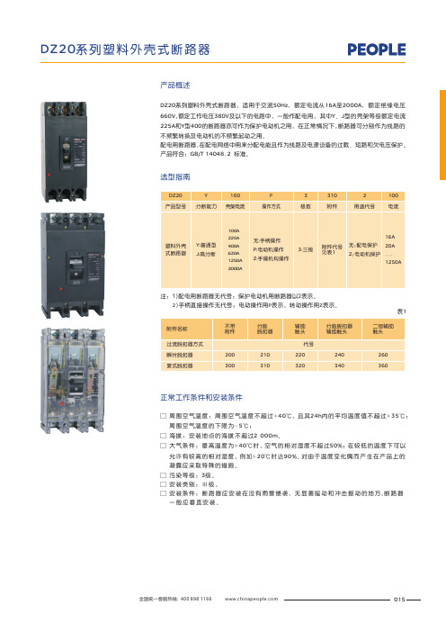
015产品概述正常工作条件和安装条件选型指南注:1)配电用断路器无代号;保护电动机用断路器以2表示。
2)手柄直接操作无代号;电动操作用P 表示,转动操作用Z 表示。
□ 周围空气温度:周围空气温度不超过+40℃,且其24h 内的平均温度值不超过+35℃; 周围空气温度的下限为-5℃;□ 海拔:安装地点的海拔不超过2 000m 。
□ 大气条件:最高温度为+40℃时,空气的相对湿度不超过50%;在较低的温度下可以 允许有较高的相对湿度,例如+20℃时达90%。
对由于温度变化偶而产生在产品上的 凝露应采取特殊的措施。
□ 污染等级:3级。
□ 安装类别:Ⅲ级。
□ 安装条件:断路器应安装在没有雨雪侵袭, 无显著摇动和冲击振动的地方,断路器 一般应垂直安装。
DZ20系列塑料外壳式断路器,适用于交流50Hz ,额定电流从16A 至2000A ,额定绝缘电压660V ,额定工作电压380V 及以下的电路中,一般作配电用,其中Y 、J 型的壳架等级额定电流225A 和Y 型400的断路器亦可作为保护电动机之用,在正常情况下,断路器可分别作为线路的不频繁转换及电动机的不频繁起动之用。
配电用断路器,在配电网络中用来分配电能且作为线路及电源设备的过载、短路和欠电压保护。
产品符合:GB/T 14048.2 标准。
表1基本参数及技术性能主电路的额定值和极限值断路器的额定值和极限值见表2控制电路分励脱扣器(Us)见表3表3表2□ 辅助触头和短路保护电器(SCPD )的协调配合辅助触头与熔断器串联(推荐选用RL6-25/6)。
在1.1 倍额定工作电压、功率因数0.5~0.7之间,能够承受熔断器熔断时间内通过预期 短路电流为1000A 。
□ 分励脱扣器动作值当电源电压等于额定控制电源电压Us 的70%~110%之间的任一电压时,则在断路器的所有操作条件下应导致分励脱扣器脱扣。
016017表5表4□ □ 配电用断路器配电用断路器在周围空气温度为+30℃下,各极同时通电时无温度补偿的反时限断开特性见表4,并应提供周围空气温度变化对特性影响 的校正曲线;□ 电动机保护用断路器电动机保护用断路器在周围空气温度为+40℃,各极同时通电时,无温度补偿的反时限断开特性见表5,并应提供周围空气温度变化对特 性影响的校正曲线。
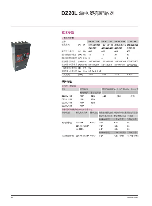
DZ20L 漏电塑壳断路器
定制剩余电流 定制分断时间
可在以下选项中任意选择三项组成可调型剩余电流(除630壳架以外)
50, 75, 100, 200, 300, 500
可在以下时间任选一项
0.1S, 0.3S, 0.4S, 0.5S,0.6S
*DZ20L-160只有4极B型才能带辅助触头
单卖附件
单卖附件 产品名称 壳架等级 附件代码
100
50 63 80 100 125 160 180 200 315 350 400 500 630
4
4: 3+N B: 4极B型
KT
KT: 100/300/500mA KR: 100/200/300mA W: 50mA Q: 75mA Y: 100mA R: 200mA T: 300mA
缺省 : 0.2s
≤60
≤80
≤100
保护特性
短路保护整定值 型号 DZ20L-160 DZ20L-250 DZ20L-400 DZ20L-630 保护类型 试验电流 配电保护 10In 10In 10In 10In 额定电流范围 电动机保护 12In 12In 12In -基准温度 特定电流整定倍数下的动作时间(电流值/起始状态) 约定不脱扣电流 约定脱扣电流 可返回 1.05In(冷态) 配电保护型 In≤63A 63A<In≤250A In>250A 电动机保护型 50A<In≤630A +40℃ +30℃ ≥1h ≥2h ≥2h 1.05In(冷态) ≥2h 1.3In(热态) <1h <2h <2h <2h 4min 3.0In(冷态) 5s 8s 8s 4s<Tp≤10s ±20 <0.2 冷态 整定值准确度% 脱扣约定时间s 起始状态
ZQN250W12RJ中文资料(Token Electronics)中文数据手册「EasyDatasheet - 矽搜」

注意事项:
●当电阻堆叠,使用焊盘圈或焊盘片,以防护证通关,提高功率要求 耗散.
芯片中文手册,看全文,戳
ZR平线绕功率电阻器
设 置 型 绕 线 ( 就 业 法 ) 40W〜 300W尺 寸
G F
I J
K D
300W
333 320 300
35 11 5.2 5.2 13 9
抵抗性
J
K
范围(Ω)
12 42 0.1~5KΩ
12 42 0.1~6KΩ
12 42 0.1~7KΩ
12 42 0.1~10KΩ
12 42 0.1~12KΩ
12 42 0.1~15KΩ
13 48 0.1~18KΩ
13 48 0.1~25KΩ
ZR平线绕功率电阻器
如何订购
ZDR
250W
250R
J
型号:ZDR ZQR ZDN ZQN
额定功率(W):40W〜300W 60W~450W 40W~300W 60W~450W
电阻值(Ω): Code 0R1
1R 10R 12R 12K
电阻值
0.1Ω 1Ω 10Ω 12Ω 12KΩ
电阻容差(%)
Code
ZR电阻适用于教育建模应用,负载测试, 产业机械,电力分配,仪器仪表,自动化控制设 备等. 该ZR系列符合RoHS标准,无铅.对于非标准技术要求和定制特殊应用,请与我们触点.
无感:
●艾尔顿·佩里型无电感线圈可用.当需要时添加"N"零件编号.
结构:
●线绕电阻器ZR是扁平形陶瓷棒有两个终端,并与绕线或者 铜线或铬合金丝作为电阻元件.
DZW中文说明书

DZW型阀门电动装置使用说明书中国扬州扬州修力设备有限公司安全该机电设备是在工业强电流的条件下使用的。
在操作中,该设备上有些裸露零件带电,同时有些零件能够运动和转动,都是危险的。
因此,未经许可拆下所需的罩盖,不合理的使用,不正确的操作或不合适的维护,均会造成严重的人身伤害或损坏设备性能。
为了设备的安全,必须保证:——仅允许有资格的人员对这些机械和设备进行作业。
——无论何时,在上述有资格的人员对该机械和设备进行作业时,他们都应具备有这些机械和设备的操作说明书或其他产品文件,以按说明书的要求执行。
——严禁没有资格的人员对该设备进行作业或在其附近进行作业。
——安装或重装后,首次电动操作,必须使阀门处于中间位置检查开关方向,必需按调试要求逐项调试,检查个部件正常后,才能投入使用。
目录1.概述 (3)2.型号表示方法 (3)3.工作环境和主要技术参数 (3)4. 外形及连接尺寸 (4)5. 结构 (5)6. 调整 (12)7. 安装与拆卸 (14)8. 故障及排除方法 (15)9. 订货须知 (15)1.概述多回转阀门电动执行机构,通称为DZW型。
适用于启闭件做直线运动的阀门,如闸阀、截止阀、隔膜阀、闸门、水闸阀等。
用于阀门的开启、关闭或调节。
是对阀门实现远控、集控和自控的必不可少的驱动装置。
他们具有功能全、性能可靠、控制系统先进、体积小、重量轻、使用维护方便等特点。
广泛用于电力、冶金、石油、化工、造纸、污水处理等行业。
多回转电动执行机构有:户外型、隔爆型、整体型、整体调节型、隔爆整体型、隔爆整体调节型等。
按连接型式,还分为转矩型和推力型。
本产品的性能符合JB/T8528-1997《普通型阀门电动装置技术条件》的规定。
隔爆型的性能符合《爆炸性气体环境用电气设备第1部分:通用要求》,《爆炸性气体环境用电气设备第2部分:隔爆型“d”》及JB/T8529-1997《隔爆型阀门电动装置技术条件》的规定。
并经国家防爆电气产品质量监督检验测试中心检定,取得了全系列的防爆合格证。
WattBox 150和250系列产品说明书

WattBox products are uniquely designed to bring unmatchedcontrol and troubleshooting to your most frequently used devices. And with the ultra-compact 150- and 250-Series, your integrator can place them just about anywhere. We even offer a Wi-Fi option to help expand your connectivity without the look of messy cables or wires. LO W P RO F I L E If you love the idea of managing your network devices and other electronics through an app, but hate the look of a bulky power strip, then the WattBox 150 and 250 are the perfectadditions to your technology setup. Theseminimalist power devices fit easily behind orunder furniture, on the back of a TV, or undera desk.S E L F -H E A L I N GWattBox products are uniquely designedto fix themselves without any outsideintervention, keeping you from having to callyour integrator and schedule an appointment.The unit continuously troubleshoots andaddresses issues before they become a largerproblem.TA K E C O N T RO LWith your WattBox purchase, you’ll receiveaccess to an intuitive remote managementmobile app. The interface is easy to navigateand lets you reboot your device with the pushof a button, getting you back online in no time.Plus, if you ever need to reach your installer,you can access their contact information easily within the app. Small & MightyWB-150-250-071519。
ZXTP25020DFLTA;中文规格书,Datasheet资料

ZXTP25020DFL20V, SOT23, PNP low power transistorSummaryBV CEO > -20V BV ECO > -4V I C(cont) = 1.5AV CE(sat) < 85 mV @ 1A R CE(sat) = 54m ⍀P D = 350mWComplementary part number ZXTN25020DFLDescriptionAdvanced process capability has been used to achieve high current gain hold up making this device ideal for applications requiring high pulse currents.Features•High peak current •Low saturation voltageApplications•DC-DC converters•MOSFET and IGBT gate drivingOrdering informationDevice marking1F2DeviceReel size (inches)Tape width (mm)Quantity per reelZXTP25020DFLTA783000Absolute maximum ratingsParameter Symbol Limit Unit Collector-base voltage V CBO-25V Collector-emitter voltage (forward blocking)V CEO-20V Emitter-collector voltage (reverse blocking)V ECO -4V Emitter-base voltage V EBO -7V Continuous collector current I C-1.5A Base current I B-500mA Peak pulse current I CM-6A Power dissipation at T amb =25°C(a)P D 350mW Linear derating factor 2.8mW/°C Operating and storage temperature range T j, T stg -55 to 150°C Thermal resistanceParameter Symbol Limit Unit Junction to ambient(a)R⍜JA357°C/WNOTES:(a)For a device surface mounted on 25mm x 25mm x 1.6mm FR4 PCB with high coverage of single sided 1oz copper, instill air conditions.CharacteristicsElectrical characteristics (at T amb = 25°C unless otherwise stated)ParameterSymbol Min.Typ.Max.Unit Conditions Collector-base breakdown voltageBV CBO -25-55V I C = -100A Collector-emitter breakdown voltage (base open)BV CEO -20-45V I C = -10mA (*)NOTES:(*)Measured under pulsed conditions. Pulse width Յ300s; duty cycle Յ2%.Emitter-base breakdown voltageBV EBO -7-8.3V I E = -100A Emitter-collector breakdown voltage (reverse blocking)BV ECO -4-8.5V I E = -100uA (*)Collector cut-off currentI CBO<-1-50nA V CB = -20V-20A V CB = -20V, T amb = 100°C Emitter cut-off current I EBO <-1-50nA V EB = -5.6VCollector-emitter saturation voltageV CE(sat)-65-85mV I C = -1A, I B = -100mA (*)-160-225mV I C = -1A, I B = -10mA (*)150-195mV I C = -1.5A, I B = -30mA (*)-210-275mV I C = -2A, I B = -40mA (*)-215260mV I C = -4A, I B = -400mA (*)Base-emitter saturation voltage V BE(sat)-845-950mV I C = -1.5A, I B = -30mA (*)Base-emitter turn-on voltageV BE(on)-785-900mVI C = -1.5A, V CE = -2V (*)Static forward current transfer ratioh FE 300450900I C = -10mA, V CE = -2V (*)160250I C = -1.5A, V CE = -2V (*)6090I C = -4A, V CE = -2V (*)15I C = -10A, V CE = -2V (*)Transition frequency f T 290MHz I C = -50mA, V CE = -10Vf = 50MHz Output capacitance C obo 2130pFV CB = -10V, f = 1MHz (*)Delay time t (d)14.2V CC = -10V. I C = -1A, I B1 = I B2= -50mA.Rise time t (r)16.3Storage time t (s)186Fall timet (f)32.7Package outline - SOT23Note: Controlling dimensions are in millimeters. Approximate dimensions are provided in incheslimeters Inches limeters Inches Min.Max.Min.Max.Min.Max.Max.Max.A - 1.12-0.044e1 1.90 NOM0.075 NOMA10.010.100.00040.004E 2.10 2.640.0830.104b 0.300.500.0120.020E1 1.20 1.400.0470.055C 0.0850.1200.0030.008L 0.250.620.0180.024D 2.803.040.1100.120L10.450.620.0180.024e0.95 NOM 0.0375 NOM-----Intentionally left blankZetex sales offices EuropeZetex GmbHKustermann-park Balanstraße 59D-81541 München GermanyTelefon: (49) 89 45 49 49 0Fax: (49) 89 45 49 49 49europe.sales@AmericasZetex Inc700 Veterans Memorial Highway Hauppauge, NY 11788USATelephone: (1) 631 360 2222Fax: (1) 631 360 8222usa.sales@Asia PacificZetex (Asia Ltd)3701-04 Metroplaza Tower 1Hing Fong Road, Kwai Fong Hong KongTelephone: (852) 26100 611Fax: (852) 24250 494asia.sales@Corporate HeadquartersZetex Semiconductors plcZetex Technology Park, Chadderton Oldham, OL9 9LL United KingdomTelephone: (44) 161 622 4444Fax: (44) 161 622 4446hq@© 2007 Published by Zetex Semiconductors plcDefinitionsProduct changeZetex Semiconductors reserves the right to alter, without notice, specifications, design, price or conditions of supply of any product or service. Customers are solely responsible for obtaining the latest relevant information before placing orders.Applications disclaimerThe circuits in this design/application note are offered as design ideas. It is the responsibility of the user to ensure that the circuit is fit for the user’s application and meets with the user’s requirements. No representation or warranty is given and no liability whatsoever is assumed by Zetex with respect to the accuracy or use of such information, or infringement of patents or other intellectual property rights arising from such use or otherwise. Zetex does not assume any legal responsibility or will not be held legally liable (whether in contract,tort (including negligence), breach of statutory duty, restriction or otherwise) for any damages, loss of profit, business, contract,opportunity or consequential loss in the use of these circuit applications, under any circumstances.Life supportZetex products are specifically not authorized for use as critical components in life support devices or systems without the express written approval of the Chief Executive Officer of Zetex Semiconductors plc. As used herein:A. Life support devices or systems are devices or systems which:1.are intended to implant into the body or2.support or sustain life and whose failure to perform when properly used in accordance with instructions for use provided in the labeling can be reasonably expected to result in significant injury to the user.B. A critical component is any component in a life support device or system whose failure to perform can be reasonably expected tocause the failure of the life support device or to affect its safety or effectiveness.ReproductionThe product specifications contained in this publication are issued to provide outline information only which (unless agreed by the company in writing) may not be used, applied or reproduced for any purpose or form part of any order or contract or be regarded as a representation relating to the products or services concerned. Terms and ConditionsAll products are sold subjects to Zetex’ terms and conditions of sale, and this disclaimer (save in the event of a conflict between the two when the terms of the contract shall prevail) according to region, supplied at the time of order acknowledgement.For the latest information on technology, delivery terms and conditions and prices, please contact your nearest Zetex sales office.Quality of productZetex is an ISO 9001 and TS16949 certified semiconductor manufacturer.To ensure quality of service and products we strongly advise the purchase of parts directly from Zetex Semiconductors or one of our regionally authorized distributors. For a complete listing of authorized distributors please visit: /salesnetworkZetex Semiconductors does not warrant or accept any liability whatsoever in respect of any parts purchased through unauthorized sales channels.ESD (Electrostatic discharge)Semiconductor devices are susceptible to damage by ESD. Suitable precautions should be taken when handling and transporting devices.The possible damage to devices depends on the circumstances of the handling and transporting, and the nature of the device. The extent of damage can vary from immediate functional or parametric malfunction to degradation of function or performance in use over time.Devices suspected of being affected should be replaced.Green complianceZetex Semiconductors is committed to environmental excellence in all aspects of its operations which includes meeting or exceeding reg-ulatory requirements with respect to the use of hazardous substances. Numerous successful programs have been implemented to reduce the use of hazardous substances and/or emissions.All Zetex components are compliant with the RoHS directive, and through this it is supporting its customers in their compliance with WEEE and ELV directives.Product status key:“Preview”Future device intended for production at some point. Samples may be available “Active”Product status recommended for new designs “Last time buy (LTB)”Device will be discontinued and last time buy period and delivery is in effect “Not recommended for new designs”Device is still in production to support existing designs and production “Obsolete”Production has been discontinued Datasheet status key:“Draft version”This term denotes a very early datasheet version and contains highly provisional information, whichmay change in any manner without notice.“Provisional version”This term denotes a pre-release datasheet. It provides a clear indication of anticipated performance.However, changes to the test conditions and specifications may occur, at any time and without notice.“Issue”This term denotes an issued datasheet containing finalized specifications. However, changes tospecifications may occur, at any time and without notice.分销商库存信息: DIODESZXTP25020DFLTA。
一部分小型断路器和塑壳断路器的使用说明

一部分小型断路器和塑壳断路器的使用说明DZ15系列塑料外壳式断路器DZ15系列塑料外壳式断路器适用于交流50hz、额定电压380v、额定电流至63a (100)的电路中作为通断操作,并可用来保护线路和电动机的过载及短路保护之用,亦可作为线路的不频繁转换及电动机的不频繁起动之用。
DZ20系列塑料外壳式断路器适用于交流50hz,额定绝缘电压660v,额定工作电压380v(400v)及以下,其额定电流至1250a . 一般作为配电用,额定电流200a和400y型的断路器亦可作为保护电动机用。
在正常情况下,断路器可分别作为线路不频繁转换及电动机的不频繁起动之用。
四极断路器主要用于交流50hz、额定电压400v及以下,额定电流100至630a 三相五线制的系统中,它能保证用户和电源完全断开,确保安全,从而解决其它任何断路器不可克服的中性极电流不为零的弊端。
配电用断路器在配电网络中用来分配电能,且可作为线路及电源设备的过载、短路和欠电压保护。
保护电动机用断路器在配电网络中用作鼠笼型电动机的起动和分断以及作为电动机的过载、短路和欠电压保护。
DZ47系列小型断路器DZ47系列小型断路器主要适用于交流50hz/60hz,额定工作电压为240v/415v及以下,额定电流至60a的电路中,该断路器主要用于现代建筑物的电气线路及设备的过载,短路保护,亦适用于线路的不频繁操作及隔离SCM1(cm1)系列断路器SCM1(cm1)系列断路器适用于交流50hz、60hz、500v及以下的电路中作不频繁转换和电动机不频繁起动之用。
断路器具有过载、短路和欠电压保护装置,能保护线路及电源设备不受损坏。
本断路可垂直安装、亦可水平安装。
DW10系列万能式断路器DW10系列万能式断路器适用于交流50hz、电压至380v、直流电压至440v的电气线路中,作过载、短路、失压保护以及正常条件下的不频繁转换之用。
当三极断路器在直流电路中串联使用时,电压允许提高至440v.DW15系列万能式空气断路器适用于交流50hz、额定电流至4000a,额定工作电压至1140v(壳架等级额定电流630a以下)80v(壳架等级额定电流1000a及以上)的配电网络中,用来分配电能和供电线路及电源设备的过载、欠电压、短路保护之用。
- 1、下载文档前请自行甄别文档内容的完整性,平台不提供额外的编辑、内容补充、找答案等附加服务。
- 2、"仅部分预览"的文档,不可在线预览部分如存在完整性等问题,可反馈申请退款(可完整预览的文档不适用该条件!)。
- 3、如文档侵犯您的权益,请联系客服反馈,我们会尽快为您处理(人工客服工作时间:9:00-18:30)。
ZXTP25020DZ20V PNP high gain transistor in SOT89SummaryBV CEO > -20V BV ECO > -4V I C(cont) = 5AV CE(sat) < -65mV @ -1A R CE(sat) = 39m ⍀ P D = 2.4WComplementary part number ZXTN25020DZDescriptionPackaged in the SOT89 outline this new low saturation 20V PNP transistor offers extremely low on state losses making it ideal for use in DC-DC circuits and various driving and power management functionsFeatures•High peak current •Low saturation voltage •High gain •SOT89 packageApplications•DC-DC converters •Load switch •Motor drive •Disconnect switch•MOSFET and IGBT gate driveOrdering informationDevice marking•1L5DeviceReel size(inches)Tape width (mm)Quantity per reel ZXTP25020DZTA7121000Absolute maximum ratingsThermal resistanceNOTES:(a)For a device surface mounted on 15mm x 15mm x 0.6mm FR4 PCB with high coverage of single sided 1oz copper, in still air conditions.(b)Mounted on 25mm x 25mm x 0.6mm FR4 PCB with high coverage of single sided 1oz copper, in still air conditions.(c)Mounted on 50mm x 50mm x 0.6mm FR4 PCB with high coverage of single sided 2oz copper, in still air conditions.(d)As (c) above measured at t<5 seconds.(e)Junction to case (collector tab). Typical.ParameterSymbol Limit Unit Collector-Base voltage V CBO -25V Collector-Emitter voltageV CEO -20V Emitter-Base voltage (reverse blocking)V ECO -4V Emitter-Base voltageV EBO -7V Continuous Collector current (c)I C -5A Base current I B -1A Peak pulse currentI CM -10A Power dissipation at T A =25°C (a)Linear derating factorP D1.18.8W mW/°C Power dissipation at T A =25°C (b)Linear derating factorP D 1.814.4W mW/°C Power dissipation at T A =25°C (c)Linear derating factorP D 2.419.2W mW/°C Power dissipation at T A =25°C (d)Linear derating factorP D 4.4635.7W mW/°C Power dissipation at T C =25°C (e)Linear derating factorP D 15.7126W mW/°C Operating and storage temperature rangeT j , T stg -55 to 150°CParameterSymbol Limit Unit Junction to ambient (a)R ⍜JA 117°C/W Junction to ambient (b)R ⍜JA 68°C/W Junction to ambient (c)R ⍜JA 51°C/W Junction to ambient (d)R ⍜JA 28°C/W Junction to case (e)R ⍜JC7.95°C/WElectrical characteristics (at T amb = 25°C unless otherwise stated)ParameterSymbol Min.Typ.Max.Unit Conditions Collector-Base breakdown voltageBV CBO -25-55V I C = -100μA Collector-Emitter breakdown voltage BV CEO -20-45V I C = -10mA (*)NOTES:(*)Measured under pulsed conditions. Pulse width ≤ 300µs; duty cycle ≤ 2%.Emitter-Collector breakdown voltage (reverse blocking)BV ECX -4-8.5V I E = -100μA, R BC < 1k Ω or 0.25V > V BC > -0.25V Emitter-Collector breakdown voltage (reverse blocking)BV ECO -4-8.5V I E = -100μA Emitter-Base breakdown voltageBV EBO -7-8.3V I E = -5.6VCollector-Base cut-off currentI CBO <1-50-0.5nA μA V CB = -25VV CB = -25V , T amb =100°C Emitter cut-off current I EBO <1-50nA V EB = -5.6VCollector-Emitter saturation voltageV CE(sat)-50-150-185-195-65-215-245-265mV mV mV mV I C = -1A, I B = -100mA (*)I C = -1A, I B = -10mA (*)I C = -2A, I B = -40mA (*)I C = -5A, I B = -500mA (*)Base-Emitter saturation voltageV BE(sat)-1010-1100mV I C = -5A, I B = -500mA (*)Base-Emitter turn-on voltageV BE(on)-870-1000mVI C = -5A, V CE = -2V (*)Static forward current transfer ratioh FE300200454503108520900I C = -10mA, V CE = -2V (*)I C = -1A, V CE = -2V (*) I C = -5A, V CE = -2V (*)I C = -10A, V CE = -2V (*)Transition frequency f T 290MHz I C = -50mA, V CE = -10V f = 100MHzInput capacitance C ibo 157400pF V EB = -0.5V, f = 1MHz (*)Output capacitance C obo 2130pF V CB = -10V, f = 1MHz (*)Delay time t d 14.2ns V CC = -10V, I C = -1A, I B1 = -I B2 = -50mA Rise time t r 16.3ns Storage time t s 186ns Fall timet f32.7nsPackage outline - SOT89DIM Millimeters Inches DIM Millimeters Inches Min Max Min Max Min Max Min MaxA 1.40 1.600.5500.630E 2.29 2.600.0900.102B0.440.560.0170.022E1 2.13 2.290.0840.090 B10.360.480.0140.019e 1.50 BSC0.059 BSC C0.350.440.0140.017e1 3.00 BSC0.118 BSCD 4.40 4.600.1730.181H 3.94 4.250.1550.167D1 1.52 1.830.0640.072L0.89 1.200.0350.047 Note: Controlling dimensions are in millimeters. Approximate dimensions are provided in inchesZetex sales offices EuropeZetex GmbHKustermann-park Balanstraße 59D-81541 München GermanyTelefon: (49) 89 45 49 49 0Fax: (49) 89 45 49 49 49europe.sales@AmericasZetex Inc700 Veterans Memorial Highway Hauppauge, NY 11788USATelephone: (1) 631 360 2222Fax: (1) 631 360 8222usa.sales@Asia PacificZetex (Asia Ltd)3701-04 Metroplaza Tower 1Hing Fong Road, Kwai Fong Hong KongTelephone: (852) 26100 611Fax: (852) 24250 494asia.sales@Corporate HeadquartersZetex Semiconductors plcZetex Technology Park, Chadderton Oldham, OL9 9LL United KingdomTelephone: (44) 161 622 4444Fax: (44) 161 622 4446hq@© 2007 Published by Zetex Semiconductors plcDefinitionsProduct changeZetex Semiconductors reserves the right to alter, without notice, specifications, design, price or conditions of supply of any product or service. Customers are solely responsible for obtaining the latest relevant information before placing orders.Applications disclaimerThe circuits in this design/application note are offered as design ideas. It is the responsibility of the user to ensure that the circuit is fit for the user’s application and meets with the user’s requirements. No representation or warranty is given and no liability whatsoever is assumed by Zetex with respect to the accuracy or use of such information, or infringement of patents or other intellectual property rights arising from such use or otherwise. Zetex does not assume any legal responsibility or will not be held legally liable (whether in contract,tort (including negligence), breach of statutory duty, restriction or otherwise) for any damages, loss of profit, business, contract,opportunity or consequential loss in the use of these circuit applications, under any circumstances.Life supportZetex products are specifically not authorized for use as critical components in life support devices or systems without the express written approval of the Chief Executive Officer of Zetex Semiconductors plc. As used herein:A. Life support devices or systems are devices or systems which:1.are intended to implant into the body or2.support or sustain life and whose failure to perform when properly used in accordance with instructions for use provided in the labeling can be reasonably expected to result in significant injury to the user.B. A critical component is any component in a life support device or system whose failure to perform can be reasonably expected tocause the failure of the life support device or to affect its safety or effectiveness.ReproductionThe product specifications contained in this publication are issued to provide outline information only which (unless agreed by the company in writing) may not be used, applied or reproduced for any purpose or form part of any order or contract or be regarded as a representation relating to the products or services concerned. Terms and ConditionsAll products are sold subjects to Zetex’ terms and conditions of sale, and this disclaimer (save in the event of a conflict between the two when the terms of the contract shall prevail) according to region, supplied at the time of order acknowledgement.For the latest information on technology, delivery terms and conditions and prices, please contact your nearest Zetex sales office.Quality of productZetex is an ISO 9001 and TS16949 certified semiconductor manufacturer.To ensure quality of service and products we strongly advise the purchase of parts directly from Zetex Semiconductors or one of our regionally authorized distributors. For a complete listing of authorized distributors please visit: /salesnetworkZetex Semiconductors does not warrant or accept any liability whatsoever in respect of any parts purchased through unauthorized sales channels.ESD (Electrostatic discharge)Semiconductor devices are susceptible to damage by ESD. Suitable precautions should be taken when handling and transporting devices.The possible damage to devices depends on the circumstances of the handling and transporting, and the nature of the device. The extent of damage can vary from immediate functional or parametric malfunction to degradation of function or performance in use over time.Devices suspected of being affected should be replaced.Green complianceZetex Semiconductors is committed to environmental excellence in all aspects of its operations which includes meeting or exceeding reg-ulatory requirements with respect to the use of hazardous substances. Numerous successful programs have been implemented to reduce the use of hazardous substances and/or emissions.All Zetex components are compliant with the RoHS directive, and through this it is supporting its customers in their compliance with WEEE and ELV directives.Product status key:“Preview”Future device intended for production at some point. Samples may be available “Active”Product status recommended for new designs “Last time buy (LTB)”Device will be discontinued and last time buy period and delivery is in effect “Not recommended for new designs”Device is still in production to support existing designs and production “Obsolete”Production has been discontinued Datasheet status key:“Draft version”This term denotes a very early datasheet version and contains highly provisional information, whichmay change in any manner without notice.“Provisional version”This term denotes a pre-release datasheet. It provides a clear indication of anticipated performance.However, changes to the test conditions and specifications may occur, at any time and without notice.“Issue”This term denotes an issued datasheet containing finalized specifications. However, changes tospecifications may occur, at any time and without notice.分销商库存信息: DIODESZXTP25020DZTA。