74ALVC08MX_NL中文资料
HD74ALVC2G08US中文资料

Item Propagation delay time
•
VCC = 3.3±0.3 V
Symbol tPLH tPHL Min 1.0 Typ Max 2.8 Unit ns Test conditions CL = 30 pF FROM (Input) A or B TO (Output) Y
Conditions
Output voltage range
Output : H or L VCC : OFF
Input clamp current Output clamp current Continuous output current Continuous current through VCC or GND Maximum power dissipation *3 at Ta = 25°C (in still air) Storage temperature Notes:
Package type SSOP-8 pin Package code TTP-8DB Package suffix US Taping code E (3,000 pcs / Reel)
HD74ALVC2G08
Outline and Article Indication
• HD74ALVC2G08
µA µA µA pF
VIN = 3.6 V or GND VIN = VCC or GND, IO = 0 VIN or VO = 0 to 3.6 V VIN = VCC or GND
Note: For conditions shown as Min or Max, use the appropriate values under recommended operating conditions.
LVC08A中文资料

元器件交易网SO14:plastic small outline package; 14 leads; body width 3.9 mm SOT108-1SSOP14:plastic shrink small outline package; 14 leads; body width 5.3 mm SOT337-1TSSOP14:plastic thin shrink small outline package; 14 leads; body width 4.4 mm SOT402-1Philips Semiconductors and Philips Electronics North America Corporation reserve the right to make changes, without notice, in the products,including circuits, standard cells, and/or software, described or contained herein in order to improve design and/or performance. Philips Semiconductors assumes no responsibility or liability for the use of any of these products, conveys no license or title under any patent, copyright,or mask work right to these products, and makes no representations or warranties that these products are free from patent, copyright, or mask work right infringement, unless otherwise specified. Applications that are described herein for any of these products are for illustrative purposes only. Philips Semiconductors makes no representation or warranty that such applications will be suitable for the specified use without further testing or modification.LIFE SUPPORT APPLICATIONS Philips Semiconductors and Philips Electronics North America Corporation Products are not designed for use in life support appliances, devices,or systems where malfunction of a Philips Semiconductors and Philips Electronics North America Corporation Product can reasonably be expected to result in a personal injury. Philips Semiconductors and Philips Electronics North America Corporation customers using or selling Philips Semiconductors and Philips Electronics North America Corporation Products for use in such applications do so at their own risk and agree to fully indemnify Philips Semiconductors and Philips Electronics North America Corporation for any damages resulting from such improper use or sale.This data sheet contains preliminary data, and supplementary data will be published at a later date. PhilipsSemiconductors reserves the right to make changes at any time without notice in order to improve designand supply the best possible product.Philips Semiconductors811 East Arques AvenueP .O. Box 3409Sunnyvale, California 94088–3409Telephone 800-234-7381DEFINITIONSData Sheet IdentificationProduct Status Definition Objective Specification Preliminary Specification Product Specification Formative or in Design Preproduction Product Full ProductionThis data sheet contains the design target or goal specifications for product development. Specificationsmay change in any manner without notice.This data sheet contains Final Specifications. Philips Semiconductors reserves the right to make changesat any time without notice, in order to improve design and supply the best possible product.© Copyright Philips Electronics North America Corporation 1997All rights reserved. Printed in U.S.A.print codeDate of release: 05-96。
74LS08中文资料_数据手册_参数

5
PACKAGE OPTION ADDENDUM
PACKAGING INFORMATION
Orderable Device JM38510/08003BCA
Status Package Type Package Pins Package
(1)
Drawing
Qty
ACTIVE
CDIP
1
TBD
J
14
1
TBD
N
14
TBD
N
14
TBD
N
14
TBD
N
14
TBD
D
14
50 Green (RoHS
& no Sb/Br)
D
14
50 Green (RoHS
& no Sb/Br)
Lead/Ball Finish
(6)
POST-PLATE
POST-PLATE
A42
A42
A42
A42
A42
A42
A42
N / A for Pkg Type -55 to 125
N / A for Pkg Type -55 to 125
N / A for Pkg Type -55 to 125
N / A for Pkg Type -55 to 125
N / A for Pkg Type -55 to 125
N / A for Pkg Type -55 to 125
N / A for Pkg Type -55 to 125
N / A for Pkg Type -55 to 125
N / A for Pkg Type
N / A for Pkg Type
multisim元件中英文对照

multisim 元件名称对照元件名称中文名说明7407 驱动门1N914 二极管74Ls00 与非门74LS04 非门74LS08 与门74LS390 TTL 双十进制计数器7SEG 4针BCD-LED 输出从0-9 对应于4根线的BCD码7SEG 3-8译码器电路BCD-7SEG[size=+0]转换电路ALTERNA TOR 交流发电机AMMETER-MILLI mA安培计AND 与门BA TTERY电池/电池组BUS 总线CAP 电容CAPACITOR 电容器CLOCK 时钟信号源CRYSTAL 晶振D-FLIPFLOP D触发器FUSE 保险丝GROUND 地LAMP 灯LED-RED 红色发光二极管LM016L 2行16列液晶可显示2行16列英文字符,有8位数据总线D0-D7,RS,R/W,EN三个控制端口(共14线),工作电压为5V。
没背光,和常用的1602B功能和引脚一样(除了调背光的二个线脚)LOGIC ANALYSER 逻辑分析器LOGICPROBE 逻辑探针LOGICPROBE[BIG] 逻辑探针用来显示连接位置的逻辑状态LOGICSTA TE 逻辑状态用鼠标点击,可改变该方框连接位置的逻辑状态LOGICTOGGLE 逻辑触发MASTERSWITCH 按钮手动闭合,立即自动打开MOTOR 马达OR 或门POT-LIN 三引线可变电阻器POWER 电源RES 电阻RESISTOR 电阻器SWITCH 按钮手动按一下一个状态SWITCH-SPDT 二选通一按钮VOLTMETER 伏特计VOLTMETER-MILLI mV伏特计VTERM 串行口终端Electromechanical 电机Inductors 变压器Laplace Primitives 拉普拉斯变换Memory IcsMicroprocessor IcsMiscellaneous 各种器件AERIAL-天线;A TAHDD;A TMEGA64;BA TTERY;CELL;CRYSTAL-晶振;FUSE;METER-仪表;Modelling Primitives 各种仿真器件是典型的基本元器模拟,不表示具体型号,只用于仿真,没有PCBOptoelectronics 各种发光器件发光二极管,LED,液晶等等PLDs & FPGAsResistors 各种电阻Simulator Primitives 常用的器件Speakers & SoundersSwitches & Relays 开关,继电器,键盘Switching Devices 晶阊管Transistors 晶体管(三极管,场效应管)TTL 74 seriesTTL 74ALS seriesTTL 74AS seriesTTL 74F seriesTTL 74HC seriesTTL 74HCT seriesTTL 74LS seriesTTL 74S seriesAnalog Ics 模拟电路集成芯片Capacitors 电容集合CMOS 4000 seriesConnectors 排座,排插Data Converters ADC,DACDebugging Tools 调试工具ECL 10000 Series------------------------------------------------------------PROTEUS元件库元件名称及中英对照AND 与门ANTENNA天线BA TTERY直流电源BELL 铃,钟BVC 同轴电缆接插件BRIDEG 1 整流桥(二极管)BRIDEG 2 整流桥(集成块)BUFFER 缓冲器BUZZER 蜂鸣器CAP 电容CAPACITOR 电容CAPACITOR POL 有极性电容CAPV AR 可调电容CIRCUIT BREAKER 熔断丝COAX 同轴电缆CON 插口CRYSTAL 晶体整荡器DB 并行插口DIODE 二极管DIODE SCHOTTKY稳压二极管DIODE V ARACTOR 变容二极管DPY_3-SEG 3段LEDDPY_7-SEG 7段LEDDPY_7-SEG_DP 7段LED(带小数点) ELECTRO 电解电容FUSE 熔断器INDUCTOR 电感INDUCTOR IRON 带铁芯电感INDUCTOR3 可调电感JFET N N沟道场效应管JFET P P沟道场效应管LAMP 灯泡LAMP NEDN 起辉器LED 发光二极管METER 仪表MICROPHONE 麦克风MOSFET MOS管MOTOR AC 交流电机MOTOR SERVO 伺服电机NAND 与非门NOR 或非门NOT 非门NPN NPN三极管NPN-PHOTO 感光三极管OPAMP 运放OR 或门PHOTO 感光二极管PNP 三极管NPN DAR NPN三极管PNP DAR PNP三极管POT 滑线变阻器PELAY-DPDT 双刀双掷继电器RES1.2 电阻RES3.4 可变电阻RESISTOR BRIDGE ? 桥式电阻RESPACK ? 电阻SCR 晶闸管PLUG ? 插头PLUG AC FEMALE 三相交流插头SOCKET ? 插座SOURCE CURRENT 电流源SOURCE VOLTAGE 电压源SPEAKER 扬声器SW ? 开关SW-DPDY ? 双刀双掷开关SW-SPST ? 单刀单掷开关SW-PB 按钮THERMISTOR 电热调节器TRANS1 变压器TRANS2 可调变压器TRIAC ? 三端双向可控硅TRIODE ? 三极真空管V ARISTOR 变阻器ZENER ? 齐纳二极管DPY_7-SEG_DP 数码管SW-PB 开关----------------------------------------------------------------------PROTEUS原理图元器件库详细说明Device.lib 包括电阻、电容、二极管、三极管和PCB的连接器符号ACTIVE.LIB 包括虚拟仪器和有源器件DIODE.LIB 包括二极管和整流桥DISPLAY.LIB 包括LCD、LEDBIPOLAR.LIB 包括三极管FET.LIB 包括场效应管ASIMMDLS.LIB 包括模拟元器件V ALVES .LIB 包括电子管ANALOG.LIB 包括电源调节器、运放和数据采样IC CAPACITORS.LIB 包括电容COMS.LIB 包括4000系列ECL.LIB 包括ECL10000系列MICRO.LIB 包括通用微处理器OPAMP.LIB 包括运算放大器RESISTORS.LIB 包括电阻FAIRCHLD .LIB 包括FAIRCHLD 半导体公司的分立器件LINTEC.LIB 包括LINTEC公司的运算放大器NA TDAC.LIB 包括国家半导体公司的数字采样器件NA TOA.LIB 包括国家半导体公司的运算放大器TECOOR.LIB 包括TECOOR公司的SCR 和TRIAC TEXOAC.LIB 包括德州仪器公司的运算放大器和比较器ZETEX .LIB 包括ZETEX 公司的分立器件。
74系列芯片功能表汇总
74系列芯片功能表汇总74系列标准数字电路功能表——中文资料名称类别功能7400 TTL 2输入端四与非门7401 TTL 集电极开路2输入端四与非门7402 TTL 2输入端四或非门7403 TTL 集电极开路2输入端四与非门7404 TTL 六反相器7405 TTL 集电极开路六反相器7406 TTL 集电极开路六反相高压驱动器7407 TTL 集电极开路六正相高压驱动器7408 TTL 2输入端四与门7409 TTL 集电极开路2输入端四与门7410 TTL 3输入端3与非门74107 TTL 带清除主从双J-K触发器74109 TTL 带预置清除正触发双J-K触发器7411 TTL 3输入端3与门74112 TTL 带预置清除负触发双J-K触发器7412 TTL 开路输出3输入端三与非门74121 TTL 单稳态多谐振荡器74122 TTL 可再触发单稳态多谐振荡器74123 TTL 双可再触发单稳态多谐振荡器74125 TTL 三态输出高有效四总线缓冲门74126 TTL 三态输出低有效四总线缓冲门7413 TTL 4输入端双与非施密特触发器74132 TTL 2输入端四与非施密特触发器74133 TTL 13输入端与非门74136 TTL 四异或门74138 TTL 3-8线译码器/复工器74139 TTL 双2-4线译码器/复工器7414 TTL 六反相施密特触发器74145 TTL BCD—十进制译码/驱动器7415 TTL 开路输出3输入端三与门74150 TTL 16选1数据选择/多路开关74151 TTL 8选1数据选择器74153 TTL 双4选1数据选择器74154 TTL 4线—16线译码器74155 TTL 图腾柱输出译码器/分配器74156 TTL 开路输出译码器/分配器74157 TTL 同相输出四2选1数据选择器74158 TTL 反相输出四2选1数据选择器7416 TTL 开路输出六反相缓冲/驱动器74160 TTL 可预置BCD异步清除计数器74161 TTL 可予制四位二进制异步清除计数器74162 TTL 可预置BCD同步清除计数器74163 TTL 可予制四位二进制同步清除计数器74164 TTL 八位串行入/并行输出移位寄存器74165 TTL 八位并行入/串行输出移位寄存器74166 TTL 八位并入/串出移位寄存器74169 TTL 二进制四位加/减同步计数器7417 TTL 开路输出六同相缓冲/驱动器74170 TTL 开路输出4×4寄存器堆74173 TTL 三态输出四位D型寄存器74174 TTL 带公共时钟和复位六D触发器74175 TTL 带公共时钟和复位四D触发器74180 TTL 9位奇数/偶数发生器/校验器74181 TTL 算术逻辑单元/函数发生器74185 TTL 二进制—BCD代码转换器74190 TTL BCD同步加/减计数器74191 TTL 二进制同步可逆计数器74192 TTL 可预置BCD双时钟可逆计数器74193 TTL 可预置四位二进制双时钟可逆计数器74194 TTL 四位双向通用移位寄存器74195 TTL 四位并行通道移位寄存器74196 TTL 十进制/二-十进制可预置计数锁存器74197 TTL 二进制可预置锁存器/计数器7420 TTL 4输入端双与非门7421 TTL 4输入端双与门7422 TTL 开路输出4输入端双与非门74221 TTL 双/单稳态多谐振荡器74240 TTL 八反相三态缓冲器/线驱动器74241 TTL 八同相三态缓冲器/线驱动器74243 TTL 四同相三态总线收发器74244 TTL 八同相三态缓冲器/线驱动器74245 TTL 八同相三态总线收发器74247 TTL BCD—7段15V输出译码/驱动器74248 TTL BCD—7段译码/升压输出驱动器74249 TTL BCD—7段译码/开路输出驱动器74251 TTL 三态输出8选1数据选择器/复工器74253 TTL 三态输出双4选1数据选择器/复工器74256 TTL 双四位可寻址锁存器74257 TTL 三态原码四2选1数据选择器/复工器74258 TTL 三态反码四2选1数据选择器/复工器74259 TTL 八位可寻址锁存器/3-8线译码器7426 TTL 2输入端高压接口四与非门74260 TTL 5输入端双或非门74266 TTL 2输入端四异或非门7427 TTL 3输入端三或非门74273 TTL 带公共时钟复位八D触发器74279 TTL 四图腾柱输出S-R锁存器7428 TTL 2输入端四或非门缓冲器74283 TTL 4位二进制全加器74290 TTL 二/五分频十进制计数器74293 TTL 二/八分频四位二进制计数器74295 TTL 四位双向通用移位寄存器74298 TTL 四2输入多路带存贮开关74299 TTL 三态输出八位通用移位寄存器7430 TTL 8输入端与非门7432 TTL 2输入端四或门74322 TTL 带符号扩展端八位移位寄存器74323 TTL 三态输出八位双向移位/存贮寄存器7433 TTL 开路输出2输入端四或非缓冲器74347 TTL BCD—7段译码器/驱动器74352 TTL 双4选1数据选择器/复工器74353 TTL 三态输出双4选1数据选择器/复工器74365 TTL 门使能输入三态输出六同相线驱动器74365 TTL 门使能输入三态输出六同相线驱动器74366 TTL 门使能输入三态输出六反相线驱动器74367 TTL 4/2线使能输入三态六同相线驱动器74368 TTL 4/2线使能输入三态六反相线驱动器7437 TTL 开路输出2输入端四与非缓冲器74373 TTL 三态同相八D锁存器74374 TTL 三态反相八D锁存器74375 TTL 4位双稳态锁存器74377 TTL 单边输出公共使能八D锁存器74378 TTL 单边输出公共使能六D锁存器74379 TTL 双边输出公共使能四D锁存器7438 TTL 开路输出2输入端四与非缓冲器74380 TTL 多功能八进制寄存器7439 TTL 开路输出2输入端四与非缓冲器74390 TTL 双十进制计数器74393 TTL 双四位二进制计数器7440 TTL 4输入端双与非缓冲器7442 TTL BCD—十进制代码转换器74352 TTL 双4选1数据选择器/复工器74353 TTL 三态输出双4选1数据选择器/复工器74365 TTL 门使能输入三态输出六同相线驱动器74366 TTL 门使能输入三态输出六反相线驱动器74367 TTL 4/2线使能输入三态六同相线驱动器74368 TTL 4/2线使能输入三态六反相线驱动器7437 TTL 开路输出2输入端四与非缓冲器74373 TTL 三态同相八D锁存器74374 TTL 三态反相八D锁存器74375 TTL 4位双稳态锁存器74377 TTL 单边输出公共使能八D锁存器74378 TTL 单边输出公共使能六D锁存器74379 TTL 双边输出公共使能四D锁存器7438 TTL 开路输出2输入端四与非缓冲器74380 TTL 多功能八进制寄存器7439 TTL 开路输出2输入端四与非缓冲器74390 TTL 双十进制计数器74393 TTL 双四位二进制计数器7440 TTL 4输入端双与非缓冲器7442 TTL BCD—十进制代码转换器74447 TTL BCD—7段译码器/驱动器7445 TTL BCD—十进制代码转换/驱动器74450 TTL 16:1多路转接复用器多工器74451 TTL 双8:1多路转接复用器多工器74453 TTL 四4:1多路转接复用器多工器7446 TTL BCD—7段低有效译码/驱动器74460 TTL 十位比较器74461 TTL 八进制计数器74465 TTL 三态同相2与使能端八总线缓冲器74466 TTL 三态反相2与使能八总线缓冲器74467 TTL 三态同相2使能端八总线缓冲器74468 TTL 三态反相2使能端八总线缓冲器74469 TTL 八位双向计数器7447 TTL BCD—7段高有效译码/驱动器7448 TTL BCD—7段译码器/内部上拉输出驱动74490 TTL 双十进制计数器7449174498 TTL 八进制移位寄存器7450 TTL 2-3/2-2输入端双与或非门74502 TTL 八位逐次逼近寄存器74503 TTL 八位逐次逼近寄存器7451 TTL 2-3/2-2输入端双与或非门74533 TTL 三态反相八D锁存器74534 TTL 三态反相八D锁存器7454 TTL 四路输入与或非门74540 TTL 八位三态反相输出总线缓冲器7455 TTL 4输入端二路输入与或非门74563 TTL 八位三态反相输出触发器74564 TTL 八位三态反相输出D触发器74573 TTL 八位三态输出触发器74574 TTL 八位三态输出D触发器74645 TTL 三态输出八同相总线传送接收器74670 TTL 三态输出4×4寄存器堆7473 TTL 带清除负触发双J-K触发器7474 TTL 带置位复位正触发双D触发器7476 TTL 带预置清除双J-K触发器7483 TTL 四位二进制快速进位全加器7485 TTL 四位数字比较器7486 TTL 2输入端四异或门7490 TTL 可二/五分频十进制计数器7493 TTL 可二/八分频二进制计数器7495 TTL 四位并行输入\输出移位寄存器7497 TTL 6位同步二进制乘法器常用74系列标准数字电路的中文名称资料器件代号器件名称74 74LS 74HC00 四2输入端与非门√√√01 四2输入端与非门(OC) √√02 四2输入端或非门√√√03 四2输入端与非门(OC) √√04 六反相器√√√05 六反相器(OC) √√06 六高压输出反相器(OC,30V) √√07 六高压输出缓冲,驱动器(OC,30V) √√√08 四2输入端与门√√√09 四2输入端与门(OC) √√√10 三3输入端与非门√√√11 三3输入端与门√√12 三3输入端与非门(OC) √√√13 双4输入端与非门√√√14 六反相器√√√15 三3输入端与门√√16 六高压输出反相器(OC,15V) √17 六高压输出缓冲,驱动器(OC,15V) √20 双4输入端与非门√√√21 双4输入端与门√√√22 双4输入端与非门(OC) √√25 双4输入端或非门(有选通端) √√√26 四2输入端高压输出与非缓冲器√√√27 三3输入端或非门√√√28 四2输入端或非缓冲器√√√30 8输入端与非门√√√32 四2输入端或门√√√33 四2输入端或非缓冲器(OC) √√37 四2输入端与非缓冲器√√38 四2输入端与非缓冲器(OC) √√40 双4输入端与非缓冲器√√√42 4线-10线译码器(BCD输入) √√43 4线-10线译码器(余3码输入) √44 4线-10线译码器(余3葛莱码输入) √48 4线-7段译码器√49 4线-7段译码器√50 双2路2-2输入与或非门√√√√√√51 2路3-3输入,2路2-2输入与或非门52 4路2-3-2-2输入与或门√53 4路2-2-2-2输入与或非门√54 4路2-3-3-2输入与或非门√√55 2路4-4输入与或非门√60 双4输入与扩展器√√61 三3输入与扩展器√62 4路2-3-3-2输入与或扩展器√64 4路4-2-3-2输入与或非门√65 4路4-2-3-2输入与或非门(OC) √70 与门输入J-K触发器√71 与或门输入J-K触发器√72 与门输入J-K触发器√74 双上升沿D型触发器√√78 双D型触发器√√85 四位数值比较器√86 四2输入端异或门√√√87 4位二进制原码/反码√95 4位移位寄存器√101 与或门输入J-K触发器√102 与门输入J-K触发器√107 双主-从J-K触发器√108 双主-从J-K触发器√109 双主-从J-K触发器√110 与门输入J-K触发器√111 双主-从J-K触发器√√112 双下降沿J-K触发器√。
74ALVC08PW,118,74ALVC08BQ,115,74ALVC08BQ,115,74ALVC08BQ,115, 规格书,Datasheet 资料
74ALVC08
MAX. 3.6 3.6 VCC 3.6 +85 20 10 V V V V
UNIT
°C ns/V ns/V
LIMITING VALUES In accordance with the Absolute Maximum Rating System (IEC 60134); voltages are referenced to GND (ground = 0 V). SYMBOL VCC IIK VI IOK VO IO ICC, IGND Tstg Ptot Notes 1. The input and output voltage ratings may be exceeded if the input and output current ratings are observed. 2. When VCC = 0 V (Power-down mode), the output voltage can be 3.6 V in normal operation. 3. For SO14 packages: above 70 °C derate linearly with 8 mW/K. For TSSOP14 packages: above 60 °C derate linearly with 5.5 mW/K. For DHVQFN14 packages: above 60 °C derate linearly with 4.5 mW/K. PARAMETER supply voltage input diode current input voltage output diode current output voltage output source or sink current VCC or GND current storage temperature power dissipation Tamb = −40 to +85 °C; note 3 VO > VCC or VO < 0 notes 1 and 2 Power-down mode; note 2 VO = 0 to VCC VI < 0 CONDITIONS − −0.5 − −0.5 −0.5 − − −65 − MIN. −0.5 MAX. +4.6 −50 +4.6 ±50 +4.6 ±50 ±100 +150 500 V mA V mA V mA mA °C mW UNIT
芯片产品说明书:74LVC240A 八极缓冲器 线路驱动器

DescriptionThe 74LVC240A provides two 4-bit buffers/drivers with separate output-enable (OE) inputs. When OE is low, the device passes data from the A inputs to the Y outputs. When OE is high, the outputs are in the high-impedance state.The device is designed for operation with a powersupply range of 1.65V to 3.6V.The inputs are tolerant to 5.5V allowing this device to be used in a mixed voltage environment. The device is fully specified for partial power down applications using I OFF . The I OFF circuitry disables the output preventing damaging current backflow when the device is powered down.Features∙ Supply Voltage Range from 1.65V to 3.6V ∙ Sinks or Sources 24 ma at V CC = 3V ∙ CMOS Low Power Consumption∙ I OFF Supports Partial -Power Down Operation∙ Inputs or Outputs Accept up to 5.5V∙ Inputs Can Be Driven by 3.3V or 5V Allowing for Mixed Voltage Applications∙ Schmitt Trigger Action at All Inputs∙ Typical V OLP (Quiet Output Ground Bounce) Less than 0.8V with V CC = 3.3V and T A = +25°C∙ Typical V OHV (Quiet Output dynamic VOH) Greater than 2.0V with V CC = 3.3V and T A = +25°C∙ESD Protection Tested per JESD 22▪ Exceeds 200-V Machine Model (A115)▪ Exceeds 2000-V Human Body Model (A114) ▪ Exceeds 1000-V Charged Device Model (C101) ∙ Latch-Up Exceeds 250mA per JESD 78, Class I ∙All devices are:▪ Totally Lead-Free & Fully RoHS compliant (Notes 1 & 2) ▪ Halogen and Antimony Free.“Green” Device (Note 3)Pin Assignments(Top View )TSSOP-20Top Transparent View 3245678913141217181615191120110V c c2OE 1Y22A42A31Y32A21Y42A 11Y1G N D1O E1A22Y42Y31A32Y21A42Y11A1QFN-20()terminal 1 index areaApplications∙ General Purpose Logic ∙ Bus Driving∙ Power Down Signal Isolation ∙Wide Array of Products Such as:▪ PCs, Notebooks, Netbooks, Ultrabooks▪ Networking Computer Peripherals, Hard Drives, CD/DVDROM▪ TV, DVD, DVR, Set Top BoxNotes: 1. No purposely added lead. Fully EU Directive 2002/95/EC (RoHS) & 2011/65/EU (RoHS 2) compliant.2. See /quality/lead_free.html for more information about Diodes Incorporated’s definitions of Halogen a nd Antimony free, "Green" and Lead-Free.3. Halogen and Antimony free "Green” products are defined as those which contain <900ppm bromine, <900ppm chlorine (<1500ppm total Br + Cl) and <1000ppm antimony compounds.Ordering InformationBuffer/Line Driver with 3 State OutputsQ20 : QFN-20Notes: 4. Pad layout as shown on Diodes Inc. suggested pad layout document AP02001, which can be found on our website at/datasheets/ap02001.pdf.5. V-QFN4525-20 is a JEDEC recognized naming convention that specifies the package thickness category as V and the number 4525 describes the package as 4.5mm X 2.5mm.Pin DescriptionsLogic DiagramFunction TableAbsolute Maximum Ratings(Notes 6 & 7)Notes: 6. Stresses beyond the absolute maximum may result in immediate failure or reduced reliability. These are stress values and device operation should be within recommend values.7. Forcing the maximum allowed voltage could cause a condition exceeding the maximum current or conversely forcing the maximum current couldcause a condition exceeding the maximum voltage. The ratings of both current and voltage must be maintained within the controlled range. Recommended Operating Conditions(Note 8)Note: 8. Unused inputs should be held at V CC or Ground.Operating CharacteristicsPackage CharacteristicsNote: 9. Test conditions for TSSOP-20 and V-QFN4525-20: Devices mounted on 4 layer FR-4 substrate PC board, 2oz copper, with minimum recommended pad layout per JESD 51-7.Parameter Measurement InformationFrom Output Under TestV l0 VOutput Control/2Output Waveform 1S1 at V LOAD (see Note B) Output Waveform 2 S1 at GND (see Note B)Voltage Waveform Enable and Disable TimesLow and High Level EnablingVoltage Waveform Pulse DurationV l0 V V OHV OLV OHV OLVoltage Waveform Propagation Delay TimesInverting and Non Inverting OutputsNotes:A. Includes test lead and test apparatus capacitance.B. All pulses are supplied at pulse repetition rate ≤ 10 MHz.C. Inputs are measured separately one transition per measurement.D. t PLZ and t PHZ are the same as t dis.E. t PZL and t PZH are the same as t EN0F. t PLH and t PHL are the same as t PD.Figure 1 Load Circuit and Voltage WaveformsMarking Information (1) TSSOP20(2) QFN-20 (V-QFN4525-20)Package Outline Dimensions (All Dimensions in mm)Please see /package-outlines.html for the latest version.(1) TSSOP-20(2) QFN-20 (V-QFN4525-20)Suggested Pad LayoutPlease see /package-outlines.html for the latest version.(1) TSSOP-20(2) QFN-20 (V-QFN4525-20)X1。
74系列各个芯片详细介绍
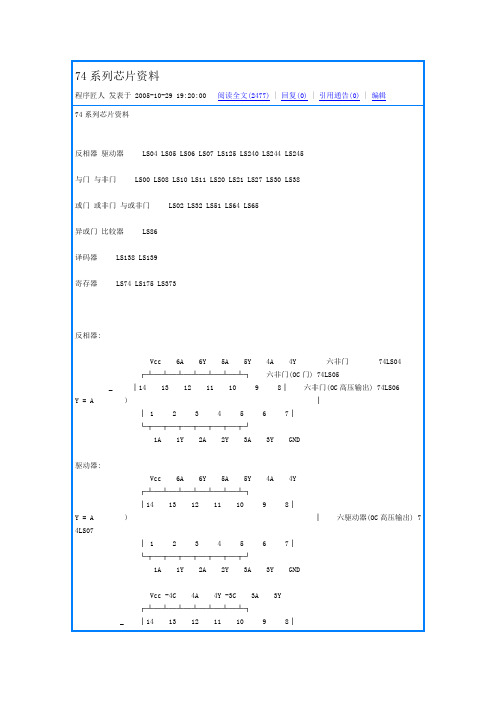
74系列芯片资料程序匠人发表于 2005-10-29 19:20:00 阅读全文(2477) | 回复(0) | 引用通告(0) | 编辑74系列芯片资料反相器驱动器 LS04 LS05 LS06 LS07 LS125 LS240 LS244 LS245与门与非门 LS00 LS08 LS10 LS11 LS20 LS21 LS27 LS30 LS38或门或非门与或非门 LS02 LS32 LS51 LS64 LS65异或门比较器 LS86译码器 LS138 LS139寄存器 LS74 LS175 LS373反相器:Vcc 6A 6Y 5A 5Y 4A 4Y 六非门 74LS04┌┴─┴─┴─┴─┴─┴─┴┐六非门(OC门) 74LS05_ │14 13 12 11 10 9 8│六非门(OC高压输出) 74LS06Y = A )││ 1 2 3 4 5 6 7│└┬─┬─┬─┬─┬─┬─┬┘1A 1Y 2A 2Y 3A 3Y GND驱动器:Vcc 6A 6Y 5A 5Y 4A 4Y┌┴─┴─┴─┴─┴─┴─┴┐│14 13 12 11 10 9 8│Y = A )│六驱动器(OC高压输出) 74LS07│ 1 2 3 4 5 6 7│└┬─┬─┬─┬─┬─┬─┬┘1A 1Y 2A 2Y 3A 3Y GNDVcc -4C 4A 4Y -3C 3A 3Y┌┴─┴─┴─┴─┴─┴─┴┐_ │14 13 12 11 10 9 8│Y =A+C )│四总线三态门 74LS125│ 1 2 3 4 5 6 7│└┬─┬─┬─┬─┬─┬─┬┘-1C 1A 1Y -2C 2A 2Y GNDVcc -G B1 B2 B3 B4 B8 B6 B7 B8┌┴─┴─┴─┴─┴─┴─┴─┴─┴─┴┐ 8位总线驱动器 74LS245 │20 19 18 17 16 15 14 13 12 11│)│ DIR=1 A=>B│ 1 2 3 4 5 6 7 8 9 10│ DIR=0 B=>A└┬─┬─┬─┬─┬─┬─┬─┬─┬─┬┘DIR A1 A2 A3 A4 A5 A6 A7 A8 GND页首非门,驱动器与门,与非门或门,或非门异或门,比较器译码器寄存器正逻辑与门,与非门:Vcc 4B 4A 4Y 3B 3A 3Y┌┴─┴─┴─┴─┴─┴─┴┐│14 13 12 11 10 9 8│Y = AB )│ 2输入四正与门 74LS08 │ 1 2 3 4 5 6 7│└┬─┬─┬─┬─┬─┬─┬┘1A 1B 1Y 2A 2B 2Y GNDVcc 4B 4A 4Y 3B 3A 3Y┌┴─┴─┴─┴─┴─┴─┴┐__ │14 13 12 11 10 9 8│Y = AB )│ 2输入四正与非门 74LS00 │ 1 2 3 4 5 6 7│└┬─┬─┬─┬─┬─┬─┬┘1A 1B 1Y 2A 2B 2Y GNDVcc 1C 1Y 3C 3B 3A 3Y┌┴─┴─┴─┴─┴─┴─┴┐___ │14 13 12 11 10 9 8│Y = ABC )│ 3输入三正与非门 74LS10 │ 1 2 3 4 5 6 7│└┬─┬─┬─┬─┬─┬─┬┘1A 1B 2A 2B 2C 2Y GNDVcc H G Y┌┴─┴─┴─┴─┴─┴─┴┐│14 13 12 11 10 9 8│)│ 8输入与非门 74LS30│ 1 2 3 4 5 6 7│ ________└┬─┬─┬─┬─┬─┬─┬┘ Y = ABCDEFGHA B C D E F GND页首非门,驱动器与门,与非门或门,或非门异或门,比较器译码器寄存器正逻辑或门,或非门:Vcc 4B 4A 4Y 3B 3A 3Y┌┴─┴─┴─┴─┴─┴─┴┐ 2输入四或门 74LS32│14 13 12 11 10 9 8│)│ Y = A+B│ 1 2 3 4 5 6 7│└┬─┬─┬─┬─┬─┬─┬┘1A 1B 1Y 2A 2B 2Y GNDVcc 4Y 4B 4A 3Y 3B 3A┌┴─┴─┴─┴─┴─┴─┴┐ 2输入四或非门 74LS02│14 13 12 11 10 9 8│ ___)│ Y = A+B│ 1 2 3 4 5 6 7│└┬─┬─┬─┬─┬─┬─┬┘1Y 1A 1B 2Y 2A 2B GNDVcc 2Y 2B 2A 2D 2E 1F┌┴─┴─┴─┴─┴─┴─┴┐双与或非门 74S51│14 13 12 11 10 9 8│ _____)│ 2Y = AB+DE│ 1 2 3 4 5 6 7│ _______└┬─┬─┬─┬─┬─┬─┬┘ 1Y = ABC+DEF1Y 1A 1B 1C 1D 1E GNDVcc D C B K J Y┌┴─┴─┴─┴─┴─┴─┴┐ 4-2-3-2与或非门 74S64 74S65(OC门) │14 13 12 11 10 9 8│ ______________)│ Y = ABCD+EF+GHI+JK│ 1 2 3 4 5 6 7│└┬─┬─┬─┬─┬─┬─┬┘A E F G H I GND页首非门,驱动器与门,与非门或门,或非门异或门,比较器译码器寄存器2输入四异或门 74LS86Vcc 4B 4A 4Y 3Y 3B 3A┌┴─┴─┴─┴─┴─┴─┴┐│14 13 12 11 10 9 8│)│ _ _│ 1 2 3 4 5 6 7│ Y=AB+AB└┬─┬─┬─┬─┬─┬─┬┘1A 1B 1Y 2Y 2A 2B GND8*2输入比较器 74LS688_Vcc Y B8 A8 B7 A7 B6 A6 B5 A5┌┴─┴─┴─┴─┴─┴─┴─┴─┴─┴┐ 8*2输入比较器 74LS688│20 19 18 17 16 15 14 13 12 11│)││ 1 2 3 4 5 6 7 8 9 10│└┬─┬─┬─┬─┬─┬─┬─┬─┬─┬┘CE A1 B1 A2 B2 A3 B3 A4 B4 GND_Y=A1⊙B1+A2⊙B2+A3⊙B3+A4⊙B4+A5⊙B5+A6⊙B6+A7⊙B7+A8⊙B8页首非门,驱动器与门,与非门或门,或非门异或门,比较器译码器寄存器3-8译码器 74LS138Vcc -Y0 -Y1 -Y2 -Y3 -Y4 -Y5 -Y6 __ _ _ _ __ _ _ __ _ _ __ _ ┌┴─┴─┴─┴─┴─┴─┴─┴┐ Y0=A B C Y1=A B B Y2=A B C Y3=A B C │16 15 14 13 12 11 10 9 │)│ __ _ _ __ _ __ _ __│ 1 2 3 4 5 6 7 8│ Y4=A B C Y5=A B C Y6=A B C Y7=A B C └┬─┬─┬─┬─┬─┬─┬─┬┘A B C -CS0 -CS1 CS2 -Y7 GND双2-4译码器 74LS139Vcc -2G 2A 2B -Y0 -Y1 -Y2 -Y3 __ __ __ __ __ __ __ __┌┴─┴─┴─┴─┴─┴─┴─┴┐ Y0=2A 2B Y1=2A 2B Y2=2A 2B Y3=2A 2B │16 15 14 13 12 11 10 9 │)│ __ __ __ __ __ __ __ __│ 1 2 3 4 5 6 7 8│ Y0=1A 1B Y1=1A 1B Y2=1A 1B Y3=1A 1B └┬─┬─┬─┬─┬─┬─┬─┬┘-1G 1A 1B -Y0 -Y1 -Y2 -Y3 GND8*2输入比较器 74LS688_Vcc Y B8 A8 B7 A7 B6 A6 B5 A5┌┴─┴─┴─┴─┴─┴─┴─┴─┴─┴┐ 8*2输入比较器 74LS688│20 19 18 17 16 15 14 13 12 11│)││ 1 2 3 4 5 6 7 8 9 10│└┬─┬─┬─┬─┬─┬─┬─┬─┬─┬┘CE A1 B1 A2 B2 A3 B3 A4 B4 GND_Y=A1⊙B1+A2⊙B2+A3⊙B3+A4⊙B4+A5⊙B5+A6⊙B6+A7⊙B7+A8⊙B8寄存器:Vcc 2CR 2D 2Ck 2St 2Q -2Q┌┴─┴─┴─┴─┴─┴─┴┐双D触发器 74LS74│14 13 12 11 10 9 8 │)││ 1 2 3 4 5 6 7│└┬─┬─┬─┬─┬─┬─┬┘1Cr 1D 1Ck 1St 1Q -1Q GNDVcc 8Q 8D 7D 7Q 6Q 6D 5D 5Q ALE┌┴─┴─┴─┴─┴─┴─┴─┴─┴─┴┐ 8位锁存器 74LS373│20 19 18 17 16 15 14 13 12 11│)││ 1 2 3 4 5 6 7 8 9 10│└┬─┬─┬─┬─┬─┬─┬─┬─┬─┬┘-OE 1Q 1D 2D 2Q 3Q 3D 4D 4Q GND型号器件名称厂牌[数据表]SN7400四2输入端与非门 TI[DATA]SN7401四2输入端与非门(OC) SN7402四2输入端或非门 TI[DATA]SN7403四2输入端与非门(OC)TI[DATA]SN7404六反相器 TI[DATA]SN7405六反相器(OC)TI[DATA]SN7406六高压输出反相器 (OC,30V)TI[DATA]SN7407六高压输出缓冲,驱动器(OC,30V)TI[DATA]SN7408四2输入端与门 TI[DATA]SN7409四2输入端与门(OC)TI[DATA]SN7410三3输入端与非门 TI[DATA]SN7412三3输入端与非门(OC)TI[DATA]SN7413双4输入端与非门 TI[DATA]SN7414六反相器TI[DATA]SN7416六高压输出反相缓冲/驱动器 I[DATA]SN7417六高压输出缓冲/驱动器(OC,15V)TI[DATA]SN7420双4输入端与非门 TI[DATA]SN7422双4输入端与非门(OC)TI[DATA]SN7423可扩展双4输入端或非门 TI[DATA]SN7425双4输入端或非门TI[DATA]SN7426四2输入端高压输出与非缓冲器 [DATA]SN7427三3输入端或非门TI[DATA]SN7428四2输入端或非缓冲器 I[DATA]SN74308输入端与非门TI[DATA]SN7432四2输入端或门。
- 1、下载文档前请自行甄别文档内容的完整性,平台不提供额外的编辑、内容补充、找答案等附加服务。
- 2、"仅部分预览"的文档,不可在线预览部分如存在完整性等问题,可反馈申请退款(可完整预览的文档不适用该条件!)。
- 3、如文档侵犯您的权益,请联系客服反馈,我们会尽快为您处理(人工客服工作时间:9:00-18:30)。
© 2005 Fairchild Semiconductor Corporation DS500644September 2001Revised February 200574ALVC08 Low Voltage Quad 2-Input AND Gate with 3.6V Tolerant Inputs and Outputs74ALVC08Low Voltage Quad 2-Input AND Gate with 3.6V Tolerant Inputs and OutputsGeneral DescriptionThe ALVC08 contains four 2-input AND gates. This product is designed for low voltage (1.65V to 3.6V) V CC applica-tions with I/O compatibility up to 3.6VThe ALVC08 is fabricated with an advanced CMOS tech-nology to achieve high-speed operation while maintaining low CMOS power dissipation.Featuress 1.65V to 3.6V V CC supply operation s 3.6V tolerant inputs and outputs s t PD2.9 ns max for3.0V to 3.6V V CC 3.2 ns max for 2.3V to 2.7V V CC 5.3 ns max for 1.65V to 1.95V V CCs Power-off high impedance inputs and outputs s Uses patented Quiet Series ¥ noise/EMI reduction circuitry s Latchup conforms to JEDEC JED78s ESD performance:Human body model ! 2000V Machine model ! 250VOrdering Code:Devices also available in T ape and Reel. Specify by appending the suffix letter “X” to the ordering code.Logic SymbolIEEE/IECConnection DiagramPin DescriptionsQuiet Series ¥ is a trademark of Fairchild Semiconductor Corporation.Order Number Package NumberPackage Description74ALVC08M M14A 14-Lead Small Outline Integrated Circuit (SOIC), JEDEC MS-012, 0.150" Narrow 74ALVC08MTCMTC1414-Lead Thin Shrink Small Outline Package (TSSOP), JEDEC MO-153, 4.4mm WidePin Names Description A n , B n Inputs O nOutputs 274A L V C 08Absolute Maximum Ratings (Note 1)Recommended Operating Conditions (Note 3)Note 1: The Absolute Maximum Ratings are those values beyond which the safety of the device cannot be guaranteed. The device should not be operated at these limits. The parametric values defined in the Electrical Characteristics tables are not guaranteed at the Absolute Maximum Rat-ings. The “Recommended Operating Conditions ” table will define the condi-tions for actual device operation.Note 2: I O Absolute Maximum Rating must be observed, limited to 4.6V.Note 3: Floating or unused control inputs must be held HIGH or LOW.DC Electrical CharacteristicsSupply Voltage (V CC ) 0.5V to 4.6V DC Input Voltage (V I ) 0.5V to 4.6V Output Voltage (V O ) (Note 2) 0.5V to V CC 0.5VDC Input Diode Current (I IK ) V I 0V50 mA DC Output Diode Current (I OK )V O 0V50 mA DC Output Source/Sink Current (I OH /I OL )r 50 mA DC V CC or GND Current per Supply Pin (I CC or GND)r 100 mAStorage Temperature Range (T STG )65q C to 150q CPower Supply Operating 1.65V to 3.6VInput Voltage (V I )0V to V CC Output Voltage (V O )0V to V CCFree Air Operating Temperature (T A ) 40q C to 85q CMinimum Input Edge Rate ('t/'V)V IN 0.8V to 2.0V, V CC 3.0V5 ns/VSymbol ParameterConditionsV CC Min MaxUnits(V)V IHHIGH Level Input Voltage1.65 - 1.950.65 x V CCV2.3 - 2.7 1.72.7 -3.62.0V ILLOW Level Input Voltage1.65 - 1.950.35 x V CCV 2.3 - 2.70.72.7 - 3.60.8V OHHIGH Level Output VoltageI OH 100 P A 1.65 - 3.6V CC - 0.2VI OH 4 mA 1.65 1.2I OH 6 mA 2.3 2.0I OH 12 mA2.3 1.72.7 2.23.02.4I OH 24 mA3.02V OLLOW Level Output VoltageI OL 100 P A 1.65 - 3.60.2V I OL 4 mA 1.650.45I OL 6 mA 2.30.4I OL 12 mA 2.30.72.70.4I OL 24 mA3.00.55I I Input Leakage Current 0 d V I d 3.6V3.6r 5.0P A I CC Quiescent Supply Current V I V CC or GND, I O 0 3.640P A 'I CCIncrease in I CC per InputV IH V CC 0.6V3 - 3.6750P A74ALVC08AC Electrical CharacteristicsCapacitanceAC Loading and WaveformsFIGURE 1. AC Test CircuitTABLE 1. Values for Figure 1TABLE 2. Variable Matrix(Input Characteristics: f 1MHz; t r t f 2ns; Z 0 50:)FIGURE 2. Waveform for Inverting and Non-inverting FunctionsSymbolParameterT A 40q C to 85q C, R L 500:UnitsC L 50 pFC L 30 pFV CC 3.3V r 0.3V V CC 2.7V V CC 2.5V r 0.2VV CC 1.8V r 0.15V MinMax MinMax Min Max Min Max t PHL , t PLHPropagation Delay1.22.93.01.03.21.25.3ns Symbol ParameterConditionsT A 25q C Units V CC Typical C IN Input CapacitanceV I 0V or V CC3.34.5pFC PDPower Dissipation Capacitancef 10 MHz, C L 50 pF3.326pF 2.5251.824TEST SWITCH t PLH , t PHLOpenSymbol V CC3.3V r 0.3V2.7V 2.5V r 0.2V 1.8V r 0.15VV mi 1.5V 1.5V V CC /2V CC /2V mo1.5V1.5VV CC /2V CC /2 474A L V C 08Physical Dimensionsinches (millimeters) unless otherwise noted14-Lead Small Outline Integrated Circuit (SOIC), JEDEC MS-012, 0.150" NarrowPackage Number M14A574ALVC08 Low Voltage Quad 2-Input AND Gate with 3.6V Tolerant Inputs and OutputsPhysical Dimensions inches (millimeters) unless otherwise noted (Continued)14-Lead Thin Shrink Small Outline Package (TSSOP), JEDEC MO-153, 4.4mm WidePackage Number MTC14Fairchild does not assume any responsibility for use of any circuitry described, no circuit patent licenses are implied and Fairchild reserves the right at any time without notice to change said circuitry and specifications.LIFE SUPPORT POLICYFAIRCHILD ’S PRODUCTS ARE NOT AUTHORIZED FOR USE AS CRITICAL COMPONENTS IN LIFE SUPPORT DEVICES OR SYSTEMS WITHOUT THE EXPRESS WRITTEN APPROVAL OF THE PRESIDENT OF FAIRCHILD SEMICONDUCTOR CORPORATION. As used herein:1.Life support devices or systems are devices or systems which, (a) are intended for surgical implant into the body, or (b) support or sustain life, and (c) whose failure to perform when properly used in accordance with instructions for use provided in the labeling, can be rea-sonably expected to result in a significant injury to the user.2. A critical component in any component of a life support device or system whose failure to perform can be rea-sonably expected to cause the failure of the life support device or system, or to affect its safety or effectiveness.。