K9K1G08Q0A-GCB0中文资料
K9NBG08U5M-PIB0中文资料

K9XXG08UXMINFORMATION IN THIS DOCUMENT IS PROVIDED IN RELATION TO SAMSUNG PRODUCTS, AND IS SUBJECT TO CHANGE WITHOUT NOTICE.NOTHING IN THIS DOCUMENT SHALL BE CONSTRUED AS GRANTING ANY LICENSE, EXPRESS OR IMPLIED, BY ESTOPPEL OR OTHERWISE,TO ANY INTELLECTUAL PROPERTY RIGHTS IN SAMSUNG PRODUCTS OR TECHNOLOGY. ALL INFORMATION IN THIS DOCUMENT IS PROVIDEDON AS "AS IS" BASIS WITHOUT GUARANTEE OR WARRANTY OF ANY KIND.1. For updates or additional information about Samsung products, contact your nearest Samsung office.2. Samsung products are not intended for use in life support, critical care, medical, safety equipment, or similar applications where Product failure could result in loss of life or personal or physical harm, or any military or defense application, or any governmental procurement to which special terms or provisions may apply.* Samsung Electronics reserves the right to change products or specification without notice.Document Title1G x 8 Bit / 2G x 8 Bit / 4G x 8 Bit NAND Flash Memory Revision HistoryThe attached data sheets are prepared and approved by SAMSUNG Electronics. SAMSUNG Electronics CO., LTD. reserve the rightto change the specifications. SAMSUNG Electronics will evaluate and reply to your requests and questions about device. If you have any questions, please contact the SAMSUNG branch office near your office.Revision No0.00.10.20.31.0RemarkAdvance Advance Preliminary Preliminary FinalHistory1. Initial issue1. Technical note is changed 1. Icc value is changedDraft DateMar. 1st. 2005Apr. 1st. 2005May 3rd. 2005Sep. 26th. 2005Nov. 4th 2005GENERAL DESCRIPTIONFEATURES• Voltage Supply - 2.70V ~ 3.60V • Organization- Memory Cell Array : (1G + 32M) x 8bit - Data Register : (2K + 64) x 8bit • Automatic Program and Erase - Page Program : (2K + 64)Byte - Block Erase : (128K + 4K)Byte • Page Read Operation- Page Size : (2K + 64)Byte - Random Read : 20µs(Max.) - Serial Access : 25ns(Min.) * K9NBG08U5M : 50ns(Min.) • Fast Write Cycle Time- Page Program time : 200µs(Typ.) - Block Erase Time : 1.5ms(Typ.)1G x 8 Bit / 2G x 8 Bit / 4G x 8 Bit NAND Flash Memory• Command/Address/Data Multiplexed I/O Port • Hardware Data Protection- Program/Erase Lockout During Power Transitions • Reliable CMOS Floating-Gate Technology- Endurance : 100K Program/Erase Cycles (with 1bit/512Byte ECC) - Data Retention : 10 Years • Command Driven Operation• Intelligent Copy-Back with internal 1bit/528Byte EDC • Unique ID for Copyright Protection • Package :- K9K8G08U0M-YCB0/YIB048 - Pin TSOP I (12 x 20 / 0.5 mm pitch)- K9K8G08U0M-PCB0/PIB0 : Pb-FREE PACKAGE 48 - Pin TSOP I (12 x 20 / 0.5 mm pitch) - K9WAG08U1M-YCB0/YIB048 - Pin TSOP I (12 x 20 / 0.5 mm pitch)- K9WAG08U1M-PCB0/PIB0 : Pb-FREE PACKAGE 48 - Pin TSOP I (12 x 20 / 0.5 mm pitch) - K9WAG08U1M-ICB0/IIB052 - Pin TLGA (12 x 17 / 1.0 mm pitch)- K9NBG08U5M-PCB0/PIB0 : Pb-FREE PACKAGE 48 - Pin TSOP I (12 x 20 / 0.5 mm pitch)Offered in 1G x 8bit, the K9K8G08U0M is a 8G-bit NAND Flash Memory with spare 256M-bit. Its NAND cell provides the most cost-effective solution for the solid state application market. A program operation can be performed in typical 200µs on the (2K+64)Byte page and an erase operation can be performed in typical 1.5ms on a (128K+4K)Byte block. Data in the data register can be read out at 25ns(K9NBG08U5M:50ns) cycle time per Byte. The I/O pins serve as the ports for address and data input/output as well as com-mand input. The on-chip write controller automates all program and erase functions including pulse repetition, where required, and internal verification and margining of data. Even the write-intensive systems can take advantage of the K9K8G08U0M ′s extended reliability of 100K program/erase cycles by providing ECC(Error Correcting Code) with real time mapping-out algorithm. The K9K8G08U0M is an optimum solution for large nonvolatile storage applications such as solid state file storage and other portable applications requiring non-volatility.An ultra high density solution having two 8Gb stacked with two chip selects is also available in standard TSOPI package and another ultra high density solution having two 16Gb TSOPI package stacked with four chip selects is also available in TSOPI-DSP .PRODUCT LISTPart Number Vcc RangeOrganizationPKG Type K9K8G08U0M-Y ,P 2.70 ~ 3.60VX8TSOP1K9WA G08U1M-Y ,P K9WA G08U1M-I 52TLGA K9NBG08U5M-PTSOP1-DSP1.001.001.001.002.007 6 5 4 3 2 11.001.001.0012.00±0.10#A117.00±0.1017.00±0.10BA12.00±0.10(Datum B)(Datum A)12.0010.002.502.502.000.501.30A B C DEF GHJ K L M N12-∅1.00±0.0541-∅0.70±0.05Side View1.0(M a x .)0.10 C17.00±0.10Top ViewBottom ViewABC D EF G H J KL M N7654321K9WAG08U1M - ICB0 / IIB052-TLGA (measured in millimeters)NCNCNCNCNCNCNCNCNC NCNCNCNCNCNC NCVccVcc VssVssVss /RE1/RE2/CE1/CE2CLE1CLE2ALE1ALE2/WE1/WE2/WP1/WP2R/B1R/B2VssIO0-1IO0-2IO1-1IO1-2IO2-1IO3-1IO2-2IO3-2IO4-1IO4-2IO5-1IO5-2IO6-1IO6-2IO7-1IO7-2∅ABC M 0.1∅ABC M 0.1PACKAGE DIMENSIONSPIN DESCRIPTIONNOTE : Connect all V CC and V SS pins of each device to common power supply outputs. Do not leave V CC or V SS disconnected.There are two CE pins (CE 1 & CE 2) in the K9WAG08U1M and four CE pins (CE 1 & CE 2 & CE 3 & CE 4) in the K9NBG08U5M.There are two R/B pins (R/B1 & R/B2) in the K9WAG08U1M and four R/B pins (R/B1 & R/B2 & R/B3 & R/B4) in the K9NBG08U5M.Pin Name Pin FunctionI/O 0 ~ I/O 7DATA INPUTS/OUTPUTSThe I/O pins are used to input command, address and data, and to output data during read operations. The I/O pins float to high-z when the chip is deselected or when the outputs are disabled.CLECOMMAND LATCH ENABLEThe CLE input controls the activating path for commands sent to the command register. When active high, commands are latched into the command register through the I/O ports on the rising edge of the WE signal.ALEADDRESS LATCH ENABLEThe ALE input controls the activating path for address to the internal address registers. Addresses are latched on the rising edge of WE with ALE high.CE / CE1CHIP ENABLEThe CE / CE1 input is the device selection control. When the device is in the Busy state, CE / CE1 high is ignored, and the device does not return to standby mode in program or erase operation.Regarding CE / CE1 control during read operation , refer to ’Page Read’ section of Device operation. CE2CHIP ENABLEThe CE2 input enables the second K9K8G08U0MREREAD ENABLEThe RE input is the serial data-out control, and when active drives the data onto the I/O bus. Data is valid tREA after the falling edge of RE which also increments the internal column address counter by one.WEWRITE ENABLEThe WE input controls writes to the I/O port. Commands, address and data are latched on the rising edge of the WE pulse.WPWRITE PROTECTThe WP pin provides inadvertent program/erase protection during power transitions. The internal high volt-age generator is reset when the WP pin is active low.R/B / R/B1READY/BUSY OUTPUTThe R/B / R/B1 output indicates the status of the device operation. When low, it indicates that a program, erase or random read operation is in process and returns to high state upon completion. It is an open drain output and does not float to high-z condition when the chip is deselected or when outputs are disabled.Vcc POWERV CC is the power supply for device. Vss GROUNDN.CNO CONNECTIONLead is not internally connected.Product IntroductionThe K9K8G08U0M is a 8,448Mbit(8,858,370,048 bit) memory organized as 524,288 rows(pages) by 2,112x8 columns. Spare 64x8 columns are located from column address of 2,048~2,111. A 2,112-byte data register is connected to memory cell arrays accommo-dating data transfer between the I/O buffers and memory during page read and page program operations. The memory array is made up of 32 cells that are serially connected to form a NAND structure. Each of the 32 cells resides in a different page. A block consists of two NAND structured strings. A NAND structure consists of 32 cells. Total 1,081,344 NAND cells reside in a block. The program and read operations are executed on a page basis, while the erase operation is executed on a block basis. The memory array con-sists of 8,192 separately erasable 128K-byte blocks. It indicates that the bit by bit erase operation is prohibited on the K9K8G08U0M. The K9K8G08U0M has addresses multiplexed into 8 I/Os. This scheme dramatically reduces pin counts and allows system upgrades to future densities by maintaining consistency in system board design. Command, address and data are all written through I/O's by bringing WE to low while CE is low. Those are latched on the rising edge of WE. Command Latch Enable(CLE) and Address Latch Enable(ALE) are used to multiplex command and address respectively, via the I/O pins. Some commands require one bus cycle. For example, Reset Command, Status Read Command, etc require just one cycle bus. Some other commands, like page read and block erase and page program, require two cycles: one cycle for setup and the other cycle for execution. The 1056M byte physical space requires 31 addresses, thereby requiring five cycles for addressing : 2 cycles of column address, 3 cycles of row address, in that order. Page Read and Page Program need the same five address cycles following the required command input. In Block Erase oper-ation, however, only the three row address cycles are used. Device operations are selected by writing specific commands into the command register. Table 1 defines the specific commands of the K9K8G08U0M.In addition to the enhanced architecture and interface, the device incorporates copy-back program feature from one page to another page without need for transporting the data to and from the external buffer memory. Since the time-consuming serial access and data-input cycles are removed, system performance for solid-state disk application is significantly increased.The K9WAG08U1M is composed of two K9K8G08U0M chips which are selected separately by each CE1 and CE2 and the K9NBG08U5M is composed of four K9K8G08U0M chips which are selected seperately by each CE1, CE2, CE3 and CE4. Therefore, in terms of each CE, the basic operations of K9WAG08U0M and K9NBG08U5M are same with K9K8G08U0M except some AC/DC charateristics.Table 1. Command SetsFunction1st Cycle2nd Cycle Acceptable Command during Busy Read 00h30hRead for Copy Back00h35hRead ID90h-Reset FFh-OPage Program80h10hTwo-Plane Page Program(4)80h---11h81h---10hCopy-Back Program85h10hTwo-Plane Copy-Back Program(4)85h---11h81h---10hBlock Erase60h D0hTwo-Plane Block Erase60h---60h D0hRandom Data Input(1)85h-Random Data Output(1)05h E0hRead Status70h ORead EDC Status(2)7Bh OChip1 Status(3)F1h OChip2 Status(3)F2h ONOTE : 1. Random Data Input/Output can be executed in a page.2. Read EDC Status is only available on Copy Back operation.3. Interleave-operation between two chips is allowed.It’s prohibited to use F1h and F2h commands for other operations except interleave-operation.4.Any command between 11h and 81h is prohibited except 70h, F1h, F2h and FFh .Caution : Any undefined command inputs are prohibited except for above command set of Table 1.DC AND OPERATING CHARACTERISTICS (Recommended operating conditions otherwise noted.)NOTE : 1. V IL can undershoot to -0.4V and V IH can overshoot to V CC +0.4V for durations of 20 ns or less. 2. Typical value is measured at Vcc=3.3V, T A =25°C. Not 100% tested.3. The typical value of the K9WAG08U1M’s I SB 2 is 40µA and the maximum value is 200µA.4. The typical value of the K9NBG08U5M’s I SB 2 is 80µA and the maximum value is 400µA.5. The maximum value of K9WAG08U1M-Y ,P’s I LI and I LO is ±40µA , the maximum value of K9WAG08U1M-I’s I LI and I LO is ±20µA .6. The maximum value of K9NBG08U5M’s I LI and I LO is ±80µA.ParameterSymbol Test ConditionsMinTypMaxUnitOperating CurrentPage Read withSerial Access I CC 1tRC=25ns (K9NBG08U5M: 50ns)CE=V IL, I OUT =0mA-2535mAProgramI CC 2-EraseI CC 3-Stand-by Current(TTL)I SB 1CE=V IH , WP=0V/V CC --1Stand-by Current(CMOS)I SB 2CE=V CC -0.2, WP=0V/V CC -20100µAInput Leakage Current I LI V IN =0 to Vcc(max)--±20Output Leakage Current I LO V OUT =0 to Vcc(max)--±20Input High VoltageV IH (1)-0.8xVcc -Vcc+0.3V Input Low Voltage, All inputs V IL (1)--0.3-0.2xVccOutput High Voltage Level V OH I OH =-400µA 2.4--Output Low Voltage Level V OL I OL =2.1mA --0.4Output Low Current(R/B)I OL (R/B)V OL =0.4V810-mA RECOMMENDED OPERATING CONDITIONS(Voltage reference to GND, K9XXG08UXM-XCB0 :T A =0 to 70°C, K9XXG08UXM-XIB0:T A =-40 to 85°C)ParameterSymbol Min Typ.Max Unit Supply Voltage V CC 2.7 3.3 3.6V Supply VoltageV SSVABSOLUTE MAXIMUM RATINGSNOTE :1. Minimum DC voltage is -0.6V on input/output pins. During transitions, this level may undershoot to -2.0V for periods <30ns. Maximum DC voltage on input/output pins is V CC +0.3V which, during transitions, may overshoot to V CC +2.0V for periods <20ns.2. Permanent device damage may occur if ABSOLUTE MAXIMUM RATINGS are exceeded. Functional operation should be restricted to the conditions as detailed in the operational sections of this data sheet. Exposure to absolute maximum rating conditions for extended periods may affect reliability.ParameterSymbol Rating Unit Voltage on any pin relative to VSSV CC -0.6 to +4.6VV IN -0.6 to +4.6V I/O-0.6 to Vcc+0.3 (<4.6V)Temperature Under Bias K9XXG08UXM-XCB0T BIAS -10 to +125°C K9XXG08UXM-XIB0-40 to +125Storage Temperature K9XXG08UXM-XCB0T STG-65 to +150°CK9XXG08UXM-XIB0Short Circuit CurrentI OS5mACAPACITANCE (T A =25°C, V CC =3.3V, f=1.0MHz)NOTE : Capacitance is periodically sampled and not 100% tested. K9WAG08U1M-IXB0’s capacitance(I/O, Input) is 20pF.ItemSymbol Test Condition Min MaxUnit K9K8G08U0MK9WAG08U1M*K9NBG08U5MInput/Output Capacitance C I/O V IL =0V -204080pF Input CapacitanceC INV IN =0V-204080pFVALID BLOCKNOTE :1. The device may include initial invalid blocks when first shipped. Additional invalid blocks may develop while being used. The number of valid blocks is presented with both cases of invalid blocks considered. Invalid blocks are defined as blocks that contain one or more bad bits. Do not erase or pro-gram factory-marked bad blocks. Refer to the attached technical notes for appropriate management of invalid blocks.2. The 1st block, which is placed on 00h block address, is guaranteed to be a valid block up to 1K program/erase cycles with 1bit/512Byte ECC.3. The number of valid block is on the basis of single plane operations, and this may be decreased with two plane operations.* : Each K9K8G08U0M chip in the K9WAG08U1M and K9NBG08U5M has Maximun 160 invalid blocks.Parameter Symbol Min Typ.Max Unit K9K8G08U0M N VB 8,032-8,192Blocks K9WAG08U1M N VB 16,064*-16,384*BlocksK9NBG08U5MN VB32,128*32,768*AC TEST CONDITION(K9XXG08UXM-XCB0: T A =0 to 70°C, K9XXG08UXM-XIB0:T A =-40 to 85°C ,K9XXG08UXM: Vcc=2.7V~3.6V unless otherwise noted)ParameterK9XXG08UXM Input Pulse Levels 0V to Vcc Input Rise and Fall Times 5ns Input and Output Timing Levels Vcc/2Output Load1 TTL GATE and CL=50pF (K9K8G08U0M-Y ,P/K9WAG08U1M-I) 1 TTL GATE and CL=30pF (K9WAG08U1M-Y ,P) 1 TTL GATE and CL=30pF (K9NBG08U5M-P)MODE SELECTIONNOTE : 1. X can be V IL or V IH.2. WP should be biased to CMOS high or CMOS low for standby.CLE ALE CE WERE WP ModeH L L H X Read Mode Command Input L H L H X Address Input(5clock)H L L H H Write Mode Command Input L H L H H Address Input(5clock)L L L HH Data Input L L L H X Data Output X X X X H X During Read(Busy)X X X X X H During Program(Busy)X X X X X H During Erase(Busy)X X (1)X X X L Write Protect XXHXX0V/V CC (2)Stand-byAC Timing Characteristics for Command / Address / Data InputNOTES : 1. The transition of the corresponding control pins must occur only once while WE is held low 2. tADL is the time from the WE rising edge of final address cycle to the WE rising edge of first data cycleParameterSymbol MinMaxUnitK9NBG08U5MK9K8G08U0M K9NBG08U5MK9K8G08U0M K9WAG08U1MK9WAG08U1MCLE Setup Time t CLS (1)2512--ns CLE Hold Time t CLH 105--ns CE Setup Time t CS (1)3520--ns CE Hold Time t CH 105--ns WE Pulse Width t WP 2512--ns ALE Setup Time t ALS (1)2512--ns ALE Hold Time t ALH 105--ns Data Setup Time t DS (1)2012--ns Data Hold Time t DH 105--ns Write Cycle Time t WC 4525--ns WE High Hold Timet WH 1510--ns Address to Data Loading Timet ADL (2)7070--ns Program / Erase CharacteristicsNOTE1. Typical value is measured at Vcc=3.3V, T A =25°C. Not 100% tested.2. Typical program time is defined as the time within which more than 50% of the whole pages are programmed at3.3V Vcc and 25°C temperature .ParameterSymbol Min Typ Max Unit Program Time t PROG -200700µs Dummy Busy Time for Two-Plane Page Program t DBSY -0.51µs Number of Partial Program Cycles Nop --4cycles Block Erase Timet BERS- 1.52msAC Characteristics for OperationNOTE : 1. If reset command(FFh) is written at Ready state, the device goes into Busy for maximum 5µs.ParameterSymbol MinMaxUnitK9NBG08U5MK9K8G08U0M K9NBG08U5MK9K8G08U0M K9WAG08U1K9WAG08U1Data Transfer from Cell to Register t R -2020µs ALE to RE Delay t AR 1010-ns CLE to RE Delay t CLR 1010-ns Ready to RE Low t RR 2020-ns RE Pulse Width t RP 2512-ns WE High to Busy t WB --100100ns Read Cycle Time t RC 5025--ns RE Access Time t REA --3020ns CE Access Time t CEA --4525ns RE High to Output Hi-Z t RHZ --100100ns CE High to Output Hi-Z t CHZ --3030ns RE High to Output hold t RHOH 1515--ns RE Low to Output hold t RLOH -5--ns CE High to Output hold t COH 1515--ns RE High Hold Time t REH 1510--ns Output Hi-Z to RE Low t IR 00--ns RE High to WE Low t RHW 100100--ns WE High to RE Lowt WHR 6060--ns Device Resetting Time(Read/Program/Erase)t RST--5/10/500(1)5/10/500(1)µsNAND Flash Technical NotesIdentifying Initial Invalid Block(s)Initial Invalid Block(s)Initial invalid blocks are defined as blocks that contain one or more initial invalid bits whose reliability is not guaranteed by Samsung.The information regarding the initial invalid block(s) is called the initial invalid block information. Devices with initial invalid block(s)have the same quality level as devices with all valid blocks and have the same AC and DC characteristics. An initial invalid block(s)does not affect the performance of valid block(s) because it is isolated from the bit line and the common source line by a select tran-sistor. The system design must be able to mask out the initial invalid block(s) via address mapping. The 1st block, which is placed on 00h block address, is guaranteed to be a valid block up to 1K program/erase cycles with 1bit /512Byte ECC.All device locations are erased(FFh) except locations where the initial invalid block(s) information is written prior to shipping. The ini-tial invalid block(s) status is defined by the 1st byte in the spare area. Samsung makes sure that either the 1st or 2nd page of every initial invalid block has non-FFh data at the column address of 2048. Since the initial invalid block information is also erasable in most cases, it is impossible to recover the information once it has been erased. Therefore, the system must be able to recognize the initial invalid block(s) based on the original initial invalid block information and create the initial invalid block table via the following suggested flow chart(Figure 3). Any intentional erasure of the original initial invalid block information is prohibited.*Check "FFh" at the column address 2048 Figure 3. Flow chart to create initial invalid block table.StartSet Block Address = 0Check "FFh"Increment Block AddressLast Block ?EndNoYesYesCreate (or update)NoInitialof the 1st and 2nd page in the blockInvalid Block(s) TableNAND Flash Technical Notes (Continued)Program Flow ChartStartI/O 6 = 1 ?I/O 0 = 0 ?No*Write 80hWrite AddressWrite DataWrite 10hRead Status RegisterProgram Completedor R/B = 1 ?Program ErrorYesNoYes: If program operation results in an error, map out the block including the page in error and copy thetarget data to another block.*Error in write or read operationWithin its life time, additional invalid blocks may develop with NAND Flash memory. Refer to the qualification report for the actual data.The following possible failure modes should be considered to implement a highly reliable system. In the case of status read fail-ure after erase or program, block replacement should be done. Because program status fail during a page program does not affect the data of the other pages in the same block, block replacement can be executed with a page-sized buffer by finding an erased empty block and reprogramming the current target data and copying the rest of the replaced block. In case of Read, ECC must be employed. To improve the efficiency of memory space, it is recommended that the read or verification failure due to single bit error be reclaimed by ECC without any block replacement. The said additional block failure rate does not include those reclaimed blocks.Failure ModeDetection and Countermeasure sequenceWrite Erase Failure Status Read after Erase --> Block Replacement Program Failure Status Read after Program --> Block Replacement ReadSingle Bit FailureVerify ECC -> ECC CorrectionECC: Error Correcting Code --> Hamming Code etc. Example) 1bit correction & 2bit detectionNAND Flash Technical Notes (Continued)Copy-Back Operation with EDC & Sector Definition for EDCGenerally, copy-back program is very powerful to move data stored in a page without utilizing any external memory. But, if the source page has one bit error due to charge loss or charge gain, then without EDC, the copy-back program operation could also accumulate bit errors.K9K8G08U0M supports copy-back with EDC to prevent cumulative bit errors. To make EDC valid, the page program operation should be performed on either whole page(2112byte) or sector(528byte). Modifying the data of a sector by Random Data Input before Copy-Back Program must be performed for the whole sector and is allowed only once per each sector. Any partial modification smaller than a sector corrupts the on-chip EDC codes.A 2,112-byte page is composed of 4 sectors of 528-byte and each 528-byte sector is composed of 512-byte main area and 16-byte spare area."A" area 512 Byte(1’st sector)"H" area (4’th sector)Main Field (2,048 Byte)16 Byte"G" area (3’rd sector)16 Byte "F" area (2’nd sector)16 Byte "E" area (1’st sector)16 Byte "B" area 512 Byte(2’nd sector)"C" area 512 Byte(3’rd sector)"D" area 512 Byte(4’th sector)Spare Field (64 Byte)Table 2. Definition of the 528-Byte SectorSector Main Field (Column 0~2,047)Spare Field (Column 2,048~2,111)Area NameColumn AddressArea NameColumn Address 1’st 528-Byte Sector "A"0 ~ 511"E"2,048 ~ 2,0632’nd 528-Byte Sector "B"512 ~ 1,023"F"2,064 ~ 2,0793’rd 528-Byte Sector "C"1,024 ~ 1,535"G"2,080 ~ 2,0954’th 528-Byte Sector"D"1,536 ~ 2,047"H"2,096 ~ 2,111Within a block, the pages must be programmed consecutively from the LSB (least significant bit) page of the block to MSB (most sig-nificant bit) pages of the block. Random page address programming is prohibited.From the LSB page to MSB page DATA IN: Data (1)Data (64)(1)(2)(3)(32)(64)Data register Page 0Page 1Page 2Page 31Page 63Ex.) Random page program (Prohibition)DATA IN: Data (1)Data (64)(2)(32)(3)(1)(64)Data registerPage 0Page 1Page 2Page 31Page 63Addressing for program operation::::Interleave Page ProgramK9K8G08U0M is composed of two K9F4G08U0Ms. K9K8G08U0M provides interleaving operation between two K9F4G08U0Ms. This interleaving page program improves the system throughput almost twice compared to non-interleaving page program.At first, the host issues page program command to one of the K9F4G08U0M chips, say K9F4G08U0M(chip #1). Due to this K9K8G08U0M goes into busy state. During this time, K9F4G08U0M(chip #2) is in ready state. So it can execute the page program command issued by the host.After the execution of page program by K9F4G08U0M(chip #1), it can execute another page program regardless of the K9F4G08U0M(chip #2). Before that the host needs to check the status of K9F4G08U0M(chip #1) by issuing F1h command. Only when the status of K9F4G08U0M(chip #1) becomes ready status, host can issue another page program command. If the K9F4G08U0M(chip #1) is in busy state, the host has to wait for the K9F4G08U0M(chip #1) to get into ready state.Similarly, K9F4G08U0M chip(chip #2) can execute another page program after the completion of the previous program. The host can monitor the status of K9F4G08U0M(chip #2) by issuing F2h command. When the K9F4G08U0M(chip #2) shows ready state, host can issue another page program command to K9F4G08U0M(chip #2).This interleaving algorithm improves the system throughput almost twice. The host can issue page program command to each chip individually. This reduces the time lag for the completion of operation.NOTES : During interleave operations, 70h command is prohibited.R / B (#1)b u s y o f C h i p #1I /O X80h10h C o m m a n d A 30 : L o w A d d & D a t a80h 10h A 30 : H i g h A d d & D a t ab u s y o f C h i p #2i n t e r n a l o n l yR /B (#2)i n t e r n a l o n l yR /BI n t e r l e a v e P a g e P r o g r a m≈≈≈F 1h o r F 2h A B CDa n o t h e r p a g e p r o g r a m o n C h i p #1S t a t e A : C h i p #1 i s e x e c u t i n g a p a g e p r o g r a m o p e r a t i o n a n d c h i p #2 i s i n r e a d y s t a t e . S o t h e h o s t c a n i s s u e a p a g e p r o g r a m c o m m a n d t o c h i p #2.S t a t e B : B o t h c h i p #1 a n d c h i p #2 a r e e x e c u t i n g p a g e p r o g r a m o p e r a t i o n .S t a t e C : P a g e p r o g r a m o n c h i p #1 i s t e r m i n a t e d , b u t p a g e p r o g r a m o n c h i p #2 i s s t i l l o p e r a t i n g . A n d t h e s y s t e m s h o u l d i s s u e F 1h c o m m a n d t o d e t e c t t h e s t a t u s o f c h i p #1. I f c h i p #1 i s r e a d y , s t a t u s I /O 6 i s "1" a n d t h e s y s t e m c a n i s s u e a n o t h e r p a g e p r o g r a m c o m m a n d t o c h i p #1.S t a t e D : C h i p #1 a n d C h i p #2 a r e r e a d y .A c c o r d i n g t o t h e a b o v e p r o c e s s , t h e s y s t e m c a n o p e r a t e p a g e p r o g r a m o n c h i p #1 a n d c h i p #2 a l t e r n a t e l y .S t a t u sO p e r a t i o nS t a t u s C o m m a n d / D a t aF 1hF 2hAC h i p 1 : B u s y , C h i p 2 : R e a d y8x hC x hBC h i p 1 : B u s y , C h i p 2 : B u s y8x h8x hCC h i p 1 : R e a d y , C h i p 2 : B u s yC x h8x hDC h i p 1 : R e a d y , C h i p 2 : R e a d yC x hC x h。
K9F1G08UOM数据手册

m A 5 5 15 15 1 10 10 20 20 1 µA 10 50 10 50
页 编 ICC2 程 擦除 ICC3 ISB1 等待状态电流 (TTL) 等待状态电流 (CMOS) 输入开漏电流 输出开漏电流
ISB2
IL1 IL0
-
-
±10 ±10
-
-
±10 ±10 VCC V +0.3 0.8 -
6. 命令/地址/ 数据复用端口: 7. 硬件数据保护:编程/擦除操作在电源转换时关闭。 8. 可靠的 CMOS 浮置门技术: --保证:100K 编程/ 擦除次数。 --数据保持时间: 10 年。 9. 命令寄存器操作 10. 为高速编程设置的缓冲编程操作。 11. 通电自动读操作。 12. 智能复制拷贝操作。 13.为防盗版而设置的唯一的 ID 保护。 14. 封装。 - K9F1GXXX0M-YCB0/YIB0 48 - Pin TSOP I (12 x 20 / 0.5 mm pitch) - K9F1G08U0M-VCB0/VIB0 48 - Pin WSOP I (12X17X0.7mm)
器件描述
三星 K9F1GXXX0M 提供了 128M*8Bit/64M*16Bit 的存储容量,另外还有 32 M 的空闲存储器,它是采用 NAND 技术的大容量、高可靠的 Flash 存储器。 它对 2112 字节一页(*8device )或者 1056 字(*16device)一页的写操作。典型 时间是 300 微秒。对 128 字节/64K 字一块的擦除时间是 50 纳秒。输出引脚可 以作为数据/地址/命令复用。每一页的数据读出时间也很快,平均每个字节只 需 50 纳秒。片内的写控制器,可以自动执行写操作和擦除功能,包括必要的脉 冲产生器,内部校验和冗余数据。 K9F1G08 提供了实时映像算法的纠错码,写 操作系统可以利用 K9F1G08U0M 扩展的 100K 编程/ 擦除。K9F1G08U0M 为大 容量存储,新型电可擦写的非易失性半导体存储器,提供了最优方案。
K9F2G08U0-存储NFlash

1.0
1.1
1. 1.8V AC timing is changed
2. tRPB/tRCB/tREAB is added for 1.8V device
1.2
1. tCSD is changed.(10ns -> 0ns)
1.3
1. tCS 31ns -> 25ns, tREH 15ns -> 10ns (@ 1.8V)
33
N.C
32
I/O3
31
I/O2
30
I/O1
29
I/O0
28
N.C
27
N.C
26
N.C
25
N.C
PACKAGE DIMENSIONS
48-PIN LEAD/LEAD FREE PLASTIC THIN SMALL OUT-LINE PACKAGE TYPE(I) 48 - TSOP1 - 1220F
17
WE
18
WP
19
N.C
20
N.C
21
N.C
22
N.C
23
N.C
24
48-pin TSOP1 Standard Type 12mm x 20mm
48
N.C
47
N.C
46
N.C
45
N.C
44
I/O7
43
I/O6
42
I/O5
41
I/O4
40
N.C
39
N.C
38
N.C
37
Vcc
36
Vss
35
N.C
34
N.C
Revision History
新型大容量闪存芯片-K9K2GXXU0M.

新型大容量闪存芯片-K9K2GXXU0M文章作者:闫巍李刚林凌文章出处:国外电子元器件摘要:K9K2GXXU0M是三星公司生产的大容量闪存芯片,它的单片容量可高达256M。
文中主要介绍了K9K2GXXU0M的特性、管脚功能和操作指令,重点说明了K9K2GXXU0M闪存的各种工作状态,并给出了它们的工作时序。
关键词:闪存;K9K2GXXU0M;大容量 Flash闪存(FLASH MEMORY闪烁存储器)是一种可以进行电擦写,并在掉电后信息不丢失的存储器,同时该存储器还具有不挥发、功耗低、擦写速度快等特点,因而可广泛应用于外部存储领域,如个人计算机和MP3、数码照相机等。
但随着闪存应用的逐渐广泛,对闪存芯片容量的要求也越来越高,原来32M、64M的单片容量已经不能再满足人们的要求了。
而 K9K2GXXX0M的出现则恰好弥补了这一不足。
K9K2GXXX0M是三星公司开发的目前单片容量最大的闪存芯片,它的单片容量高达256M,同时还提供有8M额外容量。
该闪存芯片是通过与非单元结构来增大容量的。
芯片容量的提高并没有削弱K9K2GXXX0M的功能,它可以在400µs内完成一页2112个字节的编程操作,还可以在2ms内完成128k字节的擦除操作,同时数据区内的数据能以50ns/byte的速度读出。
K9K2GXXU0M大容量闪存芯片的I/O口既可以作为地址的输入端,也可以作为数据的输入/输出端,同时还可以作为指令的输入端。
芯片上的写控制器能自动控制所有编程和擦除操作,包括提供必要的重复脉冲、内部确认和数据空间等。
1 K9K2GXXU0M的性能参数K9K2GXXU0M的主要特点如下:●采用3.3V电源;●芯片内部的存储单元阵列为(256M+8.192M)bit×8bit,数据寄存器和缓冲存储器均为(2k+64)bit×8bit;●具有指令/地址/数据复用的I/O口;●在电源转换过程中,其编程和擦除指令均可暂停;●由于采用可靠的CMOS移动门技术,使得芯片最大可实现100kB编程/擦除循环,该技术可以保证数据保存10年而不丢失。
mapgisk9
mapgisk9Introductionmapgisk9 is a powerful mapping tool that combines the functionalities of GIS (Geographical Information System) and the popular K9 search and rescue strategy. This software application is designed to assist search and rescue teams in efficiently locating missing persons by integrating GIS data with real-time K9 tracking information. The mapgisk9 tool provides a user-friendly interface for displaying and analyzing geographic data while incorporating dynamic K9 tracking updates. This document will provide an overview of the key features and benefits of mapgisk9, as well as a step-by-step guide on how to use the software.Features1. Geographic Information Systemmapgisk9 incorporates a comprehensive GIS system that allows users to view and analyze various geographical data layers. This includes satellite imagery, topographic maps, road networks, and land surface features. The GIS functionality enables search and rescue teams to gain a better understanding of the terrain and environment in which they are operating.2. Real-time K9 TrackingOne of the unique features of mapgisk9 is its ability to track K9 units in real-time. This feature is critical in search andrescue operations as it allows users to monitor the movement and position of the K9 teams on the map. Through GPS and other tracking technologies, mapgisk9 provides up-to-date information on the K9 units, enhancing situational awareness and enabling quick decision-making.3. Search Area Definitionmapgisk9 allows users to define the search area by drawing polygons on the map. This helps in creating a targeted search plan and optimizing the deployment of K9 units. Users can easily drag and resize the polygons to adjust the search area as needed. The defined search area can also be saved for future use or shared with other team members.4. K9 Team Managementmapgisk9 provides a tool to manage and track K9 teams. Users can create and assign individual profiles to K9 units, including details such as the name of the dog, breed, and handler information. This feature helps in organizing the search operation and allows users to monitor K9 team performance. Additionally, users can set up alerts and notifications to keep track of important events related to theK9 teams.5. Data Visualization and Analysismapgisk9 offers a range of data visualization and analysis tools to assist search and rescue teams. Users can overlay multiple data layers on the map to gain insights into the terrain and environment. The software also provides tools for measuring distances, calculating areas, and conducting spatialanalysis. These capabilities aid in better decision-making and resource allocation during search operations.6. Collaborative Workflowmapgisk9 supports collaborative work among team members. Users can share maps, search plans, and K9 team information with other team members in real-time. This promotes effective communication and coordination among team members, leading to improved search and rescue outcomes.User GuideStep 1: InstallationTo begin using mapgisk9, first, download the software from the official website. Follow the installation instructions to set up the software on your computer.Step 2: Data ImportAfter the installation, launch mapgisk9 and import the required GIS data layers. This may include satellite imagery, topographic maps, and other relevant datasets. Ensure that the data is in a compatible format (such as Shapefile or GeoJSON) for import.Step 3: K9 Team SetupCreate individual profiles for the K9 teams that will be participating in the search operation. Enter relevant detailssuch as the dog’s name, breed, and handler information. Assign specific K9 teams to the search operation.Step 4: Search Area DefinitionUsing the drawing tools in the software, define the search area by drawing polygons on the map. Adjust the shape and size of the polygons as necessary.Step 5: Real-time TrackingActivate the real-time tracking feature by connecting the GPS devices carried by the K9 teams. Ensure that the GPS devices are compatible with mapgisk9. This will enable the software to record and display the live movement of the K9 teams on the map.Step 6: Data AnalysisUtilize the various data visualization and analysis tools provided by mapgisk9 to gain insights into the search area. Overlay important data layers, measure distances, calculate areas, and perform spatial analysis to aid in decision-making.Step 7: CollaborationCollaborate with other team members by sharing maps, search plans, and K9 team information. Ensure that everyone has access to the real-time updates and can actively contribute to the search operation.Conclusionmapgisk9 is a powerful tool that integrates GIS capabilities with real-time K9 tracking to enhance search and rescue operations. With its user-friendly interface and comprehensive features, mapgisk9 enables efficient search area definition, precise K9 team tracking, and data analysis for better decision-making. By utilizing mapgisk9, search and rescue teams can improve their operational effectiveness and ultimately increase the chances of finding missing persons.。
MEMORY存储芯片K9F1G08U0B-PCB0中文规格书

Product IntroductionThe K9F1G08U0B is a 1,056Mbit(1,107,296,256 bit) memory organized as 65,536 rows(pages) by 2,112x8 columns. Spare 64x8 col-umns are located from column address of 2,048~2,111. A 2,112-byte data register is connected to memory cell arrays accommodat-ing data transfer between the I/O buffers and memory during page read and page program operations. The memory array is made up of 32 cells that are serially connected to form a NAND structure. Each of the 32 cells resides in a different page. A block consists of two NAND structured strings. A NAND structure consists of 32 cells. Total 1,081,344 NAND cells reside in a block. The program and read operations are executed on a page basis, while the erase operation is executed on a block basis. The memory array consists of 1,024 separately erasable 128K-byte blocks. It indicates that the bit by bit erase operation is prohibited on the K9F1G08U0B.The K9F1G08U0B has addresses multiplexed into 8 I/Os. This scheme dramatically reduces pin counts and allows system upgrades to future densities by maintaining consistency in system board design. Command, address and data are all written through I/O's by bringing WE to low while CE is low. Those are latched on the rising edge of WE. Command Latch Enable(CLE) and Address Latch Enable(ALE) are used to multiplex command and address respectively, via the I/O pins. Some commands require one bus cycle. For example, Reset Command, Status Read Command, etc require just one cycle bus. Some other commands, like page read and block erase and page program, require two cycles: one cycle for setup and the other cycle for execution. The 132M byte physical space requires 28 addresses, thereby requiring four cycles for addressing : 2 cycles of column address, 2 cycles of row address, in that order. Page Read and Page Program need the same four address cycles following the required command input. In Block Erase oper-ation, however, only the two row address cycles are used. Device operations are selected by writing specific commands into the com-mand register. Table 1 defines the specific commands of the K9F1G08U0B.In addition to the enhanced architecture and interface, the device incorporates copy-back program feature from one page to another page without need for transporting the data to and from the external buffer memory. Since the time-consuming serial access and data-input cycles are removed, system performance for solid-state disk application is significantly increased.Table 1. Command SetsNOTE : 1. Random Data Input/Output can be executed in a page.2. Read EDC Status is only available on Copy Back operation.Caution : Any undefined command inputs are prohibited except for above command set of Table 1.Function1st Cycle 2nd CycleAcceptable Command during BusyRead00h 30h Read for Copy Back 00h 35h Read ID 90h -Reset FFh -OPage Program 80h 10h Copy-Back Program 85h 10h Block Erase60h D0h Random Data Input (1)85h -Random Data Output (1)05h E0hRead Status 70h O Read EDC Status (2)7BhODC AND OPERATING CHARACTERISTICS (Recommended operating conditions otherwise noted.)NOTE : 1. V IL can undershoot to -0.4V and V IH can overshoot to V CC +0.4V for durations of 20 ns or less.2. Typical value is measured at Vcc=3.3V, T A =25°C. Not 100% tested.ParameterSymbol Test ConditionsK9F1G08U0B(3.3V)UnitMinTypMaxOperating CurrentPage Read with Serial Access I CC 1tRC=25nsCE=V IL, I OUT =0mA-1530mAProgram I CC 2-EraseI CC 3-Stand-by Current(TTL)I SB 1CE=V IH , WP=0V/V CC --1Stand-by Current(CMOS)I SB 2CE=V CC -0.2, WP=0V/V CC -1050µAInput Leakage Current I LI V IN =0 to Vcc(max)--±10Output Leakage Current I LO V OUT =0 to Vcc(max)--±10Input High VoltageV IH (1)-0.8xVcc -V CC +0.3V Input Low Voltage, All inputs V IL (1)--0.3-0.2xVccOutput High Voltage Level V OH K9F1G08U0A :I OH =-400µA 2.4--Output Low Voltage Level V OLK9F1G08U0A :I OL =2.1mA--0.4Output Low Current(R/B)I OL (R/B)K9F1G08U0A :V OL =0.4V810-mA RECOMMENDED OPERATING CONDITIONS(Voltage reference to GND, K9F1G08U0B-XCB0 :T A =0 to 70°C, K9F1G0808B-XIB0:T A =-40 to 85°C)ParameterSymbol K9F1G08U0B(3.3V)UnitMin Typ.Max Supply Voltage V CC 2.7 3.3 3.6V Supply VoltageV SSV ABSOLUTE MAXIMUM RATINGSNOTE :1. Minimum DC voltage is -0.6V on input/output pins. During transitions, this level may undershoot to -2.0V for periods <30ns. Maximum DC voltage on input/output pins is V CC +0.3V which, during transitions, may overshoot to V CC +2.0V for periods <20ns.2. Permanent device damage may occur if ABSOLUTE MAXIMUM RATINGS are exceeded. Functional operation should be restricted to the conditions as detailed in the operational sections of this data sheet. Exposure to absolute maximum rating conditions for extended periods may affect reliability.ParameterSymbol Rating Unit3.3V Device Voltage on any pin relative to VSSV CC-0.6 to + 4.6VV IN -0.6 to + 4.6V I/O-0.6 to Vcc + 0.3 (< 4.6V)Temperature Under BiasK9XXG08XXB-XCB0T BIAS -10 to +125°C K9XXG08XXB-XIB0-40 to +125Storage Tempera-tureK9XXG08XXB-XCB0T STG-65 to +150°CK9XXG08XXB-XIB0Short Circuit CurrentI OS5mACAPACITANCE (T A =25°C, V CC =3.3V, f=1.0MHz)NOTE : Capacitance is periodically sampled and not 100% tested.ItemSymbol Test ConditionMin Max Unit Input/Output Capacitance C I/O V IL =0V -10pF Input CapacitanceC INV IN =0V-10pFVALID BLOCKNOTE :1. The device may include initial invalid blocks when first shipped. Additional invalid blocks may develop while being used. The number of valid blocks is presented with both cases of invalid blocks considered. Invalid blocks are defined as blocks that contain one or more bad bits. Do not erase or pro-gram factory-marked bad blocks. Refer to the attached technical notes for appropriate management of invalid blocks.2. The 1st block, which is placed on 00h block address, is guaranteed to be a valid block up to 1K program/erase cycles with 1bit/512Byte ECC.ParameterSymbol Min Typ.Max Unit K9F1G08U0BN VB1,004-1,024BlocksMODE SELECTIONNOTE : 1. X can be V IL or V IH.2. WP should be biased to CMOS high or CMOS low for standby.CLE ALE CE WERE WP ModeH L L H X Read Mode Command Input L H L H X Address Input(4clock)H L L H H Write ModeCommand Input L H L H H Address Input(4clock)L L L HH Data Input L L L H XData Output X X X X H X During Read(Busy)X X X X X H During Program(Busy)X X X X X H During Erase(Busy)X X (1)X X X L Write Protect XXHXX0V/V CC (2)Stand-byAC TEST CONDITION(K9F1G08U0B-XCB0 :TA=0 to 70°C, K9F1G08U0B-XIB0:TA=-40 to 85°C, K9F1G08U0B : Vcc=2.7V~3.6V unless otherwise noted)ParameterK9F1G08U0B Input Pulse Levels 0V to Vcc Input Rise and Fall Times 5ns Input and Output Timing Levels Vcc/2Output Load1 TTL GATE and CL=50pF。
大容量NANDFlash在嵌入式系统中的应用

・计算机应用・大容量NAND Flash 在嵌入式系统中的应用汉泽西 吕 飞(西安石油大学电子工程学院 陕西西安)摘 要:文章以主要用于手机领域的Samsung NAND Flash 器件K 9K 1G 08U0B -J I B0为例,对比了NAND 和NOR Flash 的异同,阐述了NAND Flash 的基本结构和使用方法,介绍了大容量NAND Flash 在嵌入式系统中的应用,以及如何在Linux 操作系统中设置对NAND Flash 的支持。
关键词:嵌入式系统;NAND Flash ;K 9K 1G 08U0B -J I B0;Linux中图法分类号:TP333 文献标识码:B 文章编号:100429134(2006)01200622030 引 言在嵌入式市场日益广泛的今天,即将组建的3G网络和多媒体革命将进一步推动移动存储市场的发展。
更多的图片、视频、音乐、3D 游戏、电子地图等在手机、PDA 、MP3、数码相机中的出现,已使得现有设备的存储容量应接不暇。
扩大存储容量,成为各类产品制造商追捧的重点。
在上述各种移动终端设备中,手机占据着核心位置,对存储器的要求也最为严格。
三年前,2MB ~4MB 是手机的存储容量标准,存储器主要使用读取功能,而NOR +SRAM 的结合也是当时唯一的选择。
与此相比,现在的手机中存储了更多的多媒体内容,64MB ~128MB 的存储容量成为标准配置,写性能变得更为重要。
短短3年,在向多媒体平台演变的过程中,手机的存储容量增长了15倍。
继2004年照相功能使手机容量大幅度提升后,音乐功能也将在未来加快存储容量增长的步伐。
所有这些情况都表明了大容量的Nand Flash 会发挥越来越大的作用。
1 NAND 和NO R flash现在的flash memory 主要包括以下两大类:针对程序和数据存储的NOR flash ;针对大容量存储的NAND flash 。
闪存型号容量对照
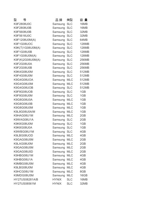
Toshiba
TC58512(A)FT
Toshiba
TC58DVM92A1FT
Toshiba
SLC SLC SLC MLC MLC MLC MLC SLC MLC SLC MLC MLC MLC MLC MLC MLC MLC SLC MLC MLC MLC SLC MLC MLC MLC MLC MLC MLC SLC MLC MLC MLC MLC MLC MLC MLC MLC SLC SLC SLC SLC SLC
HYNIX HYNIX HYNIX HYNIX HYNIX HYNIX HYNIX HYNIX HYNIX HYNIX HYNIX HYNIX HYNIX HYNIX HYNIX HYNIX HYNIX HYNIX HYNIX HYNIX HYNIX HYNIX HYNIX HYNIX HYNIX HYNIX HYNIX HYNIX HYNIX HYNIX HYNIX HYNIX HYNIX HYNIX HYNIX Micron Micron Micron Micron Micron Micron Micron
容量 16MB 16MB 32MB 32MB 64MB 128MB 128MB 128MB 128MB 256MB 256MB 256MB 512MB 512MB 512MB 512MB 512MB 1GB 1GB 1GB 1GB 1GB 1GB 2GB 2GB 1GB 1GB 4GB 4GB 2GB 2GB 2GB 2GB 4GB 4GB 4GB 4GB 8GB 16GB 16MB 32MB
MLC SLC MLC SLC SLC MLC MLC MLC SLC SLC MLC MLC MLC MLC MLC MLC MLC MLC MLC MLC MLC
- 1、下载文档前请自行甄别文档内容的完整性,平台不提供额外的编辑、内容补充、找答案等附加服务。
- 2、"仅部分预览"的文档,不可在线预览部分如存在完整性等问题,可反馈申请退款(可完整预览的文档不适用该条件!)。
- 3、如文档侵犯您的权益,请联系客服反馈,我们会尽快为您处理(人工客服工作时间:9:00-18:30)。
Preliminary
FLASH MEMORY
PACKAGE DIMENSIONS
48-PIN LEAD/LEAD FREE PLASTIC THIN SMALL OUT-LINE PACKAGE TYPE(I) 48 - TSOP1 - 1220F
Unit :mm/Inch
0.10 MAX 0.004 #48 ( 0.25 ) 0.010 12.40 0.488 MAX 0.50 0.0197 #24 #25 1.00±0.05 0.039±0.002 0.25 0.010 TYP 18.40±0.10 0.724±0.004
元器件交易网
K9K1G08Q0A K9K1G16Q0A K9K1G08U0A K9K1G16U0A
Preliminary
FLASH MEMORY
Document Title 128M x 8 Bit / 64M x 16 Bit NAND Flash Memory Revision History
2
元器件交易网
K9K1G08Q0A K9K1G16Q0A K9K1G08U0A K9K1G16U0A
PIN CONFIGURATION (TSOP1)
K9K1G08U0A-YCB0,PCB0/YIB0,PIB0
N.C N.C N.C N.C N.C N.C R/B RE CE N.C N.C Vcc Vss N.C N.C CLE ALE WE WP N.C N.C N.C N.C N.C 1 2 3 4 5 6 7 8 9 10 11 12 13 14 15 16 17 18 19 20 21 22 23 24 48 47 46 45 44 43 42 41 40 39 38 37 36 35 34 33 32 31 30 29 28 27 26 25 N.C N.C N.C N.C I/O7 I/O6 I/O5 I/O4 N.C N.C N.C Vcc Vss N.C N.C N.C I/O3 I/O2 I/O1 I/O0 N.C N.C N.C N.C
1
元器件交易网www.cecb2b.来自omK9K1G08Q0A K9K1G16Q0A K9K1G08U0A K9K1G16U0A
Preliminary
FLASH MEMORY
128M x 8 Bit / 64M x 16 Bit NAND Flash Memory
PRODUCT LIST
Part Number K9K1G08Q0A-G,J K9K1G16Q0A-G,J K9K1G08U0A-Y,P K9K1G08U0A-G,J K9K1G08U0A-V,F K9K1G16U0A-Y,P K9K1G16U0A-G,J 2.7 ~ 3.6V X16 X8 Vcc Range 1.70 ~ 1.95V Organization X8 X16 TSOP1 FBGA WSOP1 TSOP1 FBGA PKG Type FBGA
Revision No. History
0.0 0.1 Initial issue. 1. Note is added. (VIL can undershoot to -0.4V and VIH can overshoot to VCC +0.4V for durations of 20 ns or less.) 2. 63FBGA,1.8V product is added. K9K1GXXQ0A-GCB0,GIB0,JCB0,JIB0 Errata is deleted. AC parameters are changed. Before After tWC tWH tWP tRC tREH tRP tREA tCEA 45 15 25 50 15 25 30 45 60 20 40 60 20 40 40 55
Draft Date
Mar. 17th 2003 Jun. 4th 2003
Remark
Preliminary Preliminary
Aug. 1st 2003
0.2
Preliminary
Note : For more detailed features and specifications including FAQ, please refer to Samsung’ Flash web site. s /Products/Semiconductor/Flash/TechnicalInfo/datasheets.htm The attached data sheets are prepared and approved by SAMSUNG Electronics. SAMSUNG Electronics CO., LTD. reserve the right to change the specifications. SAMSUNG Electronics will evaluate and reply to your requests and questions about device. If you have any questions, please contact the SAMSUNG branch office near your office.
GENERAL DESCRIPTION
The K9K1G08U0A is a 128M(134,217,728)x8bit NAND Flash Memory with a spare 4.096K(4,194,304)x8bit. Its NAND cell provides the most cost-effective solution for the solid state mass storage market. A program operation can be performed in typically 200µs on the 528-byte(x8 device) or 264-word(x16 device) page and an erase operation can be performed in typically 2ms on a 16K-byte(x8 device) or 8K-word(x16 device) block. Data in the data register can be read out at 50ns(1.8V device : 60ns) cycle time per byte(X8 device) or word(X16 device).. The I/O pins serve as the ports for address and data input/output as well as command inputs. The onchip write controller automates all program and erase functions including pulse repetition, where required, and internal verify and margining of data. Even the write-intensive systems can take advantage of the K9K1G08U0A′s extended reliability of 100K program/ erase cycles by providing ECC(Error Correcting Code) with real time mapping-out algorithm. The K9K1G08U0A is an optimum solution for large nonvolatile storage applications such as solid state file storage and other portable applications requiring non-volatility.
FEATURES
• Voltage Supply - 1.8V device(K9K1GXXQ0A) : 1.70~1.95V - 3.3V device(K9K1GXXU0A) : 2.7 ~ 3.6 V • Organization - Memory Cell Array - X8 device(K9K1G08X0A) : (128M + 4096K)bit x 8 bit - X16 device(K9K1G16X0A) : (64M + 2048K)bit x 16bit - Data Register - X8 device(K9K1G08X0A) : (512 + 16)bit x 8bit - X16 device(K9K1G16X0A) : (256 + 8)bit x16bit • Automatic Program and Erase - Page Program - X8 device(K9K1G08X0A) : (512 + 16)Byte - X16 device(K9K1G16X0A) : (256 + 8)Word - Block Erase : - X8 device(K9K1G08X0A) : (16K + 512)Byte - X16 device(K9K1G16X0A) : ( 8K + 256)Word • Page Read Operation - Page Size - X8 device(K9K1G08X0A) : (512 + 16)Byte - X16 device(K9K1G16X0A) : (256 + 8)Word - Random Access : 12µs(Max.) - Serial Page Access : 50ns(Min.)* * K9F12XXQ0A : 60ns(Min.) • Fast Write Cycle Time - Program time : 200µs(Typ.) - Block Erase Time : 2ms(Typ.) • Command/Address/Data Multiplexed I/O Port • Hardware Data Protection - Program/Erase Lockout During Power Transitions • Reliable CMOS Floating-Gate Technology - Endurance : 100K Program/Erase Cycles - Data Retention : 10 Years • Command Register Operation • Intelligent Copy-Back • Unique ID for Copyright Protection • Package - K9K1GXXU0A-YCB0/YIB0 48 - Pin TSOP I (12 x 20 / 0.5 mm pitch) - K9K1GXXX0A-GCB0/GIB0 63- Ball FBGA - K9K1G08U0A-VCB0/VIB0 48 - Pin WSOP I (12X17X0.7mm) - K9K1GXXU0A-PCB0/PIB0 48 - Pin TSOP I (12 x 20 / 0.5 mm pitch) - Pb-free Package - K9K1GXXX0A-JCB0/JIB0 63- Ball FBGA - Pb-free Package - K9K1G08U0A-FCB0/FIB0 48 - Pin WSOP I (12X17X0.7mm)- Pb-free Package * K9K1G08U0A-V,F(WSOPI ) is the same device as K9K1G08U0A-Y,P(TSOP1) except package type.