DIP_Pratt_P6
载体及其上下游引物

BGH rev/c-mycrev
pcDNA3.1/V5-His(_A,_B,_C)
T7/CMV-Profor
BGH rev/V5rev
pcDNA3.1/Hygro(+,-)
T7/CMV-Profor
BGH rev/V5rev
pcDNA3.1/Zeo(+.-)
T7
BGHrev
pCAMBIA1301(1300)
pCAMBIA1301-5'(ECORI)/M13R
pCAMBIA1301-3'(HindIII)
pCAMBIA1304
pCAMBIA1301-5'(ECORI)
pCAMBIA1301-3'(HindIII)
pCAMBIA2300
M13R(-48)
M13F(-47)/M13F(-49)
pACT2
GAL4 ADfor
pGAL4-ADrv
pACT2
p17110
p12584
pACYC184(BamHI-site)
PBRforBam
PBRrevBam
pACYCDuet-1(MCSI)
ACYCDuetUP1 Primer
DuetDOWN1
pACYCDuet-1(MCSII)
DuetUp2
T7-Terminator
pDEST26
TREfor/CMV-Profor
T7/M13for
pDisplay
T7/CMV-Profor
c-mycrev
pDNR-LIB(MCS_A)
M13for,T7
pSG5-3,M13R
pDonar
M13F
SN74AHCT1G125 单路总线缓冲器 线驱动器说明书

SN74AHCT1G125SINGLE BUS BUFFER GATE WITH 3ĆSTATE OUTPUTSCLS378L − AUGUST 1997 − REVISED JUNE 2005D Operating Range of 4.5 V to 5.5 V D Max t pd of 6 ns at 5 V D Low Power Consumption, 10-µA Max I CCD ±8-mA Output Drive at 5 VD Inputs Are TTL-Voltage Compatible D Latch-Up Performance Exceeds 250 mA Per JESD 1732451OE V CC Y A GND DBV PACKAGE(TOP VIEW)DCK PACKAGE(TOP VIEW)32451OEV CC YAGND 32451OE V CC Y A GND DRL PACKAGE (TOP VIEW)See mechanical drawings for dimensions.description/ordering informationThe SN74AHCT1G125 is a single bus buffer gate/line driver with 3-state output. The output is disabled whenthe output-enable (OE) input is high. When OE is low, true data is passed from the A input to the Y output.To ensure the high-impedance state during power up or power down, OE should be tied to V CC through a pullupresistor; the minimum value of the resistor is determined by the current-sinking capability of the driver.ORDERING INFORMATIONT A PACKAGE †ORDERABLE PART NUMBER TOP-SIDE MARKING ‡Reel of 3000SN74AHCT1G125DBVR SOT (SOT-23) − DBVReel of 250SN74AHCT1G125DBVT B25_°°Reel of 3000SN74AHCT1G125DCKR −40C to 85C SOT (SC-70) − DCKReel of 250SN74AHCT1G125DCKT BM_SOT (SOT-553) − DRL Reel of 4000SN74AHCT1G125DRLR BM_†Package drawings, standard packing quantities, thermal data, symbolization, and PCB design guidelines areavailable at /sc/package.‡The actual top-side marking has one additional character that designates the assembly/test site.FUNCTION TABLEINPUTSOUTPUT OEA Y LH H LL L H X Zlogic diagram (positive logic)A YOE124Copyright 2005, Texas Instruments IncorporatedPRODUCTION DATA information is current as of publication date.Please be aware that an important notice concerning availability, standard warranty, and use in critical applications ofTexas Instruments semiconductor products and disclaimers thereto appears at the end of this data sheet.SN74AHCT1G125SINGLE BUS BUFFER GATEWITH 3ĆSTATE OUTPUTSCLS378L − AUGUST 1997 − REVISED JUNE 2005absolute maximum ratings over operating free-air temperature range (unless otherwise noted)†Supply voltage range, V CC−0.5 V to 7 V. . . . . . . . . . . . . . . . . . . . . . . . . . . . . . . . . . . . . . . . . . . . . . . . . . . . . . . . . .Input voltage range, V I (see Note 1) −0.5 V to 7 V. . . . . . . . . . . . . . . . . . . . . . . . . . . . . . . . . . . . . . . . . . . . . . . . . .Output voltage range, V O (see Note 1) −0.5 V to V CC+ 0.5 V. . . . . . . . . . . . . . . . . . . . . . . . . . . . . . . . . . . . . . . .Input clamp current, I IK(V I< 0) −20 mA. . . . . . . . . . . . . . . . . . . . . . . . . . . . . . . . . . . . . . . . . . . . . . . . . . . . . . . . . . .Output clamp current, I OK(V O< 0 or V O > V CC) ±20 mA. . . . . . . . . . . . . . . . . . . . . . . . . . . . . . . . . . . . . . . . . . . .Continuous output current, I O(V O= 0 to V CC) ±25 mA. . . . . . . . . . . . . . . . . . . . . . . . . . . . . . . . . . . . . . . . . . . . . .Continuous current through V CC or GND ±50 mA. . . . . . . . . . . . . . . . . . . . . . . . . . . . . . . . . . . . . . . . . . . . . . . . . . .Package thermal impedance, θJA (see Note 2):DBV package 206°C/W. . . . . . . . . . . . . . . . . . . . . . . . . . . . . . .DCK package 252°C/W. . . . . . . . . . . . . . . . . . . . . . . . . . . . . . .DRL package 142°C/W. . . . . . . . . . . . . . . . . . . . . . . . . . . . . . .Storage temperature range, T stg −65°C to 150°C. . . . . . . . . . . . . . . . . . . . . . . . . . . . . . . . . . . . . . . . . . . . . . . . . . .†Stresses beyond those listed under “absolute maximum ratings” may cause permanent damage to the device. These are stress ratings only, and functional operation of the device at these or any other conditions beyond those indicated under “recommended operating conditions” is not implied. Exposure to absolute-maximum-rated conditions for extended periods may affect device reliability.NOTES: 1.The input and output voltage ratings may be exceeded if the input and output current ratings are observed.2.The package thermal impedance is calculated in accordance with JESD 51-7.recommended operating conditions (see Note 3)MIN MAX UNITV CC Supply voltage 4.5 5.5VV IH High-level input voltage2VV IL Low-level input voltage0.8VV I Input voltage0 5.5VV O Output voltage0V CC VI OH High-level output current−8mAI OL Low-level output current8mA∆t/∆v Input transition rise or fall rate20ns/V T A Operating free-air temperature−4085°C NOTE 3:All unused inputs of the device must be held at V CC or GND to ensure proper device operation. Refer to the TI application report, Implications of Slow or Floating CMOS Inputs, literature number SCBA004.electrical characteristics over recommended operating free-air temperature range (unless otherwise noted)CC T A = 25°CPARAMETER TEST CONDITIONS VMIN TYP MAXMIN MAX UNITV I OH = −50 m A 4.4 4.5 4.4OH IOH = −8 mA 4.5 V3.94 3.8VV I OL = 50 m A0.10.1OL IOL = 8 mA 4.5 V0.360.44VI I V I = 5.5 V or GND0 V to 5.5 V±0.1±1m AI OZ V O = V CC or GND 5.5 V±0.25±2.5m AI CC V I = V CC or GND,I O = 0 5.5 V110m A∆I CC‡One input at 3.4 V,Other input at V CC or GND 5.5 V 1.35 1.5mAC i V I = V CC or GND 5 V41010pFC o V O = V CC or GND 5 V10pF ‡This is the increase in supply current for each input at one of the specified TTL voltage levels, rather than 0 V or V CC.SN74AHCT1G125SINGLE BUS BUFFER GATE WITH 3ĆSTATE OUTPUTSCLS378L − AUGUST 1997 − REVISED JUNE 2005switching characteristics over recommended operating free-air temperature range,V CC = 5 V ±0.5 V (unless otherwise noted) (see Figure 1)FROM TO LOAD T A = 25°C PARAMETER(INPUT)(OUTPUT)CAPACITANCE MIN TYP MAX MIN MAX UNIT t PLH3.8 5.51 6.5t PHLA Y C L = 15 pF 3.8 5.51 6.5ns t PZH3.6 5.116t PZLOE Y C L = 15 pF 3.6 5.116ns t PHZL 4.6 6.818t PLZOE Y C = 15 pF 4.6 6.818ns t PLH5.37.518.5t PHLA Y C L = 50 pF 5.37.518.5ns t PZH5.17.118t PZLOE Y C L = 50 pF 5.17.118ns t PHZL 6.18.8110t PLZ OE Y C = 50 pF 6.18.8110nsoperating characteristics, V CC = 5 V, T A = 25°CPARAMETERTEST CONDITIONS TYP UNIT C pd Power dissipation capacitance No load, f = 1 MHz 14pFSN74AHCT1G125SINGLE BUS BUFFER GATE WITH 3ĆSTATE OUTPUTSCLS378L − AUGUST 1997 − REVISED JUNE 2005PARAMETER MEASUREMENT INFORMATION50% V CC 3 V3 V 0 V0 Vt h t suVOLTAGE WAVEFORMSSETUP AND HOLD TIMESData Inputt PLH t PHL t PHL t PLH V OH V OH V OL V OL 3 V 0 V 50% V CC50% V CC Input Out-of-Phase Output In-Phase Output Timing Input 50% V CC VOLTAGE WAVEFORMSPROPAGATION DELAY TIMESINVERTING AND NONINVERTING OUTPUTS OutputControlOutput Waveform 1S1 at V CC (see Note B)OutputWaveform 2S1 at GND(see Note B)V OL V OH t PZLt PZHt PLZ t PHZ ≈V CC 0 V 50% V CCV OL + 0.3 V 50% V CC ≈0 V 3 V VOLTAGE WAVEFORMS ENABLE AND DISABLE TIMES LOW- AND HIGH-LEVEL ENABLINGt PLH /t PHL t PLZ /t PZLt PHZ /t PZHOpen Drain Open V CC GND V CCTEST S13 V 0 V t w VOLTAGE WAVEFORMS PULSE DURATION Input NOTES: A.C L includes probe and jig capacitance.B.Waveform 1 is for an output with internal conditions such that the output is low, except when disabled by the output control.Waveform 2 is for an output with internal conditions such that the output is high, except when disabled by the output control.C.All input pulses are supplied by generators having the following characteristics:PRR ≤ 1 MHz, Z O = 50 Ω, t r ≤3 ns, t f ≤ 3 ns.D.The outputs are measured one at a time, with one input transition per measurement.E.All parameters and waveforms are not applicable to all devices.From Output Under Test C L (see Note A)LOAD CIRCUIT FOR 3-STATE AND OPEN-DRAIN OUTPUTSS1V CC R L = 1 k ΩGND From OutputUnder TestC L (see Note A)Test Point LOAD CIRCUIT FORTOTEM-POLE OUTPUTS OpenV OH − 0.3 V 1.5 V 1.5 V 1.5 V1.5 V 1.5 V 1.5 V 1.5 V 1.5 V 1.5 V Figure 1. Load Circuit and Voltage WaveformsPACKAGING INFORMATION(1) The marketing status values are defined as follows:ACTIVE: Product device recommended for new designs.LIFEBUY: TI has announced that the device will be discontinued, and a lifetime-buy period is in effect.NRND: Not recommended for new designs. Device is in production to support existing customers, but TI does not recommend using this part in a new design. PREVIEW: Device has been announced but is not in production. Samples may or may not be available.OBSOLETE: TI has discontinued the production of the device.Addendum-Page 1(2) Eco Plan - The planned eco-friendly classification: Pb-Free (RoHS), Pb-Free (RoHS Exempt), or Green (RoHS & no Sb/Br) - please check /productcontent for the latest availability information and additional product content details.TBD: The Pb-Free/Green conversion plan has not been defined.Pb-Free (RoHS): TI's terms "Lead-Free" or "Pb-Free" mean semiconductor products that are compatible with the current RoHS requirements for all 6 substances, including the requirement that lead not exceed 0.1% by weight in homogeneous materials. Where designed to be soldered at high temperatures, TI Pb-Free products are suitable for use in specified lead-free processes.Pb-Free (RoHS Exempt): This component has a RoHS exemption for either 1) lead-based flip-chip solder bumps used between the die and package, or 2) lead-based die adhesive used between the die and leadframe. The component is otherwise considered Pb-Free (RoHS compatible) as defined above.Green (RoHS & no Sb/Br): TI defines "Green" to mean Pb-Free (RoHS compatible), and free of Bromine (Br) and Antimony (Sb) based flame retardants (Br or Sb do not exceed 0.1% by weight in homogeneous material)(3) MSL, Peak Temp. - The Moisture Sensitivity Level rating according to the JEDEC industry standard classifications, and peak solder temperature.(4) There may be additional marking, which relates to the logo, the lot trace code information, or the environmental category on the device.(5) Multiple Device Markings will be inside parentheses. Only one Device Marking contained in parentheses and separated by a "~" will appear on a device. If a line is indented then it is a continuation of the previous line and the two combined represent the entire Device Marking for that device.(6) Lead/Ball Finish - Orderable Devices may have multiple material finish options. Finish options are separated by a vertical ruled line. Lead/Ball Finish values may wrap to two lines if the finish value exceeds the maximum column width.Important Information and Disclaimer:The information provided on this page represents TI's knowledge and belief as of the date that it is provided. TI bases its knowledge and belief on information provided by third parties, and makes no representation or warranty as to the accuracy of such information. Efforts are underway to better integrate information from third parties. TI has taken and continues to take reasonable steps to provide representative and accurate information but may not have conducted destructive testing or chemical analysis on incoming materials and chemicals. TI and TI suppliers consider certain information to be proprietary, and thus CAS numbers and other limited information may not be available for release.In no event shall TI's liability arising out of such information exceed the total purchase price of the TI part(s) at issue in this document sold by TI to Customer on an annual basis.OTHER QUALIFIED VERSIONS OF SN74AHCT1G125 :•Automotive: SN74AHCT1G125-Q1NOTE: Qualified Version Definitions:•Automotive - Q100 devices qualified for high-reliability automotive applications targeting zero defectsAddendum-Page 2TAPE AND REEL INFORMATION*All dimensions are nominal Device Package Type Package DrawingPinsSPQ Reel Diameter (mm)Reel Width W1(mm)A0(mm)B0(mm)K0(mm)P1(mm)W (mm)Pin1Quadrant SN74AHCT1G125DBVR SOT-23DBV 53000180.09.2 3.17 3.23 1.37 4.08.0Q3SN74AHCT1G125DBVR SOT-23DBV 53000178.09.2 3.3 3.2 1.55 4.08.0Q3SN74AHCT1G125DBVR SOT-23DBV 53000180.08.4 3.23 3.17 1.37 4.08.0Q3SN74AHCT1G125DBVT SOT-23DBV 5250178.09.0 3.23 3.17 1.37 4.08.0Q3SN74AHCT1G125DBVT SOT-23DBV 5250178.09.2 3.3 3.2 1.55 4.08.0Q3SN74AHCT1G125DCKR SC70DCK 53000180.09.2 2.3 2.55 1.2 4.08.0Q3SN74AHCT1G125DCKR SC70DCK 53000178.09.2 2.4 2.4 1.22 4.08.0Q3SN74AHCT1G125DCKT SC70DCK 5250178.09.0 2.4 2.5 1.2 4.08.0Q3SN74AHCT1G125DCKT SC70DCK 5250180.09.2 2.3 2.55 1.2 4.08.0Q3SN74AHCT1G125DCKT SC70DCK 5250178.09.2 2.4 2.4 1.22 4.08.0Q3SN74AHCT1G125DRLR SOTDRL 54000180.08.4 1.98 1.780.69 4.08.0Q3SN74AHCT1G125DRLR SOT DRL 54000180.09.5 1.78 1.780.69 4.08.0Q3*All dimensions are nominalDevice Package Type Package Drawing Pins SPQ Length(mm)Width(mm)Height(mm) SN74AHCT1G125DBVR SOT-23DBV53000205.0200.033.0SN74AHCT1G125DBVR SOT-23DBV53000180.0180.018.0SN74AHCT1G125DBVR SOT-23DBV53000202.0201.028.0SN74AHCT1G125DBVT SOT-23DBV5250180.0180.018.0SN74AHCT1G125DBVT SOT-23DBV5250180.0180.018.0SN74AHCT1G125DCKR SC70DCK53000205.0200.033.0SN74AHCT1G125DCKR SC70DCK53000180.0180.018.0SN74AHCT1G125DCKT SC70DCK5250180.0180.018.0SN74AHCT1G125DCKT SC70DCK5250205.0200.033.0SN74AHCT1G125DCKT SC70DCK5250180.0180.018.0SN74AHCT1G125DRLR SOT DRL54000202.0201.028.0SN74AHCT1G125DRLR SOT DRL54000184.0184.019.0IMPORTANT NOTICETexas Instruments Incorporated and its subsidiaries(TI)reserve the right to make corrections,enhancements,improvements and other changes to its semiconductor products and services per JESD46,latest issue,and to discontinue any product or service per JESD48,latest issue.Buyers should obtain the latest relevant information before placing orders and should verify that such information is current and complete.All semiconductor products(also referred to herein as“components”)are sold subject to TI’s terms and conditions of sale supplied at the time of order acknowledgment.TI warrants performance of its components to the specifications applicable at the time of sale,in accordance with the warranty in TI’s terms and conditions of sale of semiconductor products.Testing and other quality control techniques are used to the extent TI deems necessary to support this warranty.Except where mandated by applicable law,testing of all parameters of each component is not necessarily performed.TI assumes no liability for applications assistance or the design of Buyers’products.Buyers are responsible for their products and applications using TI components.To minimize the risks associated with Buyers’products and applications,Buyers should provide adequate design and operating safeguards.TI does not warrant or represent that any license,either express or implied,is granted under any patent right,copyright,mask work right,or other intellectual property right relating to any combination,machine,or process in which TI components or services are rmation published by TI regarding third-party products or services does not constitute a license to use such products or services or a warranty or endorsement e of such information may require a license from a third party under the patents or other intellectual property of the third party,or a license from TI under the patents or other intellectual property of TI.Reproduction of significant portions of TI information in TI data books or data sheets is permissible only if reproduction is without alteration and is accompanied by all associated warranties,conditions,limitations,and notices.TI is not responsible or liable for such altered rmation of third parties may be subject to additional restrictions.Resale of TI components or services with statements different from or beyond the parameters stated by TI for that component or service voids all express and any implied warranties for the associated TI component or service and is an unfair and deceptive business practice. TI is not responsible or liable for any such statements.Buyer acknowledges and agrees that it is solely responsible for compliance with all legal,regulatory and safety-related requirements concerning its products,and any use of TI components in its applications,notwithstanding any applications-related information or support that may be provided by TI.Buyer represents and agrees that it has all the necessary expertise to create and implement safeguards which anticipate dangerous consequences of failures,monitor failures and their consequences,lessen the likelihood of failures that might cause harm and take appropriate remedial actions.Buyer will fully indemnify TI and its representatives against any damages arising out of the use of any TI components in safety-critical applications.In some cases,TI components may be promoted specifically to facilitate safety-related applications.With such components,TI’s goal is to help enable customers to design and create their own end-product solutions that meet applicable functional safety standards and requirements.Nonetheless,such components are subject to these terms.No TI components are authorized for use in FDA Class III(or similar life-critical medical equipment)unless authorized officers of the parties have executed a special agreement specifically governing such use.Only those TI components which TI has specifically designated as military grade or“enhanced plastic”are designed and intended for use in military/aerospace applications or environments.Buyer acknowledges and agrees that any military or aerospace use of TI components which have not been so designated is solely at the Buyer's risk,and that Buyer is solely responsible for compliance with all legal and regulatory requirements in connection with such use.TI has specifically designated certain components as meeting ISO/TS16949requirements,mainly for automotive use.In any case of use of non-designated products,TI will not be responsible for any failure to meet ISO/TS16949.Products ApplicationsAudio /audio Automotive and Transportation /automotiveAmplifiers Communications and Telecom /communicationsData Converters Computers and Peripherals /computersDLP®Products Consumer Electronics /consumer-appsDSP Energy and Lighting /energyClocks and Timers /clocks Industrial /industrialInterface Medical /medicalLogic Security /securityPower Mgmt Space,Avionics and Defense /space-avionics-defense Microcontrollers Video and Imaging /videoRFID OMAP Applications Processors /omap TI E2E Community Wireless Connectivity /wirelessconnectivityMailing Address:Texas Instruments,Post Office Box655303,Dallas,Texas75265Copyright©2014,Texas Instruments Incorporated。
SpicaTM Gen2 PAM4 DSP for 800G Optical Module Appl
Product Brief Spica TM Gen2 PAM4 DSP for 800G Optical Module ApplicationsPart No.MV-CD822Product Type100G PAM4 DSPMarket SegmentsInside Data CentersApplications800G QSFP-DD/OSFPSingle-Mode Fiber TransceiversMulti-Mode Fiber TransceiversFeatures•8 x 100Gbps Optical PAM4 DSP Retimer •Support for 1x800G, 2x400G, 8x100G Ethernet traffic with breakout•5nm Low power•25% power savings enabling <12-Watt 800G•CMIS compliant with advanced diagnostic features•Integration of enhanced optical modulator driver DescriptionThe Marvell Spica Gen2 PAM4 DSP is a next generation solution for cloud data center, high-performance computing, and AI optical transceivers. It is an octal 100G/channel PAM4 DSP retimer that supports EML, silicon photonics and VCSEL applications.Spica Gen2 is manufactured with advanced 5nm process technology that delivers industry-leading power efficiency resulting in greater than 25% power savings compared to the previous generation of Spica PAM4 DSPs.The direct drive capabilities of the DSP combined with high performance receivers make Spica Gen2 ideal for 800GDR8/2xFR4/LR8 QSFP-DD/OSFP optical module applications.Highly integrated Spica Gen2 family of products minimize the components in the optical transceiver module and reduce overall system cost.Spica Gen2 also integrates advanced diagnostic features that make testing and building modules easy.Fully interoperable and compliant with the latest IEEE and CMIS standards, Spica Gen2 is optimized for high volume deployment within the data center.To deliver the data infrastructure technology that connects the world, we’re building solutions on the most powerful foundation: our partnerships with our customers. Trusted by the world’s leading technology companies for 25 years, we move, store, process and secure the world’s data with semiconductor solutions designed for our customers’ current needs and future ambitions. Through a process of deep collaboration and transparency, we’re ultimately changing the way tomorrow’s enterprise, c loud, automotive, and carrier architectures transform—for the better.Copyright © 2022 Marvell. All rights reserved. Marvell and the Marvell logo are trademarks of Marvell or its affiliates. Please visit for a completelist of Marvell trademarks. Other names and brands may be claimed as the property of others.Marvell_MV-CD822_PB Revised: 12/22。
【电子技术应用】_嵌入式系统设计_期刊发文热词逐年推荐_20140726

节能技术 节能意识 航迹仪 航向指示器 自适应阈值 自适应滤波 自适应backstepping滑模控制 自整角机 自恢复效应 联网设备 网络模型 网关 编解码器 编码/解码 纳斯达克 系统集成 系统模块 系统开销 系统开发 系统工程师 系统 管理设计 移液器 科技 神经网络 磁盘阵列 硬件实时操作系统 电量监测 电池非理想特性 电池组 电弧焊 电子差速技术 生物发酵 现场可编程门阵列 环境友好 片上可编程系统 温度控制 混合信号ic 混合信号 液晶屏 测试系统 永磁直线同步电机 模块 检测系统 检修机械臂 核酸提取 标签 条码识别 机械臂 机器人 有线网络 智能电话 智能变送器 显微图像处理
53 54 55 56 57 58 59 60 61 62 63 64 65 66 67 68 69 70 71 72 73 74 75 76 77 78 79 80 81 82 83 84 85 86 87 88 89 90 91 92 93 94 95 96 97 98 99 100 101 102 103 104 105 106
推荐指数 9 7 5 4 3 3 3 3 3 2 2 2 2 2 2 2 2 2 2 2 2 2 2 2 2 2 2 2 2 2 2 2 2 2 2 2 2 1 1 1 1 1 1 1 1 1 1 1 1 1 1 1
2009年 序号 1 2 3 4 5 6 7 8 9 10 11 12 13 14 15 16 17 18 19 20 21 22 23 24 25 26 27 28 29 30 31 32 33 34 35 36 37 38 39 40 41 42 43 44 45 46 47 48 49 50 51 52
科研热词 fpga 嵌入式 嵌入式系统 低功耗 嵌入式linux 单片机 μ c/os-ⅱ dsp arm 远程抄表 超低功耗 设计创新 解决方案 自动抄表 系统集成平台 电子元器件 模糊控制 无线通信 无线传感器网络 数字信号处理器 德州仪器 平台 市场发展趋势 嵌入式系统设计 多dsp嵌入式系统 可编程逻辑 可编程 卡尔 半导体 zigbee vxworks tms320dm642 tms320c6416t sopc msp430 linux arm7 高速缓存 高速公路 高性能 验证平台 非周期性 集成电路 速度控制 软件解码器 软件平台 超限报警 赛灵思公司 说话人识别 设计竞赛 设计应用 节能设计
迈瑞试剂日立上机参数

校准方法 Calib Type Linear Linear Linear Linear Linear Linear Linear Linear Linear Linear Linear Linear Linear Linear Linear Linear Linear Linear Linear Linear Linear Logit-Log(5p) Logit-Log(5p) Logit-Log(4p) Linear Linear
1浓度 0 0 0 0 0.0 0.0 0.0 0.0 0.0 0.0 0.0 0 0.00 0 0 0.00 0.00 0.00 0.00 0.00 0.00 0.00 0.00 0 0 0
2浓度 # # # # # # # # # # # # # # # # # # # # #
# #
CK CKMB Ca Mg P α -AMY PA IgA IgG IgM C3 C4 CRP hs-CRP ADA
50 50
50 75 100 100 50 100 75 50 150 90 90 40 40 50 40 50 150 60 30 60 40
18800 11700 32000 32000 32000 32000 32000 32000 32000 32000 32000 32000 32000 32000 32000 32000 32000 0 32000 32000 32000 0 5000 32000 32000 32000 32000 32000 32000
2-2 2-2 2-2 2-2 2-2 2-2 6-3 6-3 6-3 6-3 6-3 6-3 6-3 5-3 2-2 2-2 2-2 6-3 2-2 2-2 2-2 2-2 2-2 2-2 6-3 2-2 2-2 2-2 2-2
PAN3512DK_Preliminary Spec_V01_B
VDDA VDDQ
VOLTAGE REFERENCE
BL BUTTON BM BR USB INTERFACE D+ DDEBOUNCE
Internal RC USB MOUSE CONTROLLER
Figure 3. Block Diagram
The PAN3512DK-TJZA supports X, Y, Z three axes, and L, R, M three buttons under USB mode. It is a CMOS process optical mouse sensor single chip with USB interface that serves as a non-mechanical motion estimation engine for implementing a computer mouse. The PAN3512DK-TJZA is in a 12-pin optical package and comes with the resolution of 1000 counts per inch (CPI) and the rate of motion up to 28 inches per second. It includes USB interface so that no mouse controller is needed to interface through USB. The PAN3512DK-TJZA can receive command and echo status or data format, both complete Universal Serial Bus® spec V1.1 and USB HID spec V1.11 compatibility. It is also a cost effective solution to support USB Mouse.
PUB10706 3A3771 型号多功能6口端子套件用户手册说明书
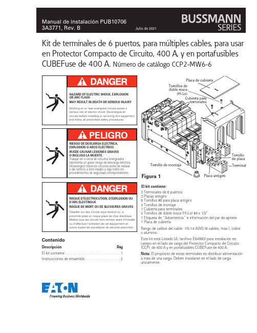
El kit contiene:Kit de terminales de 6 puertos, para múltiples cables, para usar en Protector Compacto de Circuito, 400 A, y en portafusibles CUBEFuse de 400 A. Número de catálogo CCP2-MW6-6Cubierta para terminalesTornillos de doble rosca(Hi-Lo)TerminalTornillo de montajeTornillo de placaPlaca antigiroFigura 1ContenidoDescripciónPág...........................1Instrucciones de ensamble (2)El kit contiene: 3 Terminales de 6 puertos 3 Placas antigiro6 Tornillos #6 para placa antigiro 3 Tornillos de montaje 1 Cubierta para terminales2 Tornillos de doble rosca (Hi-Lo) #4 x 1/2"1 Etiqueta de “Advertencia” e información del par de apriete 1 Placa de cubiertaRango de calibre del cable: 1/0-14 AWG (6 cables, máx.), cobre o aluminioEste kit está Listado UL (archivo E64983) para instalación en campo en el lado de carga del Protector Compacto de Circuito (CCP), de 400 A y en portafusibles CUBEFuse de 400 A.Nota: El propósito de estas terminales es distribuir alimentación a más de una carga. Deben instalarse en el lado de carga únicamente.CCP2-MW6-6Manual de instalación PUB107063A3771, Rev. BJulio de 202110 a 14 (6 a 2.5) 3.9 (35)8 (10)4.5 (40)4 a 6 (25 a 16)5.0 (45)1/0 a 2 (50 a 35)5.6 (50)Medio 1-3/8 a 1-1/2Inferior 2 a 2-1/8ADVERTENCIA:LOS CONDUCTORES DIMENSIONADOS PARA CORRIENTES DE CARGA INFERIORES A LA CLASIFICACIÓN DEL FUSIBLE NO ESTARÁN PROTEGIDOS POR EL FUSIBLE.CADA CABLE DE CARGA DEBE ESTAR PROTEGIDO POR UN DISPOSITIVO DE PROTECCIÓN CONTRA SOBRECORRIENTE, INDIVIDUAL, Y CUMPLIR CON LOS REQUISITOS ADICIONALES CORRESPONDIENTES DEL NEC.Instrucciones de ensambleSi el CCP o el portafusible CUBEFuse ya está instalado en el equipo, debe desmontarlo del equipo para instalar este kit. El kit está diseñado para usarse únicamente en el lado de carga. Vea la Figura 1.1. Quite y deseche las terminales para cable existentes en el lado de carga del CCP o del portafusible CUBEFuse, si es necesario.2. Coloque la placa antigiro en la terminal y asegúrela con los tornillos#6. Aplique un par de apriete de 0.6 N•m (5 lb-pulg).NOTA. Utilice únicamente los tornillos de montaje que vienen con el kit. No los sustituya, pues podría no cumplir con la separación eléctrica.3. Ensamble la terminal en la parte superior, como se muestra, y apriétela rmemente con el tornillo de montaje. Aplique un par de apriete de 22.0 N•m (200 lb-pulg).4. Use la placa de la cubierta (con sello de alambre únicamente).En este momento, el CCP o el portafusible CUBEFuse puedeinstalarse en el equipo. Después de instalarlo, coloque la cubierta de terminales con los tornillos de doble rosca (Hi-Lo). Vea la Figura 1.CABLEADO EN CAMPONota. Podría no ser posible instalar cables de mayor calibre en los puertos de terminales adyacentes debido al grosor del aislamiento del cable. Utilice únicamente conexiones quepermitan insertar los cables sin interferencia de aislamiento entre cables en la terminal. Cuando se inserta completamente en la terminal, el aislamiento del cable debe estar a menos de 1/8". Retire el aislamiento de los cables las longitudes que se indican a continuación.i K tC a n t i d a d 1C C P S E R I E B U S S M A N NC C P 2-M W 6-6P a r a i n t e r r u p t o r d e 400 A y p o r t a f u s i b l e C U B E F u s e d e 400 AT E R M I N A L E S P A R A M ÚL T I P L E S C A B L E SP A R A C C P D E 400 A Y P O R T A F U S I B L E C U B E F U S E D E 400 A ,S E R I E B U S S M A N NH e c h o e n E s t a d o s U n i d o sEaton y Bussmann son marcas comerciales de Eaton, registradas en Estado Unidos y otros países. No se permite el uso de las marcas comerciales de Eaton sin el previo consentimiento por escrito de Eaton.Estas instrucciones se publican únicamente con propósitos informativos y no deben considerarse como exhaustivas.Para mayor información, consulte a Ingeniería de Aplicaciones en el teléfono 800-8-387369, lunes a viernes, de 8:00 a.m. a 6:00 p.m., Hora del Centro, o envíe un correo electrónico a ********************La venta del producto que se presenta en este documento estásujeta a los términos y condiciones descritos en las políticas de venta correspondientes de la División Bussmann y otros acuerdoscontractuales entre las partes. Este documento no pretende ampliar ni agrega algún contrato de este tipo. El contrato entre el comprador y la División Bussmann es el único documento que rige los derechos del comprador de este equipo.LA INFORMACIÓN, LAS RECOMENDACIONES Y LASDESCRIPCIONES CONTENIDAS EN EL PRESENTE DOCUMENTO NO CONSTITUYEN GARANTÍA ALGUNA, EXPRESA O IMPLÍCITA, INCLUIDAS LAS GARANTÍAS DE IDONEIDAD PARA UNPROPÓSITO DETERMINADO O DE COMERCIABILIDAD, Y LAS GARANTÍAS QUE SURJAN DURANTE EL TRANSCURSO DE LA NEGOCIACIÓN O DE LOS USOS COMERCIALES.En ningún caso la División Bussmann será responsable ante elcomprador o usuario por contrato, por agravio (incluida la negligencia), por responsabilidad estricta o de otra manera por cualquier daño o pérdida especial, indirecta, incidental o consecuente, incluido pero no limitado a daño o pérdida de uso de equipo, instalaciones, planta o sistema de energía, costo de capital, pérdida de energía, gastos adicionales en el uso de instalaciones de energía existenteso reclamaciones contra el comprador o usuario por parte de susclientes como resultado del uso de la información, recomendaciones y descripción aquí contenidas.0517********Eaton1000 Eaton Boulevard Cleveland. OH 44122United States División Bussmann Poniente 148 núm. 933Industrial VallejoCiudad de México, 02300Eaton.mx/bussmannseries© 2021 EatonTodos los derechos son reservados.Impreso en México.Publicación Núm. PUB10706-spanish 3A3771Julio de 2021。
电源监控器手册说明书

Supply:Supply:Supply:Mounting Output Frequency 208 to 240 VAC 380 to 415 VAC 380 to 480 VAC DIN-rail 2 x SPDT 50 - 60 Hz DPC 71 D M23DPC 71 D M48Plug-in2x SPDT50 - 60 HzPPC 71 D M23PPC 71 D M48Product Description•TRMS 3-phase over and under voltage,phase sequence, phase loss, asymmetry and tolerance monitoring relay•Detect when all 3 phases are present and have the correct sequence•Detect if all the 3-phase-phase or phase-neutral voltages are within the set limits•Detect if asymmetry and tolerance are within the set value•Separately adjustable setpoints•Separately adjustable delay functions (0.1 to 30 s)•Output: 2 x 5 A relay SPDT NE•For mounting on DIN-rail in accordance withDIN/EN 50 022 (DPC71) or plug-in module (PPC71)•35.5 mm Euronorm housing (DPC71) or 35.5 mm plug-in module (PPC71)•LED indication for relays, alarm and power supply ONType Selection3-phase or 3-phase+neutral line voltage monitoring relay for phase sequence, phase loss, asymmetry, tolerance,over and under voltage (sep-arately adjustable set points)with built-in time delay func-tion.Supply ranges from 208 to 480 VAC covered by two multivoltage relays.DPC71PPC71Input SpecificationsOutput SpecificationsMonitoring RelaysTrue RMS 3-Phase, 3-Phase+N, Multifunction Types DPC71, PPC71DPC71, PPC71Supply SpecificationsGeneral SpecificationsMode of OperationAsymmetry definition.Asymmetry is an indicator of the mains quality and it is defined as the absolute val-ue of the max imum devia-tion among the mains volt-ages, divided by the nominal voltage of the 3-phase sys-tem. The definition changes according to the voltage ref-erence:1)in case of measuring phase-phase voltages:max |∆V PH-PH |V ∆NOM2)in case of measuring phase-neutral voltages:max |∆V PH-N |VNOMTolerance definition.T olerance is another indicator of the mains quality and it is definied as the absolute val-ue of the maximum deviation of the mains voltages from the nominal voltage, divided by the nominal voltage of the 3-phase system. The defini-tion changes according to the voltage reference:1)in case of measuring phase-phase voltages:max |V ∆NOM -V PH-PH |V ∆NOM2)in case of measuring phase-neutral voltages:max |VNOM -V PH-N |VNOMx 100x 100x 100x 100General Specifications (cont.)DPC71, PPC71Mode of Operation (cont.)Connected to the 3 phases (and neutral) DPC71 and PPC71 operate when all 3 phases are present at the same time and the phase sequence is correct. It can be decided whether to mon-itor upper and lower voltage level of each phase or their asymmetry and tolerance. Voltage level monitoring:if one or more phase-phase or phase-neutral voltage ex ceed the upper set level or drop below the lower set level, the red LED starts flashing 2 Hz and the respective output relay releases after the set time period.Asymmetry and tolerancemonitoring:if one or more phase-phaseor phase-neutral voltageexceed the set levels the redLED starts flashing 2 Hz andthe respective output relayreleases after the set timeperiod.Note:For both functions, ifthe phase sequence iswrong or one phase is lost,both output relays releaseimmediately. Only 200 msdelay occurs. The failure isindicated by the red LEDflashing 5 Hz during thealarm condition.Example 1(Mains monitoring - over andunder phase-phase voltage)The relay monitors over andunder voltage, phase lossand correct phasesequence.Example 2(Motor monitoring - startingand operating load - asym-metry and tolerance ofphase-neutral voltage)DPC71 and PPC71 ensurecorrect starting and operat-ing conditions. They monitorthe voltage level, phasesequence (correct directionof the motor rotation) andasymmetry.Frequent failures are fuseblowing and incorrect volt-age level. In case of fuseblowing the motor regener-ates a voltage in the inter-rupted phase. The relaydetects the failure andreacts due to e x cessiveimbalance among the phas-es.Function/Range/Level/Time SettingAdjust the input range set-ting the DIP-switches 3 and 4. Select the desired func-tion setting the DIP-switches 5and 6 as shown below. To access the DIP-switches open the plastic cover using a screwdriver as shown below.Upper knobs: Setting of upper ()and lower () level or setting of asymmetry (ASY) and toler-ance ( ) on relative scale. Lower knobs:Setting of delay on alarm times (DELAY 1, DELAY 2) on absolute scale:0.1 to 30s.DPC71, PPC71Operation DiagramsOver and undervoltage monitoring (2 x SPDT relays)Asymmetry and tolerance monitoring (2 x SPDT relays)DPC71, PPC71Operation Diagrams (cont.)Wiring DiagramsDPC71, PPC71 Dimensions。