MAX5433LETA中文资料
MAX3232中文资料.pdf
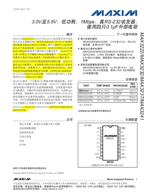
MAX3222/MAX3232/MAX3237/MAX32413.0V至5.5V、低功耗、1Mbps、真RS-232收发器,使用四只0.1µF外部电容________________________________________________________________Maxim Integrated Products119-0273; Rev 7; 1/07MegaBaud和UCSP是Maxim Integrated Products, Inc.的商标。
本文是英文数据资料的译文,文中可能存在翻译上的不准确或错误。
如需进一步确认,请在您的设计中参考英文资料。
有关价格、供货及订购信息,请联络Maxim亚洲销售中心:10800 852 1249 (北中国区),10800 152 1249 (南中国区),或访问Maxim的中文网站:。
M A X 3222/M A X 3232/M A X 3237/M A X 32413.0V至5.5V、低功耗、1Mbps、真RS-232收发器,使用四只0.1µF外部电容2_______________________________________________________________________________________ABSOLUTE MAXIMUM RATINGSELECTRICAL CHARACTERISTICS(V CC = +3.0V to +5.5V, C1–C4 = 0.1µF (Note 2), T A = T MIN to T MAX , unless otherwise noted. Typical values are at T A = +25°C.)Stresses beyond those listed under “Absolute Maximum Ratings” may cause permanent damage to the device. These are stress ratings only, and functional operation of the device at these or any other conditions beyond those indicated in the operational sections of the specifications is not implied. Exposure to absolute maximum rating conditions for extended periods may affect device reliability.Note 1:V+ and V- can have a maximum magnitude of 7V, but their absolute difference cannot exceed 13V.V CC ...........................................................................-0.3V to +6V V+ (Note 1)...............................................................-0.3V to +7V V- (Note 1)................................................................+0.3V to -7V V+ + V- (Note 1)...................................................................+13V Input VoltagesT_IN, SHDN , EN ...................................................-0.3V to +6V MBAUD...................................................-0.3V to (V CC + 0.3V)R_IN.................................................................................±25V Output VoltagesT_OUT...........................................................................±13.2V R_OUT....................................................-0.3V to (V CC + 0.3V)Short-Circuit DurationT_OUT....................................................................ContinuousContinuous Power Dissipation (T A = +70°C)16-Pin TSSOP (derate 6.7mW/°C above +70°C).............533mW 16-Pin Narrow SO (derate 8.70mW/°C above +70°C)....696mW 16-Pin Wide SO (derate 9.52mW/°C above +70°C)........762mW 16-Pin Plastic DIP (derate 10.53mW/°C above +70°C)...842mW 18-Pin SO (derate 9.52mW/°C above +70°C)..............762mW 18-Pin Plastic DIP (derate 11.11mW/°C above +70°C)..889mW 20-Pin SSOP (derate 7.00mW/°C above +70°C).........559mW 20-Pin TSSOP (derate 8.0mW/°C above +70°C).............640mW 28-Pin TSSOP (derate 8.7mW/°C above +70°C).............696mW 28-Pin SSOP (derate 9.52mW/°C above +70°C).........762mW 28-Pin SO (derate 12.50mW/°C above +70°C).....................1W Operating Temperature RangesMAX32_ _C_ _.....................................................0°C to +70°C MAX32_ _E_ _ .................................................-40°C to +85°C Storage Temperature Range.............................-65°C to +150°C Lead Temperature (soldering, 10s).................................+300°CMAX3222/MAX3232/MAX3237/MAX32413.0V至5.5V、低功耗、1Mbps、真RS-232收发器,使用四只0.1µF外部电容_______________________________________________________________________________________3TIMING CHARACTERISTICS—MAX3222/MAX3232/MAX3241(V CC = +3.0V to +5.5V, C1–C4 = 0.1µF (Note 2), T A = T MIN to T MAX , unless otherwise noted. Typical values are at T A = +25°C.)ELECTRICAL CHARACTERISTICS (continued)(V CC = +3.0V to +5.5V, C1–C4 = 0.1µF (Note 2), T A = T MIN to T MAX , unless otherwise noted. Typical values are at T A = +25°C.)A X 3222/M A X 3232/M A X 3237/M A X 32413.0V至5.5V、低功耗、1Mbps、真RS-232收发器,使用四只0.1µF外部电容4_______________________________________________________________________________________典型工作特性Ω, T A = +25°C, unless otherwise noted.)LOAD CAPACITANCE (pF)0246810121416182022150MAX3222/MAX3232SLEW RATEvs. LOAD CAPACITANCELOAD CAPACITANCE (pF)S L E W R A T E (V /µs )20003000100040005000510152025303540MAX3222/MAX3232SUPPLY CURRENT vs. LOAD CAPACITANCEWHEN TRANSMITTING DATALOAD CAPACITANCE (pF)S U P P L Y C U R R E N T (m A )20003000100040005000TIMING CHARACTERISTICS—MAX3237(V CC = +3.0V to +5.5V, C1–C4 = 0.1µF (Note 2), T A = T MIN to T MAX , unless otherwise noted. Typical values are at T A = +25°C.)Note 2:MAX3222/MAX3232/MAX3241: C1–C4 = 0.1µF tested at 3.3V ±10%; C1 = 0.047µF, C2–C4 = 0.33µF tested at 5.0V ±10%.MAX3237: C1–C4 = 0.1µF tested at 3.3V ±5%; C1–C4 = 0.22µF tested at 3.3V ±10%; C1 = 0.047µF, C2–C4 = 0.33µF tested at 5.0V ±10%.Note 3:Transmitter input hysteresis is typically 250mV.MAX3222/MAX3232/MAX3237/MAX32413.0V至5.5V、低功耗、1Mbps、真RS-232收发器,使用四只0.1µF外部电容_______________________________________________________________________________________5-7.5-5.0-2.502.55.07.50MAX3241TRANSMITTER OUTPUT VOLTAGEvs. LOAD CAPACITANCELOAD CAPACITANCE (pF)T R A N S M I T T E R O U T P U T V O L T A G E (V )2000300010004000500046810121416182022240MAX3241SLEW RATEvs. LOAD CAPACITANCELOAD CAPACITANCE (pF)S L E W R A T E (V /µs )20003000100040005000510152025303545400MAX3241SUPPLY CURRENT vs. LOADCAPACITANCE WHEN TRANSMITTING DATALOAD CAPACITANCE (pF)S U P P L Y C U R R E N T (m A )20003000100040005000-7.5-5.0-2.502.55.07.50MAX3237TRANSMITTER OUTPUT VOLTAGE vs. LOAD CAPACITANCE (MBAUD = GND)LOAD CAPACITANCE (pF)T R A N S M I T T E R O U T P U T V O L T A G E (V )200030001000400050000102030504060700MAX3237SLEW RATE vs. LOAD CAPACITANCE(MBAUD = V CC )LOAD CAPACITANCE (pF)S L E W R A T E (V /µs )500100015002000-7.5-5.0-2.502.55.07.50MAX3237TRANSMITTER OUTPUT VOLTAGE vs. LOAD CAPACITANCE (MBAUD = V CC )LOAD CAPACITANCE (pF)T R A N S M I T T E R O U T P U T V O L T A G E (V )5001000150020001020304050600MAX3237SUPPLY CURRENT vs.LOAD CAPACITANCE (MBAUD = GND)LOAD CAPACITANCE (pF)S U P P L Y C U R R E N T (m A )200030001000400050000246810120MAX3237SLEW RATE vs. LOAD CAPACITANCE(MBAUD = GND)LOAD CAPACITANCE (pF)S L E W R A T E (V /µs )2000300010004000500010302040506070MAX3237SKEW vs. LOAD CAPACITANCE(t PLH - t PHL )LOAD CAPACITANCE (pF)1000150050020002500____________________________________________________________________典型工作特性(续)(V CC = +3.3V, 235kbps data rate, 0.1µF capacitors, all transmitters loaded with 3k Ω, T A = +25°C, unless otherwise noted.)M A X 3222/M A X 3232/M A X 3237/M A X 32413.0V至5.5V、低功耗、1Mbps、真RS-232收发器,使用四只0.1µF外部电容6_________________________________________________________________________________________________________________________________________________________________引脚说明MAX3222/MAX3232/MAX3237/MAX32413.0V至5.5V、低功耗、1Mbps、真RS-232收发器,使用四只0.1µF外部电容_______________________________________________________________________________________7_______________________________详细说明双电荷泵电压转换器MAX3222/MAX3232/MAX3237/MAX3241的内部电源由两路稳压型电荷泵组成,只要输入电压(V CC )在3.0V至5.5V范围以内,即可提供+5.5V (倍压电荷泵)和-5.5V (反相电荷泵)输出电压。
MAX6953EAX+;MAX6953EAX+T;中文规格书,Datasheet资料

General DescriptionThe MAX6953 is a compact cathode-row display driver that interfaces microprocessors to 5 ✕7 dot-matrix LED displays through an I 2C™-compatible serial interface.The MAX6953 drives up to four digits (140 LEDs).Included on-chip are an ASCII 104-character font, mul-tiplex scan circuitry, column and row drivers, and static RAM that stores each digit, as well as font data for 24user-definable characters. The segment current for the LEDs is set by an internal digit-by-digit digital bright-ness control.The device includes a low-power shutdown mode, seg-ment blinking (synchronized across multiple drivers, if desired), and a test mode that forces all LEDs on. The LED drivers are slew-rate limited to reduce EMI.For an SPI™-compatible version, refer to the MAX6952data sheet. An EV kit is available for the MAX6952.ApplicationsMessage Boards Medical Equipment Industrial Displays Audio/Video Equipment Gaming MachinesFeatures♦400kbps 2-Wire Interface Compatible with I 2C♦ 2.7V to 5.5V Operation♦Drives 4 Monocolor or 2 Bicolor Cathode-Row 5 ✕7 Matrix Displays ♦Built-In ASCII 104-Character Font ♦24 User-Definable Characters Available ♦Automatic Blinking Control for Each Segment ♦70µA Low-Power Shutdown (Data Retained)♦16-Step Digital Brightness Control ♦Display Blanked on Power-Up♦Slew-Rate-Limited Segment Drivers for Lower EMI ♦36-Pin SSOP and 40-Pin DIP Packages ♦Extended Temperature Range as StandardMAX69532-Wire Interfaced, 2.7V to 5.5V , 4-Digit 5 ✕7Matrix LED Display Driver________________________________________________________________Maxim Integrated Products1Ordering InformationTypical Application Circuit19-2312; Rev 3; 3/04For pricing, delivery, and ordering information,please contact Maxim/Dallas Direct!at 1-888-629-4642, or visit Maxim’s website at .I 2C is a trademark of Philips Corp.SPI is a trademark of Motorola, Inc.Pin Configurations appear at end of data sheet.M A X 69532-Wire Interfaced, 2.7V to 5.5V , 4-Digit 5 ✕7Matrix LED Display Driver 2_______________________________________________________________________________________ABSOLUTE MAXIMUM RATINGSDC ELECTRICAL CHARACTERISTICSStresses beyond those listed under “Absolute Maximum Ratings” may cause permanent damage to the device. These are stress ratings only, and functional operation of the device at these or any other conditions beyond those indicated in the operational sections of the specifications is not implied. Exposure to absolute maximum rating conditions for extended periods may affect device reliability.Voltage (with Respect to GND)V+.............................................................................-0.3V to +6V All Other Pins................................................-0.3V to (V+ + 0.3V)O0–O13 Sink Current.......................................................500mA O14–O23 Source Current..................................................50mA Continuous Power Dissipation (T A = +70°C)36-Pin SSOP (derate 11.8mW/°C above +70°C).....941.2mW 40-Pin PDIP (derate 16.7mW/°C above +70°C)........1333mWOperating Temperature RangeMAX6953E......................................................-40°C to +85°C Junction Temperature......................................................+150°C Storage Temperature Range.............................-65°C to +150°C Lead Temperature (soldering, 10s).................................+300°CMAX69532-Wire Interfaced, 2.7V to 5.5V , 4-Digit 5 ✕7Matrix LED Display Driver_______________________________________________________________________________________3DC ELECTRICAL CHARACTERISTICS (continued)MAX6953 TIMING CHARACTERISTICSTypical Operating Characteristics(Typical application circuit, V+ = 3.3V, LED forward voltage = 2.4V, scan limit set to 4 digits, T A = +25°C, unless otherwise noted.)M A X 69532-Wire Interfaced, 2.7V to 5.5V , 4-Digit 5 ✕7Matrix LED Display Driver 4_______________________________________________________________________________________MAX6953 TIMING CHARACTERISTICS (continued)(V+ = 2.7V to 5.5V, T A = T MIN to T MAX , unless otherwise noted.) (Note 1)Note 1:All parameters tested at T A = +25°C. Specifications over temperature are guaranteed by design. Note 2:Guaranteed by design.Note 3:A master device must provide a hold time of at least 300ns for the SDA signal (referred to V IL of the SCL signal) in order tobridge the undefined region of SCL’s falling edge.Note 4:C B = total capacitance of one bus line in pF. t R and t F measured between 0.3V+ and 0.7V+.Note 5:I SINK ≤6mA. C B = total capacitance of one bus line in pF. t R and t F measured between 0.3V+ and 0.7V+.Note 6:Input filters on the SDA and SCL inputs suppress noise spikes less than 50ns.3.803.904.104.004.204.30-40-2020406080INTERNAL OSCILLATOR FREQUENCY vs. TEMPERATURETEMPERATURE (°C)O S C I L L A T O R F R E Q U E N C Y (M H z )INTERNAL OSCILLATOR FREQUENCYvs. SUPPLY VOLTAGEM A X 6953 t o c 02SUPPLY VOLTAGE (V)O S C I L L A T O R F R E Q U E N C Y (M H z )4.53.53.73.83.94.04.14.24.34.43.62.55.500.51.51.02.02.5400200600800INTERNAL OSCILLATORWAVEFORM AT OSC (PIN 19 OR 21)TIMELINE (ns)V O L T A G E A T O S C (V )MAX69532-Wire Interfaced, 2.7V to 5.5V , 4-Digit 5 ✕7Matrix LED Display Driver808595901001052.53.53.04.04.55.05.5DEAD CLOCK OSCILLATOR FREQUENCYvs. SUPPLY VOLTAGEM A X 6953 t o c 04SUPPLY VOLTAGE (V)O S C I L L A T O R F R E Q U E N C Y (k H z )0.950.970.960.990.981.001.012.5 3.5 4.03.0 4.5 5.0 5.5OUTPUT SOURCE CURRENT vs. SUPPLY VOLTAGEM A X 6953 t o c 05SUPPLY VOLTAGE (V)C U R R E N T N O R M A L I Z ED T O 40m A WAVEFORMS AT O2 (PIN 3) AND O14(PIN 28) V+ = 3.3V, 8/16 INTENSITYGROUND FORANODE (PIN 014)M A X 6953 t o c 06GROUND FOR CATHODE (PIN 03)200µs/divTypical Operating Characteristics (continued)(Typical application circuit, V+ = 3.3V, LED forward voltage = 2.4V, scan limit set to 4 digits, T A = +25°C, unless otherwise noted.)M A X 69532-Wire Interfaced, 2.7V to 5.5V , 4-Digit 5 ✕7Matrix LED Display DriverDetailed DescriptionThe MAX6953 is a serially interfaced display driver that can drive four digits of 5 ✕7 cathode-row dot-matrix dis-plays. The MAX6953 can drive either four monocolor digits (Table 1) or two bicolor digits (Table 2). The MAX6953 includes a 128-character font map compris-ing 104 predefined characters and 24 user-definable characters. The predefined characters follow the Arial font, with the addition of the following common symbols:£, <, ¥, °, µ, ±, ↑, and ↓. The 24 user-definable charac-ters are uploaded by the user into on-chip RAM through the serial interface and are lost when the device is pow-ered down. Figure 1 is the MAX6953 functional diagram.Serial InterfaceSerial AddressingThe MAX6953 operates as a slave that sends and receives data through an I 2C-compatible 2-wire inter-face. The interface uses a serial data line (SDA) and a serial clock line (SCL) to achieve bidirectional commu-nication between master(s) and slave(s). A master (typ-ically a microcontroller) initiates all data transfers to and from the MAX6953, and generates the SCL clock that synchronizes the data transfer (Figure 2).The MAX6953 SDA line operates as both an input and an open-drain output. A pullup resistor, typically 4.7k Ω,is required on the SDA. The MAX6953 SCL line oper-ates only as an input. A pullup resistor, typically 4.7k Ω,is required on SCL if there are multiple masters on the 2-wire interface, or if the master in a single-master sys-tem has an open-drain SCL output.Each transmission consists of a START condition (Figure 3) sent by a master, followed by the MAX69537-bit slave address plus R/W bit (Figure 6), a register address byte, 1 or more data bytes, and finally a STOP condition (Figure 3).Start and Stop ConditionsBoth SCL and SDA remain high when the interface is not busy. A master signals the beginning of a transmis-sion with a START (S) condition by transitioning SDA from high to low while SCL is high. When the master has finished communicating with the slave, it issues a STOP (P) condition by transitioning the SDA from low to high while SCL is high. The bus is then free for another transmission (Figure 3).MAX69532-Wire Interfaced, 2.7V to 5.5V , 4-Digit 5 ✕7Matrix LED Display Driver_______________________________________________________________________________________7Bit TransferOne data bit is transferred during each clock pulse.The data on the SDA line must remain stable while SCL is high (Figure 4).AcknowledgeThe acknowledge bit is a clocked 9th bit that the recipi-ent uses to handshake receipt of each byte of data (Figure 5). Thus, each byte transferred effectively requires 9 bits. The master generates the 9th clock pulse, and the recipient pulls down SDA during the acknowledge clock pulse, such that the SDA line is sta-ble low during the high period of the clock pulse. When the master is transmitting to the MAX6953, the MAX6953 generates the acknowledge bit because the MAX6953 is the recipient. When the MAX6953 is trans-mitting to the master, the master generates the acknowledge bit because the master is the recipient.Slave AddressThe MAX6953 has a 7-bit-long slave address (Figure 6). The eighth bit following the 7-bit slave address is the R/W bit. It is low for a write command, high for a read command.The first 3 bits (MSBs) of the MAX6953 slave address are always 101. Slave address bits A3, A2, A1, and A0are selected by the address input pins AD1 and AD0.These two input pins may be connected to GND, V+,SDA, or SCL. The MAX6953 has 16 possible slave addresses (Table 3) and therefore a maximum of 16MAX6953 devices may share the same interface.Message Format for WritingA write to the MAX6953 comprises the transmission of the MAX6953's slave address with the R/W bit set to zero, followed by at least 1 byte of information. The first byte of information is the command byte, which deter-mines which register of the MAX6953 is to be written by the next byte, if received. If a STOP condition is detect-ed after the command byte is received, then the MAX6953 takes no further action (Figure 7) beyond storing the command byte.Any bytes received after the command byte are data bytes. The first data byte goes into the internal register of the MAX6953 selected by the command byte (Figure 8). If multiple data bytes are transmitted before a STOP condition is detected, these bytes are generally stored in subsequent MAX6953 internal registers because the command byte address generally autoincrements (Table 4) (Figure 9).Message Format for ReadingThe MAX6953 is read using the MAX6953's internally stored command byte as address pointer, the same way the stored command byte is used as address pointer for a write. The pointer generally autoincre-ments after each data byte is read using the same rules as for a write (Table 4). Thus, a read is initiated by first configuring the MAX6953's command byte by perform-ing a write (Figure 7). The master can now read n con-secutive bytes from the MAX6953, with the first data byte being read from the register addressed by the ini-tialized command byte (Figure 9).When performingFigure 2. 2-Wire Serial Interface Timing DetailsM A X 69532-Wire Interfaced, 2.7V to 5.5V , 4-Digit 5 ✕7Matrix LED Display Driver 8_______________________________________________________________________________________Figure 6. Slave AddressFigure 3. Start and Stop ConditionsFigure 4. Bit TransferFigure 5. AcknowledgeMAX69532-Wire Interfaced, 2.7V to 5.5V , 4-Digit 5 ✕7Matrix LED Display Driver_______________________________________________________________________________________9read-after-write verification, reset the command byte's address because the stored byte address generally is autoincremented after the write (Table 4).Operation with Multiple MastersIf the MAX6953 is operated on a 2-wire interface with multiple masters, a master reading the MAX6953should use a repeated start between the write, which sets the MAX6953's address pointer, and the read(s)that takes the data from the location(s). This is because it is possible for master 2 to take over the bus after master 1 has set up the MAX6953's address pointer but before master 1 has read the data. If master 2 subse-quently changes the MAX6953's address pointer, then master 1's delayed read may be from an unexpected location.Command Address AutoincrementingAddress autoincrementing allows the MAX6953 to be configured with the shortest number of transmissions by minimizing the number of times the command byte needs to be sent. The command address or the font pointer address stored in the MAX6953 generally incre-ments after each data byte is written or read (Table 4).Digit RegistersThe MAX6953 uses eight digit registers to store the char-acters that the user wishes to display on the four 5 ✕7LED digits. These digit registers are implemented with two planes of 4 bytes, called P0 and P1. Each LED digit is represented by 2 bytes of memory, 1 byte in plane P0and the other in plane P1. The digit registers are mapped so that a digit’s data can be updated in plane P0, or plane P1, or both planes at the same time (Table 5).If the blink function is disabled through the Blink Enable Bit E (Table 10) in the configuration register, then the digit register data in plane P0 is used to multiplex the display. The digit register data in P1 is not used. If the blink function is enabled, then the digit register data in both plane P0 and plane P1 are alternately used to mul-tiplex the display. Blinking is achieved by multiplexing the LED display using data planes P0 and P1 on alter-nate phases of the blink clock (Table 11).The data in the digit registers does not control the digit segments directly. Instead, the register data is used to address a character generator, which stores the data of a 128-character font (Table 15). The lower 7 bits of the digit data (D6 to D0) select the character from the font.The most-significant bit of the register data (D7) selects whether the font data is used directly (D7 = 0) or whether the font data is inverted (D7 = 1). The inversion feature can be used to enhance the appearance of bicolor displays by displaying, for example, a red char-acter on a green background.Display Blink ModeThe display blinking facility, when enabled, makes the driver flip automatically between displaying the digit register data in planes P0 and P1. If the digit register data for any digit is different in the two planes, then thatFigure 7. Command Byte ReceivedFigure 8. Command and Single Data Byte ReceivedM A X 69532-Wire Interfaced, 2.7V to 5.5V , 4-Digit 5 ✕7Matrix LED Display Driver 10______________________________________________________________________________________Figure 9. n Data Bytes Receiveddigit appears to flip between two characters. To make a character appear to blink on or off, write the character to one plane, and use the blank character (0x20) for the other plane. Once blinking has been configured, it con-tinues automatically without further intervention.Blink SpeedThe blink speed is determined by frequency of the mul-tiplex clock, OSC, and by setting the Blink Rate Selection Bit B (Table 9) in the configuration register.The Blink Rate Selection Bit B sets either fast or slow blink speed for the whole display.Initial Power-UpOn initial power-up, all control registers are reset, the display is blanked, intensities are set to minimum, and shutdown is enabled (Table 6).Configuration RegisterThe configuration register is used to enter and exit shut-down, select the blink rate, globally enable and disable the blink function, globally clear the digit data, and reset the blink timing (Table 7).Shutdown Mode (S Data Bit D0) FormatThe S bit in the configuration register selects shutdown or normal operation. The display driver can be pro-grammed while in shutdown mode, and shutdown mode is overridden when in the display test mode. For normal operation, the S bit should be set to 1 (Table 8).Blink Rate Selection (B Data Bit D2) FormatThe B bit in the configuration register selects the blink rate. This is the speed that the segments alternate between plane P0 and plane P1 refresh data. The blink rate is determined by the frequency of the multiplex clock OSC, in addition to the setting of the B bit (Table 9).分销商库存信息:MAXIMMAX6953EAX+MAX6953EAX+T。
MAX4313EUA+T中文资料
元器件交易网
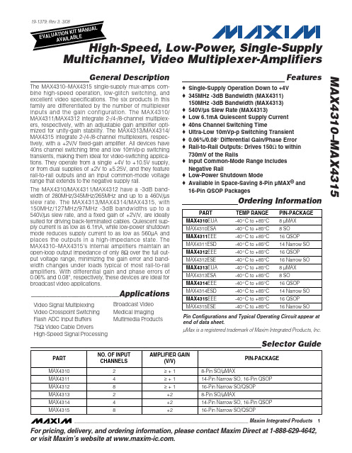
MAX4310–MAX4315
High-Speed, Low-Power, Single-Supply Multichannel, Video Multiplexer-Amplifiers
ABSOLUTE MAXIMUM RATINGS
Supply Voltage (VCC to VEE) .................................................12V Input Voltage....................................(VEE - 0.3V) to (VCC + 0.3V) All Other Pins ...................................(VEE - 0.3V) to (VCC + 0.3V) Output Current................................................................±120mA Short-Circuit Duration (VOUT to GND, VCC or VEE)....Continuous Continuous Power Dissipation (TA = +70°C)
________________________________________________________________ Maxim Integrated Products 1
For pricing, delivery, and ordering information, please contact Maxim Direct at 1-888-629-4642, or visit Maxim’s website at .
MAX1483ESA+中文资料

元器件交易网
µMAX is a registered trademark of Maxim Integrated products, Inc.
________________________________________________________________ Maxim Integrated Products 1
元器件交易网
19-0367; Rev 1; 5/06
MAX1482/MAX1483
20µA, 1⁄8-Unit-Load, Slew-Rate-Limited RS-485 Transceivers
_______________General Description
The MAX1482 and MAX1483 are low-power transceivers for RS-485 and RS-422 communication. Both feature slew-rate-limited drivers that minimize EMI and reduce reflections caused by improperly terminated cables. Data rates are guaranteed up to 250kbps. The MAX1482/MAX1483 draw only 20µA of supply current. Additionally, they have a low-current shutdown mode that consumes only 0.1µA. Both parts operate from a single +5V supply. Drivers are short-circuit current limited and are protected against excessive power dissipation by thermal shutdown circuitry that places the driver outputs into a high-impedance state. The receiver input has a fail-safe feature that guarantees a logic-high output if the input is open circuit. The MAX1482 is full duplex and the MAX1483 is half duplex. Both parts have a 1⁄8-unit-load input impedance that guarantees up to 256 transceivers on the bus.
数字电位器-IIC-MAX5432
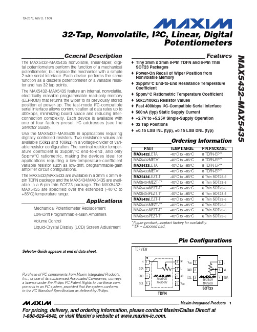
32-Tap, Nonvolatile, I2C, Linear, Digital Potentiometers MAX5432–MAX5435
ABSOLUTE MAXIMUM RATINGS
VDD to GND ...........................................................-0.3V to +6.0V SDA, SCL to GND..................................................-0.3V to +6.0V A0, H, L, and W to GND .............................-0.3V to (VDD + 0.3V) Maximum Continuous Current into H, L, and W MAX5432/MAX5434.....................................................±1.3mA MAX5433/MAX5435.....................................................±0.6mA Input/Output Latchup Immunity........................................±50mA Continuous Power Dissipation (TA = +70°C) 6-Pin Thin SOT23 (derate 9.1mW/°C above +70°C) ....727mW 8-Pin TDFN (derate 24.4mW/°C above +70°C) .........1951mW Operating Temperature Range ...........................-40°C to +85°C Junction Temperature ......................................................+150°C Storage Temperature Range .............................-60°C to +150°C Lead Temperature (soldering, 10s) .................................+300°C
MAX13103 芯片数据手册说明书

MJD200 (NPN),MJD210 (PNP)Complementary Plastic Power TransistorsNPN/PNP Silicon DPAK For Surface Mount ApplicationsDesigned for low voltage, low−power, high−gain audio amplifier applications.Features•High DC Current Gain•Lead Formed for Surface Mount Applications in Plastic Sleeves (No Suffix)•Low Collector−Emitter Saturation V oltage•High Current−Gain − Bandwidth Product•Annular Construction for Low Leakage •EpoxyMeetsUL94V−*********•NJV Prefix for Automotive and Other Applications Requiring Unique Site and Control Change Requirements; AEC−Q101 Qualified and PPAP Capable•These Devices are Pb−Free and are RoHS CompliantMAXIMUM RATINGSRating Symbol Max UnitCollector−Base Voltage V CB40VdcCollector−Emitter Voltage V CEO25VdcEmitter−Base Voltage V EB8.0VdcCollector Current − Continuous I C 5.0AdcCollector Current − Peak I CM10AdcBase Current I B 1.0AdcTotal Power Dissipation @ T C = 25°C Derate above 25°C P D12.50.1WW/°CTotal Power Dissipation (Note 1) @ T A = 25°CDerate above 25°C P D1.40.011WW/°COperating and Storage JunctionTemperature RangeT J, T stg−65 to +150°C ESD − Human Body Model HBM3B V ESD − Machine Model MM C V Stresses exceeding Maximum Ratings may damage the device. Maximum Ratings are stress ratings only. Functional operation above the Recommended Operating Conditions is not implied. Extended exposure to stresses above the Recommended Operating Conditions may affect device reliability.1.These ratings are applicable when surface mounted on the minimum padsizes recommended.SILICONPOWER TRANSISTORS5 AMPERES25 VOLTS, 12.5 WATTSDPAKCASE 369CSTYLE 1MARKING DIAGRAMA= Assembly LocationY=YearWW=Work Weekx= 1 or 0G=Pb−Free PackageAYWWJ2x0GSee detailed ordering and shipping information in the package dimensions section on page 6 of this data sheet.ORDERING INFORMATION1BASE3EMITTERCOLLECTOR2,412341BASE3EMITTERCOLLECTOR2,4PNP NPNTHERMAL CHARACTERISTICSCharacteristic Symbol Max Unit Thermal Resistance, Junction−to−Case R q JC10°C/W Thermal Resistance, Junction−to−Ambient (Note 2)R q JA89.3°C/W 2.These ratings are applicable when surface mounted on the minimum pad sizes recommended.ELECTRICAL CHARACTERISTICS(T C = 25°C unless otherwise noted)Characteristic Symbol Min Max Unit OFF CHARACTERISTICSCollector−Emitter Sustaining Voltage (Note 3) (I C = 10 mAdc, I B = 0)V CEO(sus)25−VdcCollector Cutoff Current(V CB = 40 Vdc, I E = 0)(V CB = 40 Vdc, I E = 0, T J = 125°C)V CBO−−100100nAdcm AdcEmitter Cutoff Current (V BE = 8 Vdc, I C = 0)V EBO−100nAdcON CHARACTERISTICSC Current Gain (Note 3),(I C = 500 mAdc, V CE = 1 Vdc) (I C = 2 Adc, V CE = 1 Vdc)(I C = 5 Adc, V CE = 2 Vdc)h FE704510−180−−Collector−Emitter Saturation Voltage (Note 3) (I C = 500 mAdc, I B = 50 mAdc)(I C = 2 Adc, I B = 200 mAdc)(I C = 5 Adc, I B = 1 Adc)V CE(sat)−−−0.30.751.8VdcBase−Emitter Saturation Voltage (Note 3) (I C = 5 Adc, I B = 1 Adc)V BE(sat)− 2.5VdcBase−Emitter On Voltage (Note 3) (I C = 2 Adc, V CE = 1 Vdc)V BE(on)− 1.6VdcDYNAMIC CHARACTERISTICSCurrent−Gain − Bandwidth Product (Note 4)(I C = 100 mAdc, V CE = 10 Vdc, f test = 10 MHz)f T65−MHzOutput Capacitance(V CB = 10 Vdc, I E = 0, f = 0.1 MHz)MJD200MJD210, NJVMJD210T4G C ob−−80120pF3.Pulse Test: Pulse Width = 300 m s, Duty Cycle [ 2%.4.f T = ⎪h fe⎪• f test.Figure 1. Power DeratingT, TEMPERATURE (°C)T CPD,POWERDISSIPATION(WATTS)Figure 2. Switching Time Test Circuit2.51.51T A0.520SCOPEV CCt r, t f≤ 10 nsDUTY CYCLE = 1%D1 MUST BE FAST RECOVERY TYPE, e.g.: 1N5825 USED ABOVE I B≈ 100 mA MSD6100 USED BELOW I B≈ 100 mAR B and R C VARIED TO OBTAIN DESIRED CURRENT LEVELSFOR PNP TEST CIRCUIT,REVERSE ALL POLARITIESI C, COLLECTOR CURRENT (A)1KI C, COLLECTOR CURRENT (A)t,TIME(ns)50030020010050302010510.02Figure 3. Turn−On Time Figure 4. Turn−Off Timet,TIME(ns)32I C , COLLECTOR CURRENT (A)I C , COLLECTOR CURRENT (A)I C , COLLECTOR CURRENT (A)h F E , D C C U R R E N T G A I NFigure 5. DC Current GainFigure 6. “On” VoltageI C , COLLECTOR CURRENT (A)200400100806040IC , COLLECTOR CURRENT (A)Figure 7. Temperature Coefficients202I C , COLLECTOR CURRENT (A)1.61.20.80.4V , V O L T AG E (V O L T S )NPN MJD200PNP MJD210h F E , D C C U R R E N T G A I NV , V O L T A G E (V O L T S )21.61.20.80.4V , T E M P E R A T U R E C O E F F I C I E N T S (m V /C )°θ+ 2.5+ 2+ 1.5+ 10- 0.5- 1- 1.5- 2+ 0.5- 2.5V , T E M P E R A T U R E C O E F F I C I E N T S (m V /C )°θ+ 2.5+ 2+ 1.5+ 10- 0.5- 1- 1.5- 2+ 0.5- 2.5t, TIME (ms)r (t ), T R A N S I E N T T H E R M A L R E S I S T A N C E (N O R M A L I Z E D )Figure 8. Thermal ResponseV CE , COLLECTOR−EMITTER VOLTAGE (V)25Figure 9. Active Region Safe Operating Area13I C , C O LL E C T O R C U R R E N T (A M P )There are two limitations on the power handling ability of a transistor: average junction temperature and second breakdown. Safe operating area curves indicate I C − V CE limits of the transistor that must be observed for reliable operation; i.e., the transistor must not be subjected to greater dissipation than the curves indicate.The data of Figure 9 is based on T J(pk) = 150°C; T C is variable depending on conditions. Second breakdown pulse limits are valid for duty cycles to 10% provided T J(pk)≤ 150°C. T J(pk) may be calculated from the data in Figure 8.At high case temperatures, thermal limitations will reduce the power that can be handled to values less than the limitations imposed by second breakdown.200V R , REVERSE VOLTAGE (V)207010030Figure 10. Capacitance50C , C A P A C I T A N C E (p F )ORDERING INFORMATIONDevice Package Type Shipping†75 Units / RailMJD200G DPAK(Pb−Free)1,800 / Tape & ReelMJD200RLG DPAK(Pb−Free)2,500 / Tape & ReelMJD200T4G DPAK(Pb−Free)75 Units / RailMJD210G DPAK(Pb−Free)1,800 / Tape & ReelMJD210RLG DPAK(Pb−Free)2,500 / Tape & ReelMJD210T4G DPAK(Pb−Free)2,500 / Tape & ReelNJVMJD210T4G*DPAK(Pb−Free)†For information on tape and reel specifications, including part orientation and tape sizes, please refer to our Tape and Reel Packaging Specifications Brochure, BRD8011/D.*NJV Prefix for Automotive and Other Applications Requiring Unique Site and Control Change Requirements; AEC−Q101 Qualified and PPAP CapablePACKAGE DIMENSIONSDPAK CASE 369C ISSUE DSTYLE 1:PIN 1.BASE2.COLLECTOR3.EMITTER4.COLLECTORǒmm inchesǓSCALE 3:1*For additional information on our Pb−Free strategy and solderingdetails, please download the ON Semiconductor Soldering and Mounting Techniques Reference Manual, SOLDERRM/D.SOLDERING FOOTPRINT*DIM MIN MAX MIN MAX MILLIMETERSINCHES D 0.2350.245 5.97 6.22E 0.2500.265 6.35 6.73A 0.0860.094 2.18 2.38b 0.0250.0350.630.89c20.0180.0240.460.61b20.0300.0450.76 1.14c 0.0180.0240.460.61e 0.090 BSC 2.29 BSC b30.1800.215 4.57 5.46L4−−−0.040−−− 1.01L 0.0550.070 1.40 1.78L30.0350.0500.89 1.27Z0.155−−−3.93−−−NOTES:1.DIMENSIONING AND TOLERANCING PER ASME Y14.5M, 1994.2.CONTROLLING DIMENSION: INCHES.3.THERMAL PAD CONTOUR OPTIONAL WITHIN DI-MENSIONS b3, L3 and Z.4.DIMENSIONS D AND E DO NOT INCLUDE MOLD FLASH, PROTRUSIONS, OR BURRS. MOLDFLASH, PROTRUSIONS, OR GATE BURRS SHALL NOT EXCEED 0.006 INCHES PER SIDE.5.DIMENSIONS D AND E ARE DETERMINED AT THE OUTERMOST EXTREMES OF THE PLASTIC BODY .6.DATUMS A AND B ARE DETERMINED AT DATUM PLANE H.H 0.3700.4109.4010.41A10.0000.0050.000.13L10.108 REF 2.74 REF L20.020 BSC 0.51 BSC DETAIL AROTATED 90 CW 5ON Semiconductor and are registered trademarks of Semiconductor Components Industries, LLC (SCILLC). SCILLC owns the rights to a number of patents, trademarks,copyrights, trade secrets, and other intellectual property. A listing of SCILLC’s product/patent coverage may be accessed at /site/pdf/Patent−Marking.pdf. SCILLC reserves the right to make changes without further notice to any products herein. SCILLC makes no warranty, representation or guarantee regarding the suitability of its products for any particular purpose, nor does SCILLC assume any liability arising out of the application or use of any product or circuit, and specifically disclaims any and all liability, including without limitation special, consequential or incidental damages. “Typical” parameters which may be provided in SCILLC data sheets and/or specifications can and do vary in different applications and actual performance may vary over time. All operating parameters, including “Typicals” must be validated for each customer application by customer’s technical experts. SCILLC does not convey any license under its patent rights nor the rights of others. SCILLC products are not designed, intended, or authorized for use as components in systems intended for surgical implant into the body, or other applications intended to support or sustain life, or for any other application in which the failure of the SCILLC product could create a situation where personal injury or death may occur. Should Buyer purchase or use SCILLC products for any such unintended or unauthorized application, Buyer shall indemnify and hold SCILLC and its officers, employees, subsidiaries, affiliates, and distributors harmless against all claims, costs, damages, and expenses, and reasonable attorney fees arising out of, directly or indirectly,any claim of personal injury or death associated with such unintended or unauthorized use, even if such claim alleges that SCILLC was negligent regarding the design or manufacture of the part. SCILLC is an Equal Opportunity/Affirmative Action Employer. This literature is subject to all applicable copyright laws and is not for resale in any manner.PUBLICATION ORDERING INFORMATION。
MAX541

MAX541是美国MAXIM公司生产的D/A转换芯片,它是低功耗(1.5mW),无缓冲电压输出,能够驱动60kv的负载,用单+5V电源工作的串行16位数模转换器。
其转换时间为1μs,输出电压变换范围为0V~VREF[16]。
下图为芯片的管脚图,并将MAX541的管脚功能列于表3-3中。
表3-3 MAX541管脚功能表
引脚号引脚名称引脚功能
1 OUT DAC 电压输出
2 AGND 模拟地
3 REF 电压参考输入,链接到外接的+2.5V参
考
4 CS 芯片选择,低电平有效
5 SCLK 串行时钟输入
6 DIN 串行数据输入
7 DGND 数字地
8 VDD +5V电源电压
MAX的工作原理是:模拟输出电压VOUT的输出范围由输入不同的数字代码来有规律的控制,当输入的16位数字代码全为0时,输出电压VOUT为0。
当输入的16位数字代码全为1时,输出电压约为VREF即2.5V。
于是VOUT的变化规律是,16位数字代码从0开始,每次加1,一直到全为1,对应的输出电压一直从0开始每次增加VREF*(1/65536)。
1111 1111 1111 1111 VREF*(65535/65536)
…….
…….
1000 0000 0000 0000 VREF*(32768/65536)
…….
……
0000 0000 0000 0001 VREF*(1/65536)
0000 0000 0000 0000 VREF *( 0/65536)。
MAX333AEWP中文资料

________________________________________________________________ Maxim Integrated Products
1
For free samples & the latest literature: , or phone 1-800-998-8800. For small orders, phone 1-800-835-8769.
元器件交易网
Precision, Quad, SPDT, CMOS Analog Switch MAX333A
ABSOLUTE MAXIMUM RATINGS
V+ to V- ..................................................................................44V VIN, VCOM, VNO, VNC ......................................................V- to V+ (VNO - VNC) ............................................................................32V V+ to Ground..........................................................................30V V- to Ground..........................................................................-30V Current, Any Terminal Except VCOM, VNO, or VNC .............30mA Continuous Current, VCOM, VNO, or VNC ............................20mA Peak Current, VCOM, VNO, or VNC (Pulsed at 1ms, 10% duty cycle max) ............................70mA ESD ....................................................................................2000V Note 1: Device mounted with all leads soldered to PC board. Continuous Power Dissipation (TA = +70°C) (Note 1) Plastic DIP (derate above +70°C by 11.11mW/°C) .....889mW SO (derate above +70°C by 10.00mW/°C) ..................800mW CERDIP (derate above +70°C by 11.11mW/°C) ..........889mW TSSOP (derate above +70°C by 7mW/°C) ..................559mW Operating Temperature Ranges: MAX333AC_ _ .....................................................0°C to +70°C MAX333AE_ _ ..................................................-40°C to +85°C MAX333AMJP ................................................-55°C to +125°C Storage Temperature Range .............................-65°C to +150°C Lead Temperature (soldering, 10sec) .............................+300°C
- 1、下载文档前请自行甄别文档内容的完整性,平台不提供额外的编辑、内容补充、找答案等附加服务。
- 2、"仅部分预览"的文档,不可在线预览部分如存在完整性等问题,可反馈申请退款(可完整预览的文档不适用该条件!)。
- 3、如文档侵犯您的权益,请联系客服反馈,我们会尽快为您处理(人工客服工作时间:9:00-18:30)。
General DescriptionThe MAX5432–MAX5435 nonvolatile, linear-taper, digi-tal potentiometers perform the function of a mechanical potentiometer, but replace the mechanics with a simple 2-wire serial interface. Each device performs the same function as a discrete potentiometer or a variable resis-tor and has 32 tap points.The MAX5432–MAX5435 feature an internal, nonvolatile,electrically erasable programmable read-only memory (EEPROM) that returns the wiper to its previously stored position at power-up. The fast-mode I 2C †-compatible serial interface allows communication at data rates up to 400kbps, minimizing board space and reducing inter-connection complexity. Each device is available with one of four factory-preset I 2C addresses (see the Selector Guide ).Use the MAX5432–MAX5435 in applications requiring digitally controlled resistors. Two resistance values are available (50k Ωand 100k Ω) in a voltage-divider or vari-able resistor configuration. The nominal resistor temper-ature coefficient is 35ppm/°C end-to-end, and only 5ppm/°C ratiometric, making the devices ideal for applications requiring a low-temperature-coefficient variable resistor such as low-drift, programmable-gain amplifier circuit configurations.The MAX5432/MAX5433 are available in a 3mm x 3mm 8-pin TDFN package and the MAX5434/MAX5435 are avail-able in a 6-pin thin SOT23 package. The MAX5432–MAX5435 are specified over the extended (-40°C to +85°C) temperature range.ApplicationsMechanical Potentiometer Replacement Low-Drift Programmable-Gain Amplifiers Volume ControlLiquid-Crystal Display (LCD) Screen AdjustmentFeatures♦Tiny 3mm x 3mm 8-Pin TDFN and 6-Pin Thin SOT23 Packages ♦Power-On Recall of Wiper Position from Nonvolatile Memory♦35ppm/°C End-to-End Resistance Temperature Coefficient♦5ppm/°C Ratiometric Temperature Coefficient ♦50k Ω/100k ΩResistor Values♦Fast 400kbps I 2C-Compatible Serial Interface ♦500nA (typ) Static Supply Current ♦+2.7V to +5.25V Single-Supply Operation ♦32 Tap Positions♦±0.15 LSB INL (typ), ±0.15 LSB DNL (typ)MAX5432–MAX543532-Tap, Nonvolatile, I 2C, Linear, DigitalPotentiometersOrdering Information19-3511; Rev 1; 12/04†Purchase of I 2C components from Maxim Integrated Products,Inc., or one of its sublicensed Associated Companies, conveys a license under the Philips I 2C Patent Rights to use these com-ponents in an I 2C system, provided that the system conforms to the I 2C Standard Specification as defined by Philips.Selector Guide appears at end of data sheet.*Future product—contact factory for availability.**EP = Exposed pad.Pin ConfigurationsM A X 5432–M A X 543532-Tap, Nonvolatile, I 2C, Linear, Digital PotentiometersABSOLUTE MAXIMUM RATINGSStresses beyond those listed under “Absolute Maximum Ratings” may cause permanent damage to the device. These are stress ratings only, and functional operation of the device at these or any other conditions beyond those indicated in the operational sections of the specifications is not implied. Exposure to absolute maximum rating conditions for extended periods may affect device reliability.V DD to GND...........................................................-0.3V to +6.0V SDA, SCL to GND..................................................-0.3V to +6.0V A0, H, L, and W to GND.............................-0.3V to (V DD + 0.3V)Maximum Continuous Current into H, L, and WMAX5432/MAX5434.....................................................±1.3mA MAX5433/MAX5435.....................................................±0.6mA Input/Output Latchup Immunity........................................±50mAContinuous Power Dissipation (T A = +70°C)6-Pin Thin SOT23 (derate 9.1mW/°C above +70°C)....727mW 8-Pin TDFN (derate 18.2mW/°C above +70°C)......1454.5mW Operating Temperature Range ...........................-40°C to +85°C Junction Temperature......................................................+150°C Storage Temperature Range.............................-60°C to +150°C Lead Temperature (soldering, 10s).................................+300°CELECTRICAL CHARACTERISTICSMAX5432–MAX543532-Tap, Nonvolatile, I 2C, Linear, DigitalPotentiometersELECTRICAL CHARACTERISTICS (continued)(V = +2.7V to +5.25V, V = V , V = GND, T = -40°C to +85°C, unless otherwise noted. Typical values are at V = +5V, T =M A X 5432–M A X 543532-Tap, Nonvolatile, I 2C, Linear, Digital Potentiometers TIMING CHARACTERISTICS (continued)(V DD = +2.7V to +5.25V, V H = V DD , V L = GND, T A = -40°C to +85°C, unless otherwise noted. Typical values are at V DD = +5V, T A =+25°C.) (Figures 1 and 2) (Note 1)Typical Operating Characteristics(V DD = +5V, T A = +25°C, unless otherwise noted.)00.30.90.61.21.5-4010-15356085STANDBY SUPPLY CURRENTvs. TEMPERATURETEMPERATURE (°C)S U P P L Y C U R R E N T (µA )00.20.60.40.81.02.53.53.04.04.55.05.5SUPPLY CURRENT vs. SUPPLY VOLTAGESUPPLY VOLTAGE (V)S U P P L Y C U R R E N T (µA )02135SUPPLY CURRENTvs. DIGITAL INPUT VOLTAGEDIGITAL INPUT VOLTAGE (V)S U P PL Y C U R R E N T (µA )10000.11101004Note 2:The DNL and INL are measured with the potentiometer configured as a variable resistor. For the 3-terminal potentiometers(MAX5432/MAX5433), H is unconnected and L = GND. At V DD = 5V, W is driven with a source current of 80µA for the 50k Ωconfiguration, and 40µA for the 100k Ωconfiguration. At V DD = 3V, W is driven with a source current of 40µA for the 50k Ωconfiguration, and 20µA for the 100k Ωconfiguration.Note 3:The DNL and INL are measured with the potentiometer configured as a voltage-divider with H = V DD and L = GND(MAX5432/MAX5433 only). The wiper terminal is unloaded and measured with an ideal voltmeter.Note 4:Full-scale error is defined as Note 5:Zero-scale error is defined asNote 6:The wiper resistance is the worst value measured by injecting the currents given in Note 2 into W with L = GND.R W = (V W - V H ) / I W .Note 7:The device draws current in excess of the specified supply current when the digital inputs are driven with voltages between(V DD - 0.5V) and (GND + 0.5V). See the Supply Current vs. Digital Input Voltage graph in the Typical Operating Characteristics .Note 8:Wiper is at midscale with a 10pF capacitive load. Potentiometer set to midscale, L = GND, an AC source is applied to H,and the output is measured as 3dB lower than the DC W/H value in dB.Note 9:This is measured from the STOP pulse to the time it takes the output to reach 50% of the output step size (divider mode). Itis measured with a maximum external capacitive load of 10pF.Note 10:The programming current exists only during NV writes (12ms typ).Note 11:Digital timing is guaranteed by design and characterization, and is not production tested.Note 12:An appropriate bus pullup resistance must be selected depending on board capacitance. Refer to the I 2C-bus specifica-tion document linked to this web address: /acrobat/literature/9398/39340011.pdfNote 13:The idle time begins from the initiation of the stop pulse.MAX5432–MAX543532-Tap, Nonvolatile, I 2C, Linear, DigitalPotentiometers1.00.5-0.5-1.0-4010-15356085END-TO-END RESISTANCE % CHANGEvs. TEMPERATURETEMPERATURE (°C)E N D -T O -E N D R E S I S T A N C E C H A N G E ( %)1.00.5-0.5-1.0-4010-15356085END-TO-END RESISTANCE % CHANGEvs. TEMPERATURETEMPERATURE (°C)E N D -T O -E N D R E S I S T A N C E % C H A N G E1µs/divTAP-TO-TAP SWITCHING TRANSIENT(0 TO MIDSCALE, C L = 10pF)V W 1V/divSDA 2V/div50k Ω1µs/divTAP-TO-TAP SWITCHING TRANSIENT(0 TO MIDSCALE, C L = 10pF)V W 1V/divSDA 2V/div100k Ω10µs/divWIPER TRANSIENT AT POWER-ONV W 1V/div V DD 2V/div50k Ω10µs/divMIDSCALE WIPER TRANSIENTAT POWER-ONV W 1V/divV DD 2V/divMAX5432–35 toc09100k ΩMIDSCALE WIPER RESPONSEvs. FREQUENCY (MAX5432)FREQUENCY (kHz)G A I N (d B )100101-15-12-9-6-30-180.11000C W = 10pFC W = 33pF-18-12-15-6-3-900.11101001000MIDSCALE WIPER RESPONSE vs. FREQUENCY (MAX5433)FREQUENCY (kHz)G A I N (d B )C W = 10pFC W = 33pF100300200500600400700081241620242831WIPER RESISTANCE vs. TAP POSITION(MAX5432)M A X 5432–35 t o c 12TAP POSITIONR E S I S T A N C E (Ω)V DD = 3VTypical Operating Characteristics (continued)(V DD = +5V, T A = +25°C, unless otherwise noted.)M A X 5432–M A X 543532-Tap, Nonvolatile, I 2C, Linear, Digital Potentiometers Typical Operating Characteristics (continued)(V DD = +5V, T A = +25°C, unless otherwise noted.)0100300200500600400700812416202428WIPER RESISTANCE vs. TAP POSITION(MAX5433)TAP POSITIONR E S I S T A N C E (Ω)31100300200500600400700081241620242831WIPER RESISTANCE vs. TAP POSITION(MAX5432)TAP POSITIONR E S I S T A N C E (Ω)0100300200500600400700812416202428WIPER RESISTANCE vs. TAP POSITION(MAX5433)TAP POSITIONR E S I S T A N C E (Ω)31020104090301200812416202428W-TO-L RESISTANCE vs. TAP POSITIONTAP POSITION W -T O -L R E S I S T A N C E (k Ω)1101008060507031-0.5-0.3-0.4-0.1-0.20.100.20.40.30.5081241620242831RESISTANCE DNL vs. TAP POSITIONTAP POSITION R E S I S T A N C E D N L (L S B )-0.5-0.3-0.4-0.1-0.20.100.20.40.30.5081241620242831RESISTANCE INL vs. TAP POSITIONTAP POSITIONR E S I S T A N C E I N L (L S B )MAX5432–MAX543532-Tap, Nonvolatile, I 2C, Linear, DigitalPotentiometersTypical Operating Characteristics (continued)(V DD = +5V, T A = +25°C, unless otherwise noted.)-0.5-0.3-0.4-0.1-0.20.100.20.40.30.5081241620242831RESISTANCE DNL vs. TAP POSITIONTAP POSITION R E S I S T A N C E D N L (L S B )-0.5-0.3-0.4-0.1-0.20.100.20.40.30.5081241620242831RESISTANCE INL vs. TAP POSITIONTAP POSITION R E S I S T A N C E I N L (L S B )-0.5-0.3-0.4-0.1-0.20.100.20.40.30.50812*******28RESISTANCE DNL vs. TAP POSITIONTAP POSITIONR E S I S T A N C E D N L (L S B )31-0.5-0.3-0.4-0.1-0.20.100.20.40.30.50812416202428RESISTANCE INL vs. TAP POSITIONTAP POSITION R E S I S T A N C E I N L (L S B )31-0.5-0.3-0.4-0.1-0.20.100.20.40.30.50812416202428RESISTANCE DNL vs. TAP POSITIONTAP POSITION R E S I S T A N C E D N L (L S B )31-0.5-0.3-0.4-0.1-0.20.100.20.40.30.50812416202428RESISTANCE INL vs. TAP POSITIONTAP POSITIONR E S I S T A N C E I N L (L S B )31M A X 5432–M A X 543532-Tap, Nonvolatile, I 2C, Linear, Digital PotentiometersDetailed DescriptionThe MAX5432–MAX5435 contain a resistor array with 31 resistive elements. The MAX5432/MAX5434 provide a total end-to-end resistance of 50k Ω, and the MAX5433/MAX5435 provide an end-to-end resistance of 100k Ω.The MAX5432/MAX5433 allow access to the high, low,and wiper terminals for a standard voltage-divider con-figuration. Connect H, L, and W in any desired configu-ration as long as their voltages fall between GND and V DD . The MAX5434/MAX5435 are variable resistors with H internally connected to the wiper.A simple 2-wire I 2C-compatible serial interface moves the wiper among the 32 tap points. Eight data bits, an address byte, and a control byte program the wiper position. A nonvolatile memory stores and recalls the wiper position in the nonvolatile memory upon power-up.The nonvolatile memory is guaranteed for 200,000 wiper store cycles and 50 years for wiper data retention.Digital InterfaceThe MAX5432–MAX5435 feature an internal, nonvolatile EEPROM that returns the wiper to its previously stored position at power-up. The shift register decodes the control and address bits, routing the data to the proper memory registers. Write data to the volatile memory register to immediately update the wiper position, or write data to the nonvolatile register for storage. Writing to the nonvolatile register takes a minimum of 12ms.The volatile register retains data as long as the device is enabled and powered. Removing power clears the volatile register. The nonvolatile register retains data even after power is removed. Upon power-up, thepower-on reset circuitry and internal oscillator control the transfer of data from the nonvolatile register to the volatile register.Serial AddressingThe MAX5432–MAX5435 operate as a slave that sends and receives data through an I 2C- and SMBus™-com-patible 2-wire interface. The interface uses a serial data access (SDA) line and a serial clock line (SCL) to achieve bidirectional communication between master(s) and slave(s). A master, typically a microcon-troller, initiates all data transfers to and from the MAX5432–MAX5435, and generates the SCL clock that synchronizes the data transfer (Figure 1).SDA operates as both an input and an open-drain out-put. SDA requires a pullup resistor, typically 4.7k Ω.SCL only operates as an input. SCL requires a pullup resistor (4.7k Ωtyp) if there are multiple masters on the 2-wire interface, or if the master in a single-master sys-tem has an open-drain SCL output.Each transmission consists of a START (S) condition (F igure 3) sent by a master, followed by the MAX5432–MAX5435 7-bit slave address plus the 8th bit (Figure 4), 1 command byte (Figure 7) and 1 data byte,and finally a STOP (P) condition (Figure 3).Start and Stop ConditionsBoth SCL and SDA remain high when the interface is not busy. A master signals the beginning of a transmis-sion with a START (S) condition by transitioning SDA from high to low while SCL is high. When the master has finished communicating with the slave, it issues a STOP (P) condition by transitioning the SDA from low toMAX5432–MAX5435SMBus is a trademark of Intel Corporation.MAX5432–MAX543532-Tap, Nonvolatile, I 2C, Linear, DigitalPotentiometershigh while SCL is high. The bus is then free for another transmission (Figure 3).Bit TransferOne data bit is transferred during each clock pulse.The data on the SDA line must remain stable while SCL is high (Figure 5).AcknowledgeThe acknowledge bit is a clocked 9th bit that the recip-ient uses to handshake receipt of each byte of data (Figure 6). Each byte transferred effectively requires 9bits. The master generates the 9th clock pulse, and the recipient pulls down SDA during the acknowledge clock pulse, so the SDA line is stable low during the high period of the clock pulse. When the master trans-mits to the MAX5432–MAX5435, the devices generate the acknowledge bit because the MAX5432–MAX5435are the recipients.Slave AddressThe MAX5432–MAX5435 have a 7-bit-long slave address (Figure 4). The 8th bit following the 7-bit slave address is the NOP/W bit. Set the NOP/W bit low for a write command and high for a no-operation command.Table 1a shows four possible slave addresses for the MAX5432/MAX5433 and Table 1b shows four possible slave addresses for the MAX5434/MAX5435. The first 4bits (MSBs) of the slave addresses are always 0101.Bits A2 and A1 are factory programmed for the MAX5432/MAX5433 (Table 1a). Connect the A0 input (MAX5432/MAX5433 only) to either GND or V DD to select one of two I 2C device addresses. Each device must have a unique address to share the bus. A maxi-mum of four MAX5432/MAX5433 devices can share the same bus. Bits A2, A1, and A0 are factory programmed for the MAX5434/MAX5435 (Table 1b).A write to the MAX5432–MAX5435 consists of the trans-mission of the device’s slave address with the 8th bit set to zero, followed by at least 1 byte of information. The 1st byte of information is the command byte. The bytes received after the command byte are the data bytes.The 1st data byte goes into the internal register of the MAX5432–MAX5435 as selected by the command byte (Figure 8).Figure 1. I 2C Serial-Interface Timing DiagramM A X 5432–M A X 543532-Tap, Nonvolatile, I 2C, Linear, Digital PotentiometersCommand ByteUse the command byte to select the destination of the wiper data (nonvolatile or volatile memory registers)and swap data between nonvolatile and volatile memo-ry registers (see Table 2).Data ByteThe MAX5432–MAX5435 use the first 5 bits (MSBs,D7–D3) of the data byte to set the position of the wiper.The last 3 bits (D2, D1, and D0) are don’t care bits (see Table 2).Command DescriptionsVREG: The data byte writes to the volatile memory reg-ister and the wiper position updates with the data in the volatile memory register.NVREG: The data byte writes to the nonvolatile memory register. The wiper position is unchanged.NVREGxVREG: Data transfers from the nonvolatile memory register to the volatile memory register (wiper position updates).VREGxNVREG: Data transfers from the volatile memory register into the nonvolatile memory register.MAX5432–MAX5435Figure 2. Load Circuit Table 2. Command Byte SummaryFigure 3. Start and Stop ConditionsFigure 4. Slave AddressMAX5432–MAX543532-Tap, Nonvolatile, I 2C, Linear, DigitalPotentiometers______________________________________________________________________________________11Nonvolatile MemoryThe internal EEPROM consists of a 5-bit nonvolatile register that retains the value written to it before the device is powered down. The nonvolatile register is programmed with the zeros at the factory. Wait a mini-mum of 12ms after writing to NVREG before sending another command.Power-UpUpon power-up, the MAX5432–MAX5435 load the data stored in the nonvolatile memory register into the volatile memory register, updating the wiper positionwith the data stored in the nonvolatile memory register.This initialization period takes 20µs.StandbyThe MAX5432–MAX5435 feature a low-power standby mode. When the device is not being programmed, it goes into standby mode and current consumption is typically 0.5µA.Figure 5. Bit TransferFigure 6. AcknowledgeFigure 7. Command Byte ReceivedFigure 8. Command and Single Data Byte ReceivedM A X 5432–M A X 543532-Tap, Nonvolatile, I 2C, Linear, Digital Potentiometers12______________________________________________________________________________________Applications InformationUse the MAX5432–MAX5435 in applications requiring digitally controlled adjustable resistance, such as LCD contrast control (where voltage biasing adjusts the dis-play contrast), or for programmable filters with adjustable gain and/or cutoff frequency.Positive LCD Bias ControlF igures 9 and 10 show an application where the volt-age-divider or variable resistor is used to make an adjustable, positive LCD bias voltage. The op-amp pro-vides buffering and gain to the resistor-divider network made by the potentiometer (F igure 9) or to a fixed resistor and a variable resistor (Figure 10).Programmable FilterF igure 11 shows the configuration for a 1st-order pro-grammable filter. The gain of the filter is adjusted byR2, and the cutoff frequency is adjusted by R3. Use the following equations to calculate the gain (G) and the 3dB cutoff frequency (f C ).Adjustable Voltage ReferenceF igure 12 shows the MAX5432/MAX5433 used as the feedback resistors in an adjustable voltage reference application. Independently adjust the output voltages of the MAX6160 from 1.23V to (V IN - 0.2V) by changingthe wiper position of the MAX5432/MAX5433.MAX5432–MAX5435Figure 11. Programmable FilterMAX5432–MAX543532-Tap, Nonvolatile, I 2C, Linear, DigitalPotentiometers______________________________________________________________________________________13MAX5432/MAX5433 Functional DiagramMAX5434/MAX5435 Functional DiagramM A X 5432–M A X 543532-Tap, Nonvolatile, I 2C, Linear, Digital Potentiometers 14______________________________________________________________________________________MAX5432–MAX5435Selector GuideChip InformationTRANSISTOR COUNT: 7817PROCESS: BiCMOSMAX5432–MAX543532-Tap, Nonvolatile, I 2C, Linear, DigitalPotentiometersPackage Information(The package drawing(s) in this data sheet may not reflect the most current specifications. For the latest package outline information,go to /packages .)M A X 5432–M A X 543532-Tap, Nonvolatile, I 2C, Linear, Digital Potentiometers 16______________________________________________________________________________________MAX5432–MAX5435Package Information (continued)(The package drawing(s) in this data sheet may not reflect the most current specifications. For the latest package outline information,go to /packages.)MAX5432–MAX543532-Tap, Nonvolatile, I 2C, Linear, DigitalPotentiometersMaxim cannot assume responsibility for use of any circuitry other than circuitry entirely embodied in a Maxim product. No circuit patent licenses are implied. Maxim reserves the right to change the circuitry and specifications without notice at any time.Maxim Integrated Products, 120 San Gabriel Drive, Sunnyvale, CA 94086 408-737-7600 ____________________17©2004 Maxim Integrated ProductsPrinted USAis a registered trademark of Maxim Integrated Products.Package Information (continued)(The package drawing(s) in this data sheet may not reflect the most current specifications. For the latest package outline information,go to /packages.)。