TXY8205_Rev-1.3
TXY8205A_Rev-1.3

TXY8205ADual N-Channel High Density Trench MOSFETTYPE BV DSS R DS(ON) Max I D25m Ω@V GS = 4.5V 6A TXY8205A 20V 40m Ω@V GS =2.5V 5AGreen Product PIN DESCRIPTIONFEATURESHigh density cell trench design for low R DS(ON) Rugged and reliable Surface mount packageLead Free available(Green Product)ABSOLUTE MAXIMUM RATINGSSymbol Parameter Value UnitV DSS Drain-Source Voltage ( V GS =0V ) 20 VV GSS Gate- source Voltage±12V VI D (a) Drain Current (continuous) at T C = 25 ℃ 6 AI DDrain Current (continuous) at T C = 100 ℃ 4 AI DM (b) Drain Current (pulsed) 28 APtotTotal Dissipation at T C = 25 ℃2.0 W Tstg Storage Temperature TjMax. Operating Junction Temperature- 55~150℃(a) Current limited by package(b) Pulse width limite d by safe operating areaTHERMAL DATARthj-amb Thermal Resistance Junction-ambient Max62.5℃ / WELECTRICAL CHARACTERISTICS (T case = 25 ℃ unless otherwise specified)OFFSymbolParameterTest ConditionsMin Typ Max Unit BV DSS Drain-sourceBreakdown VoltageI D = 250 uA , V GS = 0V20VI DSSZero Gate Voltage Drain Current (V GS = 0V)V DS = 16V 1 uAI GSS Current (V DS = 0V)V GS =±12V ±100nAONSymbolParameterTest ConditionsMin Typ Max Unit V GS(th) Gate Threshold Voltage V DS = V GS , I D = 250uA 0.5 0.7 1.2 V V GS = 4.5V , I D = 6A 23 25 m ΩR DS(on)Static Drain-source On ResistanceV GS = 2.5V , I D = 5A3440m ΩDYNAMICSymbol ParameterTest ConditionsMinTypMaxUnitCiss Input Capacitance 595 PF Coss Output Capacitance140 PF Crss Reverse Transfer CapacitanceV DS = 10V, f = 1 MHz , V GS=0V125 PFELECTRICAL CHARACTERISTICS (continued)SWITCHING ONSymbol ParameterTest ConditionsMin Typ Max Unittd ( on )Turn-on Delay Time3.5ns tr Rise Time V DD =10V , I D = 6A , Rg=3Ω V GS =4.5V13.5 ns QgTotal Gate Charge21ncQgs Gate-Source Charge 1.3 nc QgdGate-Drain ChargeV DD = 10V I D =6 A V GS = 4.5V 3.3 ncSWITCHING OFFSymbol ParameterTest ConditionsMin Typ Max Unit td (off)Turn-off Delay Time32ns tf Fall TimeV DD = 10V , I D =6A , Rg=3Ω V GS =4.5V6.6nsSOURCE DRAIN DIODESymbol ParameterTest ConditionsMinTypMaxUnitI SContinuous source-drain diode currentTC= 25℃6 A Trr Body diode reverse recovery Time14nSQrr Body diode reverse recovery charge IF=6A di/dt = 100A/us Tj=25℃5 nC V SDForward On VoltageI SD =1.0 A , V GS = 0V0.781.2V。
部分电视机CPU型号及简单代换

部分电视机CPU型号及简单代换部分电视机CPU型号及简单代换8879CPBNG6V38 海信CPU8873CPBNG6U73 创维CPUTOSHIBA-HAY-22、8873CSCNG6PR6 通用CPUTDA9373PS/N2/AI1115 SVA CPU13-TB73-TM1V001、LC863332A-5T25、LC863332A-5S97 夏华CPU88CS38N-3P48、TMP88PS38 夏华K2918、K2926,解码TB1251TDA9381PS/N3/2/1741 索尼CPUTDA9381PS/N2/3I0837 LG CPUTDA9381PS/N2/3I0975 三星CPUTDA9373PS/N2/AI0939(Haier9373-V2.0)Haier9373-V1.0 海尔CPU V1.0的可以换空白存储器,按遥控器数字8、V+ 进总线LC863324B-54M2、LC863324A-5W21、LC863324C-55M5 海信CPUOM8370-A-3NC、NOM8370-A-1NC 海信、西湖、夏华、彩星CP-2156TCL-M18V3PNICAN、TCL-M11V1P 王牌CPUH13V02-T0、8829CSNG5CJ2、H13V01-T0 TCL CPUTDA9370PS/N2/AI1429(4706-D93705-64)3P36、4P36 创维CPU 4706-D83702-64CH05T1501 长虹CHD2590M37210M3-551SP日立25M8C CPUTDA9373PS/N2/AI0911(A01V01-PH)TDA9373PS/N2/AI0996 TCL 2990UHD0401、S3F880AXZZ 创维(3S30/5S30/5S31)MN152811TJS 松下CPU 85元LC863524C-55L7、53P4、52Y7、TH-50J2 杂牌CPULC863524C-55L6、55Y5、55K8 杂牌CPU87CK38N-3647(TMP87CK38N-3675、1C48)澳柯玛、松王M37221M6-309S 厦华R2920 CPUTDA9380PS/N1/IS0380(TCL-UOC-V01)王牌CPU,用TDA9383PS代替要把60脚接地13-T00S23-03M01、8879CSBNG6K02 乐华25G6BCH08T2602(8873CSANG6JH8)长虹CPUOM8373PS/N3/2/1870(4706-D83732-64)创维短管机专用CPULC863328A-51J8 嘉华CPU8803CPAN-3PE8(8823CPNG4JR6)换存储器、39脚,C205换1UF,ST6378B1/FKF 4S02-3008 创维数码3008TMP47C434N-3526 通用王牌TCL M14VBC 王牌CPUST6367BB1/BFX 不详LC863324A-5N09 海信CPULC864512V-5C77 海信CPUM34300N4-565SPKY88C94 夏华CPUM34300N4-555SP 日立CPULC863328A-5S15 高路华、海信CPUMC8902A-5Y83 熊猫、高路华CPUMC8904A-5Z25 熊猫、高路华、海信、西湖CPUM37210M3-807SP 康力CPUT-P-16 8823CPNG5RH6 熊猫CPU SAA5647HL/M1 飞利蒲CPUOM8373PS/N3/A/1914(OM8373PS/N3/A/1854)康佳短管CPUTMP47C634AN RC18 厦华CPUHAIER1132S、HAIER1532S 海尔21T8D-S、21F9G-Shisense 8803-1(8803CPBNG3VG6)8823CPNG3PE8 海信TC2111A 换存储器、39脚,C205换1UF,OM8370PS/N3/1(HZ10V01)(TOUL 12-02M00)TCL CPUHAIER8829-V2.0(8829CPNG4PG3)海尔CPUCH0504、CH0503 长虹CPUM34302M8-612SP SONY CPUCH04T1306 长虹CPUNOM8370-A-11B 西湖CPUTCL-T00Y12-02M01(LA76931)、TOOY12-01M01 TCL CPUCKP1302S1(8829CPNG6FP6)CKP1302S 康佳CPUP88P8432N、S3C8849X13-AQB7 嘉华CPU OM8373-B-3NC 海信TF2507FLC863328C-55N6、5T45 康佳CPUTDA9373PS/N2/AI0889、4706-D93731-64 5P30 创维CPULC863328B-53P5、LC863328C-56M9、LC863328B-52E4、50J1 SVA CPUR2J10160G8-A12FP、R2J1016008-A06FP 数源S21A07 等13-TOOS13-08M01、8873CSBNG6N15 TCL CPU8873CPANG6HV9 数源TJ21A23 CPU87CM38N-1K45、87CM38N-1U87 夏华XT-259ATAVC139 三洋CPULC863320A-5N94、LC863320A-5N17(3Y01)创维CPUCH05T1604(TDA9370PS/N2/AI0848)长虹超级芯片CH05T1607(TDA9370PS/N2/AI1092)TDA9370PS 长虹超级芯片CH05T1606(TDA9373PS/N2/AI1087)TDA9373PS 长虹超级芯片CH05T1630、OM8373PS/N3/A/1842(CH05T1621)长虹,按键功能错乱,伴音失控。
RN8205用户手册_v1.0

Renergy单相多功能专用计量芯片RN8205深圳市锐能微科技有限公司page 1 of 26 Rev 1.0RN8205 用户手册Data: 2009-5-13Rev: 1.0目录1 芯片介绍 (3)1.1芯片特性 (3)1.2功能简介 (3)1.3功能框图 (4)1.4管脚说明 (4)1.5典型应用 (6)2 系统功能 (7)2.1 电源监测 (7)2.2 系统复位 (7)2.3 模数转换 (7)2.4 有功功率 (8)2.5 有效值 (8)2.6 能量计算 (9)2.7 频率测量 (9)2.8过零检测 (10)2.9 中断 (10)2.10寄存器 (11)3 校表方法 (18)3.1 校表流程和参数计算 (18)3.2 举例 (21)4 SPI接口 (22)4.1 SPI接口信号说明 (22)4.2 SPI帧格式 (22)4.3 SPI写操作 (23)4.4 SPI读操作 (23)4.5 SPI接口可靠性设计 (24)5 电气特性 (25)6 芯片封装 (26)1 芯片介绍1.1芯片特性9计量有功电能误差在1500:1动态范围内<0.1%,支持IEC62053-22:2003标准要求提供电流和电压有效值测量,在400:1动态范围内,有效值误差<0.5%潜动阈值可调提供反相功率指示提供电压通道频率测量提供电压通道过零检测9软件校表电表常数(HFConst)可调提供增益和相位校正提供有功和有效值offset校正提供小信号校表加速功能提供配置参数自动校验功能9提供SPI接口9具有电源监控功能9单+5V电源供电,功耗典型值为16.5 mW9内置2.5V±3% Reference,温度系数典型值25ppm/℃9采用SSOP24无铅封装1.2功能简介RN8205是一颗带SPI通信接口的高精度单相电能计量芯片,适用于软件校表的单相液晶表应用。
RN8205集成了两路sigma-delta ADC、参考电压以及数字信号处理等电路,能够测量有功功率、有功能量、电流通道有效值、电压通道有效值、电压线频率、电压过零等。
8022WS单键单输出LED调光触摸芯片IC规格书_V13_CH
数据手册DATASHEET8022WS单键单输出LED调光触摸芯片(Rev:1.3)一、概述8022WS触摸感应IC是为实现人体触摸界面而设计的集成电路。
可替代机械式轻触按键,实现防水防尘、密封隔离、坚固美观的操作界面。
使用该芯片可以实现LED 灯光的触摸开关控制和亮度调节。
方案所需的外围电路简单,操作方便。
确定好灵敏度选择电容,IC就可以自动克服由于环境温度、湿度、表面杂物等造成的各种干扰,避免由于电阻、电容误差造成的按键差异。
二、特性1、工作电压范围:2.2~5.5V。
2、待机功耗低:V DD=5V,待机电流14uA;V DD=3V,待机电流7uA。
3、工作温度:-25℃~85℃。
4、HBM ESD:±4KV以上。
5、按键响应时间:小于100ms。
6、灯光亮度可根据需要随意调节,选择范围宽,操作简单方便。
7、控制信号输出频率达32KHz,无频闪现象。
8、封装类型:SOP8。
9、内置稳压源、上电复位、低压复位、环境自适应算法等多种措施,可靠性高。
10、抗电源干扰及手机干扰特性好,近距离、多角度手机干扰情况下触摸响应灵敏度及可靠性不受影响。
11、高灵敏度(用户可自行调节)。
12、高防水性能。
13、应用电路简单,外围器件少,成本低。
14、按键感应盘大小:大于3mm*3mm,根据不同面板材质跟厚度而定,可以直接用大面积金属片。
15、按键感应盘间距:大于2mm。
16、按键感应盘形状:任意形状(必须保证与面板的接触面积)。
17、按键感应盘材料:PCB铜箔,金属片,平顶圆柱弹簧,导电橡胶,导电油墨,导电玻璃的ITO层等。
18、面板厚度:0~12mm,根据不同的面板材质有所不同。
19、面板材质:绝缘材料,如有机玻璃,普通玻璃,钢化玻璃,塑胶,木材,纸张,陶瓷,石材等。
20、芯片内置防水工作模式。
在防水模式下,无论面板上有溅水、漫水甚至完全被水淹没,按键都可以正确快速的响应。
不同于目前一般感应按键在面板溅水、漫水时容易误动作,积水后反应迟钝或误响应的情况。
DTM8205规格书最新版

Dual N-Channel 2.5-V (G-S) MOSFETFEATURES•Halogen-free Option Available •TrenchFET ® Power MOSFETsPRODUCT SUMMARYV DS (V)R DS(on) (Ω)I D (A)200.022 at V GS = 4.5 V 6.60.040 at V GS = 2.5 V5.5D S 1 S 1 G 1DS2 S 2 G 2TSSOP-8T o p V i e wNotes:a.Surface Mounted on FR4 board, t ≤ 10 s.*Pb containing terminations are not RoHS compliant, exemptions may apply.ABSOLUTE MAXIMUM RATINGS T A = 25 °C, unless otherwise notedParameterSymbol 10 sSteady StateUnit Drain-Source Voltage V DS 20VGate-Source VoltageV GS ± 12Continuous Drain Current (T J = 150 °C)a T A = 25 °C ID 6.6 5.2AT A = 70 °C5.53.5Pulsed Drain CurrentI DM 30Continuous Source Current (Diode Conduction)a I S 1.5 1.0Maximum Power Dissipation aT A = 25 °C P D 1.5 1.0W T A = 70 °C 0.960.64Operating Junction and Storage T emperature RangeT J , T stg- 55 to 150°CTHERMAL RESISTANCE RATINGSParameterSymbol Typ.Max.Unit Maximum Junction-to-Ambient a t ≤ 10 s R thJA 7283°C/WSteady State 100120Maximum Junction-to-Foot (Drain)Steady StateR thJF557023553Q68872黄R1376032电5070Notes:a.For design aid only; not subject to production testing.b.Pulse test; pulse width ≤ 300 µs, duty cycle ≤ 2 %.Stresses beyond those listed under “Absolute Maximum Ratings” may cause permanent damage to the device. These are stress ratings only, and functional operation of the device at these or any other conditions beyond those indicated in the operational sections of the specifications is not implied. Exposure to absolute maximum rating conditions for extended periods may affect device reliability.SPECIFICATIONS T J = 25 °C, unless otherwise notedParameter Symbol Test Conditions Min.Typ.aMax.UnitStaticGate Threshold Voltage V GS(th) V DS = V GS , I D = 250 µA 0.61.6VGate-Body LeakageI GSS V DS = 0 V, V GS = ± 4.5 V ± 200nAZero Gate Voltage Drain Current I DSS V DS = 20 V, V GS = 0 V 1µA V DS = 20 V , V GS = 0 V, T J = 70 °C25On-State Drain Current bI D(on)V DS ≤ 5 V, V GS = 4.5 V 30A Drain-Source On-State Resistance b R DS(on) V GS = 4.5 V, I D = 6.5 A 0.01650.022ΩV GS = 2.5 V, I D = 5.5 A 0.0330.040Forward T ransconductance b g fs V DS = 10 V , I D = 6.5 A 30S Diode Forward Voltage b V SDI S = 1.5 A, V GS = 0 V0.711.2VDynamic aTotal Gate Charge Q g V DS = 10 V , V GS = 4.5 V , I D = 6.5 A1218nCGate-Source Charge Q gs 2.2Gate-Drain Charge Q gd 3.6Turn-On Delay Time t d(on) V DD = 10 V , R L = 10 Ω I D ≅ 1 A, V GEN = 4.5 V , R G = 6 Ω245365nsRise Timet r 330495Turn-Off Delay Time t d(off) 8601300Fall Timet f510765Gate-Current vs. Gate-Source VoltageSingle Pulse PowerTYPICAL CHARACTERISTICS 25°C, unless otherwise notedTSSOP: 8ĆLEADJEDEC Part Number: MO-153A P P L I C A T I O N N O T ERECOMMENDED MINIMUM PADS FOR TSSOP-8。
8205a中文资料
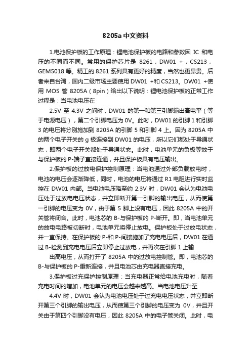
8205a中文资料1.电池保护板的工作原理:锂电池保护板的电路和参数因IC和电压的不同而不同。
常用的保护芯片是8261,DW01 +,CS213,GEM5018等。
精工的8261系列具有更好的精度,当然也更昂贵。
后者来自台湾,国内二级市场主要使用DW01 +和CS213。
DW01 +使用MOS管8205A(8pin)给出以下说明:锂电池保护板的正常工作过程是:当电池电压在2.5V至4.3V之间时,DW01的第一和第三引脚输出高电平(等于电源电压),第二个引脚电压为0V。
此时,DW01的引脚1和引脚3的电压将分别施加到8205A的引脚5和引脚4上。
因为8205A中的两个电子开关的g极连接到DW01的电压,所以它们都处于导通状态,即两个电子开关都处于导通状态。
此时,电池单元的负极等效于与保护板的P-端子直接连通,并且保护板具有电压输出。
2.保护板的过放电保护控制原理:当电池通过外部负载放电时,电池的电压会逐渐降低,同时,电池的电压将通过R1电阻进行实时监控在DW01内部。
当电池电压降至约2.3V时,DW01会认为电池电压处于过放电电压状态,并立即断开第一引脚的输出电压,从而使第一引脚的电压变为0V,由于第5脚上没有电压,因此8205A中的开关管将闭合。
此时,电池芯的B-与保护板的P-断开。
即,当电池单元的放电电路被切断时,电池单元将停止放电。
保护板处于过放电状态,并一直保持。
在保护板的P-和P-间接施加了充电电压后,DW01在通过B-检测到充电电压后立即停止过放电,并再次在引脚1上输出高电压,从而打开了8205A中的过放电控制管。
即,电池芯的B-与保护板的P-重新连接,并且电池芯由充电器直接充电。
3.保护板过充保护控制原理:当充电器正常给电池充电时,随着充电时间的增加,电池单元的电压会越来越高。
当电池电压升至4.4V时,DW01会认为电池电压处于过充电电压状态,并立即断开第三个引脚的输出电压,从而使第三个引脚的电压变为0V,并且开关由于第四个引脚没有电压,因此8205A中的电子管关闭。
8205PDF资料

U E D P R O D U C T R E F E R E N C E O N L Y Designed specifically to meet the requirement for extended opera-tion of battery-powered equipment such as cordless and cellular tele-phones, the A8205SLH voltage regulators offer the reduced dropout voltage and quiescent current essential for maximum battery life.Applicable also to palmtop computers and personal data assistants,these devices deliver a regulated output at up to 200 mA (transient),which is limited only by package power dissipation. Regulated output voltages of 2.7, 2.8, 3.0, 3.3, 3.6, 4.0, and 5.0 V are currently provided.Other voltages, down to 2.0 volts, are available on special order.A PMOS pass element provides a typical dropout voltage of only 75 mV at 100 mA of load current. The low dropout voltage permits deeper battery discharge before output regulation is lost. Quiescent current does not increase significantly as the dropout voltage is ap-proached, an ideal feature in standby/resume power systems where data integrity is crucial. Regulator accuracy and excellent temperature characteristics are provided by a bandgap reference. The A8205SLH includes an ENABLE input to give the designer complete control over power up, standby, or power down.These devices are supplied in a thermally enhanced 5-lead small-outline plastic package similar to the SOT-23, and fitting the SC-74A footprint. All devices are rated for operation over a temperature range of -20°C to +85°C.FEATURES AND BENEFITSI High Efficiency Provides Extended Battery Life I 75 mV Typical Dropout Voltage at I O = 100 mA I 55 µA Typical Quiescent Current Less Than 1 µA “Sleep” Current I Low Output NoiseI 200 mA Peak Output CurrentI Improved PSRR and Transient PerformanceAPPLICATIONSI Cordless and Cellular Telephones I Personal Data Assistants I Personal Communicators IPalmtop ComputersLOW-DROPOUT REGULATORS— HIGH EFFICIENCYData Sheet 27468.20Always order by complete part number, e.g., A8205SLH-xx , where “xx”is the required output voltage in tenths or “ADJ” for adjustable.8205PRELIMINARY INFORMATION(subject to change without notice)December 6, 19998205LOW-DROPOUTREGULATORS115 Northeast Cutoff, Box 15036Worcester, Massachusetts 01615-0036 (508) 853-5000Copyright © 1999, 2000 Allegro MicroSystems, Inc.A8205SLH Maximum Allowable Average Output Current* with device mounted on 2.24" x 2.24"(56.9 mm x 56.9 mm) solder-coated copper-clad board in still air.Allowable Total Average (10 ms) Output Current in Milliamperes with T J = 150°C, Duty Cycle = 100%†V I - V OT A 0.5 1.0 1.5 2.0 2.5 3.0 3.5 4.0* 4.5*25°C 20020020020020018916214212650°C 20020020020018215213011410170°C 200200200182145121104918185°C20020019714811898847466* Absolute maximum peak output current rating is 200 mA; absolute maximum input voltage is 7 V.† I O = (T J – T A )/([V I – V O ] R θJA x dc) = (150 – T A )/([V I – V O ] x 220 x 1.00)Output current rating can be increased (to 200 mA maximum) by additional heat sinking or reducing the duty cycle.8205LOW-DROPOUT REGULATORSELECTRICAL CHARACTERISTICS at T A = +25°C, V E = V I (unless otherwise noted).LimitsCharacteristic Symbol Test ConditionsMin.Typ.Max.UnitsOutput VoltageV O V I ≥ V O(nom) + 1 V, 1 mA ≤ I O ≤ 150 mA*,reference specified V O(nom)—0.0±1.5%Output Volt. Temp. Coeff.a VO V I = 6 V, I O = 10 mA, T J ≤ 125°C —40—ppm/°C Line Regulation ∆V O(∆VI)V O(nom) + 1 V ≤ V I ≤ 7 V, I O = 3 mA ——±1.5%Load Regulation∆V O(∆IO)V I = V O(nom) + 1 V, 1 mA ≤ I O ≤ 150 mA*——±1.5%V I = 7 V, 1 mA ≤ I O ≤ 150 mA*——±1.5%Dropout Voltage V I min - V OI O = 100 mA—75200mV Ground Terminal CurrentI GNDV I = V O(nom) + 1 V, I O = 1 mA —5565µA V I = V O(nom) + 1 V, I O = 150 mA*—5565µA V I = 7 V, I O = 1 mA —5565µA V I = 7 V, I O = 150 mA*—5565µA I QV I ≤ 7 V, V E ≤ 0.8 V, I O = 0 mA —— 1.0µA ENABLE Input VoltageV EH V I ≥ V O(nom) + 1 V, Output ON 2.0——V V ELV I ≥ V O(nom) + 1 V, Output OFF ——0.4V ENABLE Input Current I E V E = V I = 7 V——±1.0µA Internal Reference Voltage V REF — 1.26—V ADJUST Input Current I ADJ A8205SLH-ADJ only—0.10—µARejection RatioPSRRV I = V O(nom) + 1.5 V, V i = 100 mV,I O = 30 mA, f = 60 Hz—70—dB Output Noisee n10 Hz ≤ f ≤ 100 kHz, I O = 10 mA, C O = 10 µF —0.5—µV/√HzTypical values are at T A = +25°C and are given for circuit design information only.* Pulse test (≤20 ms). See previous page for duty cycle limitations.8205LOW-DROPOUTREGULATORS115 Northeast Cutoff, Box 15036Worcester, Massachusetts 01615-0036 (508) 853-5000APPLICATIONS INFORMATIONLinear regulators require input and output capacitors in order to maintain over-all loop stability. The recommended minimum value for the input capacitor is 0.1 µF. The output capacitor is the dominant pole that provides the high-frequency compensa-tion required for over-all regulator loop stability. These devices are stable with as little as 1 µF. However, to ensure stable operation under all conditions and capacitor types, the recom-mended minimum value is 4.7 µF. The output capacitor may be partially distributed through the load circuits. However, at least 1 µF should be connected at the regulator using the shortest and widest foil pattern possible.The A8205SLH-ADJ requires an external voltage divider to set up the desired regulated output voltage between 2.0 V and 6.8 V (V I ≤ 7 V). The two resistors are chosen such thatV O = 1.26 (R 1 + R 2)/R 2.The resistor values are usually as high as possible to maintain high circuit efficiency, but R 2 should be less than 300 k Ω.ENABLE(ACTIVE HIGH)INPUT (7.0 V MAX)Thermal ConsiderationsThese devices are intended to provide more than 150 mA of continuous current in a very small package. The table on page 2of this data sheet gives the maximum allowable average output current for a worst-case printed circuit design (R θJA = 220°C/W with a minimum footprint). Performance improvement is easily accomplished with the addition of 1 square inch of copper at terminal 2 (R θJA = 170°C/W).8205LOW-DROPOUTREGULATORSTHIS PAGE INTENTIONALLY LEFT BLANK8205LOW-DROPOUTREGULATORS115 Northeast Cutoff, Box 15036Worcester, Massachusetts 01615-0036 (508) 853-5000THIS PAGE INTENTIONALLY LEFT BLANK8205LOW-DROPOUT REGULATORSDimensions in Inches(for reference only)Dimensions in Millimeters(controlling dimensions)MINDwg. MA-011-5 mmNOTES: 1. Tolerances on package height and width represent allowable mold offsets.Dimensions given are measured at the widest point (parting line).2. Exact body and lead configuration at vendor’s option within limits shown.3. Height does not include mold gate flash.4. Where no tolerance is specified, dimension is nominal.MIN8205LOW-DROPOUTREGULATORS115 Northeast Cutoff, Box 15036Worcester, Massachusetts 01615-0036 (508) 853-5000The products described here are manufactured under one or more U.S. patents or U.S. patents pending.Allegro MicroSystems, Inc. reserves the right to make, from time to time, such departures from the detail specifications as may be required to permit improvements in the performance, reliability, ormanufacturability of its products. Before placing an order, the user is cautioned to verify that the information being relied upon is current.Allegro products are not authorized for use as critical components in life-support devices or systems without express written approval.The information included herein is believed to be accurate and reliable. However, Allegro MicroSystems, Inc. assumes no responsi-bility for its use; nor for any infringement of patents or other rights of third parties which may result from its use.。
平芯微8205A8TS,8205A6S最新规格书

GENERAL DESCRIPTIONFEATURESVDS = 20V,ID = 6ARDS(ON) < 27 mΩ @ VGS=4.5V RDS(ON) < 37 mΩ @ VGS=2.5VAbsolute Maximum Ratings (TA=25℃unless otherwise specified)ParameterSymbol RatingUnitDrain-Source Voltage V DS20 V Gate-Source Voltage V GS±12 V Drain Current-Continuous ID6 A Drain Current Pulsed(Note1)I DM25 A Maximum Power Dissipation P D1.5 W Storage Temperature Range T STG-55 To 150 ℃ Operating Junction Temperature Range T J -55 To 150 ℃ Thermal Resistance, Junction-to-Ambient(Note2)R θJA83℃/WG1S1S1D1/D2G2S2S2D1/D2D1D2G1G2S1S2 The 8205A is the highest performance trench N-ch MOSFETs with extreme high cell density, whichprovide excellent RDSON and gate charge for most of the small power switching and load switch applications. The meet the RoHS and Product requirement with full function reliability approved.S OT-23-6LS1G1D1/D2D1/D2S2G2TSSOP-8参考电路图,如:单节锂电池保护板开关MOS应用Fig.1 Switching Test CircuitFig.2 Switching WaveformsFig.3 Power DissipationFig.4Drain CurrentFig.5 Output Characteristics Fig.6 Drain-Source On-ResistanceVoutV INV tT J -Junction Temperature(℃)T J -Junction Temperature(℃)P D P o w e r (W )I D - D r a i n C u r r e n t (A )Vds Drain-Source Voltage (V)I D - Drain Current (A)R d s o n O n -R e s i s t a n c e (m Ω) I D - D r a i n C u r r e n t (A )Fig.7 Transfer CharacteristicsFig.8 Drain-Source On-ResistanceFigure 9 Rdson vs VgsFigure 10Capacitance vs VdsFig 11. Gate ChargeFig 12. Source- Drain Diode ForwardVgs Gate-Source Voltage (V)T JJunction Temperature ( - ℃ )V g s Gate-Source Voltage (V)Vds Drain-Source Voltage (V)Qg Gate Charge (nC)Vsd Source-Drain Voltage (V)Figure 13 Safe Operation AreaFigure 14 Normalized Maximum Transient Thermal ImpedanceVds Drain-Source Voltage (V)Square Wave Pluse Duration(sec)PACKAGE DESCRIPTIONTSSOP8。
- 1、下载文档前请自行甄别文档内容的完整性,平台不提供额外的编辑、内容补充、找答案等附加服务。
- 2、"仅部分预览"的文档,不可在线预览部分如存在完整性等问题,可反馈申请退款(可完整预览的文档不适用该条件!)。
- 3、如文档侵犯您的权益,请联系客服反馈,我们会尽快为您处理(人工客服工作时间:9:00-18:30)。
TXY8205
Dual N CHANNEL High Density Trench MOSFET
TYPE BV DSS R DS(ON)I D
25mΩ@VGS=4.5V6A
TXY8205 20V
40mΩ@VGS=2.5V5A
Green Product
PIN DESCRIPTION
FEATURES
High Density cell trench design for low Rds(on)
Rugged and reliable
Surface Mount package
Lead Free Available(Green Product)
ABSOLUTE MAXIMUM RATINGS
Unit Symbol Parameter Value
V DSS Drain-Source Voltage ( V GS=0V )20 V
V GSS Gate- source Voltage±12V V
I D (a) Drain Current (continuous) at T C = 25 ℃ 6 A
I D Drain Current (continuous) at T C = 100 ℃ 2.4 A
I DM (b) Drain Current (pulsed)24 A
Ptot Total Dissipation at T C = 25 ℃ 1.25 W
Temperature
Tstg Storage
- 55~175 ℃
Tj Max. Operating Junction Temperature
(a) Current limited by package
(b) Pulse width limited by safe operating area
THERMAL DATA
Rthj-amb Thermal Resistance Junction-ambient Max 100 ℃ / W
ELECTRICAL CHARACTERISTICS (T case = 25 ℃ unless otherwise specified)
OFF
Symbol
Parameter
Test Conditions
Min Typ Max Unit BV DSS Drain-source
Breakdown Voltage
I D = 250 uA , V GS = 0V
20
V
I DSS
Zero Gate Voltage Drain Current (V GS = 0V)
V DS = 16V 1 uA I GSS Current (V DS = 0V)
V GS =± 12V
±100
nA
ON
Symbol
Parameter
Test Conditions
Min Typ Max Unit V GS(th) Gate Threshold Voltage V DS = V GS , I D = 250uA 0.5 0.7 1.2 V V GS = 4.5V , I D =6A 23 25 m ΩR DS(on)
Static Drain-source On Resistance
V GS = 2.5V , I D =5A
34
40
m Ω
DYNAMIC
Symbol
Parameter
Test Conditions
Min
Typ
Max
Unit
Ciss Input Capacitance 595 PF Coss Output Capacitance 140 PF Crss Reverse Transfer Capacitance
V DS = 10V , f = 1 MHz , V GS=0V
125 PF
ELECTRICAL CHARACTERISTICS (continued)
SWITCHING ON
Symbol Parameter
Test Conditions
Min Typ Max Unit
td ( on )
Turn-on Delay Time
3.5
ns tr Rise Time V DD =10V , I D = 6A , Rg=3Ω V GS =4.5V
13.5 ns Qg
Total Gate Charge
21
nc
Qgs Gate-Source Charge 1.3 nc Qgd Gate-Drain Charge
V DD = 10V , I D =6 A , V GS = 4.5V 3.3 nc
SWITCHING OFF
Symbol Parameter
Test Conditions
Min Typ Max Unit td (off)
Turn-off Delay Time
32
ns tf Fall Time
V DD = 10V , I D =6A , Rg=3Ω V GS =4.5V
6.6
ns
SOURCE DRAIN DIODE
Symbol Parameter
Test Conditions
Min Typ Max Unit
IS
Continuous source-drain diode current
T C = 25℃
6 A Trr Body diode reverse recovery Time
14
nS
Qrr
Body diode reverse recovery charge
IF=6A , di/dt = 100A/us , Tj=25℃
5 nC
VSD
Forward On Voltage
ISD =1.0 A , V GS = 0V
0.78
1.2
V。