37PIN裸屏规格书
P460HVN01.0-1920×1080-700cd-20111101
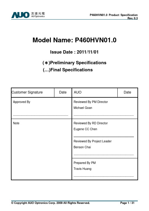
Model Name: P460HVN01.0Issue Date : 2011/11/01(*)Preliminary Specifications(…)Final SpecificationsCustomer Signature Date AUO DateApproved By_________________________________ Reviewed By PM DirectorMichael Goan____________________________________Reviewed By RD DirectorEugene CC Chen____________________________________ Reviewed By Project LeaderBenson Chai____________________________________NotePrepared By PMTravis Huang____________________________________ContentsNoCONTENTSRECORD OF REVISIONS1 GENERAL DESCRIPTION2 ABSOLUTE MAXIMUM RATINGS3 ELECTRICAL SPECIFICATION3-1 ELECTRIACL CHARACTERISTICS3-2 INTERFACE CONNECTIONS3-3 SIGNAL TIMING SPECIFICATION3-4 SIGNAL TIMING WAVEFORM3-5 COLOR INPUT DATA REFERENCE3-6 POWER SEQUENCE3-7 BACKLIGHT SPECIFICATION4 OPTICAL SPECIFICATION5 MECHANICAL CHARACTERISTICS5-1 PLACEMENT SUGGESTIONS6 RELIABILITY TEST ITEMS7 INTERNATIONAL STANDARD7-1 SAFETY7-2 EMC8 PACKING8-1 DEFINITION OF LABEL8-2 PACKING METHODS8-3 PALLET AND SHIPMENT INFORMATION9 PRECAUTION9-1 MOUNTING PRECAUTIONS9-2 OPERATING PRECAUTIONS9-3 ELECTROSTATIC DISCHARGE CONTROL9-4 PRECAUTIONS FOR STRONG LIGHT EXPOSURE9-5 STORAGE9-6 HANDLING PRECAUTIONS FOR PROTECT FILM9-7 OPERATING CONDITION IN PID APPLICATIONRecord of RevisionVersion Date Page Description0.0 2011/06/23 First preliminary spec sheet release0.1 2011/7/5 22 Front View Drawing Update23 Read View Drawing Update0.2 2011/07/25 4 Format change0.3 2011/11/01 4 Format change1. General DescriptionThis specification applies to the 46.0 inch Color TFT-LCD Module P460HVN01.0. This LCD module has a TFT active matrix type liquid crystal panel 1,920x1,080 pixels, and diagonal size of 46.0 inch. This module supports 1,920x1080 mode. Each pixel is divided into Red, Green and Blue sub-pixels or dots which are arranged in vertical stripes. Gray scale or the brightness of the sub-pixel color is determined with a 10-bit gray scale signal for each dot.The P460HVN01.0 has been designed to apply the 10-bit 2 channel LVDS interface method. The main feature of P460HVN01.0 would be high brightness, high contrast, wide viewing angle, high color saturation, super narrow bezel, direct LED backlight and high color depth.* General InformationItems Specification Unit NoteActive Screen Size 46.0 InchDisplay Area 1018.08(H) x 572.67(V) mmOutline Dimension 1026.68(H) x 578.27(V) x 37.5(D) mm 1Driver Element a-Si TFT active matrixDisplay Colors 10 bit (8bit+FRC), 1073.7M ColorsNumber of Pixels 1,920x1080 PixelPixel Pitch 0.176 (H) x 0.53(W) mmPixel Arrangement RGB vertical stripeDisplay Operation Mode Normally BlackDisplay Orientation Landscape/Portrait EnableSurface Treatment AG Haze = 11% Note:(1) Dmax: 54.2mm (Front bezel to Driver cover); Dmin: 37.5mm (Front bezel to Bezel back)2. Absoute Maximum RatingsThe followings are maximum values which, if exceeded, may cause faulty operation or damage to the unitItem Symbol Min Max Unit Conditions Logic/LCD Drive Voltage Vcc -0.3 14 [Volt] Note 1Input Voltage of Signal Vin -0.3 4 [Volt] Note 1Operating Temperature TOP 0 +50 [o C] Note 2Operating Humidity HOP 10 90 [%RH] Note 2Storage Temperature TST -20 +60 [o C] Note 2Storage Humidity HST 10 90 [%RH] Note 2Panel Surface Temperature PST 65 [o C] Note 3Note 1: Duration:50 msec.Note 2 : Maximum Wet-Bulb should be 39 and No condensation.℃The relative humidity must not exceed 90% non-condensing at temperatures of 40or less. At temperatures℃greater than 40, the wet bulb temperature must not exceed 39.℃℃Note 3: Surface temperature is measured at 50℃ Dry condition3. Electrical SpecificationThe P460HVN01.0 requires two power inputs. One is employed to power the LCD electronics and to drive the TFT array and liquid crystal. The second is employed for LED driver.3.1.1 Electrical CharacteristicsValueParameter SymbolMin. Typ. MaxUnit Note LCDPower Supply Input Voltage V DD10.8 12 13.2 V DCPower Supply Input Current I DD-- 0.9 1.08 A 1 Power Consumption P C-- 10.8 12.96 Watt 1 Inrush Current I RUSH- - 5.5 A 2 Permissible Ripple of Power Supply InputVoltage(for input power=12V)V RP-- -- V DD * 5% mV pk-pk 3 Input Differential Voltage ∣V ID∣200 400 600 mV DC 4Differential Input High ThresholdVoltageV TH+100 -- +300 mV DC 4Differential Input Low Threshold Voltage V TL-300 -- -100 mV DC4LVDSInterfaceInput Common Mode Voltage V ICM 1.1 1.25 1.4V DC4Input High Threshold VoltageV IH(High)2.7 --3.3 V DCCMOSInterfaceInput Low Threshold VoltageV IL(Low)0 -- 0.6 V DC7Backlight Power Consumption P BL-- 203 WLife Time(MTTF) -- 50000 -- 8 3.1.2 AC CharacteristicsValueParameter SymbolMin. Typ. MaxUnit Note Receiver Clock : SpreadSpectrum Modulation range Fclk_ssFclk-3%--Fclk+3%MHz 9Receiver Clock : SpreadSpectrum Modulation frequency Fss30--200KHz9LVDSInterfaceReceiver Data Input MarginFclk = 85 MHz Fclk = 65 MHz tRMG-0.4-0.5----0.40.5ns10Note :1. Test Condition:(1) V DD = 12.0V(2) Fv = Type Timing, 60Hz, 120Hz or Other (3) F CLK = Max freq. (4) Temperature = 25 ℃ (5) Test Pattern : White Pattern2. Measurement condition : Rising time = 400usDD3. Test Condition:(1) The measure point of V RP is in LCM side after connecting the System Board and LCM. (2) Under Max. Input current spec. condition.4. V ICM = 1.25VID |V IC G N 0VL V D S -L V D S5. Do not attach a conducting tape to lamp connecting wire. If the lamp wire attach to conducting tape,TFT-LCD Module have a low luminance and the inverter has abnormal action because leakage current occurs between lamp wire and conducting tape.6. The relative humidity must not exceed 80% non-condensing at temperatures of 40 or less. At℃temperatures greater than 40, the wet bulb temperature must not exceed 39. When operate at low ℃℃temperatures, the brightness of LED will drop and the life time of LED will be reduced.7. The measure points of V IH and V IL are in LCM side after connecting the System Board and LCM.8. The lifetime (MTTF) is defined as the time which luminance of the LED is 50% compared to its original value. [Operating condition: Continuous operating at Ta = 25±2℃]9. LVDS Receiver Clock SSCG (Spread spectrum clock generator) is defined as below figuresFclk Fclk__ss ss((max max))Fclk Fclk__ss ss((min min))Fclk10. Receiver Data Input MarginRatingParameterSymbol Min Type Max Unit Note Input Clock Frequency Fclk Fclk (min) -- Fclk (max) MHz T=1/Fclk Input Data Position0 tRIP1 -|tRMG| 0 |tRMG| ns Input Data Position1 tRIP0 T/7-|tRMG| T/7 T/7+|tRMG| ns Input Data Position2 tRIP6 2T/7-|tRMG| 2T/7 2T/7+|tRMG| ns Input Data Position3 tRIP5 3T/7-|tRMG| 3T/7 3T/7+|tRMG| ns Input Data Position4 tRIP4 4T/7-|tRMG| 4T/7 4T/7+|tRMG| ns Input Data Position5 tRIP3 5T/7-|tRMG| 5T/7 5T/7+|tRMG| ns Input Data Position6 tRIP26T/7-|tRMG|6T/76T/7+|tRMG|nsP460HVN01.0 Product SpecificationRev. 0.33.2Interface ConnectionsLCD connector : 187059-51221(Manufactured by P-TWO);PIN Symbol Description PIN Symbol Description1 VCC 12V Power Supply 27 RXEN1 LVDS Even pixel data input pair 1(-)2 VCC 12V Power Supply 28 RXEP1 LVDS Even pixel data input pair 1(+)3 VCC 12V Power Supply 29 RXEN2 LVDS Even pixel data input pair 2(-)4 VCC 12V Power Supply 30 RXEP2 LVDS Even pixel data input pair 2(+)5 VCC 12V Power Supply 31 GND GND6 GND GND 32 RXENCLK LVDS Even pixel clock input pair(-)7 GND GND 33 RXEPCLK LVDS Even pixel clock input pair(+)8 GND GND 34 GND GND9 GND GND 35 RXEN3 LVDS Even pixel data input pair 3(-)10 RXON0 LVDS Odd pixel data input pair 0(-) 36 RXEP3 LVDS Even pixel data input pair 3(+)11 RXOP0 LVDS Odd pixel data input pair 0(+) 37 RXEN4 LVDS Even pixel data input pair 4(-)12 RXON1 LVDS Odd pixel data input pair 1(-) 38 RXEP4 LVDS Even pixel data input pair 4(+)13 RXOP1 LVDS Odd pixel data input pair 1(+) 39 GND GND14 RXON2 LVDS Odd pixel data input pair 2(-) 40 NC No connected15 RXOP2 LVDS Odd pixel data input pair 2(+) 41 Reserved AUO Internal Use Only16 GND GND 42 NC No connected17 RXONCLK LVDS Odd pixel clock input pair(-) 43 NC No connected18 RXOPCLK LVDS Odd pixel clock input pair(+) 44 NC No connected19 GND GND20 RXON3 LVDS Odd pixel data input pair 3(-) 45 LVDSORDSelect LVDS data order:High or NC →NS, Low →JEIDA21 RXOP3 LVDS Odd pixel data input pair 3(+) 46 NC No connected22 RXON4 LVDS Odd pixel data input pair 4(-) 47 NC No connected23 RXOP4 LVDS Odd pixel data input pair 4(+) 48 NC No connected24 GND GND 49 Reserved AUO Internal Use Only25 RXEN0 LVDS Even pixel data input pair 0(-) 50 Reserved AUO Internal Use Only26 RXEP0 LVDS Even pixel data input pair 0(+) 51 Reserved AUO Internal Use OnlyNote 1: All GND (ground) pins should be connected together and should also be connected to the LCD’s metal frame.Note 2: All V DD (power input) pins should be connected together.Note 3: All NC (no connection) pins should be open without voltage input.P460HVN01.0 Product SpecificationRev. 0.3 LVDS Option = High/Open NSC lo cC H xC H xC H xC H xC H xC H xC H xC H xC H xC H xNote: x = 1, 2, 3, 4…C loC H xC H xC H xC H xC H xC H xC H xC H xC H xC H xNote: x = 1, 2, 3, 4…P460HVN01.0 Product Specification Rev. 0.33.3 Signal Timing SpecificationThis is the signal timing required at the input of the user connector. All of the interface signal timing should be satisfied with the following specifications for its proper operation.Timing Table (DE only Mode) Vertical Frequency Range (60Hz)Signal Item Period Vertical Section Active Blanking Period Horizontal Section Active Blanking Clock Vertical Frequency Horizontal Frequency Frequency Frequency Frequency Symbol Tv Tdisp (v) Tblk (v) Th Tdisp (h) Tblk (h) Fclk=1/Tclk Fv Fh 70 50 47 60 10 1030 Min. 1090 Typ. 1125 1080 45 1100 960 140 74.25 60 67.5 365 82 63 73 400 1325 Max 1480 Unit Th Th Th Tclk Tclk Tclk MHz Hz KHzNotes: (1) Display position is specific by the rise of DE signal only. Horizontal display position is specified by the rising edge of 1 DCLK after the rise of 1 DE, is displayed on the left edge of the screen. (2)Vertical display position is specified by the rise of DE after a “Low” level period equivalent to eight times of horizontal period. The 1 data corresponding to one horizontal line after the rise of 1 DE is displayed at the top line of screen. (3)If a period of DE “High” is less than 1920 DCLK or less than 1080 lines, the rest of the screen displays black. (4)The display position does not fit to the screen if a period of DE “High” and the effective data period do not synchronize with each other.st st st st© Copyright AUO Optronics Corp. 2009 All Rights Reserved.Page 11 / 31P460HVN01.0 Product Specification Rev. 0.3Tv Tblk(v) Th DE Tdisp(v) N L in eM pixelRGB DataInvalid DataLine NLine 1Line 2Line 3Line 4Line NInvalid DataCLK Tclk Th Tdisp(h) DE Tblk(h)CH1Pixel M-7Pixel M-5Pixel M-3Pixel M-1Invalid DataPixel 1Pixel 3Pixel 5Pixel 7Pixel 9Pixel 11Pixel M-5Pixel M-3Pixel M-1Invalid DataPixel 1Pixel 33.4 Signal Timing WaveformsCH2Pixel M-6Pixel M-4Pixel M-2Pixel MInvalid DataPixel 2Pixel 4Pixel 6Pixel 8Pixel 10Pixel 12Pixel M-4Pixel M-2Pixel MInvalid DataPixel 2Pixel 4© Copyright AUO Optronics Corp. 2009 All Rights Reserved.Page 12 / 31P460HVN01.0 Product Specification Rev. 0.33.5 Color Input Data ReferenceThe brightness of each primary color (red, green and blue) is based on the 10 bit gray scale data input for the color; the higher the binary input, the brighter the color. The table below provides a reference for color versus data input. COLOR DATA REFERENCE Input Color Data Color RED MSB LSB MSB GREEN LSB MSB BLUE LSBR9 R8 R7 R6 R5 R4 R3 R2 R1 R0 G9 G8 G7 G6 G5 G4 G3 G2 G1 G0 B9 B8 B7 B6 B5 B4 B3 B2 B1 B0 Black Red(1023) Green(1023) Basic Blue(1023) Color Cyan Magenta Yellow White RED(000) RED(001) R ---RED(1022) RED(1023) GREEN(000) GREEN(001) G ---GREEN(1022) 0 GREEN(1023) 0 BLUE(000) BLUE(001) B ---BLUE(1022) BLUE(1023) 0 0 0 0 0 0 0 0 0 0 0 0 0 0 0 0 0 0 0 0 0 0 0 0 0 0 0 0 0 0 0 0 0 0 0 0 0 0 0 0 1 1 1 1 1 1 1 1 1 0 1 1 1 1 1 1 1 1 1 1 0 0 0 0 0 0 0 0 0 0 0 0 0 0 0 0 0 0 0 0 0 0 0 0 0 0 0 0 0 0 0 0 0 0 0 0 0 0 1 1 0 0 1 1 0 0 1 1 0 0 1 1 0 0 1 1 0 0 1 1 0 0 1 1 0 0 1 1 0 0 1 1 0 0 0 1 0 0 0 0 0 0 0 0 0 0 0 0 0 0 0 0 0 0 0 0 0 0 0 0 0 0 0 0 0 0 0 0 0 0 0 0 0 0 0 0 0 1 1 1 0 0 1 1 0 0 1 1 0 0 1 1 0 0 1 1 0 0 1 1 0 0 1 1 0 0 1 1 0 0 1 1 0 0 0 1 0 0 0 0 0 0 0 0 0 0 0 0 0 0 0 0 0 0 0 0 0 0 0 0 0 0 0 0 0 0 0 0 0 0 0 0 0 0 0 0 0 1 0 0 0 0 0 0 0 0 0 0 0 0 0 0 0 0 0 0 0 0 0 0 0 0 0 0 0 0 0 0 0 0 0 0 0 0 0 0 0 0 0 1 0 0 0 1 1 1 0 0 0 1 0 0 0 1 1 1 0 0 0 1 0 0 0 1 1 1 0 0 0 1 0 0 0 1 1 1 0 0 0 1 0 0 0 1 1 1 0 0 0 1 0 0 0 1 1 1 0 0 0 1 0 0 0 1 1 1 0 0 0 1 0 0 0 1 1 1 0 0 0 1 0 0 0 1 1 1 0 0 0 1 0 0 0 1 1 1 0 1 0 0 1 0 1 0 1 1 0 0 0 0 1 0 1 0 1 1 0 0 0 0 1 0 1 0 1 1 0 0 0 0 1 0 1 0 1 1 0 0 0 0 1 0 1 0 1 1 0 0 0 0 1 0 1 0 1 1 0 0 0 0 1 0 1 0 1 1 0 0 0 0 1 0 1 0 1 1 0 0 0 0 1 0 1 0 1 1 0 0 0 0 1 0 1 0 1 1 0 0 0 0 0 0 0 0 0 0 0 0 0 0 0 0 0 0 0 0 0 0 0 0 0 0 0 0 0 0 0 0 1 1 1 1 1 1 1 1 1 1 1 1 1 1 1 1 1 1 1 1 1 1 1 1 1 1 1 1 1 1 0 0 0 0 0 0 0 0 0 0 1 1 1 1 1 1 1 1 1 1 0 0 0 0 0 0 0 0 0 0 0 0 0 0 0 0 0 0 0 0© Copyright AUO Optronics Corp. 2009 All Rights Reserved.Page 13 / 31P460HVN01.0 Product Specification Rev. 0.33.6 Power Sequence Power Sequence of LCD90% 90% 10% 10%Pow er Supply For LCD VD D (+ 12 V )G ND10%t1t2t5t6t7Interface Signal ( LV DS Data & CLK )G NDValid D atat3t4Backlight on / off control signal ( VBLO N )GNDt8t9CM O S Interface SignalG NDParameter t1 t2 t3 t4 t5 t6 t7 t8 t9Values Min. 0.4 0.1 450 0*1Type. -------------------Max. 30 50 --------*2Unit ms ms ms ms ms ms ms ms ms0 --500 10 0--50 ---Note: (1) t4=0 : concern for residual pattern before BLU turn off. (2) t6 : voltage of VDD must decay smoothly after power-off. (customer system decide this value)© Copyright AUO Optronics Corp. 2009 All Rights Reserved.Page 14 / 31P460HVN01.0 Product Specification Rev. 0.33.7 Backlight SpecificationThe backlight unit contains 220pcs LED.3.7.1 Electrical specificationSpec Item 1 2 3 4 Input Voltage Input Current Input Power Inrush Current Symbol VDDB IDDB PDDB IRUSH ON 5 On/Off control voltage VBLON OFF VDDB=24V 0 VDDB=24V MAX 7 Dimming Control Voltage V_DIM MIN 8 9 Dimming Control Current Internal Dimming Ratio External PWM Control Voltage External PWM Control Current I_DIM DIM_R MAX V_EPWM MIN I_EPWM D_EPWM F_EPWM HI 14 15 DET status signal Input Impedance DET LO Rin VDDB=24V VDDB=24V 0 300 0.8 VDC Kohm VDDB=24V VDDB=24V VDDB=24V VDDB=24V 0 5 140 180 0.8 2 100 240 mADC % Hz VDC VDDB=24V VDDB=24V VDDB=24V VDDB=24V 5 2 0 2 100 5.5 VDC 3 VDC mADC % 3.1 0.8 1.5 5.5 mA VDC Condition Min VDDB=24V VDDB=24V VDDB=24V 22.8 --2 Typ 24 8.49 203.8 Max 25.2 8.9 213.5 TBD 5.5 VDC VDC ADC W ADC 1 1 2 Unit Note6On/Off control currentIBLON101112 External PWM Duty ratio 13 External PWM FrequencyOpen CollectorNote 1 : Dimming ratio= 100% (MAX) Ta=25±5 , Turn on for 45minutes Note 2: Measurement condition Rising time = 20ms (VDDB : 10%~90%) and at dimming ration = 100% Note 3: Less than10% dimming control is functional well and no backlight shutdown happened(℃)© Copyright AUO Optronics Corp. 2009 All Rights Reserved.Page 15 / 31P460HVN01.0 Product Specification Rev. 0.33.7.2 Input Pin AssignmentLED driver board connector: CI0114M1HRL-NH (Cvilux)Pin 1 2 3 4 5 6 7 8 9 10 11Symbol VDDB VDDB VDDB VDDB VDDB BLGND BLGND BLGND BLGND BLGND DETDescription Operating Voltage Supply, +24V DC regulated Operating Voltage Supply, +24V DC regulated Operating Voltage Supply, +24V DC regulated Operating Voltage Supply, +24V DC regulated Operating Voltage Supply, +24V DC regulated Ground and Current Return Ground and Current Return Ground and Current Return Ground and Current Return Ground and Current Return BLU status detection: Normal : 0~0.8V ; Abnormal : Open collector BLU On-Off control: BL On : High/Open (2V~5.5V); BL off : Low (0~0.8V/GND) Internal PWM (0~3.3V for 10~100% Duty, open for 100%) < NC ; at External PWM mode> External PWM (5%~100% Duty, open for 100%) < NC ; at Internal PWM mode>12VBLON13 14VDIM PDIM© Copyright AUO Optronics Corp. 2009 All Rights Reserved.Page 16 / 31P460HVN01.0 Product Specification Rev. 0.3CI0112M1HRL-NHPin 1 2 3 4 5 6 7 8 9 10 11 12Symbol VDDB VDDB VDDB VDDB VDDB BLGND BLGND BLGND BLGND BLGND NC NCDescription Operating Voltage Supply, +24V DC regulated Operating Voltage Supply, +24V DC regulated Operating Voltage Supply, +24V DC regulated Operating Voltage Supply, +24V DC regulated Operating Voltage Supply, +24V DC regulated Ground and Current Return Ground and Current Return Ground and Current Return Ground and Current Return Ground and Current Return No connection No connection(Note*) IF External PWM function includes 5% dimming ratio. Judge condition as below: (1) Backlight module must be lighted ON normally. (2) All protection function must work normally. (3) Uniformity and flicker could NOT be guaranteed© Copyright AUO Optronics Corp. 2009 All Rights Reserved.Page 17 / 31P460HVN01.0 Product Specification Rev. 0.34. Optical SpecificationOptical characteristics are determined after the unit has been ‘ON’ and stable for approximately 45 minutes in a dark environment at 25° C while panel is placed in the default position. The default position is T-con side as the top side of panel. The value specified is at an approximate distance 50cm from the LCD surface at a viewing angle of φ and θ equal to 0° .Fig.1 presents additional information concerning the measurement equipment and method.SR3 or equivalentParameter Contrast Ratio Surface Luminance (White) Luminance Variation Response Time (G to G) Color Gamut Color Coordinates RedSymbol Min. CR LWH δWHITE(9P) Tγ NTSC 3200 560 ---Values Typ. 4000 700 -6.5 72 Max --1.33 --UnitNotes 1cd/m22 3Ms %4RX RY0.640 0.330 0.320 Typ.-0.03 0.620 0.150 0.050 0.280 0.290 5 Typ.+0.03GreenGX GYBlueBX BYWhiteWX WYViewing Angle x axis, right(φ=0° ) x axis, left(φ=180° ) y axis, up(φ=90° ) y axis, down (φ=270° ) θr θl θu θd ----89 89 89 89 ----degree degree degree degree© Copyright AUO Optronics Corp. 2009 All Rights Reserved.Page 18 / 31P460HVN01.0 Product Specification Rev. 0.3Note: 1. Contrast Ratio (CR) is defined mathematically as: Contrast Ratio= Surface Luminance of Lon5 Surface Luminance of Loff52. Surface luminance is luminance value at point 5 across the LCD surface 50cm from the surface with all pixels displaying white. From more information see FIG 2. When lamp current IH = 11mA. the luminance with all pixels displaying white at center 5 location. 3. The variation in surface luminance, δWHITE is defined (center of Screen) as: δWHITE(9P)= Maximum(Lon1, Lon2,…,Lon9)/ Minimum(Lon1, Lon2,…Lon9) 4. Response time T LWH=Lon5 where Lon5 isγ is the average time required for display transition by switching the input signal for fiveTarget 0%25% to 0% 50% to 0% 75% to 0% 100% to 0% 50% to 25% 75% to 25% 100% to 25% 75% to 50% 100% to 50% 100% to 75%luminance ratio (0%,25%,50%,75%,100% brightness matrix) and is based on Fv=60Hz to optimize.Measured Response Time 0% 25% Start 50% 75% 100% 25%0% to 25%50%0% to 50% 25% to 50%75%0% to 75% 25% to 75% 50% to 75%100%0% to 100% 25% to 100% 50% to 100% 75% to 100%4. Viewing angle is the angle at which the contrast ratio is greater than 10. The angles are determined for the horizontal or x axis and the vertical or y axis with respect to the z axis which is normal to the LCD surface. For more information see FIG4.FIG. 2 LuminanceVH/2123456H789H/6 V/6 V/2© Copyright AUO Optronics Corp. 2009 All Rights Reserved.Page 19 / 31P460HVN01.0 Product Specification Rev. 0.3FIG.3 Response Time The response time is defined as the following figure and shall be measured by switching the input signal for “any level of gray(bright) “ and “any level of gray(dark)”. Any level of gray (Bright) Any level of gray (Dark) Any level of gray (Bright)0%, 25%, 50%, 75%, 100%0%, 25%, 50%, 75%, 100%FIG.4 Viewing Angle© Copyright AUO Optronics Corp. 2009 All Rights Reserved.Photodetector Output0%, 25%, 50%, 75%, 100%TimeT γ (F)T γ (R)Page 20 / 315. Mechanical CharacteristicsThe contents provide general mechanical characteristics for the model P546HW04 V0. In addition the figures in the next page are detailed mechanical drawing of the LCD.Horizontal (typ.) 1026.68 mmVertical (typ.) 578.27mmOutline DimensionDepth (typ.) 37.5 mmHorizontal (typ.) 1018.68 mmBezel Opening AreaVertical (typ.) 573.27 mmHorizontal 1018.08 mmActive Display AreaVertical 572.67 mmWeight TBD5.1 Placement suggestions:The Suggestion placement is as following:1. Landscape mode: The default placement is T-Con Side as the top side.2. Portrait mode: The default placement is T-Con side has to be placed in the right side via viewing fromthe front.Landscape (Front view) Portrait (Front view)Front ViewBack View6. Reliability Test Items (TBD)Test Item Q’ty Condition1 High temperature storage test 3 60,℃500hrs2 Low temperature storage test3 -20,℃500hrs3 High temperature operation test 3 50,℃500hrs4 Low temperature operation test 3 -5,℃500hrs5 Vibration test (non-operation) 3 Wave form: randomVibration level: 1.0G RMS Bandwidth: 10-300Hz, Duration: X, Y, Z 10min per axes X,Y,Z : Horizontal, face up6 Shock test (non-operation) 3 Shock level: 30GWaveform: half since wave, 11ms Direction: ±X, ±Y, ±Z, One time each direction7 Vibration test (With carton) 1 (PKG) Random wave (1.05G RMS, 10-200Hz) 10mins per each X,Y,Z axes8 Drop test (With carton) 1 (PKG) Surround four flats drop height:15 cm Bottom flat drop height:25.4 cm twice (ASTMD4169)7. International Standard7.1 Safety(1) UL60065,2003, Underwriters Laboratories, Inc. (AUO file number : E204356)Audio, video and similar electronic apparatus, safety requirement(2) UL60950-1,2003, Underwriters Laboratories, (AUO file number : E204356)Standard for safety of information technology equipment including electrical business equipment(3) EN60065(4) EN60950(5) IEC 60065, European Committee for Electro technical Standardization (CENELEC)Audio, video and similar electronic apparatus, safety requirement(6) IEC 60950-1:European Committee for Electrotechnical Standardization (CENELEC)European Standard for safety of information technology equipment including electrical businessequipment7.2 EMC(1) ANSI C63.4 “Methods of Measurement of Radio-Noise Emissions from Low-Voltage Electrical andElectrical Equipment in the Range of 9kHz to 40GHz. “American National standards Institute(ANSI), 1992(2) C.I.S.P.R “Limits and Methods of Measurement of Radio Interface Characteristics of InformationTechnology Equipment.” International Special committee on Radio Interference.(3) EN 55022 “Limits and Methods of Measurement of Radio Interface Characteristics of InformationTechnology Equipment.” European Committee for Electrotechnical Standardization. (CENELEC), 19988. Packing (TBD)8-1 DEFINITION OF LABEL: A. Panel Label:*xxxxxxxxxxxx-xxxx*Green mark description(1) For Pb Free Product, AUO will addfor identification.(2) For RoHs compatible products, AUO will add RoHS for identification.Note: The green Mark will be present only when the green documents have been ready by AUO internal green team. (definition of green design follows the AUO green design checklist.)B. Carton Label: (TBD)Panel Unique ID AUO Internal Use8-2 PACKING METHODS: (TBD)1pcs Module/ESD Bag8-3 Pallet and Shipment Information (TBD)SpecificationItemQty. Dimension (mm) Weight (kg)Packing Remark 1 Packing BOX 3 pcs/box 1305(L)*383(W)*800 (H) 75 2 Pallet11315(L)*1150(W)*132(H)203 Boxes per Pallet 3 boxes/pallet4 Panels per Pallet9 pcs/palletPallet after packing 9 pcs1315(L)*1150(W)*932(H)2459. PRECAUTIONSPlease pay attention to the followings when you use this TFT LCD module.9-1 MOUNTING PRECAUTIONS(1) You must mount a module using holes arranged in four corners or four sides.(2) You should consider the mounting structure so that uneven force (ex. twisted stress) is not appliedto module. And the case on which a module is mounted should have sufficient strength so thatexternal force is not transmitted directly to the module.(3) Please attach the surface transparent protective plate to the surface in order to protect the polarizer.Transparent protective plate should have sufficient strength in order to the resist external force.(4) You should adopt radiation structure to satisfy the temperature specification.(5) Acetic acid type and chlorine type materials for the cover case are not desirable because the formergenerates corrosive gas of attacking the polarizer at high temperature and the latter cause circuitbroken by electro-chemical reaction.(6) Do not touch, push or rub the exposed polarizer with glass, tweezers or anything harder than HBpencil lead. And please do not rub with dust clothes with chemical treatment. Do not touch thesurface of polarizer for bare hand or greasy cloth. (Some cosmetics are detrimental to the polarizer.)(7) When the surface becomes dusty, please wipe gently with absorbent cotton or other soft materialslike chamois soaks with petroleum benzene. Normal-hexane is recommended for cleaning theadhesives used to attach front/ rear polarizer. Do not use acetone, toluene and alcohol becausethey cause chemical damage to the polarizer.(8) Wipe off saliva or water drops as soon as possible. Their long time contact with polarizer causesdeformations and color fading.(9) Do not open the case because inside circuits do not have sufficient strength.9-2 OPERATING PRECAUTIONS(1) The device listed in the product specification sheets was designed and manufactured for TVapplication(2) The spike noise causes the mis-operation of circuits. It should be lower than following voltage:V=±200mV(Over and under shoot voltage)(3) Response time depends on the temperature. (In lower temperature, it becomes longer..)(4) Brightness of LED depends on the temperature. (In lower temperature, it becomes lower.) And inlower temperature, response time (required time that brightness is stable after turned on) becomeslonger.(5) Be careful for condensation at sudden temperature change. Condensation makes damage topolarizer or electrical contacted parts. And after fading condensation, smear or spot will occur.(6) When fixed patterns are displayed for a long time, remnant image is likely to occur.。
易欣达7寸数字京东方屏规格书
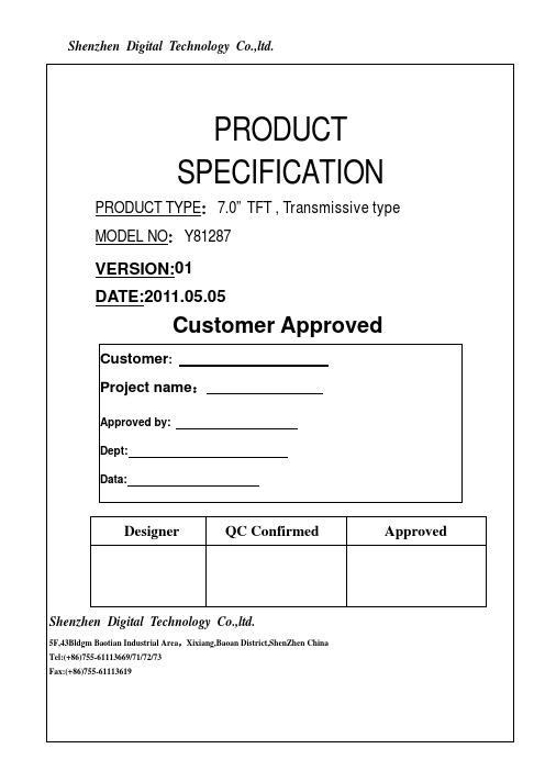
Shenzhen Digital Technology Co.,ltd.PRODUCTSPECIFICATIONPRODUCT TYPE:7.0” TFT , Transmissive typeMODEL NO:Y81287VERSION:01DATE:2011.05.05Customer ApprovedCustomer:Project name:Approved by:Dept:Data:Designer QC Confirmed ApprovedShenzhen Digital Technology Co.,ltd.5F,43Bldgm Baotian Industrial Area,Xixiang,Baoan District,ShenZhen ChinaTel:(+86)755-61113669/71/72/73Fax:(+86)755-61113619RECORDS OF REVISIONDESCRIPTIONS DATE Version REVISEDISSUE2011.05.05 01FIRST深圳市德智欣科技有限公司CONTENTS1. GENERAL DESCRIPTION - - - - - - - - - - - - - - - - - - - - - - - - - -2. MECHANICAL SPECIFICATIONS - - - - - - - - - - - - - - - - -- - - - - - - -3. OUTLINE DIMENSIONS - - - - - - - - - - - - - - - - - - - - -4. INTERFACE ASSIGNMENT - - - - - - - - - - - - - - - - - - - - - - - - --------5. TIMING CHARACTERISTICS - - - - - - - - - - - - - - - - - - - - - - - ------------------------------------------------6. RESETTIMINGCHARACTERISTICS7. POWER ON/OFF SEQUENCE - - - - - - - - - - - - - - - - - - - - - - - - - - -8. INSTRUCTION TABLE - - - - - - - - - - - - - - - - - - - - - - - - - - -9. ELECTRICAL CHARACTERISTICS - - - - - - - - - - - - - - - - - - - - -10. LED BACKLIGHT CHARACTERISTICS - - - - - - - - - - - - - - - - - - -11. OPTICAL CHARACTERISTICS - - - - - - - - - - - - - - - - - - - - - - - - - -Condition -----------------------------------------------------------12. Reliability13. Inspection Standards ----------------------------------------------------14. Precaution - - - - - - - - - - - - - - - - - - - - - - - -深圳市德智欣科技有限公司1.GENERAL DESCRIPTIONThis LCM Y81287 is a 800 x 3RGB x 480 dots matrix 7.0 ”TFT LCD module. It has a TFTpanel,composed of 1200 -channel source driver and 960-channel gate driver.2. MECHANICAL SPECIFICATIONSUNIT Item Contents LCD Type 7.0” TFT-LCD, TransmissiveOutline Dimension 100(W)x164.9(H)x3.4(T) mmActive Area 85.92(W) x151.68(H) mmViewing direction 6 O’CLOCK ---Source HX8664BDriver ICGate IC HX8264DDisplay Color 16MNumber of Dots 800(RGB)x480 DotsDot Pitch (H×V)0.0642(W) x 0.1790(H) mmAssy Type COG+FPC+BL ---BACKLIGHT WHITE LED Backlight -Interface24 bit interfaceWEIGHT TBD g深圳市德智欣科技有限公司4. INTERFACE ASSIGNMENTPIN NO. SYMBOL1 Power for LED backlighr (Anode) LEDA2 Power for LED backlighr (Anode) LEDA3 Power for LED backlighr (Cathode) LEDK4 Power for LED backlighr (Cathode) LEDKground GND5 Powervoltage VCOM6 Common7 Power for Digital Circuit DVDDmodeselect MODE8 DE/SYNC9 Data input Enable DE10 Vertical Sync Input VS11 Horizontal Sync Input HS12~19 Blue data B7~B020~27 Green data G7~G028~35 Red data R7~R036 Power ground GND37 Sample clock DCLK38 Power ground GND39 Left / right selection L/R40 Up/down selection U/D41 Gate NO Voltage VGH42 Gate OFF Voltage VGL43 Power for Analog Circuit A VDD44 Global reser pin RESET45 No connection NC46 Common Voltage VCOM47 Dithering function DITHB48 Power ground GND49 No connection NC50 No connection NC深圳市德智欣科技有限公司5.TIMING CHARACTERISTICS深圳市德智欣科技有限公司6.RESET TIMING CHARACTERISTICS深圳市德智欣科技有限公司7. POWER ON/OFF SEQUENCE深圳市德智欣科技有限公司8. HX8664B&HX8264D INSTRUCTION TABLE9. ELECTRICAL CHARACTERISTICS深圳市德智欣科技有限公司深圳市德智欣科技有限公司12. Reliability Condition13.Inspection Standards 13.1 Major DefectItem NoItems to be inspected Inspection Standard Classification of defects13.1.1 Allfunctional defects1)No display2) Display abnormally3) Missing vertical, horizontal segment 4) Short circuit5)Back-light no lighting flickering and abnormal lighting.13.1.2 Missing Missing component13.1.3 OutlinedimensionOverall outline dimension beyond the drawing is not allowed.Major13.2 Cosmetic defectItem No Item ConditionRemark1 High temperatureOperating 70°C ±2°C for 240 hours2 Low temperatureOperating -20°C ±2°C for 240 hours3 High temperatureStorage 80°C ±2°C for 240 hours4 Low temperatureStorage -30°C ±2°C for 240hours5High temperature & humidity Storage50℃±5°C , 90%RH, 120 hours 6Thermal Shock Storage (No operation)-20℃ , 30min.<=> 70℃ , 30min.10 Cycles7 ESD test-8 Vibration test 10 => 55 =>10 Hz, within 1 minute;Amplitude:1.5mm.15 minutes for each Direction ( X,Y ,Z ) 9 Drop testPacked, 100CM free fall6 sides, 1 corner, 3edgesNO DEFECT IN DISPLAYING AND OPERATIONAL FUNCTION深圳市德智欣科技有限公司(i) chips on cornerX Y Z ≤2.0≤SDisregardNotes:S=contact pad lengthChips on the corner of terminal shall not be allowed to extend intothe ITO pad or expose perimeter seal. Minor(ii)Usual surface cracksX Y Z≤3.0<Inner border line of the seal DisregardMinor13.3.1Glass defect(iii)CrackCracks tend to break are not allowed.Major13.3.2 Partsalignment1) Not allow IC and FPC/heat-seal lead width is more than 50 %beyond lead pattern.2) Not allow chip or solder component is off center more than 50 % of the pad outline. 13.3.3 SMTAccording to the <Acceptability of electronic assemblies>IPC-A-610C class 2 standard. Component missing or function defect are Major defect, the others are Minor defect.Major14. Precaution14.1 Handling(1) Protect the panel from static, it may cause damage to the CMOS Gate Array IC.(2) Use fingerstalls with soft gloves in order to keep display clean during the incominginspection and assembly process.(3) If the liquid crystal material leaks from the panel, it should be kept away from theeyes or mouth. In case of contact with hands, legs or clothes, it must be washedaway thoroughly with soap.(4) The desirable cleaners are water, IPA (Isopropyl Alcohol) or Hexane. Don’t useKetone type materials (ex. Acetone), Ethyl alcohol, Toluene, Ethyl acid or Methylchloride. It might permanent damage to the polarizer due to chemical reaction.(5) Pins of I/F connector shall not be touched directly with bare hands.(6) Refrain from strong mechanical shock and / or any force to the panel. In addition todamage, this may cause improper operation or damage to the panel.(7) Note that polarizers are very fragile and could be easily damaged. Do not press orscratch the surface harder than a B pencil lead.(8) Wipe off water droplets or oil immediately. If you leave the droplets for a long time,staining and discoloration may occur.(9) If the surface of the polarizer is dirty, clean it using some absorbent cotton or soft cloth.14.2 Storage(1) Do not leave the panel in high temperature, and high humidity for a long time. It ishighly recommended to store the panel with temperature from 0 to 35℃ andrelative humidity of less than 70%.(2) The panel shall be stored in a dark place. It is prohibited to apply sunlight orfluorescent light during the store.14.3 Operation(1) The LCD shall be operated within the limits specified. Operation at values outside ofthese limits may shorten life, and/or harm display images.(2) Do not exceed the absolute maximum rating value. (the supply voltage variation,Input voltage variation in part contents and environmental temperature and so on).Otherwise the panel may be damaged.(3) If the panel displays the same pattern continuously for a long period of time, it canbe the situation when the image” Sticks” to the screen.深圳市德智欣科技有限公司。
3.5寸液晶屏规格书SGC035COM—54PIN
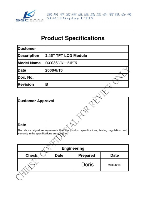
Product SpecificationsCustomerDescription 3.45” TFT LCD ModuleModel Name SGC035COM—54PINDate 2008/6/13Doc. No.Revision BCustomer ApprovalDateThe above signature represents that the product specifications, testing regulation, and warranty in the specifications are acceptedEngineeringCheck Date Prepared DateDoris2008/6/13CONTENTSNo. ITEM PAGE0 RECORD OF REVISION 31 SUMMARY 42 FEATURES 43 GENERAL SPECIFICATIONS 44 ABSOLUTE MAXIMUM RATINGS 45 ELECTRICAL CHARACTERISTICS 56 DC CHARATERISTICS 67 AC CHARACTERISTICS 6~108 OPTICAL CHARATERISTIC 119 TOUCH PANEL 14~1510 INTERFACE 16~1911 BLOCK DIAGRAM 2012 QUALITY ASSURANCE 2113 OUTLINE DRAWING 2214 PACKAGE INFORMATION 2315 PRECAUTIONS 24~26RECORD OF REVISIONSRevision Date Page DescriptionA 2008/2/12 all New CreationB 2008/6/13 18 LCM PIN Definition1. SUMMARYThis technical specification applies to 3.45“color TFT-LCD panel. The 3.45“ color TFT-LCD panel is designed for GPS, camcorder, digital camera application and other electronic products which require high quality flat panel displays. This module follows RoHS.2. FEATURESHigh Resolution: 230,400 Dots (320 RGB x 240). SGC 035COM—54PIN is atransmissive type color active matrix liquid crystal display (LCD) which uses amorphous thin film transistor (TFT) asswitching devices. This product is composed of a TFT LCD panel, driver ICs, FPC, backlight unit and touch panel.,3. GENERAL SPECIFICATIONSParameter Specifications Unit Screen size 3.45(Diagonal) InchDisplay Format 320 RGB x 240 DotActive area 70.08(H) x 52.56(V) mmDot size 73x 219 umPixel Configuration RGB-Stripe Outline dimension 76.9(W) x 63.9(H) x 3.3(D) mm Display Mode Normally white/Transmissive Surface Treatment Haze 20% Display Garmut NTSC 60% Input Interface Digital 24-bit RGB/SERIALRGB/CCIR656/CCIR601Weight (31) g View Angle direction 6 o’clockOperation -20~70 ℃Temperature RangeStorage -30~80 ℃4. ABSOLUTE MAXIMUM RATINGSItem Symbol Condition Min. Max. Unit Remark Power Voltage DVDD,AVDD GND=0 -0.3 5.0 V Input SignalVoltage V in GND=0 -0.3 VDD+0.3 VNOTE Logic OutputVoltageV OUT GND=0 -0.3 VDD+0.3 V NOTENote: Device is subject to be damaged permanently if stresses beyond those absolute maximum ratings listed above1. Temp. ≤ 60℃, 90% RH MAX.Temp. > 60℃, Absolute humidity shall be less than 90% RH at 60℃2.5. ELECTRICAL CHARACTERISTICS 5.1. Operating conditions:Parameter SymbolRatingMin. Typ. Max.Unit ConditionPower Voltage VCC 3.0 3.3 3.6 V Digital Operation CurrentIcc 8.6 mA Gate On Power VGH 14 15 18 V Gate Off Power VGL -11-10 -8V Vcom High Voltage VcomH 3.7 V Note1 Vcom low VoltageVcomL-1.6VNote1Vcom level max VcomA 6 VNote1. VcomH& VcomL :Adjust the color with gamma data. Vp-p should be higher then4V.(Option 5V)Note: Please power on following the sequence VCC Æ VDD5.2 LED driving conditionsParameter Symbol Min. Typ. Max. Unit Remark LED current- 20 - m A Power Consumption - 400 420 mW LED voltage VBL+ 18.619.8 21 V Note 1 LED Life Time - (50,000)- - HrNote 2,3Note 1 : There are 1 Groups LEDILEDNote 2 : Ta = 25℃Note 3 : Brightess to be decreased to 50% of the initial value深圳宏辉成液晶显示有限公司/6. DC CHARATERISTICSParameter SymbolRatingUnit Condition Min. Typ. Max.Low level input voltage V IL 0-0.3VCCVHight level input voltage V IH0.7VCC-VCC V7. AC CHARATERISTICSDigital Parallal RGB interfaceSignal Item Symbol Min Typ Max UnitFrequency Tosc - 156 - ns Dclk High Time Tch - 78 - nsLow Time Tcl - 78 - nsDataSetup Time Tsu 12 - - nsHold Time Thd 12 - - nsPeriod TH - 408 - Tosc Pulse Width THS 5 30 - ToscHsyncBack-Porch Thb 38 ToscDisplay Period TEP - 320 - ToscHsync-den time THE 36 68 88 TsocFront-Porch Thf - 20 - ToscPeriod Tv - 262 - THPulse Width Tvs 1 3 5 TH Vsync Back-Porch Tvb - 15 - TH Display Period Tvd - 240 - THFront-Porch Tvf 2 4 - TH1. Thp + Thb = 68, the user is make up by yourself.2. Tv = Tvs + Tvb + Tvd + Tvf , the user is make up by yourself.3.When SYNC mode is used,1st data start from 68th Dclk after Hsync fallingDigital Serial RGB interfaceSignal Item Symbol Min Typ Max Unit Frequency Tosc - 52 - ns Dclk High Time Tch - 78 - ns Low Time Tcl - 78 - nsData Setup Time Tsu 12 - - nsHold Time Thd 12 - - nsPeriod TH - 1224 - Tosc Pulse Width THS 5 90 - ToscHsyncBack-Porch Thb 114 ToscDisplay Period TEP - 960 - Tosc Hsync-den time THE 108 204 264Front-Porch Thf - 60 - ToscPeriod Tv - 262 - THPulse Width Tvs 1 3 5 THVsync Back-Porch Tvb - 15 - THDisplay Period Tvd - 240 - THFront-Porch Tvf 2 4 - TH Note: 1. Thp + Thb = 204, the user is make up by yourself.2. Tv = Tvs + Tvb + Tvd + Tvf , the user is make up by yourself.3. When SYNC mode is used,1st data start from 204th Dclk after Hsync fallinCCIR601/656 InterfaceSignalData Setup Time Tsu 12 - - ns Hold Time Thd 12 - - ns深圳宏辉成液晶显示有限公司/[_//f+--------------------H " "'= 1560--------------------+jInvalid Data Inva l i d Da t a018,0"'=DOTCLK In va li d DataIn v a l i d Data]---...t--f------------H018, =1440-------------+jslrL//RR[7:0]In va lid DataIn va l i d Dataf---- t.<sP = HBP[6:0]'4+STH[1:0'1-- *. - ----------- IH0,se = 128--- --- ----.!Figure1 CCIR601 Horizontal Timing深圳宏辉成液晶显示有限公司 /手机 : 133 166 766 58 MSN: lcd.sales@ QQ:1378107648Doc. No.SEL[2:0] = 100- 111, NTSCVSYNC HSYNCRR[7:0]tveP = VBP[6:0]DL1DL2DL3IDL2391DL240I---ODD Field VSYNCEVEN FieldHSYNCRR[7:0]tvsP= VBP[6:0] + 1·IODD FieldI IDL1DL2DL3IDL2391DL240ISEL[2:0] = 100- 111, PAL, PALM=OEVEN VSYNCHSYNCRR[7:0]tvsP= VBP[6:0]DL1DL2DL3IDL2791DL280IODD Field VSYNCEVEN Fi l eHSYNCRR[7:0]tvsP= VBP[6:0] + 1·IODD FieldI IDL1DL2DL3IDL2791DL280ISEL[2:0] = 100 - 111, PAL, PALM=1EVEN VSYNCHSYNCRR[7:0]tveP= VBP[6:0]DL1DL2DL3IDL2871DL288 1ODD Field VSYNCEVEN Fi l eHSYNCI深圳宏辉成液晶显示有限公司 /手机 : 133 166 766 58 MSN: lcd.sales@ QQ:1378107648IRR[7:0]lvsP= VBP[6 0] + 1·IDL1DL2DL3IDL287 1DL288 1Figure1CCIR601 Vertical Timing深圳宏辉成液晶显示有限公司 /手机 : 133 166 766 58 MSN: lcd.sales@ QQ:1378107648Figure2 CCIR656 Horizontal Timing深圳宏辉成液晶显示有限公司 /手机 : 133 166 766 58 MSN: lcd.sales@ QQ:1378107648Figure2 CCIR656 Vertical Timing深圳宏辉成液晶显示有限公司 /手机 : 133 166 766 58 MSN: lcd.sales@ QQ:1378107648Figure 3Digital RGB NTSC mode Vertical Data Format for 262THH cycle = 1224tHBP = 204HDISP = 960t HFP = 60DOTCLKHSYNCPixel DataDumm yD0D1----------D 957 D 958 D 959Dum mya ) Horizontal Data Transaction Tim ing V cycle = 262 Lines t VBP = 18VSYNC VDISP = 240 Lines t VFP = 4HSYNC Line 0 b ) Vertical Data Transaction Tim ing Line 239深圳宏辉成液晶显示有限公司 /手机 : 133 166 766 58 MSN: lcd.sales@ QQ:1378107648Figure 3 Data Transaction Timing in Serial RGB (8 bit) Interface (SYNC Mode)深圳宏辉成液晶显示有限公司 /手机 : 133 166 766 58 MSN: lcd.sales@ QQ:1378107648Figure3 Data Transaction Timing in Serial RGB (8 bit) Interface (DE Mode)深圳宏辉成液晶显示有限公司 /手机 : 133 166 766 58 MSN: lcd.sales@ QQ:1378107648Figure3Data Transaction Timing in Parallel RGB (24 bit) Interface (SYNC Mode)深圳宏辉成液晶显示有限公司 /手机 : 133 166 766 58 MSN: lcd.sales@ QQ:1378107648Figure4 Data Transaction Timing in Parallel RGB (24 bit) Interface (DE Mode)7.1.1 Standby ON/OFF Control LQ35NC211 has a power ON/OFF sequence control function. When STB pin is pulled L,blank data is outputted for 5-frames first, form the falling edge of the following VSYNC signal. The blank data would be gray level 255 for normally white LC.Figure5 Standby ON/OFF Control 7.1.2 Clock and Sync waveforms深圳宏辉成液晶显示有限公司 /手机 : 133 166 766 58 MSN: lcd.sales@ QQ:1378107648Figure6 CLK and IHS timing waveformTV FTC LTH B7.2 Reset Timing ChartThe RESET input must be held at least 1ms after power is stable8. OPTICAL CHARATERISTICTa=25±2℃, ILED=20mA Item Symbol Condition Min. Typ. Max. Unit Remark Response timeTr θ=0°、Φ=0°Tf- 10 ms- 15 msNote 3,5 Contrast ratio CRAt optimizedviewing angle300 400 - - Note 4,5 Color ChromaticityWhiteRedGreenBlueWxθ=0°、Φ=0WyRxθ=0°、Φ=0RyGxθ=0°、Φ=0GyBxθ=0°、Φ=0By(0.26) (0.31) (0.36) Note 2,6,7(0.28) (0.33) (0.38)Hor.ΘR(50) (60)Viewing angleΘL CR≧10(50) (60)Deg. Note 1Ver.ΦT(40) (50)ΦB(45) (55)Brightness - - 180 200 - cd/m2Center ofdisplayTa=25±2℃, I L=20mANote 1: Definition of viewing angle rangeFig. 8-1 Definition of viewing angleNote 2: Test equipment setup:After stabilizing and leaving the panel alone at a driven temperature for 10 minutes, the measurement should be executed. Measurement should be executed in a stable, windless, and dark room. Optical specifications are measured by Topcon BM-7 luminance meter 1.0° field of view at a distance of 50cm and normal direction.Fig. 8-2 Optical measurement system setupNote 3: Definition of Response time:The response time is defined as the LCD optical switching time interval between “White” state and“Black” state. Rise time, Tr, is the time between photo detector output intensity changed from 90﹪to 10﹪. And fall time, Tf, is the time between photo detector output intensity changedfrom10﹪to 90﹪.Note 4: Definition of contrast ratio:The contrast ratio is defined as the following expression.Contrast ratio (CR)= Luminance measured when LCD on the “White” stateLuminance measured when LCD on the “Black” stateNote 5: White Vi = V i50 ± 1.5VBlack Vi = Vi50 ± 2.0V“±” means that the analog input signal swings in phase with VCOM signal. “±” means that the analog input signal swings out of phase with VCOM signal.The 100% transmission is defined as the transmission of LCD panel when all the input terminals of module are electrically opened.Note 6: Definition of color chromaticity (CIE 1931)Color coordinates measured at the center point of LCDNote 7: Measured at the center area of the panel when all the input terminals of LCD panel are electrically opened.Brightness (min)Note 8 : Uniformity (U) = x 100%Brightness (max)9. TOUCH PANELNA10. INTERFACE10.1. LCM PIN DefinitionPin Symbol I/O Function Remark1 LED- I Backlight LED Ground2 LED- I Backlight LED Ground3 LED+ I Backlight LED Power4 LED+ I Backlight LED Power5 Y1 I Top electrode ,6 X1 I Right electrode7 NC Not Use8 /RESET - Hardware Reset9 SPENA I SPI Interface Data Enable Signal Note 310 SPCLK I SPI Interface Data Clock Note 311 SPDAT I SPI Interface Data Note 312 B0 I Blue Data Bit 013 B1 I Blue Data Bit 114 B2 I Blue Data Bit 215 B3 I Blue Data Bit 316 B4 I Blue Data Bit 417 B5 I Blue Data Bit 518 B6 I Blue Data Bit 619 B7 I Blue Data Bit 720 G0 I Green Data Bit021 G1 I Green Data Bit122 G2 I Green Data Bit223 G3 I Green Data Bit324 G4 I Green Data Bit425 G5 I Green Data Bit526 G6 I Green Data Bit627 G7 I Green Data Bit728 R0 I Red Data Bit0 /DX0 Note 429 R1 I Red Data Bit1 /DX1 Note 430 R2 I Red Data Bit2 /DX2 Note 431 R3 I Red Data Bit3 /DX3 Note 432 R4 I Red Data Bit4 /DX4 Note 4Control the input data format /floatingControl the input data formatControl the input data formatNot UseData Enable Input54 AVSS INote:1. The mode control (SEL2) not use ,it can’t control CCIR601 interface , If not use CCIR601 ,itcan floating.2. For digital RGB input data format, both SYNC mode and DE+SYNC mode are supported. If DEsignal is fixed low, SYNC mode is used. Otherwise, DE+SYNC mode is used.Suggest used SYNC mode!!Suggest the DE signal usually pull low.3. usually pull high.4. IF select serial RGB or CCIR601/656 input mode is selected,only DX0-DX7 used,and the other short to GND, Onlyselected serial RGB、CCIR601/656 interface,DX BUS will enable,Digital input mode DX0 is LSB and DX7 is MSB.5. Control the input data formatDoc. No.10.2 SPI timing CharacteristicsFigure8 SPI read、write timingFigure9 SPI timingFigure10 SPI Reference program10.3 SPI Register DescriptionWill be showing on Application Note From Chihsin .10.4 Basic Display Color and Gray ScaleColorRedMSB LSBInput Color DataGreenMSB LSBBlueMSBLSBR7 R6 R5 R4 R3 R2 R1 R0 G7 G6 G5 G4 G3 G2 G1 G0 B7 B6 B5 B4 B3 B2 B1 B0BasicColorsBlack Red(255) Green(255) Blue(255)CyanMagenta Yellow White 0 0 0 1 1 1 0 0 0 0 0 0 0 0 0 1 1 1 1 1 1 1 1 1 0 0 0 0 0 0 0 1 1 1 1 1 0 0 0 0 0 0 0 1 1 0 0 0 0 0 0 0 0 0 0 0 0 1 1 1 1 1 1 1 0 0 1 1 1 1 1 1 1 1 1 1 1 1 1 1 0 0 0 0 0 0 1 1 1 0 0 0 1 1 1 0 0 0 1 1 1 1 1 1 0 0 0 0 0 0 1 1 1 0 0 0 1 1 1 0 0 0 1 1 1 1 1 1 0 0 0 0 0 0 0 0 0 1 1 1 1 1 1 1 1 1 0 0 0 1 1 1 0 0 0 0 0 0 0 0 0 0 0 0 0 0 0 1 1 1 1 1 1 1 1 1 1 1 1 1 1 1 0 0 0 0 0 1 1 1 1 1RedRed(0) Dark Red(1) Red(2) :Red(253) Red(254)Red(255) Bright0 0 0 0 0 0 0 0 0 : : : 1 1 1 1 1 1 1 1 10 0 0 0 0 0 0 0 0 0 0 1 0 0 0 0 0 1 0 0 0 : : : : : : : 1 1 1 0 1 0 0 1 1 1 1 0 0 0 1 1 1 1 1 0 0 0 0 0 0 0 0 0 0 0 : : : 0 0 0 0 0 0 0 0 0 0 0 0 0 0 0 0 0 0 : : : 0 0 0 0 0 0 0 0 0 0 0 0 0 0 0 0 0 0 : : : 0 0 0 0 0 0 0 0 0 0 0 0 0 00 0 0 0 0 0 0 0 0 0 : : : : : 0 0 0 0 0 0 0 0 0 0 0 0 0 0 0GreenGreen(0) Dark 0 0 0 Green(1) 0 0 0 Green(2) 0 0 0:: : : Green(253) 0 0 0 Green(254) 0 0 0 Green(255)Bright 0 0 0 0 0 0 0 0 0 0 0 0 0 0 0 0 0 0 0 0 0 0 0 0 : : : : : : : 0 0 0 0 0 1 1 0 0 0 0 0 1 1 0 0 0 0 0 1 1 0 0 0 0 0 0 0 0 0 : : : 1 1 1 1 1 1 1 1 1 0 0 0 0 0 1 0 1 0 : : : 1 0 1 1 1 0 1 1 1 0 0 0 0 0 0 0 0 0 : : : 0 0 0 0 0 0 0 0 0 0 0 0 0 0 0 0 0 0 0 0 0 0 0 0 : : : : : 0 0 0 0 0 0 0 0 0 0 0 0 0 0 0Blue Blue(0) Dark Blue(1) Blue(2): Blue(253)Blue(254)Blue(255) Bright0 0 0 0 0 0 0 0 0 : : : 0 0 0 0 0 0 0 0 00 0 0 0 0 0 0 0 0 0 0 0 0 0 0 0 0 0 0 0 0 : : : : : : : 0 0 0 0 0 0 0 0 0 0 0 0 0 0 0 0 0 0 0 00 0 0 0 0 0 0 0 0 : : : 0 0 0 0 0 0 00 0 0 0 0 0 0 0 0 : : : 0 0 0 0 0 0 00 0 0 0 0 0 0 0 0 : : : 1 1 1 1 1 1 10 0 0 0 0 0 0 0 0 1 0 0 0 1 0 : : : : : 1 1 1 0 1 1 1 1 1 0 1 1 1 1 111. BLOCK DIAGRAMCUSTOMER’S SYSTEMDigital24-bits,CCIR656, CCIR601,SERIAL SPCLK, SPDAT, Hsync, Vsync, DCLK12. QUALITY ASSURANCENo. Test Items Test Condition REMARK 1 High Temperature Storage Test Ta=80℃ Dry 240h 2 Low Temperature Storage Test Ta=-30℃ Dry 240h 3 High Temperature Operation Test Ta=70℃ Dry 240h 4 Low Temperature Operation Test Ta=-20℃ Dry 240h5High Temperature and High HumidityOperation TestTa=60℃ 90%RH 240h6 Electro Static Discharge Test7 Shock Test (non-operating)8 Vibration Test (non-operating) Panel surface / top case. Contact / Air :±6KV / ±8KV ,150pF ,330ΩShock Level : 100GWaveform : Half Sinusoidal WaveShock Time : 6msNumber of Shocks : 3 times for each ±X, ±Y, ±Z direction Frequency range: 10Hz ~ 550HzStoke :1.3mmSweep : 1.5G, 33.3~400HzVibration : Sinusoidal Wave, 1Hrsfor X,YZ direction.Non-operating9 Thermal Shock Test-20℃(0.5h) ~ 70℃(0.5h) / 100cycles***** T a = Ambient TemperatureNote:1. The test samples have recovery time for 2 hours at room temperature before the function check. In the standard conditions, there is no display function NG issue occurred.2. All the cosmetic specifications are judged before the reliability stress.Doc. No.13. OUTLINE DRAWING Rev: BPage: 27 of 30Date: 2008/6/13ITO Film:Sheet Resistance 200~900ΩITO Glass:Sheet Resistance 200~900ΩSurface hardness MIN. 3H此區顯示為 lable 的貼附範圍lable 的實際大小則依據B L specComponent H=1.5mmX2 Y1Y2 X1 +Kapton1DATEDATEDATE 2007-11-192007-11-19TITLE:8Doc. No.14.PACKAGE INFORMATION Rev: BPage: 28 of 30Date: 2008/6/132APPROVED DATEE奇信電子股份有限公司DWG. NO.: HS-P-03450915QH011CHECKED DATE REV.:UNIT: SCALE:SHEET:DESIGNER Lake Chao DATE 01/15"07SIEZ: A2PART NO.: 09150190-001:1 1/14 5DRAWER Lake Chao7DATE 01/15"078TITLE:包材圖15 RECAUTIONSPlease pay attention to the following when you use this TFT LCD module.15.1 MOUNTING PRECAUTIONS(1) You must mount a module using arranged in four corners or four sides.(2) You should consider the mounting structure so that uneven force (ex. Twisted stress) is notapplied to the module.And the case on which a module is mounted should have sufficient strength so that external force is not transmitted directly to the module.(3) Please attach a transparent protective plate to the surface in order to protect the polarizer.Transparent protective plate should have sufficient strength in order to the resist external force.(4) You should adopt radiation structure to satisfy the temperature specification.(5) Acetic acid type and chlorine type materials for the cover case are not describe becausethe former generates corrosive gas of attacking the polarizer at high temperature and the latter causes circuit break by electro-chemical reaction.(6) Do not touch, push or rub the exposed polarizers with glass, tweezers or anything harderthan HB pencil lead. And please do not rub with dust clothes with chemical treatment.Do not touch the surface of polarizer for bare hand or greasy cloth. (Some cosmetics are determined to the polarizer)(7) When the surface becomes dusty, please wipe gently with adsorbent cotton or other softmaterials like chamois soaks with petroleum benzene. Normal-hexane is recommended for cleaning the adhesives used to attach front / rear polarizers. Do not use acetone, toluene and alcohol because they cause chemical damage to the polarizer.(8) Wipe off saliva or water drops as soon as possible. Their long time contact with polarizercauses deformations and color fading.(9) Do not open the case because inside circuits do not have sufficient strength.15.2 OPERATING PRECAUTIONS(1) The spike noise causes the mis-operation of circuits. It should be lower than followingvoltage:V=±200mV(Over and under shoot voltage)(2) Response time depends on the temperature. (In lower temperature, it becomes longer.)(3) Brightness depends on the temperature. (In lower temperature, it becomes lower)And in lower temperature, response time (required time that brightness is stable after turned on) becomes longer.(4) Be careful for condensation at sudden temperature change. Condensation makes damageto polarizer or electrical contacted parts. And after fading condensation, smear or spot will occur.(5) When fixed patterns are displayed for a long time, remnant image is likely to occur.(6) Module has high frequency circuits. Sufficient suppression to the electromagneticinterference shall be done by system manufacturers. Grounding and shielding methods may be important to minimize the interference.15.3 ELECTROSTATIC DISCHARGE CONTROLSince a module is composed of electronic circuits, it is not strong to electrostatic discharge.Make certain that treatment persons are connected to ground through wristband etc. And don’t touch interface pin directly.15.4 PRECAUTIONS FOR STRONG LIGHT EXPOSUREStrong light exposure causes degradation of polarizer and color filter.15.5 STORAGE When storing modules as spares for a long time, the following precautions are necessary. (1) Store them in a dark place. Do not expose the module to sunlight or fluorescent light. Keep the temperature between 5℃ and 35℃ at normal humidity. (2) The polarizer surface should not come in contact with any other object. It is recommended that they be stored in the container in which they were shipped. 15.6 HANDLING PRECAUTIONS FOR PROTECTION FILM (1) When the protection film is peeled off, static electricity is generated between the film and polarizer. This should be peeled off slowly and carefully by people who are electrically grounded and with well ion-blown equipment or in such a condition, etc. (2) The protection film is attached to the polarizer with a small amount of glue. Is apt to remain on the polarizer.Please carefully peel off the protection film without rubbing it against the polarizer. (3) When the module with protection film attached is stored for a long time, sometimes there remains a very small amount of glue still on the polarizer after the protection film is peeled off. (4) You can remove the glue easily. When the glue remains on the polarizer surface or its vestige is recognized, please wipe them off with absorbent cotton waste or other soft material like chamois soaked with normal-hexane. 15.7 Cautions for installing and assembling Bezel edge must be positioned in the area between the Active area and View area. The bezel may press the touch screen and cause activation if the edge touches the active area. A gap of approximately 0.5mm is needed between the bezel and the top electrode. It may cause unexpected activation if the gap is too narrow. There is a tolerance of 0.2 to 0.3mm for the outside dimensions of the touch panel and tail. A gap must be made to absorb the tolerance in the case and connector.。
群创7寸数字屏规格书
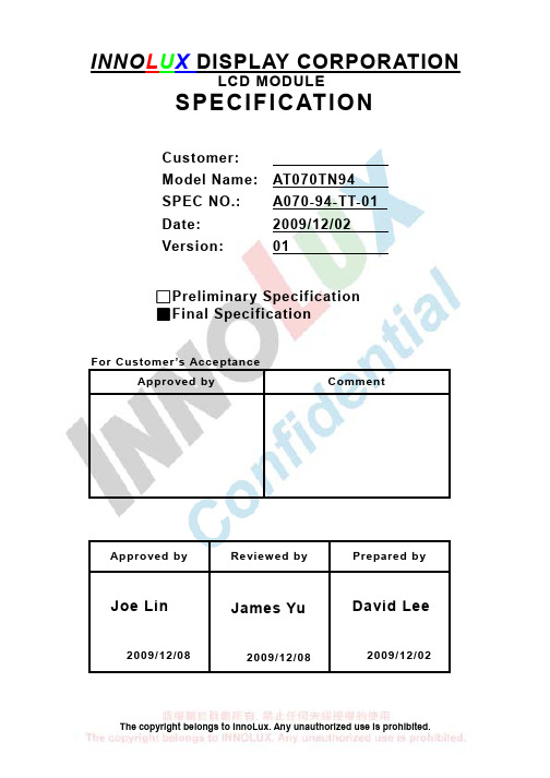
The copyright belongs to InnoLux. Any unauthorized use is prohibited.INNO L U X DISPLAY CORPORATIONLCD MODULESPECIFICATIONCustomer: Model Name: AT070TN94SPEC NO.: A070-94-TT-01 Date: 2009/12/02 Version:01□Preliminary Specification ■Final SpecificationFor Customer ’s AcceptanceApproved byCommentApproved byReviewed by Prepared byJoe Lin2009/12/08James Yu2009/12/08David Lee2009/12/02InnoLux copyright 2004All rights reserved,Copying forbidden.Record of RevisionVersion Revise Date Page ContentPre-Spec.01 2009/07/07 All Initial ReleaseFinal-spec.01 2009/12/02 All The first version final specification.6 Modify V COM to 3.8V(Typ.), 3.6V(Min.) and 4.0V(Max.).9 Add Input Clock and Data Timing Diagram.18 Update the Mechanical Drawing.The copyright belongs to InnoLux. Any unauthorized use is prohibited.I NNO L U XContents1. General Specifications (1)2. Pin Assignment (2)3. Operation Specifications (5)3.1. Absolute Maximum Ratings (5)3.1.1. Typical Operation Conditions (6)3.1.2. Current Consumption (7)3.1.3. Backlight Driving Conditions (7)3.2. Power Sequence (8)3.3. Timing Characteristics (9)3.3.1. AC Electrical Characteristics (9)3.3.2. Input Clock and Data Timing Diagram (9)3.3.3. Timing (10)3.3.4. Data Input Format (11)4. Optical Specifications (12)5. Reliability Test Items (16)6. General Precautions (17)6.1. Safety (17)6.2. Handling (17)6.3. Static Electricity (17)6.4. Storage (17)6.5. Cleaning (17)7. Mechanical Drawing (18)8. Package Drawing (19)8.1. Packaging Material Table (19)8.2. Packaging Quantity (19)8.3. Packaging Drawing (20)The copyright belongs to InnoLux. Any unauthorized use is prohibited.1. General SpecificationsNo. Item Specification Remark1 LCD size 7.0 inch(Diagonal)2 Driver element a-Si TFT active matrix3 Resolution 800 × 3(RGB) × 4804 Display mode Normally White, Transmissive5 Dot pitch 0.0642(W) × 0.1790(H) mm6 Active area 154.08(W) × 85.92(H) mm7 Module size 164.9(W) ×100.0(H) ×5.7(D) mm Note 18 Surface treatment Anti-Glare9 Color arrangement RGB-stripe10 Interface Digital11 Backlight power consumption 1.674W (Typ.)12 Panel power consumption 0.226W (Typ.)13 Weight 150g (Typ.)Note 1: Refer to Mechanical Drawing.2. Pin AssignmentFPC Connector is used for the module electronics interface. The recommended model is FH12A-50S-0.5SH manufactured by Hirose.Pin No. Symbol I/O Function Remark1 V LED+P Power for LED backlight (Anode)2 V LED+P Power for LED backlight (Anode)3 V LED-P Power for LED backlight (Cathode)4 V LED-P Power for LED backlight (Cathode)5 GND P Power ground6 V COM I Common voltage7 DV DD P Power for Digital Circuit8 MODE I DE/SYNC mode select Note 19 DE I Data Input Enable10 VS I Vertical Sync Input11 HS I Horizontal Sync Input12 B7 I Blue data(MSB)13 B6 I Blue data14 B5 I Blue data15 B4 I Blue data16 B3 I Blue data17 B2 I Blue data18 B1 I Blue data Note 219 B0 I Blue data(LSB) Note 220 G7 I Green data(MSB)21 G6 I Green data22 G5 I Green data23 G4 I Green data24 G3 I Green data25 G2 I Green data26 G1 I Green data Note 227 G0 I Green data(LSB) Note 228 R7 I Red data(MSB)29 R6 I Red data30 R5 I Red data31 R4 I Red data32 R3 I Red data33 R2 I Red data34 R1 I Red data Note 235 R0 I Red data(LSB) Note 236 GND P Power Ground37 DCLK I Sample clock Note 338 GND P Power Ground39 L/R I Left / right selection Note 4,540 U/D I Up/down selection Note 4,541 V GH P Gate ON Voltage42 V GL P Gate OFF Voltage43 AV DD P Power for Analog Circuit44 RESET I Global reset pin. Note 645 NC - No connection46 V COM I Common Voltage47 DITHB I Dithering function Note 748 GND P Power Ground49 NC - No connection50 NC - No connectionI: input, O: output, P: PowerNote 1: DE/SYNC mode select. Normally pull high.When select DE mode, MODE=”1”, VS and HS must pull high.When select SYNC mode,MODE= ”0”, DE must be grounded.Note 2: When input 18 bits RGB data, the two low bits of R,G and B data must be grounded.Note 3:Data shall be latched at the falling edge of DCLK.Note 4: Selection of scanning modeSetting of scan control inputU/D L/R Scanning direction GND DV DD Up to down, left to right DV DD GND Down to up, right to left GND GND Up to down, right to left DV DDDV DDDown to up, left to rightNote 5: Definition of scanning direction. Refer to the figure as below:Note 6: Global reset pin. Active low to enter reset state. Suggest to connect with an RCreset circuit for stability. Normally pull high.Note 7: Dithering function enable control, normally pull high. When DITHB=”1”,Disable internal dithering function, When DITHB=”0”,Enable internal dithering function,RightLeft DownUp3. Operation Specifications3.1. Absolute Maximum Ratings(Note 1)ValuesItem SymbolMin. Max.Unit RemarkDV DD -0.3 5.0 VAV DD 6.5 13.5 VV GH -0.3 40.0 VV GL -20.0 0.3 V Power voltageV GH-V GL- 40.0 V Operation Temperature T OP -30 85 ℃Storage Temperature T ST-30 85 ℃LED Reverse Voltage V R- 1.2 VEach LEDNote 2 LED Forward Current I F- 25 mA Each LEDNote 1: The absolute maximum rating values of this product are not allowed to be exceeded at any times. Should a module be used with any of the absolute maximum ratingsexceeded, the characteristics of the module may not be recovered, or in an extremecase, the module may be permanently destroyed.Note 2: V R Conditions: Zener Diode 20mA3.1.1. Typical Operation Conditions( Note 1)ValuesUnit Remark Item SymbolMin. Typ. Max.DV DD 3.0 3.3 3.6 V Note 2AV DD 10.2 10.4 10.6 VPower voltageV GH 15.3 16.0 16.7 VV GL -7.7 -7.0 -6.3 VInput signal voltage V COM 3.6 3.8 4.0 VInput logic high voltage V IH 0.7 DV DD - DV DD VNote 3 Input logic low voltage V IL 0 - 0.3 DV DD VNote 1: Be sure to apply DV DD and V GL to the LCD first, and then apply V GH.Note 2: DV DD setting should match the signals output voltage (refer to Note 3) of customer’s system board.Note 3: DCLK,HS,VS,RESET,U/D, L/R,DE,R0~R7,G0~G7,B0~B7,MODE,DITHB.3.1.2. Current ConsumptionValuesItem SymbolMin. Typ. Max.Unit RemarkI GH - 0.2 1.0 mA V GH =16.0VI GL - 0.2 1.0 mA V GL = -7.0V IDV DD - 4.0 10 mA DV DD =3.3VCurrent for DriverIAV DD - 20 50 mA AV DD =10.4V3.1.3. Backlight Driving ConditionsValuesItem SymbolMin. Typ. Max.Unit Remark Voltage for LED backlight V L 8.4 9.3 10.2 V Note 1 Current for LED backlight I L 170 180 200 mALED life time - 20,000 - - Hr Note 2Note 1: The LED Supply Voltage is defined by the number of LED at Ta=25℃ andI L =180mA.Note 2: The “LED life time” is defined as the module brightness decrease to 50% original brightness at Ta=25℃ and I L =180mA. The LED lifetime could be decreased ifoperating I L is lager than 180mA.3.2. Power Sequencea. Power on:Note: Data include R0~R7, B0~B7, GO~G7, U/D, L/R, DCLK, HS,VS,DE.DV DD→VGL→AVDD→VGH→Data→B/LB/L→Data→VGH→AVDD→VGL→DV DD3.3. Timing Characteristics3.3.1. AC Electrical CharacteristicsValuesItem SymbolMin. Typ. Max.Unit Remark HS setup time T hst8 - - nsHS hold time T hhd 8 - - nsVS setup time T vst8 - - nsVS hold time T vhd8 - - nsData setup time T dsu8 - - nsData hole time T dhd8 - - nsDE setup time T esu 8 - - nsDE hole time T ehd8 - - nsDV DD Power On Slew rate T POR - - 20 ms From 0 to 90% DV DDRESET pulse width T Rst 1 - - ms DCLK cycle time T coh 20 - - ns DCLK pulse duty T cwh 40 50 60 %3.3.2. Input Clock and Data Timing Diagram3.3.3. TimingValuesUnit Remark Item SymbolMin. Typ. Max.Horizontal Display Area thd- 800 - DCLKDCLK Frequency fclk26.4 33.3 46.8 MHzOne Horizontal Line th862 1056 1200 DCLKHS pulse width thpw 1 - 40 DCLKHS Blanking thb46 46 46 DCLKHS Front Porch thfp 16 210 354 DCLKValuesItem SymbolUnit RemarkMin. Typ. Max.Vertical Display Area tvd- 480 - THVS period time tv 510 525 650 THVS pulse width tvpw 1 - 20 THVS Blanking tvb23 23 23 THVS Front Porch tvfp7 22 147 TH3.3.4. Data Input Format4. Optical SpecificationsValuesItem Symbol ConditionMin. Typ. Max.Unit RemarkθL Φ=180°(9 o’clock) 60 70 -θRΦ=0°(3 o’clock) 60 70 -θTΦ=90°(12 o’clock) 40 50 -Viewing angle(CR≥ 10)θBΦ=270°(6 o’clock) 60 70 -degree Note 1T ON - 10 20 msec Note 3 Response timeT OFF - 15 30 msec Note 3 Contrast ratio CR 400 500 - - Note 4W X 0.26 0.31 0.36 -Color chromaticityW Y 0.28 0.33 0.38 -Note 2Note 5Note 6 Luminance L 320 400 - cd/m² Note 6 LuminanceuniformityY UNormalθ=Φ=0°70 75 - % Note 7Test Conditions:1. DV DD=3.3V, I L=180mA (Backlight current), the ambient temperature is 25℃.2. The test systems refer to Note 2.Note 1: Definition of viewing angle rangeFig. 4-1 Definition of viewing angleNote 2: Definition of optical measurement system.The optical characteristics should be measured in dark room. After 30 minutesoperation, the optical properties are measured at the center point of the LCD screen. (Response time is measured by Photo detector TOPCON BM-7, other items are measured by BM-5A/Field of view: 1° /Height: 500mm.)Normal line θ=Φ=0°Photo detectorΦ=90°12 o’clock directionΦ=270° 6 o’clock directionΦ=0°Φ=180°Active Area500mmLCMNormal line θ=Φ=0°Φ=90°12 o’clock directionΦ=270°6 o’clock directionΦ=0°Φ=180°Active AreaθLθTθBθRLCMNote 3: Definition of Response timeThe response time is defined as the LCD optical switching time interval between“White” state and “Black” state. Rise time (T ON) is the time between photo detector output intensity changed from 90% to 10%. And fall time (T OFF) is the timebetween photo detector output intensity changed from 10% to 90%.Fig. 4-3 Definition of response timeNote 4: Definition of contrast ratiostateBlack""theonLCDwhenmeasuredLuminancestateWhite""theonLCDwhenmeasuredLuminance(CR)ratioContrast=Note 5: Definition of color chromaticity (CIE1931)Color coordinates measured at center point of LCD.Note 6: All input terminals LCD panel must be ground while measuring the center area of the panel.The LED driving condition is I L=180mA .90%10%0%Photodetectoroutput(Relativevalue)ONTWhite (TFT OFF) Black (TFT ON) White (TFT OFF)Note 7:Definition of Luminance UniformityActive area is divided into 9 measuring areas (Refer to Fig. 4-4 ).Every measuring point is placed at the center of each measuring area.maxminBB(Yu)UniformityLuminance=L-------Active area length W----- Active area widthWW/3W/3W/6L/3L/3L/6LFig. 4-4 Definition of measuring pointsB max: The measured maximum luminance of all measurement position.B min: The measured minimum luminance of all measurement position.5. Reliability Test Items(Note3)Item Test Conditions Remark High Temperature Storage Ta = 85℃240hrs Note 1,Note 4 Low Temperature Storage Ta = -30℃240hrs Note 1,Note 4 High Temperature Operation Ts = 85℃240hrs Note 2,Note 4 Low Temperature Operation Ta = -30℃240hrs Note 1,Note 4 Operate at High Temperatureand Humidity+60℃, 90%RH 240hrs Note 4Thermal Shock -30℃/30 min ~ +85℃/30 min for a total 100cycles, Start with cold temperature and endwith high temperature.Note 4Vibration Test Frequency range:10~55Hz Stroke:1.5mmSweep:10Hz~55Hz~10Hz2 hours for each direction of X. Y. Z.(6 hours for total)Mechanical Shock 100G 6ms,±X, ±Y, ±Z 3 times for each directionPackage Vibration Test Random Vibration :0.015G*G/Hz from 5-200HZ, -6dB/Octave from 200-500HZ2 hours for each direction of X. Y. Z.(6 hours for total)Package Drop Test Height:60 cm1 corner, 3 edges, 6 surfacesElectro Static Discharge ± 2KV, Human Body Mode, 100pF/1500ΩNote 1: Ta is the ambient temperature of samples.Note 2: Ts is the temperature of panel’s surface.Note 3: In the standard condition, there shall be no practical problem that may affect the display function. After the reliability test, the product only guarantees operation,but don’t guarantee all of the cosmetic specification.Note 4: Before cosmetic and function test, the product must have enough recovery time, at least 2 hours at room temperature.6. General Precautions6.1. SafetyLiquid crystal is poisonous. Do not put it in your mouth. If liquid crystal touches your skin or clothes, wash it off immediately by using soap and water.6.2. Handling1. The LCD panel is plate glass. Do not subject the panel to mechanical shock or toexcessive force on its surface.2. The polarizer attached to the display is easily damaged. Please handle it carefullyto avoid scratch or other damages.3. To avoid contamination on the display surface, do not touch the module surfacewith bare hands.4. Keep a space so that the LCD panels do not touch other components.5. Put cover board such as acrylic board on the surface of LCD panel to protect panelfrom damages.6. Transparent electrodes may be disconnected if you use the LCD panel underenvironmental conditions where the condensation of dew occurs.7. Do not leave module in direct sunlight to avoid malfunction of the ICs.6.3. Static Electricity1. Be sure to ground module before turning on power or operating module.2. Do not apply voltage which exceeds the absolute maximum rating value.6.4. Storage1. Store the module in a dark room where must keep at 25±10℃ and 65%RH or less.2. Do not store the module in surroundings containing organic solvent or corrosivegas.3. Store the module in an anti-electrostatic container or bag.6.5. Cleaning1. Do not wipe the polarizer with dry cloth. It might cause scratch.2. Only use a soft sloth with IPA to wipe the polarizer, other chemicals mightpermanent damage to the polarizer.7. Mechanical Drawing8. Package Drawing8.1. Packaging Material TableNo. ItemModel(Material)Dimensions(mm)UnitWeight(kg)Quantity Remark1 LCMModuleAT070TN94 164.9 × 100.0 × 5.7 0.150 50pcs2 Partition BC Corrugatedpaper512 × 349 × 226 1.466 1set3 CorrugatedPaperB Corrugatedpaper510 × 350 0.071 4pcs4 CorrugatedBarB Corrugatedpaper512 × 11 × 3 0.046 4pcs5 Dust-ProofBagPE 700 × 530 0.048 1pcs6 A/S Bag PE 180 × 133 × 0.2 0.002 50pcs7 Carton Corrugatedpaper530 × 355 × 255 1.100 1pcs8 Total weight 10.682 kg± 5%8.2. Packaging QuantityTotal LCM quantity in Carton: no. of Partition 2 Rows × quantity per Row 25 = 508.3. Packaging Drawing。
电阻式触摸屏规格书(中小尺寸)

3H pencil, pressure 1N/45°
[鉛筆 3H,壓力 1N/45°(JIS K5400)]
≧3H
800g by vertical 90°
Satisfy (1) of Item 6
[800g , 垂直 90°]
135°10 times left & right
[符合 6 項目(1)]
[此規格適用於五線-類比電阻式觸控屏幕]
Item [項目] (1) Type
[型式]
(2) Input Mode [操作模式]
(3) Cable [連結線]
Specifications [規格] Five-Wire Analog Resistive
[五線-類比電阻式]
Stylus or Finger
Satisfy (1) of Item 6
[135°角,左右來回 10 次]
[符合 6 項目(1)]
08. Reliability
[可靠度]
Item [項目] High Temperature /Humidity
[高溫高濕]
High temperature
[高溫]
Low temperature
[低溫]
萬達光電科技股份有限公司
PRODUCT SPECIFICATIONS 產品規範書
Customer (客戶): Model (型式): T121S-5RA006N-0A18R0-200FH Mode (種類): Five-wire Analog Touch Panel Date (日期): Sep. 16, 2008
Hardness
[硬度]
Peeling
[剝離]
32-37超薄LED电源
• 当电源的输出端电压12V或24V电压增大时,由于 REF>2.5V,则AS431内部比较器的输出高电平从而使 NPN管导通。IC605即光电耦合器的2脚位电位随着降 低,显然这种变化势必会使得流过光电耦合器的发光 二极管的电流有所增大。由于光电耦合器817C的CTR (电流传感系数即流过发光二极管的电流与流过光敏 三极管的电流的比值)约等于1,使得从817C中的光 敏三极管的2脚(FB)流过的电流也有所增大,这导致 5641 PIN2 (FB)端电压降低,控制IC输出脉冲占空比 变小,使次级输出电压降低,所以达到降压的目的。 输出电压下降;同理,当输出电压降低时,AS431内 部比较器的输出低电平从而使NPN截止,从而使得流 过光电耦合器的发光二极管的电流减小,可使5641 PIN2 (FB)端电压升高,于是IC输出脉冲占空比变大, 输出电压上升。
• 4)各控制电路输出整流稳压电路。
输出整流电路由二极管组成的半波整流电路。
电源方框图
三、各电路分述
• 1、EMI防护与滤波电路
¤交流输入与EMI滤波电路。基本工作过程为,市电经由V601、CX6001、 L600、CY601、CY602、CX6002、L601、BD1等组成的整流滤波电路后 转变成脉动直流. ¤CX6001、L600、CY601、CY602、CX6002、L601等组成的整流滤波 电路主要是防止外界的杂讯信号对电源的干扰以及电源的开关杂讯对电网 产生的干扰。此部分电路的作用就是我们熟称为的EMI抑制电路。
1).待机电路
• ①原理及内部框图:此待机芯片为Sanken公司的 STR-A6059M,它是一个集成块,里面集成了控制 芯片与开关管。外形如下图所示:
• 此芯片最大功率可做到14W左右。
N133HSE-EA3 屏规格书

Doc. Number:□ Tentative Specification ■ Preliminary Specification □ Approval SpecificationMODEL NO: N133HSESUFFIX: EA3Approved ByChecked ByPrepared ByCONTENTS1. GENERAL DESCRIPTION (5)1.1 OVERVIEW (5)1.2 GENERAL SPECIFICATI0NS (5)2. MECHANICAL SPECIFICATIONS (5)2.1 CONNECTOR TYPE (5)3. ABSOLUTE MAXIMUM RATINGS (6)3.1 ABSOLUTE RATINGS OF ENVIRONMENT (6)3.2 ELECTRICAL ABSOLUTE RATINGS (6)3.2.1 TFT LCD MODULE (6)4. ELECTRICAL SPECIFICATIONS (7)4.1 FUNCTION BLOCK DIAGRAM (7)4.2. INTERFACE CONNECTIONS (7)4.3 ELECTRICAL CHARACTERISTICS (9)4.3.1 LCD ELETRONICS SPECIFICATION (9)4.3.2 LED CONVERTER SPECIFICATION (11)4.3.3 BACKLIGHT UNIT (13)4.4 DISPLAY PORT SIGNAL TIMING SPECIFICATION (14)4.4.1 DISPLAY PORT INTERFACE (14)4.5 DISPLAY TIMING SPECIFICATIONS (15)4.6 POWER ON/OFF SEQUENCE (16)5. OPTICAL CHARACTERISTICS (19)5.1 TEST CONDITIONS (19)5.2 OPTICAL SPECIFICATIONS (19)6. RELIABILITY TEST ITEM (22)7. PACKING (23)7.1 MODULE LABEL (23)7.2 CARTON (24)7.3 PALLET (25)7.4 UN-PACK METHOD (26)8. PRECAUTIONS (27)8.1 HANDLING PRECAUTIONS (27)8.2 STORAGE PRECAUTIONS (27)8.3 OPERATION PRECAUTIONS (27)Appendix. EDID DATA STRUCTURE (28)Appendix. OUTLINE DRAWING (31)Appendix. SYSTEM COVER DESIGN GUIDANCE (33)Appendix. LCD MODULE HANDLING MANUAL (40)REVISION HISTORYVersion Date Page Description0.0 Jan,22,2014 All Tentative spec. ver. 0.0 was first issued.1.0 Apr,8,2014 All Preliminary spec. ver. 1.0 was first issued.1. GENERAL DESCRIPTION 1.1 OVERVIEWN133HSE-EA3 is a 13.3” (13.3” diagonal) TFT Liquid Crystal Display module with LED Backlight unit and 30 pins EDP interface. This module supports 1920 x 1080 FHD model and can display 16,777,216 colors. The optimum viewing angle is at 6 o’clock direction.1.2 GENERAL SPECIFICATI0NSItemSpecification Unit Note Screen Size 13.3 diagonal Driver Element a-si TFT active matrix - - Pixel Number 1920 x R.G.B. x 1080 pixel - Pixel Pitch0.1529 (H) x 0.1529 (V) mm - Pixel Arrangement RGB vertical stripe - - Display Colors16,777,216 color - Transmissive Mode Normally black - - Surface Treatment Hard coating (3H), Anti-Glare - - Luminance, White 350 Cd/m2 Power ConsumptionTotal (5.77) W(Max.) @ cell (0.86)W(Max.), BL (4.91) W(Max.)(1)Note (1) The specified power consumption (with converter efficiency) is under the conditions at VCCS = 3.3 V, fv = 60 Hz, LED_VCCS = Typ, fPWM = 200 Hz, Duty=100% and Ta = 25 ± 2 ºC, whereas mosaic2. MECHANICAL SPECIFICATIONSItem Min. Typ. Max. Unit Note Horizontal (H)304.85 305.35 305.85 mm Vertical (V) (W/ PCBA)(193.27) (193.77) (194.27) mm Module Size Thickness (T) NA (2.85) (3.00) mm (1) Horizontal293.66 293.76 293.86 mm Active AreaVertical165.14 165.24 165.34 mm Weight-(245)(260)gNote (1) Please refer to the attached drawings for more information of front and back outline dimensions.2.1 CONNECTOR TYPEPlease refer Appendix Outline Drawing for detail design.Connector Part No.: IPEX-20455-030E-12 User’s connector Part No: IPEX-20453-030T-01Pin1Pin303. ABSOLUTE MAXIMUM RATINGS3.1 ABSOLUTE RATINGS OF ENVIRONMENTValueItemSymbol Min. Max. Unit Note Storage TemperatureT ST -20 +60 ºC (1) Operating Ambient Temperature T OP+50ºC(1), (2)Note (1) (a) 90 %RH Max. (Ta < 40 ºC).(b) Wet-bulb temperature should be 39 ºC Max. (Ta < 40 ºC).(c) No condensation.Note (2) The temperature of panel surface should be 0 ºC min. and 50 ºC max.3.2 ELECTRICAL ABSOLUTE RATINGS 3.2.1 TFT LCD MODULEValue ItemSymbol Min. Max. Unit Note Power Supply Voltage VCCS (-0.3) (+4.0) V Logic Input Voltage V IN (-0.3) (VCCS+0.3)V(1) Converter Input VoltageLED_VCCS (-0.3) (25) V (1) Converter Control Signal Voltage LED_PWM, (-0.3) (5) V (1) Converter Control Signal VoltageLED_EN(-0.3)(5)V(1)Note (1) Stresses beyond those listed in above “ELECTRICAL ABSOLUTE RATINGS” may causepermanent damage to the device. Normal operation should be restricted to the conditions described in “ELECTRICAL CHARACTERISTICS”.4. ELECTRICAL SPECIFICATIONS 4.1 FUNCTION BLOCK DIAGRAM4.2. INTERFACE CONNECTIONSPIN ASSIGNMENT Pin Symbol DescriptionRemark1 NC No Connection (Reserved for INX test)2 H_GND High Speed Ground3 ML1- Complement Signal-Lane 14 ML1+ True Signal-Main Lane 15 H_GND High Speed Ground6 ML0- Complement Signal-Lane 07 ML0+ True Signal-Main Lane 08 H_GND High Speed Ground9 AUX+ True Signal-Auxiliary Channel10 AUX- Complement Signal-Auxiliary Channel 11 H_GND High Speed Ground12 VCCS Power Supply +3.3 V (typical) 13 VCCS Power Supply +3.3 V (typical)14 NC No Connection (Reserved for INX test) 15 GND Ground 16 GND Ground17 HPD Hot Plug Detect 18 BL_GND BL Ground 19 BL_GND BL Ground 20 BL_GND BL Ground 21 BL_GND BL Ground22LED_ENBL_Enable Signal of LED ConverterSignalsGNDConverter Input Signals23 LED_PWM PWM Dimming Control Signal of LED Converter24 NC No Connection (Reserved for INX test) 25 NC No Connection (Reserved for INX test) 26 LED_VCCS BL Power27 LED_VCCS BL Power 28 LED_VCCS BL Power 29 LED_VCCSBL Power30NCNo Connection (Reserved for INX test)Note (1) The first pixel is odd as shown in the following figure.4.3 ELECTRICAL CHARACTERISTICS4.3.1 LCD ELETRONICS SPECIFICATIONValueParameter SymbolMin. Typ. Max.UnitNotePower Supply Voltage VCCS (3.0) (3.3) (3.6) V(1)-High Level (3.0) - (3.6) VHPDLow Level (0) - (0.4) VRipple Voltage V RP- (50) - mV (1)- Inrush Current I RUSH- - (1.5) A (1),(2)Mosaic - (244) (262) mA(3)aPower Supply CurrentWhite lcc- (271) (310) mA (3)bNote (1) The ambient temperature is Ta = 25 ± 2 ºC.Note (2) I RUSH: the maximum current when VCCS is risingI IS: the maximum current of the first 100ms after power-onMeasurement Conditions: Shown as the following figure. Test pattern: white.SWVCCS +3.3VVCCS rising time is 0.5msNote (3) The specified power supply current is under the conditions at VCCS = 3.3 V, Ta = 25 ± 2 ºC, DCCurrent and f v = 60 Hz, whereas a power dissipation check pattern below is displayed.Active Areaa. Mosaic PatternActive Areab. White Pattern4.3.2 LED CONVERTER SPECIFICATIONValueParameterSymbolMin.Typ. Max. UnitNote Converter Input power supply voltage LED_Vccs (5.0) (12.0) (21.0) V Converter Inrush CurrentILED RUSH- - (1.5) A (1) Backlight On(2.2)-(5.0)VEN Control LevelBacklight Off(0) - (0.6) V PWM High Level(2.2)-(5.0)VPWM Control LevelPWM Low Level(0) - (0.6) V PWM Control Duty Ratio(5) - (100) % PWM Control PermissiveRipple VoltageV PWM_pp- - (100) mV PWM Control Frequencyf PWM (190) - (1K) Hz (2) LED Power Current LED_VCCS =Typ.ILED (302)(357)(409)mA(3)Note (1) ILED RUSH : the maximum current when LED_VCCS is rising, ILED IS : the maximum current of the first 100ms after power-on,Measurement Conditions: Shown as the following figure. LED_VCCS = Typ, Ta = 25 ± 2 ºC, f PWM = 200 Hz, Duty=100%.LED_VCCS(Typ)ILEDLED_VCCLED_PWM LED_ENNote (2)If PWM control frequency is applied in the range less than 1KHz, the “waterfall” phenomenon onthe screen may be found. To avoid the issue, it’s a suggestion that PWM control frequency should follow the criterion as below.PWM control frequency f PWM should be in the range≤∗+f N )33.0( f PWM f N ∗+≤)66.0(N : Integer )3(≥Nf : Frame rateNote (3) The specified LED power supply current is under the conditions at “LED_VCCS = Typ.”, Ta = 25± 2 ºC, f PWM = 200 Hz, Duty=100%.VLED rising time is 0.5ms4.3.3 BACKLIGHT UNITTa = 25 ± 2 ºCValue ParameterSymbol Min. Typ. Max. Unit NoteLED Light Bar Power Supply VoltageV L 23.426.1 28.8VLED Light Bar Power Supply CurrentI L 126mA(1)(2)(Duty100%)Power Consumption P L - 3.2886 3.6288 W (3) LED Life Time L BL15000 --Hrs(4)Note (1) LED current is measured by utilizing a high frequency current meter as shown below :Note (2) For better LED light bar driving quality, it is recommended to utilize the adaptive boost converter withcurrent balancing function to drive LED light-bar.Note (3) P L = I L ×V L (Without LED converter transfer efficiency)Note (4) The lifetime of LED is defined as the time when it continues to operate under the conditions at Ta = 25 ±2oC and I L = 21 mA (Per EA) until the brightness becomes 50% of its original value.≦V I Channels4.4 DISPLAY PORT SIGNAL TIMING SPECIFICATION 4.4.1 DISPLAY PORT INTERFACEParameterSymbol Min. Typ. Max. Unit Notes Differential Signal Common Mode Voltage(MainLink and AUX) VCM (0) (2) V (1)(3) AUX AC Coupling CapacitorC AUX(75)(200)nF(2)Note (1) Display port interface related AC coupled signals should follow VESA DisplayPort StandardVersion1. Revision 1a and VESA Embedded DisplayPort TMStandard Version 1.1.(2) The AUX AC Coupling Capacitor should be placed on Source Devices.(3)The source device should pass the test criteria described in DisplayPortCompliance TestSpecification (CTS) 1.10VV CM |Single EndedV D+ V D-4.5 DISPLAY TIMING SPECIFICATIONSThe input signal timing specifications are shown as the following table and timing diagram . Refresh rate 60Hz Signal Item Symbol Min.Typ.Max.UnitNote DCLKFrequency 1/Tc (116.17) (138.78) (142.77) MHz - Vertical Total Time TV (1103) (1112) (1462) TH - Vertical Active Display PeriodTVD (1080) (1080) (1080) TH - Vertical Active Blanking PeriodTVB TV-TVD (32) TV-TVDTH - Horizontal Total Time TH (2058) (2080) (2910) Tc- Horizontal Active Display Period THD (1920)(1920) (1920)Tc - DEHorizontal Active Blanking PeriodTHBTH-THD(160)TH-THDTc-INPUT SIGNAL TIMING DIAGRAMDCLKDEDEDATA4.6 POWER ON/OFF SEQUENCERestartPower OnPower Off-Power Supplyfor LCD, VCCS -eDP Display-HPD from Sink -AUX Channel -Main Link Data- LED Converter,LED_VCCS - LED Converter LED_PWM - LED Converter Enable Signal, LED_ENTiming Specifications: Value ParameterDescriptionReqd. By Min Max Unit Notes t1Power rail rise time, 10% to 90% Source0.5 10ms-t2 Delay from LCD,VCCS to black video generationSink 0 200 msAutomatic Black Videogeneration prevents display noise until valid video data is received from the Source (see Notes:2 and 3 below) t3Delay from LCD,VCCS to HPD highSink 0 200 ms Sink AUX Channel must be operational upon HPD high (see Note:4 below )t4 Delay from HPD high to link training initialization Source - - ms Allows for Source to read Link capability and initializet5Link training durationSource--ms Dependant on Source link training protocol t6 Link idle Source - -msMin Accounts for required BS-Idlepattern. Max allows for Source frame synchronizationt7Delay from valid video data from Source to video on displaySink 0 50msMax value allows for Sink to validate video data and timing. At the end of T7, Sink willindicate the detection of valid video data by setting theSINK_STATUS bit to logic 1 (DPCD 00205h, bit 0), and Sink will no longer generateautomatic Black Video t8Delay from valid video data from Source to backlight onSource - -msSource must assure display video is stable t9Delay from backlight off to end of valid video dataSource - -msSource must assure backlight is no longer illuminated. At the end of T9, Sink will indicate the detection of no valid video data by setting the SINK_STATUS bit to logic 0 (DPCD00205h, bit 0), and Sink will automatically display Black Video. (See Notes: 2 and 3 below)t10 Delay from end of valid video data from Source to power off Source 0 500 ms Black video will be displayed after receiving idle or off signals from Sourcet11 VCCS power rail fall time, 90% to 10%Source 0.5 10 ms - t12 VCCS Power off timeSource 500 - ms - t A LED power rail rise time, 10% to 90%Source 0.5 10 ms - t BLED power rail fall time, 90% to 10%Source10ms-t C Delay from LED power rising to LED dimming signalSource 1 - ms - t D Delay from LED dimming signal to LED power fallingSource 1 - ms - t E Delay from LED dimming signal to LED enable signalSource 1 - ms - t FDelay from LED enable signal to LED dimming signalSource1-ms-Note (1) Please don’t plug or unplug the interface cable when system is turned on.Note (2) The Sink must include the ability to automatically generate Black Video autonomously. The Sink mustautomatically enable Black Video under the following conditions:- Upon LCDVCC power-on (within T2 max)- When the “NoVideoStream_Flag” (VB-ID Bit 3) is received from the Source (at the end of T9) Note (3) The Sink may implement the ability to disable the automatic Black Video function, as described inNote (2), above, for system development and debugging purposes.Note (4) The Sink must support AUX Channel polling by the Source immediately following LCDVCCpower-on without causing damage to the Sink device (the Source can re-try if the Sink is not ready). The Sink must be able to response to an AUX Channel transaction with the time specified within T3 max.5. OPTICAL CHARACTERISTICS5.1 TEST CONDITIONSItem Symbol Value Unit Ambient Temperature Ta 25±2 o CAmbient Humidity Ha 50±10 %RHSupply Voltage V CC 3.3 VInput Signal According to typical value in "3. ELECTRICAL CHARACTERISTICS"LED Light Bar Input Current I L(126) mAThe measurement methods of optical characteristics are shown in Section 5.2. The following items should be measured under the test conditions described in Section 5.1 and stable environment shown in Note (5).Note (2) Definition of Contrast Ratio (CR):The contrast ratio can be calculated by the following expression. Contrast Ratio (CR) = L63 / L0 L63: Luminance of gray level 63 L 0: Luminance of gray level 0 CR = CR (1)CR (X) is corresponding to the Contrast Ratio of the point X at Figure in Note (6).Note (3) Definition of Response Time (T R , T F ):Note (4) Definition of Average Luminance of White (L AVE ):Measure the luminance of gray level 63 at 5 pointsL AVE = [L (1)+ L (2)+ L (3)+ L (4)+ L (5)] / 5L (x) is corresponding to the luminance of the point X at Figure in Note (6)100% 90%10% 0%OpticalNote (5) Measurement Setup:The LCD module should be stabilized at given temperature for 20 minutes to avoid abrupt temperature change during measuring. In order to stabilize the luminance, the measurement should be executed after lighting Backlight for 20 minutes in a windless room.Note (6) Definition of White Variation (δW):Measure the luminance of gray level 63 at 5 points δW 5p = {Minimum [L (1)~L (5)] / Maximum [L (1)~ L (5)]}*100%Note (7) The listed optical specifications refer to the initial value of manufacture, but the condition ofthe specifications after long-term operation will not be warranted.: Test Point X=1 to 136. RELIABILITY TEST ITEMTest Item Test Condition Note High Temperature Storage Test 60ºC, 240 hoursLow Temperature Storage Test -20ºC, 240 hoursThermal Shock Storage Test -20ºC, 0.5hour←→60, 0.5hour; 100cycles, 1hour/cycle℃High Temperature Operation Test 50ºC, 240 hoursLow Temperature Operation Test 0ºC, 240 hoursHigh Temperature & High HumidityOperation Test50ºC, RH 80%, 240hoursHigh Temperature & High Humidity Storage Test 40ºC, RH 90%, 240hours(1) (2)ESD Test (Operation) 150pF, 330Ω, 1sec/cycleCondition 1 : Contact Discharge, ±8KVCondition 2 : Air Discharge, ±15KV(1)Shock (Non-Operating) 220G, 2ms, half sine wave,1 time for each direction of±X,±Y,±Z(1)(3)Vibration (Non-Operating) 1.5G / 10-500 Hz, Sine wave, 30 min/cycle, 1cycle for eachX, Y, Z(1)(3)Note (1) criteria : Normal display image with no obvious non-uniformity and no line defect.Note (2) Evaluation should be tested after storage at room temperature for more than two hourNote (3) At testing Vibration and Shock, the fixture in holding the module has to be hard and rigid enough so that the module would not be twisted or bent by the fixture.7. PACKING7.1 MODULE LABELThe barcode nameplate is pasted on each module as illustration, and its definitions are as following explanation.(a) Model Name: N133HSE – EA3(b) Revision: Rev. XX, for example: C1, C2 …etc. (c)(d) Production Location: MADE IN XXXX. (e) UL Logo: XXXX is UL factory ID.Serial ID includes the information as below:(a) Manufactured Date: Year: 0~9, for 2010~2019Month: 1~9, A~C, for Jan. ~ Dec.Day: 1~9, A~Y , for 1stto 31st, exclude I , O and U(b) Revision Code: cover all the change(c) Serial No.: Manufacturing sequence of product (d) Product Line: 1 -> Line1, 2 -> Line 2, …etc.Product Line Year, Month, Date INX Internal Use RevisionINX Internal UseSerial No. CT:CDSQRRR5CWWXXXN133HSE-EA3 Rev. XX7.2 CARTONFigure. 7-1 Packing method7.3 PALLET7.4 UN-PACK METHODFigure. 7-3 Un-Packing method8. PRECAUTIONS8.1 HANDLING PRECAUTIONS(1) The module should be assembled into the system firmly by using every mounting hole. Be carefulnot to twist or bend the module.(2) While assembling or installing modules, it can only be in the clean area. The dust and oil may causeelectrical short or damage the polarizer.(3) Use fingerstalls or soft gloves in order to keep display clean during the incoming inspection andassembly process.(4) Do not press or scratch the surface harder than a HB pencil lead on the panel because the polarizeris very soft and easily scratched.(5) If the surface of the polarizer is dirty, please clean it by some absorbent cotton or soft cloth. Do notuse Ketone type materials (ex. Acetone), Ethyl alcohol, Toluene, Ethyl acid or Methyl chloride. It might permanently damage the polarizer due to chemical reaction.(6) Wipe off water droplets or oil immediately. Staining and discoloration may occur if they left on panelfor a long time.(7) If the liquid crystal material leaks from the panel, it should be kept away from the eyes or mouth. Incase of contacting with hands, legs or clothes, it must be washed away thoroughly with soap.(8) Protect the module from static electricity, it may cause damage to the C-MOS Gate Array IC.(9) Do not disassemble the module.(10) Do not pull or fold the LED wire.(11) Pins of I/F connector should not be touched directly with bare hands.8.2 STORAGE PRECAUTIONS(1) High temperature or humidity may reduce the performance of module. Please store LCD modulewithin the specified storage conditions.(2) It is dangerous that moisture come into or contacted the LCD module, because the moisture maydamage LCD module when it is operating.(3) It may reduce the display quality if the ambient temperature is lower than 10 ºC. For example, theresponse time will become slowly, and the starting voltage of LED will be higher than the room temperature.8.3 OPERATION PRECAUTIONS(1) Do not pull the I/F connector in or out while the module is operating.(2) Always follow the correct power on/off sequence when LCD module is connecting and operating.This can prevent the CMIS LSI chips from damage during latch-up.(3) The startup voltage of Backlight is approximately 1000 Volts. It may cause electrical shock whileassembling with converter. Do not disassemble the module or insert anything into the Backlight unit.Appendix. EDID DATA STRUCTUREThe EDID (Extended Display Identification Data) data formats are to support displays as defined in the VESA Plug & Display and FPDI standards.Byte#(decimal)Byte#(hex)Field Name and CommentsValue(hex)Value(binary)000Header0000000000 101Header FF11111111 202Header FF11111111 303Header FF11111111 404Header FF11111111 505Header FF11111111 606Header FF11111111 707Header0000000000 808EISA ID manufacturer name ("CMN")0D00001101 909EISA ID manufacturer name AE10101110 100A「」 6101100001 110B ID product code (MSB)1300010011 120C ID S/N (fixed "0")0000000000 130D ID S/N (fixed "0")0000000000 140E ID S/N (fixed "0")0000000000 150F ID S/N (fixed "0")0000000000 1610Week of manufacture (fixed week code)0700000111 1711Year of manufacture (fixed year code)1800011000 1812EDID structure version ("1")010******* 1913EDID revision ("4")0400000100 2014Video I/P definition ("Digital")A510100101 2115Active area horizontal ("29.376cm")1D00011101 2216Active area vertical ("16.524cm")1100010001 2317Display Gamma (Gamma = "2.2")7801111000 2418Feature support ("RGB, Non-continous")020******* 2519Rx1, Rx0, Ry1, Ry0, Gx1, Gx0, Gy1, Gy0CE11001110 261A Bx1, Bx0, By1, By0, Wx1, Wx0, Wy1, Wy0851******* 271B Rx=0.64A310100011 281C Ry=0.345701010111 291D Gx=0.3084E01001110 301E Gy=0.6159D10011101 311F Bx=0.152600100110 3220By=0.0712******** 3321Wx=0.3135001010000 3422Wy=0.3295401010100 3523Established timings 10000000000 3624Established timings 20000000000 3725Manufacturer's reserved timings0000000000 3826Standard timing ID # 10100000001 3927Standard timing ID # 10100000001 4028Standard timing ID # 20100000001 4129Standard timing ID # 20100000001422A Standard timing ID # 30100000001 432B Standard timing ID # 30100000001 442C Standard timing ID # 40100000001 452D Standard timing ID # 40100000001 462E Standard timing ID # 50100000001 472F Standard timing ID # 50100000001 4830Standard timing ID # 60100000001 4931Standard timing ID # 60100000001 5032Standard timing ID # 70100000001 5133Standard timing ID # 70100000001 5234Standard timing ID # 80100000001 5335Standard timing ID # 801000000015436Detailed timing description # 1 Pixel clock ("138.78MHz, According toVESA CVT Rev1.4")36001101105537# 1 Pixel clock (hex LSB first)3600110110 5638# 1 H active ("1920")8010000000 5739# 1 H blank ("160")A010100000 583A# 1 H active : H blank ("1920:160")7001110000 593B# 1 V active ("1080")3800111000 603C# 1 V blank ("32")2000100000 613D# 1 V active : V blank ("1080:32")4001000000 623E# 1 H sync offset ("46")2E00101110 633F# 1 H sync pulse width ("30")1E00011110 6440# 1 V sync offset : V sync pulse width ("2:4")24001001006541# 1 H sync offset : H sync pulse width : V sync offset : V sync width("46: 30 : 2 : 4")00000000006642# 1 H image size ("293 mm")2500100101 6743# 1 V image size ("165 mm")A510100101 6844# 1 H image size : V image size1000010000 6945# 1 H boarder ("0")0000000000 7046# 1 V boarder ("0")0000000000 7147# 1 Non-interlaced, Normal, no stereo, Separate sync, H/V pol Negatives18000110007248Detailed timing description # 2 Pixel clock ("92.52MHz", According toVESA CVT Rev1.4)24001001007349# 2 Pixel clock (hex LSB first)2400100100 744A# 2 H active ("1920")8010000000 754B# 2 H blank ("160")A010100000 764C# 2 H active : H blank ("1920 :160")7001110000 774D# 2 V active ("1080")3800111000 784E# 2 V blank ("32")2000100000 794F# 2 V active : V blank ("1080 :32")4001000000 8050# 2 H sync offset ("46")2E00101110 8151# 2 H sync pulse width ("30")1E00011110 8252# 2 V sync offset : V sync pulse width ("2 : 4")24001001008353# 2 H sync offset : H sync pulse width : V sync offset : V sync width("46: 30 : 2 : 4")00000000008454# 2 H image size ("293 mm")2500100101 8555# 2 V image size ("165 mm")A5101001018656# 2 H image size : V image size1000010000 8757# 2 H boarder ("0")0000000000 8858# 2 V boarder ("0")0000000000 8959# 2 Non-interlaced, Normal, no stereo, Separate sync, H/V pol Negatives1800011000 905A Detailed timing description # 30000000000 915B# 3 Flag0000000000 925C# 3 Reserved0000000000 935D# 3 ASCII string Vendor FE11111110 945E# 3 Flag0000000000 955F# 3 Character of string ("C")4301000011 9660# 3 Character of string ("M")4D01001101 9761# 3 Character of string ("N")4E01001110 9862# 3 New line character indicates end of ASCII string0A00001010 9963# 3 Padding with "Blank" character2000100000 10064# 3 Padding with "Blank" character2000100000 10165# 3 Padding with "Blank" character2000100000 10266# 3 Padding with "Blank" character2000100000 10367# 3 Padding with "Blank" character2000100000 10468# 3 Padding with "Blank" character2000100000 10569# 3 Padding with "Blank" character2000100000 1066A# 3 Padding with "Blank" character2000100000 1076B# 3 Padding with "Blank" character2000100000 1086C Detailed timing description # 40000000000 1096D# 4 Flag0000000000 1106E# 4 Reserved0000000000 1116F# 4 ASCII string Model Name FE11111110 11270# 4 Flag0000000000 11371# 4 Character of Model name ("N")4E01001110 11472# 4 Character of Model name ("1")3100110001 11573# 4 Character of Model name ("3")3300110011 11674# 4 Character of Model name ("3")3300110011 11775# 4 Character of Model name ("H")4801001000 11876# 4 Character of Model name ("S")5301010011 11977# 4 Character of Model name ("E")4501000101 12078# 4 Character of Model name ("-")2D00101101 12179# 4 Character of Model name ("E")4501000101 1227A# 4 Character of Model name ("A")4101000001 1237B# 4 Character of Model name ("3")3300110011 1247C# 4 New line character indicates end of ASCII string0A00001010 1257D# 4 Padding with "Blank" character2000100000 1267E Extension flag0000000000 1277F Checksum A110100001Appendix. OUTLINE DRAWINGAppendix. SYSTEM COVER DESIGN GUIDANCE0. Permanent deformation of system cover after reliability testDefinitionSystem cover including front and rear cover may deform during reliability test. Permanent deformation of system front and rear cover after reliability test should not interfere with panel. Because it may cause issues such as pooling, abnormal display, white spot, and also cell crack. Note: If the interference can not be avoided, please feel free to contact INX FAE Engineer for collaboration design. We can help to verify and pass risk assessment for customer reference. 1. Design gap A between panel & any components on system rear-coverDefinitionGap between panel’s maximum thickness boundary & system’s inner surface components such as wire, cable, extrusion is needed for preventing from backpack or pogo test fail. Because zero gap or interference may cause stress concentration. Issues such as pooling, abnormal display, white spot, and cell crack may occur. Maximum flatness of panel and system rear-cover should be taken into account for gap design. Note: If the interference can not be avoided, please feel free to contact INX FAE Engineer for collaboration design. We can help to verify and pass risk assessment for customer reference. 2 Design gap B1 & B2 between panel & protrusions。
3.0寸 37PIN(CMO+R61509V)(8bit,16bit)16;9 规格书
修改记录日期版本修改内容拟制检查核准2012-8-28 01 初版发行上线目录1. 概述 - - - - - - - - - - - - - - - - -- - - - - - - - - - 32. 产品特征 - - - - - - - - - - - - - - - - -- - - - - - - - - - 33. 机械规格- - - - - - - - - - - - - - - - -- - - - - - - - - - 34. 外形尺寸 - - - - - - - - - - - - - - - - -- - - - - - - - - - 45. 接口定义 - - - - - - - - - - - - - - - - -- - - - - - - - - - 56. 功能框图 - - - - - - - - - - - - - - - - -- - - - - - - - - - 67. 接口时序 - - - - - - - - - - - - - - - - -- - - - - - - - - - 68. 复位时序 - - - - - - - - - - - - - - - - -- - - - - - - - - - 79. DDRAM 映射表 - - - - - - - - - - - - - - - - -- - - - - - - - 810. 极限技术参数 - - - - - - - - - - - - - - - - -- - - - - - - - 1011. 电气参数 - - - - - - - - - - - - - - - - -- - - - - - - - - - 1012. 背光参数 - - - - - - - - - - - - - - - - -- - - - - - - - - - 1113. 光电参数 - - - - - - - - - - - - - - - - - - - - - - -- - - - 1114. 极限环境参数- - - - - - - - - - - - - - - - -- - - - - - - - - 1515. 可靠性测试 - - - - - - - - - - - - - - - - - - - - - - - - - - 1516. LCM检验标准 - - - - - - - - - - - - - - - - - - - -- - - - 1617. LCM的使用- - - - - - - - - - - - - - - - -- - - - -- - - - 191. 概述1-1范围:此份规格书涵盖了LCM从上线科技到客户的运输过程中应该注意的所有要求。
- 1、下载文档前请自行甄别文档内容的完整性,平台不提供额外的编辑、内容补充、找答案等附加服务。
- 2、"仅部分预览"的文档,不可在线预览部分如存在完整性等问题,可反馈申请退款(可完整预览的文档不适用该条件!)。
- 3、如文档侵犯您的权益,请联系客服反馈,我们会尽快为您处理(人工客服工作时间:9:00-18:30)。
单位 V V V V
VOL
---
---
0.2IOVCC
V
标准文本
产品规格书
型号
S95417-AAA
PD IFm VR TOPR TSTG 5 -10 -20
360 20
mW mA V
+60 +70
Vf
WHITE
3.0
3.2 120
3.4
V cd/m2
If =60mA
LCM
Iv WHITE 100 0.25 WHITE 150 0.29 0.29
个 个
个 个 个 个 个
42.72(L) x 60.26 (W) x 3.35(T)个 36.72(L) x 48.96(W)个 240RGB x 320 Dots个 240 x 3 x 320个 51(L) x 153 (W)个 STRIPE TYPE
mm mm --Dots um ----- g
型号
S95417-AAA
个
标准文本
/
产品规格书
型号
S95417-AAA
标准文本
产品规格书
型号
S95417-AAA
个 个 个 个
VCC VIN TOPR TSTG
Ta=25℃ Ta=25℃ -----
-0.3 -0.3 -20 -30
---------
+4.6 VCC+0.3 +70 +80
V V ℃ ℃
振动
冷热冲击 NOTE:
项目
符号 VCC VIH VIL VOH
条件 Ta= +25℃ VCC=1.8~3.3V VCC=1.8~3.3V IOH=-0.1mA IOVCC=1.65~3.3V VCC=2.2~3.3V IOL=0.1mA --0.8IOVCC -0.3 0.8IOVCC 2.8 --------IOVCC 0.2IOVCC ---
个 个
焦素用天玻P焦天潮程天至P个 落痕相至猛个程猛燥个 个
个
个
标准文本
PIN NO. 1 2 3 4 5 6 7 8 9 10 11 12 13 14 15 16 17 18 19 20 21 22 23 24 25 26 27 28 29 30 31 32 33 34 35 36 37 IM0 L H
Data BUS0 Data BUS1 Data BUS2 Data BUS3
GROUND
Power Supply CHIP SELECT PIN COMMAND AND DATA REGISTER SELECT PIN WRITE SIGNAL READ SIGNAL IM0 TP X_LEFT TP Y_UP TP X_RIGHT TP Y_DOWN POWER SUPPLY+ FOR BACKLIGHT ANODE POWER SUPPLY- FOR BACKLIGHT CATHODE POWER SUPPLY- FOR BACKLIGHT CATHODE POWER SUPPLY- FOR BACKLIGHT CATHODE POWER SUPPLY- FOR BACKLIGHT CATHODE NC Data BUS4 Data BUS10 Data BUS11 Data BUS12 Data BUS13 Data BUS14 Data BUS15 Data BUS16 Data BUS17 RESET PIN Power Supply Power Supply GROUND Data BUS5 Data BUS6 Data BUS7
NOTE 1 个 2 个 25±2 个 个描市±挤化耗痕 个
个
项目 操作温度
条件 高温 +60℃ 72 小时 低温 -10℃ 72 小时Biblioteka 标准储存温度 恒温恒湿
高温 +70℃ 120 低温 -20℃ 120 40℃ 90%RH 72HRS 时间: 每个方向振动三十分钟 (X,Y,Z) 频率: 10~55Hz (1 min) 振幅: 1.5mm -20℃(30mins) 5℃(5mins) +60℃(30mins) 10 cycles 2
产品规格书
型号
FUNCTION DESCRIPTIONS
S95417-AAA
SYMBOL DB0 DB1 DB2 DB3 GND1 VCC1 CS RS WR RD 8/16 select IM0=1:8Bit IM0=0 16Bit XL YU XR YD LED_A LED_1 LED_2 LED_3 LED_4 NC DB4 DB10 DB11 DB12 DB13 DB14 DB15 DB16 DB17 RESET VCC VCC GND DB5 DB6 DB7
X If =60mA Y
0.25
标准文本
个 个
产品规格书
型号
S95417-AAA
标准文本
产品规格书
型号
S95417-AAA
标准文本
产品规格书
型号
S95417-AAA
标准文本
产品规格书
型号
S95417-AAA
操作温度 储存温度 湿度
TOPR TSTG -
-20℃~+70℃ -30℃~+80℃
See Note
版本
01
型号: 型号: S95417-AAA
个
个
个
标准文本
1. 引-引
产品规格书
型号
S95417-AAA
标个
1-2 程焦燥
: 个(程焦符在个
1-3 型号:
脚期挤或引擦-漏漏漏个
2. (引在 (性在 (意在 (或在 个个 3. 标个2.4’’TFT; Transmissive; 6 o’clock个 标个性描性磁个 相焦标个 S6D1121 落痕相至猛个程猛燥个
INTERFACE MODE 16 bit,DB0~DB7,DB10~DB17 8 bit,DB10~DB17,DB0~DB7 Connected GND
标准文本
个 个
产品规格书
型号
S95417-AAA
引-或妆性性-意市妆意挤-意擦(引描个潮相至脚在 擦 映 期 引市 意引 挤妆意或 描妆意性妆意意
引引
引描 引擦 引映 引期 性市
引性 引意 引或 引挤
个 IM0 L H INTERFACE MODE 16 bit,DB0~DB7,DB10~DB17 8 bit,DB10~DB17,DB0~DB7 Connected GND
个
个 个
标准文本
个
产品规格书
型号
S95417-AAA
标准文本
个
产品规格书