MSP430FW427中文数据手册
MSP430中文数据手册

MSP430混合信号微控制器数据手册产品特性●低电压范围:2.5V~5.5V 超低功耗●超低功耗——活动模式:330μA at 1MHz, 3V——待机模式:0.8μA——掉电模式(RAM数据保持):0.1μA ●从待机模式唤醒响应时间不超过6μs ●16位精简指令系统,指令周期200ns ●基本时钟模块配置基本时钟模块配置——多种内部电阻——多种内部电阻——单个外部电阻——单个外部电阻——32kHz晶振晶振——高频晶体——高频晶体——谐振器——谐振器——外部时钟源——外部时钟源●带有三个捕获/比较寄存器的16位定时器(Timer_A)串行在线可编程●串行在线可编程●采用保险熔丝的程序代码保护措施采用保险熔丝的程序代码保护措施该系列产品包括●该系列产品包括——MSP430C111:2K字节ROM,128字节RAM ——MSP430C112:4K字节ROM,256字节RAM ——MSP430P112:4K字节OTP,256字节RAM 原型●EPROM原型——PMS430E112:4KB EPROM, 256B RAM ●20引脚塑料小外形宽体(SOWB)封装,20引脚陶瓷双列直插式(CDIP)封装(仅EPROM)●如需完整的模块说明,请查阅MSP430x1xx系列用户指南(文献编号:SLAU049 产品说明TI公司的MSP43O系列超低功耗微控制器由一些基本功能模块按照不同的应用目标组合而成。
在便携式测量应用中,这种优化的体系结构结合五种低功耗模式可以达到延长电池寿命的目的。
以达到延长电池寿命的目的。
MSP430MSP430系列的CPU 采用16位精简指令系统,集成有16位寄存器和常数发生器,发挥了最高的代码效率。
它采用数字控制振荡器(DCO DCO)),使得从低功耗模式到唤醒模式的转换时间小于6μs.MSP430x11x 系列是一种超低功耗的混合信号微控制器,系列是一种超低功耗的混合信号微控制器,它拥有一个内置的它拥有一个内置的16位计数器和14个I/0引脚。
MSP430汇编指令集(中文)+详解带实例

第 w Z 结果为零时置位 其它情况时复位
C dst 从 0FFFFH 增至 0000 时置位 其它情况复位
ww V 发生算术溢出时置位 其它情况时复位
方式位 OscOff CPUOff 和 GIE 不受影响
例子
R13 指向的 16 位数值加到 R12 指向的 32 位数值
ADD @R13, 0(R12)
寻址方式
寻址方式
源 操 目标操
语
法
说
明
作数 作数
As Ad
寄存器寻址
Yes Yes
MOV Rs, Rd
00 0 寄存器内容是操作数
索引寻址
Yes Yes
MOV x(Rn), y(Rm)
01 1 (Rn+x)指向操作数 x 储存在下一个字中
符号寻址
Yes Yes
MOV EDE, TON1
01 1
(PC+x)指向操作数 x 储存在下一个字中
Z 结果为零时置位 其它情况时复位
方式位 例子
C 结果的 MSB 产生进位时置位 否则复位 V 发生算术溢出时置位 其它情况时复位 OscOff CPUOff 和 GIE 不受影响 R13 指向的 32 位数值加至 R13 中的指针之上 11 个字(20/2 +2/2)的 32 位计数器 ADD @R13+, 20(R13) ;无进位加 LSDs ADDC @R13+, 20(R13) ;带进位加 MSDs
0 ** * ------------0 -0---0-
CMP[.W];CMP.B
dst
dst - src
* ** *
DADC[.W];DADC.B dst
dst + C -> dst (十进制)
科莱博VP-427A用户手册说明书
KRAMER ELECTRONICS LTD. USER MANUALMODEL:VP-427AHDBaseT to HDMI+Audio Receiver/ScalerP/N: 2900-300425 Rev 3Contents1Introduction 1 2Getting Started 2 2.1Achieving the Best Performance 2 2.2Safety Instructions 3 2.3Recycling Kramer Products 3 3Overview 4 3.1Defining the VP-427A HDBaseT to HDMI+Audio Receiver/Scaler 5 4Connecting the VP-427A 6 4.1RS-232 Control Over HDBaseT 7 4.2IR Control Over HDBaseT 8 5Operating the VP-427A 9 5.1Operating the VP-427A from the Front Panel Buttons 9 5.2Using the OSD 9 6Technical Specifications 13 6.1Input Resolutions Support 13 FiguresFigure 1: VP-427A HDBaseT to HDMI+Audio Receiver/Scaler 5 Figure 2: Connecting the VP-427A HDBaseT to HDMI+Audio Receiver/Scaler 71 IntroductionWelcome to Kramer Electronics! Since 1981, Kramer Electronics has beenproviding a world of unique, creative, and affordable solutions to the vast range ofproblems that confront video, audio, presentation, and broadcasting professionalson a daily basis. In recent years, we have redesigned and upgraded most of ourline, making the best even better!Our 1,000-plus different models now appear in 14 groups that are clearly definedby function: GROUP 1: Distribution Amplifiers; GROUP 2: Switchers and Routers;GROUP 3: Control Systems; GROUP 4: Format/Standards Converters; GROUP 5:Range Extenders and Repeaters; GROUP 6: Specialty AV Products; GROUP 7:Scan Converters and Scalers; GROUP 8: Cables and Connectors; GROUP 9:Room Connectivity; GROUP 10: Accessories and Rack Adapters; GROUP 11:Sierra Video Products; GROUP 12: Digital Signage; GROUP 13: Audio; andGROUP 14: Collaboration.Congratulations on purchasing your Kramer VP-427A HDBaseT to HDMI+AudioReceiver/Scaler, which is ideal for the following typical applications:∙Home theater, presentation and multimedia applications∙Rental and staging2 Getting StartedWe recommend that you:∙Unpack the equipment carefully and save the original box and packaging materials for possible future shipment∙Review the contents of this user manualGo to /downloads/VP-427A to check for up-to-date usermanuals, application programs, and to check if firmware upgrades areavailable (where appropriate).2.1 Achieving the Best PerformanceTo achieve the best performance:∙Use only good quality connection cables (we recommend Kramer high-performance, high-resolution cables) to avoid interference, deterioration insignal quality due to poor matching, and elevated noise levels (oftenassociated with low quality cables)∙Do not secure the cables in tight bundles or roll the slack into tight coils∙Avoid interference from neighboring electrical appliances that may adversely influence signal quality∙Position your Kramer VP-427A away from moisture, excessive sunlight and dustThis equipment is to be used only inside a building. It may only beconnected to other equipment that is installed inside a building.2.2 Safety InstructionsCaution: There are no operator serviceable parts inside the unitWarning: Use only the Kramer Electronics input power walladapter that is provided with the unitWarning: Disconnect the power and unplug the unit from the wallbefore installing2.3 Recycling Kramer ProductsThe Waste Electrical and Electronic Equipment (WEEE) Directive 2002/96/ECaims to reduce the amount of WEEE sent for disposal to landfill or incineration byrequiring it to be collected and recycled. To comply with the WEEE Directive,Kramer Electronics has made arrangements with the European AdvancedRecycling Network (EARN) and will cover any costs of treatment, recycling andrecovery of waste Kramer Electronics branded equipment on arrival at the EARNfacility. For details of Kramer’s recycling arrangeme nts in your particular countrygo to our recycling pages at /support/recycling.3 OverviewThe Kramer VP-427A is a receiver/scaler for HDBaseT twisted pair, HDMI,bidirectional RS-232 and IR signals. The unit receives an HDBaseT signal that itconverts to HDMI, IR and passed RS-232 signals. It up- or down-scales the pictureto match the resolution of the HDMI monitor.The VP-427A also features:∙An HDBaseT input∙An HDMI output∙ A bidirectional RS-232 port for embedding/de-embedding control commands in the HDBaseT data stream∙Infrared input and output ports for controlling devices over the HDBaseT data stream∙Embedded audio supporting LPCM 2CH∙Maintains constant sync on the output, even when the input video signal is lost or interrupted∙ A simultaneous analog audio output of the embedded HDMI audio∙System range of up to 70m (230ft).∙ A built-in ProcAmp for convenient signal adjustment∙An On-Screen Display (OSD) for easy setup and adjustment, accessible via the front-panel buttons∙ A non-volatile memory that retains the last settings used∙ A freeze button∙ A USB connector for firmware upgradingThe machine is fed from an external 5V DC source, making it suitable for fieldoperation.3.1 Defining the VP-427A HDBaseT to HDMI+AudioReceiver/ScalerThis section defines the VP-427A.Figure 1: VP-427A HDBaseT to HDMI+Audio Receiver/Scaler4 Connecting the VP-427AAlways switch off the power to each device before connecting it to yourVP-427A. After connecting your VP-427A, connect its power and thenswitch on the power to each device.To connect the VP-427A as illustrated in the example in Figure 2:1. Connect the output from an HDBaseT transmitter (for example, a TP-582T)to the HDBT IN RJ-45 connector.2. Connect the AUDIO OUT3.5mm mini jack connector to an unbalancedstereo audio acceptor (for example, an amplifier).3. Connect the HDMI OUT connector to an HDMI acceptor (for example, adisplay).4. Connect an IR receiver to the IR IN 3.5mm mini jack.5. Connect the IR OUT 3.5mm mini jack to an IR emitter.6. Connect the RS-232 9-pin D-sub connector to an RS-232 port (for example,a display).7. Connect the 5V DC power adapter to the power socket and connect theadapter to the mains electricity (not shown in Figure 2).Figure 2: Connecting the VP-427A HDBaseT to HDMI+Audio Receiver/Scaler4.1 RS-232 Control over HDBaseTYou can connect to the transmitter/receiver system via an RS-232 connectionusing, for example, a PC. Note that a null-modem adapter/connection is notrequired.To connect a PC via RS-232, connect the RS-232 9-pin D-sub rear panel port onthe transmitter/receiver system unit via a 9-wire straight cable (only pin 2 to pin 2,pin 3 to pin 3, and pin 5 to pin 5 need to be connected) to the RS-232 9-pin D-subport on your PC.Figure 2 shows RS-232 bidirectional control of the DVD that is connected to aTP-582T.4.2 IR Control Over HDBaseTSince the IR signal on the TP-582T transmitter and VP-427A receiver isbidirectional, you can use a remote control transmitter (that is used for controllinga peripheral device, for example, a DVD player) to send commands (to the AVequipment) from either end of the transmitter /receiver system. To do so, you haveto use the Kramer external IR sensor on one end (P/N: 95-0104050) and theKramer IR emitter cable on the other end (P/N: C-A35/IRE-10)Two IR Emitter Extension Cables are also available: a 15 meter cable and a 20 meter cable.The example in Figure 2 illustrates how to control the DVD player that isconnected to TP-582T using a remote control, via the VP-427A. In this example,the External IR Sensor is connected to the IR connector of the VP-427A and an IREmitter is connected between the TP-582T and the DVD player. The DVD remotecontrol sends a command while pointing towards the External IR Sensor. The IRsignal passes through the TP cable and the IR Emitter to the DVD player, whichresponds to the command sent.5 Operating the VP-427AThe VP-427A is operated directly using the front panel buttons and the OSD menu(see Section 5.2).5.1 Operating the VP-427A from the Front Panel ButtonsDuring normal operation (without the OSD), the front panel buttons perform thefollowing functions:∙Pressing MENU opens the on-screen display (OSD) main menu (seeSection 5.2), the next press closes the OSD∙Pressing +/FREEZE freezes the display, the next press unfreezes the display∙Pressing MENU and –/AUTO ADJUST together resets the display to 720p∙Pressing ENTER and +/FREEZE together resets the display to XGA5.2 Using the OSDYou can use the OSD to set a wide variety of parameters. When the MENU buttonis pressed, the main menu opens (see Section 5.2.2) allowing access to all thedevice settings.5.2.1 Operating the OSD from the Front Panel ButtonsWhile the OSD is open, the front panel buttons perform the following functions:∙Pressing - and + move forward and backward through the menu items and decrement or increment the parameter values∙Pressing ENTER selects and activates a menu item or accepts theparameter value set∙Pressing MENU closes the OSD menuThe menu times out by default after 10 seconds. To change the OSD display time,adjust the OSD/TIMER parameter.As an example of setting parameters, to increase the contrast on the display:1. From normal operation, press MENU.The OSD main menu appears on the screen.2. Press the + or – button to highlight CONTRAST.CONTRAST changes to green when highlighted.3. Press ENTER.The contrast value parameter changes to red.4. Press the + button to increase the value (increase the contrast) orthe – button to decrease the value (decrease the contrast).The value ranges from 0 to 100.5. Press ENTER to set the value.The contrast value parameter changes back to white.6. To return to normal operation, highlight EXIT and press ENTER, pressMENU, or wait until the menu times out.5.2.26 Technical Specifications6.1 Input Resolutions SupportFor the latest information on our products and a list of Kramer distributors, visit our Web site where updates to this user manual may be found. We welcome your questions, comments, and feedback. Web site: E-mail: *****************P/N: 2900-300425Rev: 3!SAFETY WARNINGDisconnect the unit from the power supply before opening and servicing。
MSP430G系列数据手册
EEM20
Function Description
Workaround
Enhanced Emulation Module
Debugger might clear interrupt flags During debugging, read-sensitive interrupt flags might be cleared as soon as the debugger stops. This is valid in both single-stepping and free-run modes. None
• When switching RSEL from >13 to <12, use an intermediate frequency step. The intermediate RSEL value should be 13.
CURRENT RSEL 15
14 or 15 14 or 15 0 to 13
•
TARGET RSEL
RECOMMENDED TRANSITION SEQUENCE
14
Switch directly to target RSEL
13
Switch directly to target RSEL
0 to 12
Switch to 13 first, and then to target RSEL (two step sequence)
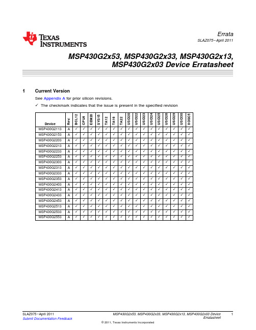
SLAZ075 – April 2011 Submit Documentation Feedback
MSP430G2x53, MSP430G2x33, MSP430G2x13, MSP430G2x03 Device
1
MSP430F2XX中文手册(加了标签) 10.通用串口

MSP430F2系列16位超低功耗单片机模块原理第10章通用串口界面Universal Serial Interface 版本: 1.5日期: 2007.5.原文: TI MSP430x2xxfamily.pdf翻译: 陈安都湖南长沙-中南大学编辑: DC 微控技术论坛版主注:以下文章是翻译TI MSP430x2xxfamily.pdf 文件中的部分内容。
由于我们翻译水平有限,有整理过程中难免有所不足或错误;所以以下内容只供参考.一切以原文为准。
详情请密切留意微控技术论坛。
Page 1 of 15通用串行接口模块(USI)提供与硬件模块的SPI和I2C串行通信。
本章讨论这两种模式。
USI模块包含在MSP420X20XX系列中。
主题10.1 USI的介绍10.2 USI的使用10.3 USI的寄存器10.1 USI的介绍USI模块提供支持同步串行通信的基本功能。
一般地,一个8、16位移位寄存器能用来输出数据流,少许的几条指令就可以执行串行通信。
另外,USI包含的内置硬件可以模拟SPI和I2C通信。
USI模块还包括中断,可以进一步减少串行通信的通用程序并且保持MSP430的低功耗特性。
USI模块的特性包括:支持三线SPI模式支持I2C模式可变的数据长度在LPM4方式下不需要内部时钟MSB或LSB指令可选在I2C模式下能控制SCL打开、停止监测在主机模式下的仲裁丢失监测可编程的时钟发生器可选择的钟极性和相位控制Page 2 of 15表10-1展示了SPI模式下的USI模块Page 3 of 15表10-2展示了I2C模式下的USI模块10.2 USI的操作USI模块主要由移位寄存器和位计数器组成,通过逻辑控制来支持SPI和I2C 通信。
USI的移位寄存器为USISR,通过软件直接控制数据的移入和移出。
位计数器计算采样位的数目以及在USICNTX位写零时设置USI中断标志位Page 4 of 15USIIFG。
以MSP430FW427为核心的远程数字水表设计[1]
![以MSP430FW427为核心的远程数字水表设计[1]](https://img.taocdn.com/s3/m/3ae9b0f9941ea76e58fa0414.png)
第22卷 第3期 2007年09月 西 南 科 技 大 学 学 报 Journal of South west University of Science and Technol ogy Vol .22No .3 Sep.2007 收稿日期:2007-03-07 基金项目:国家863计划项目(2005AA121520),西南科技大学重点科研基金项目(06zx2130)。
作者简介:周金治(1971-),男,硕士,讲师。
研究方向为网络体系结构与协议分析、DSP 技术及应用。
E -mail:zhoujinzhi@s wust .edu .cn 。
以MSP430F W427为核心的远程数字水表设计周金治 范富宏(西南科技大学信息工程学院 四川绵阳 621010)摘要:介绍了以M SP430为核心的低功耗远程数字水表设计。
以M SP430F W 427为微处理器,采集处理水流量信号;内嵌简化的T CP /I P 协议,采用CS8900A 的I/O SP ACE 模式实现数据的传输。
分析了LC 振荡电路检测流量信号的原理,给出了流量信号的检测、处理、显示及网络通信等模块的软硬件设计及流程。
实验表明,该水表具有低功耗、高精度等优点,测得的水流量既可本地显示,也可通过网络实现远程抄表。
关键词:数字水表 流量检测 MSP430F W 427微处理器 网络通信中图分类号:T M932 文献标识码:A 文章编号:1671-8755(2007)03-0079-04D esi gn of Rem ote D i g ita l W a ter M eter Ba sed on M SP 430F W 427Zhou J in 2zhi,Fan Fu 2hong(School of Infor m a tion Eng ineering,S outhw est U niversity of Science and Technology,M ianyang 621010,S ichuan,China )Abstract:The re mote l ow power consump ti on digital water meter based on MSP430was intr oduced .It can be used t o collect and p r ocess fluid signal with MSP430F W 427as MCU.Data 2trans porting was car 2ried out with I/O SP ACE mode of CS8900A by TCP /I P p r ot ocol .On analyzing the p rinci p le and p r ocess of fluid signals ’detecti on,hard ware and s oft w are design of signal ’s gathering,p r ocessing and net w ork communicati on were given .Experi m ental result shows that the water meter has the characteristic of l ow power and high p recisi on,the fluid signal can dis p lay l ocally and be accessed by I nternet .Key words:digital water meter;fluid signal detecting;MSP430F W 427MCU;net w ork communicati on随着电子通信与计算机网络技术的发展,远程抄表技术在水、电和煤气计量方面的应用已经逐渐发展起来,基于网络通信的水表已经成为水表的发展趋势。
MSP430F2XX中文手册(加了标签) 12.SPI 串行同步通讯模式
Page 4 of 14
MSP430 F2 系列超低功耗单片机模块原理 第 12 章 串行同步通讯模式 SPI
微控设计网
图12-2 通用串行通信接口主机和从机
图12-2说明了USCI在3线和4线模式下作为主机时的配置。当数据被送到传输数据缓冲器 UCxTXBUF时,USCI开始数据传送。当TX移位寄存器空了后,UCxTXBUF缓冲区的数据被传送到其 中, 在UCxSIMO上传送数据, 起始位是最高位还是最低位, 决定于UCMSB标志位的设置。 而UCxSOMI 上的数据在反向跳边沿下移入接收移位寄存器。当字符接收到之后,接收数据从RX移位寄存器 送入接收数据缓冲器UCxRXBUF,并且置位接收中断标志UCxRXIFG,表示接收/发送操作完成。 发送中断标志位UCxTXIFG被置位后,表明数据已从UCxTXBUF缓冲区进入TX移位寄存器, UCxTXBUF寄存器已经为发送新数据做好准备,但并不意味着传送和接收的完成。 为了在主机模式下接收USCI数据,数据必须事先写入UCxTXBUF,因为接收和发送操作不是 马上进行的。 4线SPI主机模式 在4线主机模式中,UCxSTE用来防止与其它主机相冲突并象表12-1描述的那样控制主机。当 UCxSTE处于主机不活动状态时: UCxSIMO 和 UCxCLK设置为输入,不再驱动总线。 出错位UCFE置位,表明在通讯的完整性上,使用者未按照规则操作。 内部状态被复位时,移位操作取消。 如果数据写入UCxTXBUF而主机通过UCxSTE位保持非工作状态, UCxSTE转换为主机工作状态, 数据立即被发送。如果一个正在工作的发送过程,因UCxSTE转换为主机不运行状态而取消时, 当UCxSTE转向主机运行状态时数据需要被重新写入UCxTXBUF。 UCxSTE输入信号不能应用3线主机 模式。 12.3.4 从机模式
MSP430F427IPM资料
元器件交易网IMPORTANT NOTICETexas Instruments Incorporated and its subsidiaries (TI) reserve the right to make corrections, modifications,enhancements, improvements, and other changes to its products and services at any time and to discontinueany product or service without notice. Customers should obtain the latest relevant information before placingorders and should verify that such information is current and complete. All products are sold subject to TI’s termsand conditions of sale supplied at the time of order acknowledgment.TI warrants performance of its hardware products to the specifications applicable at the time of sale inaccordance with TI’s standard warranty. T esting and other quality control techniques are used to the extent TIdeems necessary to support this warranty. Except where mandated by government requirements, testing of allparameters of each product is not necessarily performed.TI assumes no liability for applications assistance or customer product design. Customers are responsible fortheir products and applications using TI components. T o minimize the risks associated with customer productsand applications, customers should provide adequate design and operating safeguards.TI does not warrant or represent that any license, either express or implied, is granted under any TI patent right,copyright, mask work right, or other TI intellectual property right relating to any combination, machine, or processin which TI products or services are used. Information published by TI regarding third-party products or servicesdoes not constitute a license from TI to use such products or services or a warranty or endorsement thereof.Use of such information may require a license from a third party under the patents or other intellectual propertyof the third party, or a license from TI under the patents or other intellectual property of TI.Reproduction of information in TI data books or data sheets is permissible only if reproduction is withoutalteration and is accompanied by all associated warranties, conditions, limitations, and notices. Reproductionof this information with alteration is an unfair and deceptive business practice. TI is not responsible or liable forsuch altered documentation.Resale of TI products or services with statements different from or beyond the parameters stated by TI for thatproduct or service voids all express and any implied warranties for the associated TI product or service andis an unfair and deceptive business practice. TI is not responsible or liable for any such statements.Following are URLs where you can obtain information on other Texas Instruments products and applicationsolutions:Products ApplicationsAmplifiers Audio /audioData Converters Automotive /automotiveDSP Broadband /broadbandInterface Digital Control /digitalcontrolLogic Military /militaryPower Mgmt Optical Networking /opticalnetworkMicrocontrollers Security /securityTelephony /telephonyVideo & Imaging /videoWireless /wirelessMailing Address:Texas InstrumentsPost Office Box 655303 Dallas, Texas 75265Copyright 2004, Texas Instruments Incorporated。
MSP430F2XX中文手册(加了标签) 5.Flash块控制器
Page 1 of 18MSP430F2系列16位超低功耗单片机模块原理第5章 Flash 块控制器版本: 1.3日期: 2007.6.原文: TI MSP430x2xxfamily.pdf翻译: 余川编辑: DC 微控技术论坛版主注:以下文章是翻译TI MSP430x2xxfamily.pdf 文件中的部分内容。
由于我们翻译水平有限,有整理过程中难免有所不足或错误;所以以下内容只供参考.一切以原文为准。
详情请密切留意微控技术论坛。
第五章 Flash 存储控制器本章介绍了MSP430x2xx 系列单片机Flash 存储控制器的操作。
5.1 Flash 存储器的介绍Page 2 of 18 5.2 Flash 存储器的分段结构5.3 Flash 存储器的操作5.4 Flash 存储器的控制寄存器5.1 Flash 存储器的介绍MSP430 的F lash 存储器是可位/字节/字寻址和编程的存储器。
该模块由一个集成控制器来控制编程和擦除的操作。
控制器包括三个寄存器,一个时序发生器及一个提供编程/擦除电压的电压发生器。
MSP430 的F lash 存储器的特点有:● 产生内部编程电压● 可位/字节/字编程● 超低功耗操作● 支持段擦除和多段模块擦除F lash 存储器和控制器的结构框图如图5−1所示。
注意:F lash 写入和擦除操作期间的最小电压值V CC 应为2.2V 。
如果在操作期间V CC 低于2.2V ,写入或擦除的结果将是不确定的。
图5−1 F lash 存储器框图Page 3 of 185.2 Flash 存储器的分段结构MSP430 F lash 存储器分成多个段。
可对其进行单个位/字节/字的写入,但是最小的擦除单位是段。
F lash 存储器分为主存储器和信息存储器两部分,在操作上两者没有什么区别,程序代码和数据可以存储于任意部分。
两部分的区别在于段的大小和物理地址。
信息存储器有四个64字节的段,主存储器有两个或更多的512字节的段。
msp430中文资料_数据手册_参数
因此,寄存器操作执行时间是CPU时钟的一个周期。R0到R3中的四个寄存器分别是程序
计数器、堆栈指针、状msp430态寄存器和常量生成器。外围设备通过数据、地址和控制
总线连接到CPU,可以使用所有指令进行处理。指令msp430集指令集由51条指令组成,
有三种格式和七种地址模式。可对字和字节数据进行操作。表1显示了三种结构格式的示
例;地址模式为listedin表外 通过数据、地址和控制总线连接到CPU,可以使用所有指
令进行处理。有完 的模块描述,
MSP430x1xx家庭用户指南,literaturenumber
SLAU049。时钟系统由基本的时钟模块 ,包括对32768-Hz 表晶体 、内部数字
控msp430制振荡器(DCO)和高频晶体振荡器的 。基本 条模块的设计是为了 低
是一种超低功率混合msp430信号单片机,内置16位定时器和14个I/O引脚。典型的应用包
括捕捉模拟信号、将它们转换为数字值、然后处理数据并显示它们或将它们传输到主机
系统的传感器系统。独立射频传感器前端是另一个msp430应用领域1998年12月
MSP430x11xMIXED信号MICROCONTROLLERSSLAS196D 修订655303年9月20044邮政
列超msp430功率微控制器由几个不同的设备组成,其外围设备针对不同的应用。该体系
结构与五种低功耗模式相结合,优化后msp430可在便携式测量应用中延长电池寿命。该
设备具有强大的16位RISC CPU、16位寄存器和常量生成器,这些属性都具有最高的代码
效率。数控振荡器(DCO)允许从低功耗模式唤醒activemode在不到6 s。MSP430x11x系列
体谐振器 外部时钟的16位Timer_A ThreeCapture /比较RegistersD串行机上
- 1、下载文档前请自行甄别文档内容的完整性,平台不提供额外的编辑、内容补充、找答案等附加服务。
- 2、"仅部分预览"的文档,不可在线预览部分如存在完整性等问题,可反馈申请退款(可完整预览的文档不适用该条件!)。
- 3、如文档侵犯您的权益,请联系客服反馈,我们会尽快为您处理(人工客服工作时间:9:00-18:30)。
MSP430 的典型应用包括热量仪表、热水和冷水仪表、气体仪表和工业传感器系统。定时器支持额外 的计数器应用、射频位流操作、IrDA 和 M-Bus 通讯。
—1—
利尔达单片机技术有限公司 杭州市文二路 207 号文欣大厦 301 座 0571-88259199
TA –40°C to 85°C
MSP430xW42x引脚功能
输入/ 序
输出 号
说
明
64
电源正端,为SVS,上电复位,振荡器,FLL+,比较器A,I/O端口6和LCD电阻分
压电路供电,不能先于DVCC上电
62
电源负端,为SVS,上电复位,振荡器,FLL+,比较器A,I/O端口6供电,必须外
部连接到DVSS。内部连接到DVSS
1
数字供电电源正端,为除了由AVCC/AVSS供电的所有数字部分供电
可选型号 封装器件
64 脚 QFP 封装(PM) MSP430CW423IPM MSP430CW425IPM MSP430CW427IPM MSP430FW423IPM MSP430FW425IPM MSP430FW427IPM
MSP430xW42x 引脚
—2—
利尔达单片机技术有限公司 杭州市文二路 207 号文欣大厦 301 座 0571-88259199
TDI/TCLK
55
I 测试数据输入或测试时钟输入。芯片保护熔丝连接到TDI/TCLK
TDO/TDI
54 I/O 测试数据输出。TDO/TDI数据输出或者编程数据输入引脚
TMS
56
I 测试模式选择。TMS用于芯片编程和测试的输入端口
XIN
8
I 晶体振荡器XT1的输入端口。可以连接标准或者钟表晶振
XOUT
● 五种省电模式
● 6 微秒内从等待状态唤醒
● 锁频环,FLL+
● 16 位精简指令结构,125 纳秒指令时间周期
● 应用于水、热和气体仪表的体积流量测量的 SCAN-I/F 单元
● 带有三个捕捉/比较寄存器的 16 位定时器 Timer_A
● 带有五个捕捉/比较寄存器的 16 位定时器 Timer_A
外,LCD模块控制位可选择段线S18(注一) I/O 通用数字输入/输出/除端口功能外,LCD模块控制位可选择段线S17(注1) I/O 通用数字输入/输出/除端口功能外,LCD模块控制位可选择段线S16(注1) I/O 通用数字输入/输出/除端口功能外,LCD模块控制位可选择段线S15(注1) I/O 通用数字输入/输出/除端口功能外,LCD模块控制位可选择段线S14(注1) I/O 通用数字输入/输出/除端口功能外,LCD模块控制位可选择段线S13(注1) I/O 通用数字输入/输出/除端口功能外,LCD模块控制位可选择段线S12(注1) I/O 通用数字输入/输出/除端口功能外,LCD模块控制位可选择段线S11(注1) I/O 通用数字输入/输出/除端口功能外,LCD模块控制位可选择段线S10(注1) I/O 通用数字输入/输出/除端口功能外,LCD模块控制位可选择段线S9(注1) I/O 通用数字输入/输出/除端口功能外,LCD模块控制位可选择段线S8(注1) I/O 通用数字输入/输出/除端口功能外,LCD模块控制位可选择段线S7(注1) I/O 通用数字输入/输出/除端口功能外,LCD模块控制位可选择段线S6(注1) I/O 通用数字输入/输出/除端口功能外,LCD模块控制位可选择段线S5(注1) I/O 通用数字输入/输出/除端口功能外,LCD模块控制位可选择段线S4(注1) I/O 通用数字输入/输出/除端口功能外,LCD模块控制位可选择段线S3(注1) I/O 通用数字输入/输出/除端口功能外,LCD模块控制位可选择段线S2(注1) I/O 通用数字输入/输出/除端口功能外,LCD模块控制位可选择段线S1(注1) I/O 通用数字输入/输出/除端口功能外,LCD模块控制位可选择段线S0(注1) O 公共输出。COM0-3用于LCD底板-LCD I/O 通用数字输入/输出/ COM0-3用于LCD底板-LCD I/O 通用数字输入/输出/ COM0-3用于LCD底板-LCD I/O 通用数字输入/输出/ COM0-3用于LCD底板-LCD
47 I/O 通用数字输入/输出/比较器A输入 46 I/O 通用数字输入/输出/比较器A输入 45 I/O 通用数字输入/输出/Timer0_A2,捕获:CCI2A输入 /比较:Out2输出 44 I/O 通用数字输入/输出/Timer1_A1,捕获:CCI1A输入 /比较:Out1输出
—3—
利尔达单片机技术有限公司 杭州市文二路 207 号文欣大厦 301 座 0571-88259199
I/O 通用数字输入/输出/Timer1_A3,捕获:CCI3A输入 /比较:Out3输出端口/LCD模 块控制位可选择段线S22(注1)
I/O 通用数字输入/输出/Timer1_A4,捕获:CCI4A输入 /比较:Out4输出/LCD模块控 制位可选择段线S21(注1)
I/O 通用数字输入/输出/Timer1_A时钟输入/LCD模块控制位可选择段线S20(注1) I/O 通用数字输入/输出/比较器A输出/LCD模块控制位可选择段线S19(注1) I/O 通用数字输入/输出/来自内部时钟发生器的SIFCLKG时钟信号除端口和第二功能
P5.4/COM3
39
R03
40
P5.5/R13
41
P5.6/R23
42
P5.7/R33
43
P6.0/SIFCH059P6.1/SIFCH160
P6.2/SIFCH2
61
I/O 通用数字输入/输出/Timer1_A2,捕获:CCI2A输入 /比较:Out2输出除端口和第 二功能外,LCD模块控制位可选择段线S23(注1)
P2.2/TA1.2/S23 35
P2.3/TA1.3/S22 34
P2.4/TA1.4/S21 33
P2.5/TA1CLK/S20 32
P2.6/CAOUT/S19
31
P2.7/SIFCLKG/S18 30
P3.0/S17
29
P3.1/S16
28
P3.2/S15
27
P3.3/S14
26
P3.4/S13
6
I/O 通用数字输入/输出/SCAN-I/F,通道3,信号输入至比较器/上电复位、电源电压管
SVSIN
理的模拟输入
SIFCI
7
I SCAN IF输入到比较器
SIFCOM
11 I SCAN IF传感器公共端
RST/NMI
58 I 复位输入或非屏蔽中断输入端口
TCK
57
I 测试时钟。TCK是芯片编程和测试的输入端口
—4—
利尔达单片机技术有限公司 杭州市文二路 207 号文欣大厦 301 座 0571-88259199
P6.3/SIFCH3/
2
I/O 通用数字输入/输出/SCAN-I/F,通道3,传感器激励输出和信号输入,SCAN-I/F比
SIFCAOUT
较器输出
P6.4/SIFCI0
9
O 晶体振荡器XT1输出引脚
NOTE: I 当LCD模块控制位被置1,LCD功能自动选择,不用PxSEL位。
简要说明 处理单元
处理单元是基于兼容正交CPU指令集的。这种设计结构 对应用开发高度透明且易于编程。因此所有的操作,除了程 序流程指令,都是通过源操作数的7种寻址模式和目标操作数 的四种寻址模式的组合对寄存器操作进行的。
25
P3.5/S12
24
P3.6/S11
23
P3.7/S10
22
P4.0/S9
21
P4.1/S8
20
P4.2/S7
19
P4.3/S6
18
P4.4/S5
17
P4.5/S4
16
P4.6/S3
15
P4.7/S2
14
P5.0/S1
13
P5.1/S0
12
COM0
36
P5.2/COM1
37
P5.3/COM2
38
MSP430CW427:
32KB ROM 存储器, 1KB RAM
MSP430FW423:
8KB Flash 存储器, 512B RAM
MSP430FW425:
16KB Flash 存储器, 512B RAM
MSP430FW427:
32KB Flash 存储器, 1KB RAM
● 64 引脚 Quad Flat Pack(QFP)封装
I 第四个(最低)模拟LCD电平的输入端口-LCD(V5) I/O 通用数字输入/输出/第三高模拟LCD电平(V4或V3)输入端口-LCD I/O 通用数字输入/输出/第二高模拟LCD电平(V2)输入端口-LCD I/O 通用数字输入/输出/最高模拟LCD电平(V1)输入端口-LCD I/O 通用数字输入/输出/SCAN-I/F,通道0,传感器激励输出和信号输入 I/O 通用数字输入/输出/SCAN-I/F,通道1,传感器激励输出和信号输入 I/O 通用数字输入/输出/SCAN-I/F,通道2,传感器激励输出和信号输入
MSP430xW42x功能模块框图
引脚 引脚
AVCC
AVSS
DVCC DVSS SIFVSS P1.0/TA0.0 P1.1/TA0.0/ MCLK P1.2/TA0.1 P1.3/TA0.1/ SVSOUT P1.4/TA1.0 P1.5/TA0CLK/ ACLK P1.6/CA0 P1.7/CA1 P2.0/TA0.2 P2.1/TA1.1
3
I/O 通用数字输入/输出/SCAN-I/F,通道0,信号输入至比较器
P6.5/SIFCI1