Renormalization of Molecular Electronic Levels at Metal-Molecule Interfaces
“第17届凝聚态理论与统计物理学术会议”日程(初稿)

吴超(西安交通大学) 题目: The influence of local arrangements of oxygen adatoms on the energetics of O2 dissociation over Pt(111) 赵明文(山东大学) 题目: 新型碳材料结构设计和性能调控的理 论模型 李希茂(北京宏剑公司)(12:10-12:25) 题目: 第一原理计算材料的缺陷和掺杂特性
李文飞(南京大学) 题目: 蛋白质分子体系多尺度理论模拟
孙久勋(电子科技大学) 题目: Improvement of unified mobility model and electrical properties for organic diodes under dc and ac conditions
关丽(河北大学):Structural stability and electronic properties of two nonstoichiometric SrTiO3 phases
休息
报告厅 3(主题: 冷原子物理) 分会报告 ST3.3 主席:成 泽 教授(华中科技大学) (邀请报告) 周琦(香港中文大学) 题目:自旋轨道耦合下波色凝聚体的命运
主席:金国钧 教授(南京大学)
(邀请报告) 杨义峰(中国科学院物理研究所) (邀请报告) 孟胜(中国科学院物理研究所)
题目:重费米子物理中的演生现象
题目:Energy Conversion At Nanoscale
单分子综述-NATURE NANOTECHNOLOGY-Single-molecule junctions beyond electronic transport-2013
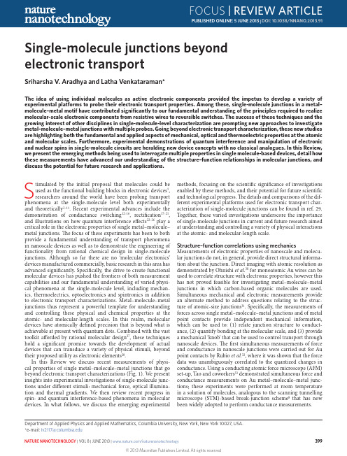
Stimulated by the initial proposal that molecules could be used as the functional building blocks in electronic devices 1, researchers around the world have been probing transport phenomena at the single-molecule level both experimentally and theoretically 2–11. Recent experimental advances include the demonstration of conductance switching 12–16, rectification 17–21, and illustrations on how quantum interference effects 22–26 play a critical role in the electronic properties of single metal–molecule–metal junctions. The focus of these experiments has been to both provide a fundamental understanding of transport phenomena in nanoscale devices as well as to demonstrate the engineering of functionality from rational chemical design in single-molecule junctions. Although so far there are no ‘molecular electronics’ devices manufactured commercially, basic research in this area has advanced significantly. Specifically, the drive to create functional molecular devices has pushed the frontiers of both measurement capabilities and our fundamental understanding of varied physi-cal phenomena at the single-molecule level, including mechan-ics, thermoelectrics, optoelectronics and spintronics in addition to electronic transport characterizations. Metal–molecule–metal junctions thus represent a powerful template for understanding and controlling these physical and chemical properties at the atomic- and molecular-length scales. I n this realm, molecular devices have atomically defined precision that is beyond what is achievable at present with quantum dots. Combined with the vast toolkit afforded by rational molecular design 27, these techniques hold a significant promise towards the development of actual devices that can transduce a variety of physical stimuli, beyond their proposed utility as electronic elements 28.n this Review we discuss recent measurements of physi-cal properties of single metal–molecule–metal junctions that go beyond electronic transport characterizations (Fig. 1). We present insights into experimental investigations of single-molecule junc-tions under different stimuli: mechanical force, optical illumina-tion and thermal gradients. We then review recent progress in spin- and quantum interference-based phenomena in molecular devices. I n what follows, we discuss the emerging experimentalSingle-molecule junctions beyond electronic transportSriharsha V. Aradhya and Latha Venkataraman*The id ea of using ind ivid ual molecules as active electronic components provid ed the impetus to d evelop a variety of experimental platforms to probe their electronic transport properties. Among these, single-molecule junctions in a metal–molecule–metal motif have contributed significantly to our fundamental understanding of the principles required to realize molecular-scale electronic components from resistive wires to reversible switches. The success of these techniques and the growing interest of other disciplines in single-molecule-level characterization are prompting new approaches to investigate metal–molecule–metal junctions with multiple probes. Going beyond electronic transport characterization, these new studies are highlighting both the fundamental and applied aspects of mechanical, optical and thermoelectric properties at the atomic and molecular scales. Furthermore, experimental demonstrations of quantum interference and manipulation of electronic and nuclear spins in single-molecule circuits are heralding new device concepts with no classical analogues. In this Review, we present the emerging methods being used to interrogate multiple properties in single molecule-based devices, detail how these measurements have advanced our understanding of the structure–function relationships in molecular junctions, and discuss the potential for future research and applications.methods, focusing on the scientific significance of investigations enabled by these methods, and their potential for future scientific and technological progress. The details and comparisons of the dif-ferent experimental platforms used for electronic transport char-acterization of single-molecule junctions can be found in ref. 29. Together, these varied investigations underscore the importance of single-molecule junctions in current and future research aimed at understanding and controlling a variety of physical interactions at the atomic- and molecular-length scale.Structure–function correlations using mechanicsMeasurements of electronic properties of nanoscale and molecu-lar junctions do not, in general, provide direct structural informa-tion about the junction. Direct imaging with atomic resolution as demonstrated by Ohnishi et al.30 for monoatomic Au wires can be used to correlate structure with electronic properties, however this has not proved feasible for investigating metal–molecule–metal junctions in which carbon-based organic molecules are used. Simultaneous mechanical and electronic measurements provide an alternate method to address questions relating to the struc-ture of atomic-size junctions 31. Specifically, the measurements of forces across single metal–molecule–metal junctions and of metal point contacts provide independent mechanical information, which can be used to: (1) relate junction structure to conduct-ance, (2) quantify bonding at the molecular scale, and (3) provide a mechanical ‘knob’ that can be used to control transport through nanoscale devices. The first simultaneous measurements of force and conductance in nanoscale junctions were carried out for Au point contacts by Rubio et al.32, where it was shown that the force data was unambiguously correlated to the quantized changes in conductance. Using a conducting atomic force microscope (AFM) set-up, Tao and coworkers 33 demonstrated simultaneous force and conductance measurements on Au metal–molecule–metal junc-tions; these experiments were performed at room temperature in a solution of molecules, analogous to the scanning tunnelling microscope (STM)-based break-junction scheme 8 that has now been widely adopted to perform conductance measurements.Department of Applied Physics and Applied Mathematics, Columbia University, New York, New York 10027, USA. *e-mail: lv2117@DOI: 10.1038/NNANO.2013.91These initial experiments relied on the so-called static mode of AFM-based force spectroscopy, where the force on the canti-lever is monitored as a function of junction elongation. I n this method the deflection of the AFM cantilever is directly related to the force on the junction by Hooke’s law (force = cantilever stiff-ness × cantilever deflection). Concurrently, advances in dynamic force spectroscopy — particularly the introduction of the ‘q-Plus’ configuration 34 that utilizes a very stiff tuning fork as a force sen-sor — are enabling high-resolution measurements of atomic-size junctions. In this technique, the frequency shift of an AFM cantilever under forced near-resonance oscillation is measuredas a function of junction elongation. This frequency shift can be related to the gradient of the tip–sample force. The underlying advantage of this approach is that frequency-domain measure-ments of high-Q resonators is significantly easier to carry out with high precision. However, in contrast to the static mode, recover-ing the junction force from frequency shifts — especially in the presence of dissipation and dynamic structural changes during junction elongation experiments — is non-trivial and a detailed understanding remains to be developed 35.The most basic information that can be determined throughsimultaneous measurement of force and conductance in metalThermoelectricsSpintronics andMechanicsOptoelectronicsHotColdFigure 1 | Probing multiple properties of single-molecule junctions. phenomena in addition to demonstrations of quantum mechanical spin- and interference-dependent transport concepts for which there are no analogues in conventional electronics.contacts is the relation between the measured current and force. An experimental study by Ternes et al.36 attempted to resolve a long-standing theoretical prediction 37 that indicated that both the tunnelling current and force between two atomic-scale metal contacts scale similarly with distance (recently revisited by Jelinek et al.38). Using the dynamic force microscopy technique, Ternes et al. effectively probed the interplay between short-range forces and conductance under ultrahigh-vacuum conditions at liquid helium temperatures. As illustrated in Fig. 2a, the tunnel-ling current through the gap between the metallic AFM probe and the substrate, and the force on the cantilever were recorded, and both were found to decay exponentially with increasing distance with nearly the same decay constant. Although an exponential decay in current with distance is easily explained by considering an orbital overlap of the tip and sample wavefunctions through a tunnel barrier using Simmons’ model 39, the exponential decay in the short-range forces indicated that perhaps the same orbital controlled the interatomic short-range forces (Fig. 2b).Using such dynamic force microscopy techniques, research-ers have also studied, under ultrahigh-vacuum conditions, forces and conductance across junctions with diatomic adsorbates such as CO (refs 40,41) and more recently with fullerenes 42, address-ing the interplay between electronic transport, binding ener-getics and structural evolution. I n one such experiment, Tautz and coworkers 43 have demonstrated simultaneous conduct-ance and stiffness measurements during the lifting of a PTCDA (3,4,9,10-perylene-tetracarboxylicacid-dianhydride) molecule from a Ag(111) substrate using the dynamic mode method with an Ag-covered tungsten AFM tip. The authors were able to follow the lifting process (Fig. 2c,d) monitoring the junction stiffness as the molecule was peeled off the surface to yield a vertically bound molecule, which could also be characterized electronically to determine the conductance through the vertical metal–molecule–metal junction with an idealized geometry. These measurements were supported by force field-based model calculations (Fig. 2c and dashed black line in Fig. 2d), presenting a way to correlate local geometry to the electronic transport.Extending the work from metal point contacts, ambient meas-urements of force and conductance across single-molecule junc-tions have been carried out using the static AFM mode 33. These measurements allow correlation of the bond rupture forces with the chemistry of the linker group and molecular backbone. Single-molecule junctions are formed between a Au-metal sub-strate and a Au-coated cantilever in an environment of molecules. Measurements of current through the junction under an applied bias determine conductance, while simultaneous measurements of cantilever deflection relate to the force applied across the junction as shown in Fig. 2e. Although measurements of current throughzF zyxCantileverIVabConductance G (G 0)1 2 3Tip–sample distance d (Å)S h o r t -r a n g e f o r c e F z (n N )10−310−210−11110−110−210−3e10−410−210C o n d u c t a n c e (G 0)Displacement86420Force (nN)0.5 nm420−2F o r c e (n N )−0.4−0.200.20.4Displacement (nm)SSfIncreasing rupture forcegc(iv)(i)(iii)(ii)Low HighCounts d9630−3d F /d z (n N n m −1)(i)(iv)(iii)(ii)A p p r o a chL i ft i n g110−210−4G (2e 2/h )2051510z (Å)H 2NNH 2H 2NNH 2NNFigure 2 | Simultaneous measurements of electronic transport and mechanics. a , A conducting AFM set-up with a stiff probe (shown schematically) enabled the atomic-resolution imaging of a Pt adsorbate on a Pt(111) surface (tan colour topography), before the simultaneous measurement of interatomic forces and currents. F z , short-range force. b , Semilogarithmic plot of tunnelling conductance and F z measured over the Pt atom. A similar decay constant for current and force as a function of interatomic distance is seen. The blue dashed lines are exponential fits to the data. c , Structural snapshots showing a molecular mechanics simulation of a PTCDA molecule held between a Ag substrate and tip (read right to left). It shows the evolution of the Ag–PTCDA–Ag molecular junction as a function of tip–surface distance. d , Upper panel shows experimental stiffness (d F /d z ) measurements during the lifting process performed with a conducting AFM. The calculated values from the simulation are overlaid (dashed black line). Lower panel shows simultaneously measured conductance (G ). e , Simultaneously measured conductance (red) and force (blue) measurements showing evolution of a molecular junction as a function of junction elongation. A Au point contact is first formed, followed by the formation of a single-molecule junction, which then ruptures on further elongation. f , A two-dimensional histogram of thousands of single-molecule junctionrupture events (for 1,4-bis(methyl sulphide) butane; inset), constructed by redefining the rupture location as the zero displacement point. The most frequently measured rupture force is the drop in force (shown by the double-headed arrow) at the rupture location in the statistically averaged force trace (overlaid black curve). g , Beyond the expected dependence on the terminal group, the rupture force is also sensitive to the molecular backbone, highlighting the interplay between chemical structure and mechanics. In the case of nitrogen-terminated molecules, rupture force increases fromaromatic amines to aliphatic amines and the highest rupture force is for molecules with pyridyl moieties. Figure reproduced with permission from: a ,b , ref. 36, © 2011 APS; c ,d , ref. 43, © 2011 APS.DOI: 10.1038/NNANO.2013.91such junctions are easily accomplished using standard instru-mentation, measurements of forces with high resolution are not straightforward. This is because a rather stiff cantilever (with a typical spring constant of ~50 N m−1) is typically required to break the Au point contact that is first formed between the tip and sub-strate, before the molecular junctions are created. The force reso-lution is then limited by the smallest deflection of the cantilever that can be measured. With a custom-designed system24 our group has achieved a cantilever displacement resolution of ~2 pm (com-pare with Au atomic diameter of ~280 pm) using an optical detec-tion scheme, allowing the force noise floor of the AFM set-up to be as low as 0.1 nN even with these stiff cantilevers (Fig. 2e). With this system, and a novel analysis technique using two-dimensional force–displacement histograms as illustrated in Fig. 2f, we have been able to systematically probe the influence of the chemical linker group44,45 and the molecular backbone46 on single-molecule junction rupture force as illustrated in Fig. 2g.Significant future opportunities with force measurements exist for investigations that go beyond characterizations of the junc-tion rupture force. In two independent reports, one by our group47 and another by Wagner et al.48, force measurements were used to quantitatively measure the contribution of van der Waals interac-tions at the single-molecule level. Wagner et al. used the stiffness data from the lifting of PTCDA molecules on a Au(111) surface, and fitted it to the stiffness calculated from model potentials to estimate the contribution of the various interactions between the molecule and the surface48. By measuring force and conductance across single 4,4’-bipyridine molecules attached to Au electrodes, we were able to directly quantify the contribution of van der Waals interactions to single-molecule-junction stiffness and rupture force47. These experimental measurements can help benchmark the several theoretical frameworks currently under development aiming to reliably capture van der Waals interactions at metal/ organic interfaces due to their importance in diverse areas includ-ing catalysis, electronic devices and self-assembly.In most of the experiments mentioned thus far, the measured forces were typically used as a secondary probe of junction prop-erties, instead relying on the junction conductance as the primary signature for the formation of the junction. However, as is the case in large biological molecules49, forces measured across single-mol-ecule junctions can also provide the primary signature, thereby making it possible to characterize non-conducting molecules that nonetheless do form junctions. Furthermore, molecules pos-sess many internal degrees of motion (including vibrations and rotations) that can directly influence the electronic transport50, and the measurement of forces with such molecules can open up new avenues for mechanochemistry51. This potential of using force measurements to elucidate the fundamentals of electronic transport and binding interactions at the single-molecule level is prompting new activity in this area of research52–54. Optoelectronics and optical spectroscopyAddressing optical properties and understanding their influence on electronic transport in individual molecular-scale devices, col-lectively referred to as ‘molecular optoelectronics’, is an area with potentially important applications55. However, the fundamental mismatch between the optical (typically, approximately at the micrometre scale) and molecular-length scales has historically presented a barrier to experimental investigations. The motiva-tions for single-molecule optoelectronic studies are twofold: first, optical spectroscopies (especially Raman spectroscopy) could lead to a significantly better characterization of the local junction structure. The nanostructured metallic electrodes used to real-ize single-molecule junctions are coincidentally some of the best candidates for local field enhancement due to plasmons (coupled excitations of surface electrons and incident photons). This there-fore provides an excellent opportunity for understanding the interaction of plasmons with molecules at the nanoscale. Second, controlling the electronic transport properties using light as an external stimulus has long been sought as an attractive alternative to a molecular-scale field-effect transistor.Two independent groups have recently demonstrated simulta-neous optical and electrical measurements on molecular junctions with the aim of providing structural information using an optical probe. First, Ward et al.56 used Au nanogaps formed by electromi-gration57 to create molecular junctions with a few molecules. They then irradiated these junctions with a laser operating at a wavelength that is close to the plasmon resonance of these Au nanogaps to observe a Raman signal attributable to the molecules58 (Fig. 3a). As shown in Fig. 3b, they observed correlations between the intensity of the Raman features and magnitude of the junction conductance, providing direct evidence that Raman signatures could be used to identify junction structures. They later extended this experimental approach to estimate vibrational and electronic heating in molecu-lar junctions59. For this work, they measured the ratio of the Raman Stokes and anti-Stokes intensities, which were then related to the junction temperature as a function of the applied bias voltage. They found that the anti-Stokes intensity changed with bias voltage while the Stokes intensity remained constant, indicating that the effective temperature of the Raman-active mode was affected by passing cur-rent through the junction60. Interestingly, Ward et al. found that the vibrational mode temperatures exceeded several hundred kelvin, whereas earlier work by Tao and co-workers, who used models for junction rupture derived from biomolecule research, had indicated a much smaller value (~10 K) for electronic heating61. Whether this high temperature determined from the ratio of the anti-Stokes to Stokes intensities indicates that the electronic temperature is also similarly elevated is still being debated55, however, one can definitely conclude that such measurements under a high bias (few hundred millivolts) are clearly in a non-equilibrium transport regime, and much more research needs to be performed to understand the details of electronic heating.Concurrently, Liu et al.62 used the STM-based break-junction technique8 and combined this with Raman spectroscopy to per-form simultaneous conductance and Raman measurements on single-molecule junctions formed between a Au STM tip and a Au(111) substrate. They coupled a laser to a molecular junction as shown in Fig. 3c with a 4,4’-bipyridine molecule bridging the STM tip (top) and the substrate (bottom). Pyridines show clear surface-enhanced Raman signatures on metal58, and 4,4’-bipy-ridine is known to form single-molecule junctions in the STM break-junction set-up8,15. Similar to the study of Ward et al.56, Liu et al.62 found that conducting molecular junctions had a Raman signature that was distinct from the broken molecu-lar junctions. Furthermore, the authors studied the spectra of 4,4’-bipyridine at different bias voltages, ranging from 10 to 800 mV, and reported a reversible splitting of the 1,609 cm–1 peak (Fig. 3d). Because this Raman signature is due to a ring-stretching mode, they interpreted this splitting as arising from the break-ing of the degeneracy between the rings connected to the source and drain electrodes at high biases (Fig. 3c). Innovative experi-ments such as these have demonstrated that there is new physics to be learned through optical probing of molecular junctions, and are initiating further interest in understanding the effect of local structure and vibrational effects on electronic transport63. Experiments that probe electroluminescence — photon emis-sion induced by a tunnelling current — in these types of molec-ular junction can also offer insight into structure–conductance correlations. Ho and co-workers have demonstrated simultaneous measurement of differential conductance and photon emissionDOI: 10.1038/NNANO.2013.91from individual molecules at a submolecular-length scale using an STM 64,65. Instead of depositing molecules directly on a metal sur-face, they used an insulating layer to decouple the molecule from the metal 64,65 (Fig. 3e). This critical factor, combined with the vac-uum gap with the STM tip, ensures that the metal electrodes do not quench the radiated photons, and therefore the emitted photons carry molecular fingerprints. Indeed, the experimental observation of molecular electroluminescence of C 60 monolayers on Au(110) by Berndt et al.66 was later attributed to plasmon-mediated emission of the metallic electrodes, indirectly modulated by the molecule 67. The challenge of finding the correct insulator–molecule combination and performing the experiments at low temperature makes electro-luminescence relatively uncommon compared with the numerous Raman studies; however, progress is being made on both theoretical and experimental fronts to understand and exploit emission pro-cesses in single-molecule junctions 68.Beyond measurements of the Raman spectra of molecular junctions, light could be used to control transport in junctions formed with photochromic molecular backbones that occur in two (or more) stable and optically accessible states. Some common examples include azobenzene derivatives, which occur in a cis or trans form, as well as diarylene compounds that can be switched between a conducting conjugated form and a non-conducting cross-conjugated form 69. Experiments probing the conductance changes in molecular devices formed with such compounds have been reviewed in depth elsewhere 70,71. However, in the single-mol-ecule context, there are relatively few examples of optical modula-tion of conductance. To a large extent, this is due to the fact that although many molecular systems are known to switch reliably in solution, contact to metallic electrodes can dramatically alter switching properties, presenting a significant challenge to experi-ments at the single-molecule level.Two recent experiments have attempted to overcome this chal-lenge and have probed conductance changes in single-molecule junctions while simultaneously illuminating the junctions with visible light 72,73. Battacharyya et al.72 used a porphyrin-C 60 ‘dyad’ molecule deposited on an indium tin oxide (I TO) substrate to demonstrate the light-induced creation of an excited-state mol-ecule with a different conductance. The unconventional transpar-ent ITO electrode was chosen to provide optical access while also acting as a conducting electrode. The porphyrin segment of the molecule was the chromophore, whereas the C 60 segment served as the electron acceptor. The authors found, surprisingly, that the charge-separated molecule had a much longer lifetime on ITO than in solution. I n the break-junction experiments, the illuminated junctions showed a conductance feature that was absent without1 μm Raman shift (cm –1)1,609 cm –1(–)Source 1,609 cm–1Drain (+)Low voltage High voltageMgPNiAl(110)STM tip (Ag)VacuumThin alumina 1.4 1.5 1.6 1.701020 3040200400Photon energy (eV)3.00 V 2.90 V 2.80 V 2.70 V 2.60 V2.55 V 2.50 VP h o t o n c o u n t s (a .u .)888 829 777731Wavelength (nm)Oxideacebd f Raman intensity (CCD counts)1,5001,00050000.40.30.20.10.01,590 cm −11,498 cm −1d I /d V (μA V –1)1,609 cm –11,631 cm–11 μm1 μmTime (s)Figure 3 | Simultaneous studies of optical effects and transport. a , A scanning electron micrograph (left) of an electromigrated Au junction (light contrast) lithographically defined on a Si substrate (darker contrast). The nanoscale gap results in a ‘hot spot’ where Raman signals are enhanced, as seen in the optical image (right). b , Simultaneously measured differential conductance (black, bottom) and amplitudes of two molecular Raman features (blue traces, middle and top) as a function of time in a p-mercaptoaniline junction. c , Schematic representation of a bipyridine junction formed between a Au STM tip and a Au(111) substrate, where the tip enhancement from the atomically sharp STM tip results in a large enhancement of the Raman signal. d , The measured Raman spectra as a function of applied bias indicate breaking of symmetry in the bound molecule. e , Schematic representation of a Mg-porphyrin (MgP) molecule sandwiched between a Ag STM tip and a NiAl(110) substrate. A subnanometre alumina insulating layer is a key factor in measuring the molecular electroluminescence, which would otherwise be overshadowed by the metallic substrate. f , Emission spectra of a single Mg-porphyrin molecule as a function of bias voltage (data is vertically offset for clarity). At high biases, individual vibronic peaks become apparent. The spectra from a bare oxide layer (grey) is shown for reference. Figure reproduced with permission from: a ,b , ref. 56, © 2008 ACS; c ,d , ref. 62, © 2011 NPG; e ,f , ref. 65, © 2008 APS.DOI: 10.1038/NNANO.2013.91light, which the authors assigned to the charge-separated state. In another approach, Lara-Avila et al.73 have reported investigations of a dihydroazulene (DHA)/vinylheptafulvene (VHF) molecule switch, utilizing nanofabricated gaps to perform measurements of Au–DHA–Au single-molecule junctions. Based on the early work by Daub et al.74, DHA was known to switch to VHF under illumina-tion by 353-nm light and switch back to DHA thermally. In three of four devices, the authors observed a conductance increase after irradiating for a period of 10–20 min. In one of those three devices, they also reported reversible switching after a few hours. Although much more detailed studies are needed to establish the reliability of optical single-molecule switches, these experiments provide new platforms to perform in situ investigations of single-molecule con-ductance under illumination.We conclude this section by briefly pointing to the rapid pro-gress occurring in the development of optical probes at the single-molecule scale, which is also motivated by the tremendous interest in plasmonics and nano-optics. As mentioned previously, light can be coupled into nanoscale gaps, overcoming experimental chal-lenges such as local heating. Banerjee et al.75 have exploited these concepts to demonstrate plasmon-induced electrical conduction in a network of Au nanoparticles that form metal–molecule–metal junctions between them (Fig. 3f). Although not a single-molecule measurement, the control of molecular conductance through plas-monic coupling can benefit tremendously from the diverse set of new concepts under development in this area, such as nanofabri-cated transmission lines 76, adiabatic focusing of surface plasmons, electrical excitation of surface plasmons and nanoparticle optical antennas. The convergence of plasmonics and electronics at the fundamental atomic- and molecular-length scales can be expected to provide significant opportunities for new studies of light–mat-ter interaction 77–79.Thermoelectric characterization of single-molecule junctions Understanding the electronic response to heating in a single-mole-cule junction is not only of basic scientific interest; it can have a tech-nological impact by improving our ability to convert wasted heat into usable electricity through the thermoelectric effect, where a temper-ature difference between two sides of a device induces a voltage drop across it. The efficiency of such a device depends on its thermopower (S ; also known as the Seebeck coefficient), its electric and thermal conductivity 80. Strategies for increasing the efficiency of thermoelec-tric devices turned to nanoscale devices a decade ago 81, where one could, in principle, increase the electronic conductivity and ther-mopower while independently minimizing the thermal conductiv-ity 82. This has motivated the need for a fundamental understandingof thermoelectrics at the single-molecule level 83, and in particular, the measurement of the Seebeck coefficient in such junctions. The Seebeck coefficient, S = −(ΔV /ΔT )|I = 0, determines the magnitude of the voltage developed across the junction when a temperature dif-ference ΔT is applied, as illustrated in Fig. 4a; this definition holds both for bulk devices and for single-molecule junctions. If an addi-tional external voltage ΔV exists across the junction, then the cur-rent I through the junction is given by I = G ΔV + GS ΔT where G is the junction conductance 83. Transport through molecular junctions is typically in the coherent regime where conductance, which is pro-portional to the electronic transmission probability, is given by the Landauer formula 84. The Seebeck coefficient at zero applied voltage is then related to the derivative of the transmission probability at the metal Fermi energy (in the off-resonance limit), with, S = −∂E ∂ln( (E ))π2k 2B T E 3ewhere k B is the Boltzmann constant, e is the charge of the electron, T (E ) is the energy-dependent transmission function and E F is the Fermi energy. When the transmission function for the junction takes on a simple Lorentzian form 85, and transport is in the off-resonance limit, the sign of S can be used to deduce the nature of charge carriers in molecular junctions. In such cases, a positive S results from hole transport through the highest occupied molecu-lar orbital (HOMO) whereas a negative S indicates electron trans-port through the lowest unoccupied molecular orbital (LUMO). Much work has been performed on investigating the low-bias con-ductance of molecular junctions using a variety of chemical linker groups 86–89, which, in principle, can change the nature of charge carriers through the junction. Molecular junction thermopower measurements can thus be used to determine the nature of charge carriers, correlating the backbone and linker chemistry with elec-tronic aspects of conduction.Experimental measurements of S and conductance were first reported by Ludoph and Ruitenbeek 90 in Au point contacts at liquid helium temperatures. This work provided a method to carry out thermoelectric measurements on molecular junctions. Reddy et al.91 implemented a similar technique in the STM geome-try to measure S of molecular junctions, although due to electronic limitations, they could not simultaneously measure conductance. They used thiol-terminated oligophenyls with 1-3-benzene units and found a positive S that increased with increasing molecular length (Fig. 4b). These pioneering experiments allowed the iden-tification of hole transport through thiol-terminated molecular junctions, while also introducing a method to quantify S from statistically significant datasets. Following this work, our group measured the thermoelectric current through a molecular junction held under zero external bias voltage to determine S and the con-ductance through the same junction at a finite bias to determine G (ref. 92). Our measurements showed that amine-terminated mol-ecules conduct through the HOMO whereas pyridine-terminatedmolecules conduct through the LUMO (Fig. 4b) in good agree-ment with calculations.S has now been measured on a variety of molecular junctionsdemonstrating both hole and electron transport 91–95. Although the magnitude of S measured for molecular junctions is small, the fact that it can be tuned by changing the molecule makes these experiments interesting from a scientific perspective. Future work on the measurements of the thermal conductance at the molecu-lar level can be expected to establish a relation between chemical structure and the figure of merit, which defines the thermoelec-tric efficiencies of such devices and determines their viability for practical applications.SpintronicsWhereas most of the explorations of metal–molecule–metal junc-tions have been motivated by the quest for the ultimate minia-turization of electronic components, the quantum-mechanical aspects that are inherent to single-molecule junctions are inspir-ing entirely new device concepts with no classical analogues. In this section, we review recent experiments that demonstrate the capability of controlling spin (both electronic and nuclear) in single-molecule devices 96. The early experiments by the groups of McEuen and Ralph 97, and Park 98 in 2002 explored spin-depend-ent transport and the Kondo effect in single-molecule devices, and this topic has recently been reviewed in detail by Scott and Natelson 99. Here, we focus on new types of experiment that are attempting to control the spin state of a molecule or of the elec-trons flowing through the molecular junction. These studies aremotivated by the appeal of miniaturization and coherent trans-port afforded by molecular electronics, combined with the great potential of spintronics to create devices for data storage and quan-tum computation 100. The experimental platforms for conducting DOI: 10.1038/NNANO.2013.91。
超分子化学领域获得诺贝尔化学奖的学者及其主要贡献

超分子化学是化学领域中的一个重要分支,其研究对象是由分子通过非共价键相互作用组装而成的超分子结构。
超分子化学的研究对于理解生命现象、设计新型功能材料以及推动化学领域的发展具有重要意义。
多位杰出的科学家在超分子化学领域取得了突出成就,其中部分学者凭借其卓越的贡献获得了诺贝尔化学奖的殊荣。
本文将介绍超分子化学领域获得诺贝尔化学奖的学者及其主要贡献。
一、 Jean-Marie Lehn1. Jean-Marie Lehn是法国著名的化学家,他于1987年获得诺贝尔化学奖,主要是因为他在超分子化学领域的杰出贡献。
2. Lehn教授是超分子化学的开创者之一,他提出了分子识别和主客体相互作用的概念,成功地设计和构建了一系列具有特定功能的超分子结构。
3. 他的贡献不仅在理论方面,还在实验技术和方法上有重要突破,为超分子化学的发展注入了新的活力。
二、 Donald J. Cram1. Donald J. Cram是美国著名的化学家,他于1987年与Jean-Marie Lehn一同获得诺贝尔化学奖,是因为他在超分子化学领域的重要贡献。
2. Cram教授主要是通过设计和合成具有特定空腔结构的分子,实现了对其他分子的特异性识别,为超分子化学的发展开辟了新的方向。
3. 他的研究成果不仅在化学领域产生了深远影响,在生命科学和材料科学等领域也具有重要意义,促进了科学技术的进步。
三、 Jean-Pierre Sauvage1. Jean-Pierre Sauvage是法国著名的化学家,他于2016年获得诺贝尔化学奖,是因为他在超分子化学领域的开拓性研究成果。
2. Sauvage教授在超分子化学中提出了“机械化学”这一新概念,通过设计和合成具有机械运动功能的分子结构,实现了分子的机械运动和控制。
3. 他的研究成果为分子机器的设计与制备提供了重要思路,为纳米技术和生物医药领域的发展带来了新的机遇和挑战。
四、 Fraser Stoddart1. Fraser Stoddart是英国著名的化学家,他于2016年与Jean-Pierre Sauvage一同获得诺贝尔化学奖,是因为他在超分子化学领域的开创性工作。
瑞年NO

·
诺贝尔, 诺贝尔, 生于瑞典的斯德哥尔摩。 诺贝尔一生致力于炸药的研究,在硝化甘油的研究 方面取得了重大成就。他一生共获得技术发明专利355项, 方面取得了重大成就。他一生共获得技术发明专利355项, 并在欧美等五大洲20个国家开设了约100家公司和工厂, 并在欧美等五大洲20个国家开设了约100家公司和工厂, 积累了巨额财富。 1896年12月10日,诺贝尔在意大利逝世,逝世的前一 1896年12月10日,诺贝尔在意大利逝世,逝世的前一 年,他留下了遗嘱,设立诺贝尔奖 。 每次诺贝尔奖的发奖仪式都是下午举行,这是因为诺 贝尔是1896年12月10日下午4 30去世的 贝尔是1896年12月10日下午4:30去世的 .
“NO”与诺贝尔生理医学奖 3位科学家 28年呕心沥血
因研究“NO” 因研究“NO”终获诺贝尔生理医学奖
理医学奖 一氧化氮, 一氧化氮, 可输张血管、 可输张血管、防治心脑血管疾病
NO:3位科学家共同的重大发现
美国加州大学洛杉矶分校药理学教授,药学院院长伊 格纳罗(Ignarro)博士与佛契哥特(Furchgott)、穆拉德 (Murad)另外两位美国科学家研究发现:舒张血管平滑肌 舒张血管平滑肌 的神奇物质不是科学界猜测已久的蛋白质类大分子, 的神奇物质不是科学界猜测已久的蛋白质类大分子,而是人 体中的一氧化氮(Nitric Oxide)。 体中的一氧化氮
获得过诺贝尔奖的著名人物亨利•杜 Nhomakorabea 亨利 杜南
居里夫人
爱因斯坦
马可尼
纳尔逊•曼德拉 纳尔逊 曼德拉
诺贝尔奖医学奖获奖情况
诺贝尔医学奖早期获奖者
白喉的发现者、疟疾的发现者、结核 杆菌的发现者
诺贝尔医学奖中期获奖者
分子动力学模拟的英文

分子动力学模拟的英文Molecular dynamics simulation is a computational method used to study the physical movements of atoms and molecules. It involves solving Newton's equations of motion for a system of interacting particles, typically using numerical methods. This technique allows researchers to gain insights into the dynamic behavior of materials, biological systems, and other complex systems at atomic or molecular scales.The fundamental principle of molecular dynamics simulation is to represent the system of interest as a collection of interacting particles. These particles can be atoms, molecules, or clusters of atoms/molecules, depending on the level of detail required for the simulation. The interactions between particles are typically describedusing force fields, which are mathematical functions that describe the potential energy of the system as a functionof the positions and orientations of the particles.The simulation process begins with the selection of aninitial configuration for the system. This can be obtained from experimental data, or it can be generated randomly or using specific algorithms. Once the initial configurationis set, the forces acting on each particle are calculated using the force field. These forces are then used to compute the accelerations of the particles according to Newton's second law of motion. The velocities and positions of the particles are then updated using these accelerations, typically using a time-stepping algorithm such as theVerlet algorithm.The simulation continues by iterating this process over time, allowing the system to evolve dynamically. As the simulation proceeds, the particles move and interact with each other, leading to changes in the system's structureand properties. By monitoring these changes, researcherscan gain insights into the dynamic behavior of the system and how it responds to external perturbations or changes in conditions.Molecular dynamics simulations can be used to study a wide range of systems and phenomena. In materials science,they can be used to understand the atomic-scale mechanisms underlying material properties such as mechanical strength, thermal conductivity, and electrical conductivity. In biology, they can be used to study the dynamics of proteins, nucleic acids, and other biomolecules, revealing insights into their function and interactions with other molecules.In addition to providing fundamental understanding of these systems, molecular dynamics simulations can also be used to predict and design new materials or molecules with desired properties. For example, they can be used to screen potential drug candidates or optimize the performance of materials for specific applications.However, it is important to note that molecular dynamics simulations have limitations. The accuracy of the results depends on the quality of the force field used to describe the interactions between particles. While manyforce fields have been developed and validated fordifferent types of systems, they may not always accurately represent the complex interactions that occur in real systems. Furthermore, molecular dynamics simulations arecomputationally intensive and may require significant resources to run, especially for large systems or long simulation times.Despite these limitations, molecular dynamics simulations have become a valuable tool in many fields of science and engineering. They provide a unique means to study the dynamic behavior of complex systems at atomic or molecular scales, complementing experimental techniques and enabling the discovery of new materials and molecules with improved properties.。
高效毛细管电泳-安培法同时检测感冒药中的扑尔敏、扑热息痛和维生素C
Ù扑
Ù 维生素
∗
Ù
Ù∀
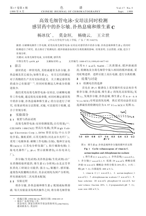
图 强力 ς χ 银翘片中扑尔敏 扑热息痛 维生素 Χ 的 ΧΕ -Ε Χ 图
Φιγ Ε λεχτρο ηερογ ρα σ οφ χηλορ ηενα ινε
αλεατε αχετα ινο ηεν
ϖιτα ιν Χ
ιν Θιανγ λι Ψινθιαο χονταινινγ ς χ ταβλετ 丙二醇的体积分数 检测条件同图 ∀
极
江苏电分析仪器厂 铂片辅助电极 上
海 电光器件厂
型示波极谱仪 山东电讯七
厂∀
扑尔敏 生化试剂 及扑热息痛 生化试剂 由广
东药物检验所提供 维生素 分析纯 由北京芳草
医药化工研制公司提供 强力 银翘片 感冒敏
速效伤风胶囊购自药店 其余试剂均为国产分析纯
所有溶液均用二次双蒸水配制∀
图 维生素 Χ 扑热息痛和扑尔敏的循环伏安图
的成分已有报道 ∗ 但同时检测这几种成分的报
检测电位的选择
道很少∀ 我们采用高效毛细管电泳安培法 以碳糊电极
作工作电极 通过优化实验参数 对同时测定感冒药 中的扑尔敏 扑热息痛和维生素 的方法进行了研 究∀结果表明该方法简便 灵敏 可直接用于检测 适
首先在 极谱仪上采用循环伏安法初步考
察扑尔敏 扑热息痛 维生素 的氧化还原情况 见
∀ 其余
样品测定
将样品 种感冒药 分别研磨成粉状 充分混
合∀ 准确称取一定量的样品粉末 加入适量水 在超
声波发生器内振荡
后 加水定容 临用前经
Λ 的滤膜过滤∀样品按照外标法进行定量 并
在其中添加标准液进行回收实验 结果见表 ∀ 由表
可见 样品的回收率为
计算凝聚态物理介绍

.
• In the opposite, Hohenberg-Kohn demonstrated that there is
only one external potential
to yield a given ground state
charge density.
If we assume then
Kohn-Sham Theorem (1965)
计算 凝聚态物理介绍
内容提要
一、计算(凝聚态)物理简介 二、精确对角化方法 三、数值重整化群:
从 K.G.Wilson 到 S.R.White 四、蒙特卡罗模拟 五、符号计算
一、计算(凝聚态)物理简介
1. 计算物理、计算凝聚态物理
2. 计算物理的发展 (1)早期的推动 (2)计算物理方法 (3)高性能计算机的发展
M Rosenbluth, A Teller and E Teller, 1953
60-70年代:
Monte Carlo Methods Local density functional method Molecular dynamics Ab-initio/First principle calculation Many-body perturbation methods for excitations Wilson numerical renormalization group
GG:: vv((rr)) →→ ρρ ((rr)) iiss iinnvveerrttiibbllee
Proof Step 1: Invertibility of map A
Solve many-body Schrödinger equation for the external potential:
褪黑激素和褪黑激素能配体在获得用于预防或治疗胃肠系统疾病的药

专利名称:褪黑激素和褪黑激素能配体在获得用于预防或治疗胃肠系统疾病的药物组合物中的应用
专利类型:发明专利
发明人:S·派利西尔,A·莫勒,P·德拉格兰基,C·本尼金,P·里纳德
申请号:CN00122290.2
申请日:20000623
公开号:CN1283455A
公开日:
20010214
专利内容由知识产权出版社提供
摘要:褪黑激素和褪黑激素能配体在获得用于预防和/或治疗胃肠系统疾病的药物组合物中的应用。
申请人:阿迪尔公司
地址:法国库伯瓦
国籍:FR
代理机构:中国国际贸易促进委员会专利商标事务所
代理人:刘金辉
更多信息请下载全文后查看。
- 1、下载文档前请自行甄别文档内容的完整性,平台不提供额外的编辑、内容补充、找答案等附加服务。
- 2、"仅部分预览"的文档,不可在线预览部分如存在完整性等问题,可反馈申请退款(可完整预览的文档不适用该条件!)。
- 3、如文档侵犯您的权益,请联系客服反馈,我们会尽快为您处理(人工客服工作时间:9:00-18:30)。
a r X i v :c o n d -m a t /0606640v 1 [c o n d -m a t .m t r l -s c i ] 25 J u n 2006Renormalization of Molecular Electronic Levels at Metal-Molecule InterfacesJ.B.Neaton,1Mark S.Hybertsen,2and Steven G.Louie 1,31The Molecular Foundry,Materials Sciences Division,Lawrence Berkeley National Laboratory,Berkeley,CA 94720,USA2Department of Applied Physics and Applied Mathematics and Center for Electron Transport in Molecular Nanostructures,Columbia University,New York,NY 100273Department of Physics,University of California,Berkeley,CA 94720(Dated:June 18,2006)The electronic structure of benzene on graphite (0001)is computed using the GW approximation for the electron self-energy.The benzene quasiparticle energy gap is predicted to be 7.2eV on graphite,substantially reduced from its calculated gas-phase value of 10.5eV.This decrease is caused by a change in electronic correlation energy,an effect completely absent from the corresponding Kohn-Sham gap.For weakly-coupled molecules,this correlation energy change is seen to be well described by a surface polarization effect.A classical image potential model illustrates trends for other conjugated molecules on graphite.PACS numbers:71.10.-w,73.20.-r,31.70.Dk,85.65.+h,73.40.NsThere is renewed interest in using organic molecules as components in nanoscale electronic and optoelectronic devices [1,2],and thus a critical need has emerged for improved knowledge and control of charge transport phe-nomena in organic molecular assemblies [3].Understand-ing transport across the interface between the active or-ganic layer and the metallic electrode has proved partic-ularly challenging,especially in the single-molecule limit.Fundamentally,charge transport is controlled in such systems by the electronic coupling of frontier molecu-lar orbitals to extended states in the electrode,and the energetic position of these orbitals relative to the con-tact Fermi level.Several recent measurements of or-ganic thin films,self-assembled monolayers (SAMs),and single-molecule junctions have emphasized the important role of Coulomb interactions between the added hole or electron in the frontier orbitals and the metal substrate [4,5,6,7,8,9,10,11].However,most theoretical cal-culations of transport through organic molecules have continued to rely on some implementation of density functional theory (DFT)or semiempirical one-particle Hamiltonians [3].The limitations of DFT for describing excited-state energies are well known [12],and implica-tions for a DFT-based theory for nanoscale conductance have been recently discussed [13].When a molecule is brought in contact with a metal,several physical effects will influence its ionization level (highest occupied molecular orbital,HOMO)and affin-ity level (lowest unoccupied molecular orbital,LUMO).First,the self-consistent interaction between molecule and surface will rearrange the electron density and mod-ify the alignment of frontier orbital energies.Second,electronic coupling to extended states in the metal will further shift orbital energies and broaden discrete molec-ular levels into resonances.Finally,the Coulomb interac-tion between the added hole or electron associated with the ionization or affinity level will result in a polariza-tion of the metal substrate.This additional correlation energy further stabilizes the added hole or electron,re-ducing the gap between affinity and ionization levels as illustrated in Fig.1.An accurate DFT-based approach should correctly capture the first effect [14],although the use of DFT to calculate the width of resonances is under debate [13].Importantly however,the surface polariza-tion response,as we show here,is completely absent from frontier orbital energies computed in DFT.adsorbedgas phase metal molecule moleculeFIG.1:Schematic energy level diagram indicating polariza-tion shifts in the frontier energy levels (ionization and affinity)of a molecule upon adsorption on a metal surface.In this Letter,we compute the electronic excited states for a clean,weakly-coupled system consisting of an aro-matic molecule (benzene)physisorbed on the graphite (0001)surface.Electronic correlations are included di-rectly within a first-principles many-electron Green func-tion approach [15].The electron self-energy is calcu-lated from first principles within the GW approximation (GWA)[16]using a methodology [17]that has proved accurate for a wide range of systems [18].While more generally including dynamical electronic correlation,the GWA is well known to include static,long-range image potential effects for an electron near an interface [19].Us-2ing this theoretical approach,we predict a strong renor-malization of the electronic gap of the benzene system (relative to its molecular gas-phase value)when it is ph-ysisorbed on a graphite(0001)surface.The change in the electron correlation energy on adsorption can be un-derstood as a polarization effect in this case.An image potential model is used to illustrate trends for other aro-matic molecules.Equilibrium geometries of molecular benzene in the gas-phase,condensed in a bulk crystalline phase,and ph-ysisorbed on graphite(0001)are determined using DFT within the local densityapproximation(LDA).Norm-conserving pseudopotentials[20]are used with a plane-wave basis for the electron wavefunctions(80Ry cutoff) for structural relaxations.The surface is modeled with a3×3supercell containing4layers of graphite,a single benzene molecule,and the equivalent of7layers of vac-uum.The theoretical in-plane bulk lattice parameter is used(a=2.45˚A,c=6.62˚A).In the most stable site for adsorption,benzene restsflat on the surface centered on a three-fold site3.25˚A above a substrate carbon atom, in agreement with a previous study[21].For compar-ison,benzene is also considered in an upright position, centered above a hollow site with its closest hydrogen atom2.21˚A from the surface.Solid crystalline benzene has an orthorhombic unit cell containing four molecules (Pbca);the atomic positions within the unit cell are op-timized keeping the lattice parameters a,b and cfixed to their experimental values of of7.44,9.55and6.92˚A respectively[22].The gas phase is modeled using a cubic supercell(a=13.22˚A).For each system,matrix elements of the self-energy operator are evaluated using a50Ry energy cutofffor the electronic wavefunctions,a6Ry cutofffor the momentum-space dielectric matrix,and a 2.9Ry cutofffor the sum on the virtual states.This choice of parameters results in quasiparticle energy gaps converged within∼0.2eV.The electron addition and removal energies of a ben-zene molecule in the gas-phase,calculated in the present GW approach,result in a HOMO-LUMO(quasiparticle) gap of10.51eV.This value agrees well with an inde-pendent GW calculation[23],total energy difference cal-culations based on DFT[24,25],and experiment[26]. By contrast,the Kohn-Sham gap(within LDA)is5.1 eV,substantially smaller.The electronic structure of benzene on the graphite(0001)surface along theΓ-K’direction is shown in Fig. paring the surface-projected band structures(shaded regions)in Fig.2(a) and2(b),the quasiparticle bandwidth increases by about 15%relative to LDA,in agreement with previous works [27,28].The bold horizontal lines interpolate between the benzene HOMO and LUMO states computed atΓand K’;thefilled circles at these high-symmetry points indicate states with significant weight on the molecule. For physisorbed benzene,the Kohn-Sham(LDA)gap is 5.05eV throughout the zone,unchanged from the cor-ΓΓπ∗(a)(b)K´E–EF(eV)K´LDAFIG.2:Calculated frontier orbital energy levels(heavy blue lines)with the indicated energy gap(red arrows)for benzene adsorbedflat on the graphite surface,plotted against the pro-jected surface band structure of the graphite:(a)DFT(LDA) energies,(b)GW quasiparticle energies,(c)GW quasiparti-cle energies of benzene in the gas phase.Inset in(a)shows a model of the adsorption geometry.responding LDA gas-phase value.Relative to the LDA value,the quasiparticle gap of the moleculeflat on the graphite surface is much larger,7.35eV.However,the predicted quasiparticle gap is substantially smaller than the gas-phase value of10.51eV.Table1summarizes the calculated HOMO-LUMO gaps of benzene in the four environments considered in this study.Interestingly,the LDA gaps are identical for all environments.In contrast,the GW self-energy cor-rections exhibit noticeable variation.To understand this variation,we analyze the self energy change relative to the gas-phase.The change∆Σfor each frontier level is decomposed into Coulomb-hole(∆ΣCH),screened-exchange(∆ΣSX),and bare exchange or Fock(∆ΣX) contributions.Wefind that∆ΣCH is nearly equal for the occupied and empty frontier states,and that∆ΣX is quite small(0.1-0.2eV).Interestingly,the screened ex-change term that is responsible for most of the difference: for the HOMO,we observe∆ΣSX∼-2∆ΣCH,while for the LUMO∆ΣSX∼0.Put together,the change in cor-relation energy(∆ΣCorr=∆ΣCH+∆ΣSX)reported in Table1turns out to be nearly symmetric between the ionization and affinity levels for the benzene in each en-vironment studied.This result is qualitatively the same as that obtained from the derivation of the image poten-tial effect for an electron near a metal surface[19].To develop a more detailed model of our self energy re-sults,we recognize that the benzene frontier orbitals are only weakly coupled to the environment.When the or-bitals have negligible overlap with the metal,the correc-tion to the molecular self-energy operator upon adsorp-tion depends only on the change in the screened Coulomb3 TABLE I:Benzene HOMO-LUMO gaps in the gas phase,crystal phase,and adsorbed on the graphite surface(flat andperpendicular).First and second lines are Kohn-Sham(LDA)and quasiparticle(GW)gaps.(For the crystal,we averageover theπandπ∗manifolds.)Third and fourth lines arecalculated changes in correlation energy for the HOMO andLUMO,relative to the gas phase,determined from the fullGW calculations and from an image potential model.Ener-gies are in eV.phase graphite graphite phase5.16 5.05 5.11 5.07∆E gap(GW)1.45,-1.511.18,-1.171.16,-1.15∆ΣCorr(Model)2 d r d r′φj(r)φ∗j(r′)∆W(r,r′)φj(r′)φ∗j(r).(4)For benzene on graphite,the full GW calculations indi-cate that dynamical effects make a negligible contribu-tion to∆ΣCorr,and that the self-term accounts for more than90%of∆ΣCorr,supporting the simplified picture of Eqs.(2-4).Significant further simplification is achieved if an im-age potential model is sufficient for∆W(r,r).In Fig.3, the screening potential through the molecular adsor-bate is illustrated by considering∆W(r,r)=∆V scr(r,r), where V scr(r,r)results fromthe screening response to the added electron(or hole)[17].The difference be-tween the adsorbed molecule and isolated molecule,∆V scr(r,r),is compared with the image potential model,-8-404-24-16-8Vscr(r,r)(eV)z (Å)FIG.3:Static screening potential,V scr(r,r),plotted along a line through benzene adsorbedflat on graphite.Thin,solid (black)curve is the total V scr(r,r)for the metal-molecule-system;the thick,solid(red)curve is∆V scr(r,r),the change upon adsorption;the heavy,dashed(blue)curve is the image potential model relative to the image plane(light,vertical dashed line).Inset:physical model,scaled to the axis of the plot,including an isosurface plot of a frontier benzeneπorbital.∆V scr(r,r)→1/4|z−z0|.The image plane position z0is explicitly determined,in a separate calculation[29],to be1˚A beyond the last surface plane for our graphite slab.From Fig.3it can be seen that,over the spa-tial range of the molecular orbital,an image potential captures the main effing the value of the image plane position computed above and the frontier orbitals, P HOMO and P LUMO for benzeneflat and perpendicular on the graphite surface are calculated using the image potential model.As shown in Table1,the image poten-tial model is quite accurate for theflat case and captures most of the effect for the perpendicular case(within0.2 eV).The simple image potential model neglects the in-ternal screening response of the molecule to the polariza-tion of the metal surface.While small for aflat molecule oriented parallel to a surface,a significant molecular po-larizability perpendicular to the metal surface leads to an additional energy gain,increasing the P j.Provided that molecular resonances are well separated from the metal Fermi energy,the polarization model for ∆Σshould be broadly applicable.To illustrate the im-pact of the change in correlation energy,we use the image model to predict the renormalized gaps for members of the acene series and coronene adsorbedflat on graphite (Table2).For the larger molecules in the series,the change in gap becomes dramatic,e.g.the pentacene gap is predicted to diminish by nearly a factor of two on a graphite surface.The role of geometry and morphology on changes in po-larization energy in organic systems can be subtle[30],4 TABLE II:For selected molecules,measured gas-phase ioniziation energies and electron affinities[26]are combined with an image model for polarization energies to predict adsorbate HOMO-LUMO gaps for moleculesflat on graphite(all in eV). Molecule Expt IP Expt EA Gas-phase gap P HOMO P LUMO Adsorbate gap。