RT9818G-12GV中文资料
RT9818
RESET/
RESET
NC
4
3
1
2
VDD
GND
SC-70-4 (R-Type)
VDD
3
1
2
RESET/ RESET
GND
SOT-23-3
VDD
3
1
2
GND
RESET/ RESET
SOT-23-3 (L-Type)
NC
NC
5
4
123
RESET/ VDD GND RESET
SOT-23-5
1
2
3
RESET/ VDD GND RESET
−100%matte tin (Sn) plating.
1
RT9818
Pin Configurations
VDD
3
1
2
GND
RESET/ RESET
SC-70-3
GND
NC
4
3
1
2
RESET/ RESET
VDD
SC-70-4
Preliminary
(TOP VIEW)
450ms Options z Low Functional Supply Voltage 0.9V z N-Channel Open-Drain Output z Small SC-70-3, SC-70-4, SOT-23-3, SOT-23-5,
SOT-89 Packages z RoHS Compliant and 100% Lead (Pb)-Free
Ordering Information
RT9818 -
Package Type U3 : SC-70-3 U4 : SC-70-4 U4R : SC-70-4 (R-Type) V : SOT-23-3 VL : SOT-23-3 (L-Type) B : SOT-23-5 X : SOT-89
RT9818E-50PVL中文资料

VDD μP
RESET/ RESET
100k Pull Up
RT9818 GND
VDD
RESET/ RESET
Note : RichTek Pb-free and Green products are :
`RoHS compliant and compatible with the current requirements of IPC/JEDEC J-STD-020.
Ordering Information
RT9818 -
Package Type U3 : SC-70-3 V : SOT-23-3 VL : SOT-23-3 (L-Type) B : SOT-23-5 X : SOT-89 Y : SC-82 YR : SC-82 (R-Type)
Operating Temperature Range P : Pb Free with Commercial Standard G : Green (Halogen Free with Commer-
z Storage Temperature Range ---------------------------------------------------------------------------------------- −65°C to 125°C
z ESD Susceptibility (Note 2) HBM (Human Body Mode) ------------------------------------------------------------------------------------------ 2kV MM (Machine Mode) -------------------------------------------------------------------------------------------------- 200V
RT9818C-50GV中文资料

Packages z RoHS Compliant and 100% Lead (Pb)-Free
Functional Pin Description
Pin Name GND RESET RESET VDD
Pin Function Ground Active Low Open-Drain Reset Output Active High Open-Drain Reset Output Power Pin
Typical Application Circuit
VDD μP
RESET/ RESET
100k Pull Up
RT9818 GND
VDD
RESET/ RESET
Note : RichTek Pb-free and Green products are :
`RoHS compliant and compatible with the current requirements of IPC/JEDEC J-STD-020.
NC
4
3
1
2
RESET/ RESET
VDD
SC-82
RESET/
RESET
NC
4
3
1
2
VDD
GND
SC-82 (R-Type)
(TOP VIEW)
VDD
3
1
2
GND
RESET/ RESET
东芝芯片资料
0 900Ω 600Ω 19.5K 15K 13K 19K
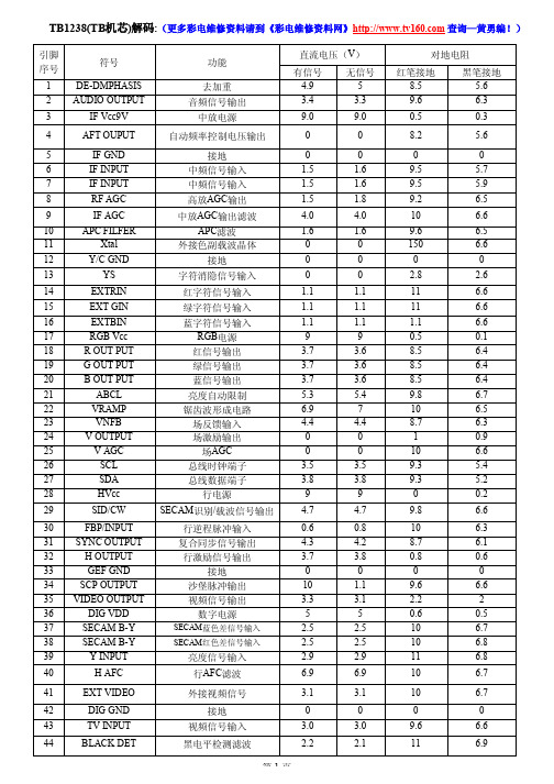
LA7833引脚功能
引脚
1 2 3 4 4 6 7
功能
接地端 场输出 自举升压电源端 场激励输入 负反馈输入及相位补偿 电源端 场逆程脉冲输出
直流电压
0V 13.6V 25.5V 0.8V 0.8V 26V 1.4V
纹波滤波电路引脚 第二伴音中频输出 调频直流反馈滤波电路引脚
电压
1.8V 0V 1.3V
+2.5V
+5V 2.45V 2.45V
1V 6.4V 0V 0V 2.3V 1.6V 0V +5V 3.6V 4.3V 0V 8V 8.8V 3.5V 5.6V 3.4V 3.5V
RXIK档对地电阻(黑表笔接地)
场AGC 总线时钟端子 总线数据端子
行电源 SECAM识别/载波信号输出
行逆程脉冲输入 复合同步信号输出 行激励信号输出
接地 沙堡脉冲输出 视频信号输出
数字电源
SECAM蓝色差信号输入 SECAM红色差信号输入
亮度信号输入 行AFC滤波
外接视频信号
接地 视频信Leabharlann 输入黑电平检测滤波直流电压(V)
有信号 4.9
800Ω 0
12.5K
12.8K
6K 13K 13K 13K 12.8K 13.2K
0 12.8K 13K 11.5K
1K 12.5K 12K
0 900Ω 600Ω 12.5K 12.2K 11.5K 12K
红笔接地 R×1K档
800Ω 0
19K
27K
5.5K 20K 20K 18K 28K 28K
华为CG9812 V500R005产品概述

华为CG9812产品概述(V500R005)华为技术有限公司2015年4月目录1 产品简介 (1)1.1 产品定位 (1)1.2 接口与协议 (2)2 产品特点 (4)2.1 先进的软硬件平台 (4)2.2 多接入性 (5)2.3 灵活的话单处理 (5)2.4 大容量和强大的处理性能 (5)2.5 可扩容性 (5)2.6 高可靠性 (6)2.7 方便实用的操作维护功能 (6)3 产品结构 (7)3.1 硬件结构 (7)3.1.1 机柜 (7)3.1.2 机框 (8)3.1.3 硬件组件设计标准 (10)3.2 软件结构 (11)4 业务与功能 (14)4.1 网元接口功能 (14)4.2 话单处理功能 (14)4.3 计费接口功能 (15)5 操作与维护 (16)5.1 话单浏览查询功能 (16)5.2 安全管理功能 (16)5.3 配置管理功能 (17)5.4 性能管理功能 (17)5.5 故障管理功能 (17)6 可靠性 (19)6.1 硬件可靠性 (19)6.2 软件可靠性 (20)6.3 话单可靠性 (21)7 技术指标 (23)7.1 性能指标 (23)7.2 对外接口规格指标 (23)7.3 可靠性指标 (24)7.4 功耗参数 (24)7.5 机柜参数 (25)7.6 环境指标 (25)7.7 EMC指标 (26)8 环境要求 (29)8.1 储存环境 (29)8.2 运输环境 (31)8.3 运行环境 (33)插图目录图1-1 CG典型组网 (2)图1-2 CG的接口与协议 (3)图3-1 N68E-22机柜 (8)图3-2 机框前视图 (9)图3-3 机框后视图 (10)图3-4 软件结构 (11)图3-5 AP进程 (12)表格目录表1-1 接口与协议 (3)表7-1 CG9812的性能指标 (23)表7-2 CG9812外部接口规格指标 (24)表7-3 可靠性指标 (24)表7-4 机柜物理参数 (25)表7-5 环境适应性 (25)表7-6 -48V电源端口传导发射指标 (26)表7-7 辐射发射指标要求 (26)表7-8 传导敏感度指标 (26)表7-9 辐射敏感度指标 (27)表7-10 静电放电指标 (27)表7-11 电子脉冲群指标 (27)表7-12 浪涌指标 (28)表8-1 气候环境要求 (29)表8-2 机械活性物质的浓度要求 (30)表8-3 化学活性物质的浓度要求 (30)表8-4 机械应力要求 (31)表8-5 气候环境要求 (31)表8-6 机械活性物质的浓度要求 (32)表8-7 化学活性物质的浓度要求 (32)表8-8 机械应力要求 (33)表8-9 气候环境要求 (34)表8-10 机械活性物质的浓度要求 (34)表8-11 化学活性物质的浓度要求 (34)表8-12 机械应力要求 (35)1 产品简介关于本章介绍CG的产品定位、接口与协议等。
长虹存储器
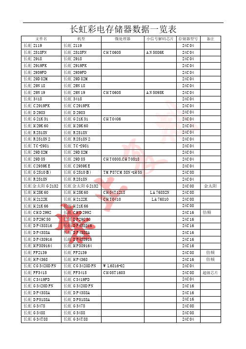
微处理器
CHT0605
CHT0605 CHT0406
CHT0808,CHT0818 TMP87CM38N-1H55 CH04T1218 CHT0410
WL6816-02 CH05T1603
小信号解码芯片
AN5086K AN5095K
LA76832N LA76810
存储器型号
24C04 24C04 24C04 24C04 24C04 24C04 24C04 24C04 24C04 24C04 24C04 24C04 24C04 24C04 24C04 24C04 24C04 24C04 24C04 24C08 24C04 24C08 24C08 24C08 24C08 24C16 24C16 24C16 24C16 24C16 24C16 24C08 24C16 24C04 24C08 24C04 24C16 24C16 24C16 24C08 24C08 24C04
TMP87CM38N-1H55
CHT0605 M37102M8-AB2SP 87CP38N-1P08
TB1238
AN5095 TA8759 TB1238
24C08 24C08 24C08 24C08 24C08 24C08 24C08 24C08 24C08 24C08 24C08 24C08 24C08 24C08 24C08 24C08 24C08 24C08 24C08 24C08 24C08 24C08 24C08 24C08 24C08 24C08 24C08 24C08 24C04 24C08 24C04 24C08 24C04 24C04 24C08 24C08 24C08 24C08 24C08 24C08 24C08 24C08 24C04 24C01 24C16
RT-121919中文资料

ECONOLINE - DC/DC-Converter
RT Series, 1 Watt, DIP14, Isolated Outputs (Dual Output) Features
● ● ● ● ●
Twin Independent Outputs Output/Output Isolation 1kVDC Power Sharing on Outputs Input/Output Isolation 1kVDC No Heatsink Required
9 10 11 14 NC = No Connection
10.00
7.62
7.10
2.0
15.24
3.05
Re2.54
1.00 ø+0.15/–0
XX.X ± 0.5 mm XX.XX ± 0.25 mm
14 PIN DIP Package
3rd angle projection
1
7
Bottom View
14 11 10 9 8
Pin Connections Pin # 1 7 8 Dual –Vin NC –Vout 2 +Vout 2 –Vout 1 +Vout 1 +Vin
19.90
RT-051212 RECOM ****
Output Power (Watts) 2.0 1.5 1.0 Safe Operating Area 0.5 0 -40 0 50 100 125 150 85 Operating Temperature ˚C
100mVp-p max. 70% min. 1.000VDC min. 10 GΩ min. 20pF min./94pF max. 1 Second 100kHz typ. –40°C to +85°C (see Graph) -55°C to +125°C 2.7g
MID 方案可选器件

(no SATA, over $20)
Rockchip RK2918 Coretex A8
(no SATA/CVBS)
Qualcom QSD8250 Coretex A8
TI Omap 36xx Coretex A8
(no SATA/CVBS)
Marvell Amarda610 Coretex A8
接近传感器
当你把手机靠近耳朵时,接近传感器会立刻把屏幕关起来来节省电源以及避 免误触屏幕。
Epson crystaห้องสมุดไป่ตู้ (PM: Derek.Wang)
MC-146 32.768K 12.5PF +-20PPM TG-5010LH 26M 04A FOR TD-
SCDMA
TG-5010LH 19.2M 06A FOR
Telechips TCC8803 MID Main Functions
Andriod2.2/2.3 WiFi: Atheros 6102/6302 3G: - Huawei 3G module:EM660C, EM660,
EM770/EM770W, MU509 - Huawei 3G dongle: -- EVDO: EC122, EC169C, -- WCDMA: E1750, E1752, K3765 - ZTE MF210 - Mobile Peak:3G module and dongle K80 DTV: CMMB, ISDB-T, DVB-T ATV: RDA GPS: SIRF A3, UBLOG Bluetooth: CSR(BC04/06/07), RDA
2.Wifi Chip Antenna: size: 5.2*3.7*0.7mm 2.0*1.2*0.55mm
- 1、下载文档前请自行甄别文档内容的完整性,平台不提供额外的编辑、内容补充、找答案等附加服务。
- 2、"仅部分预览"的文档,不可在线预览部分如存在完整性等问题,可反馈申请退款(可完整预览的文档不适用该条件!)。
- 3、如文档侵犯您的权益,请联系客服反馈,我们会尽快为您处理(人工客服工作时间:9:00-18:30)。
DS9818-05 March 2007
Features
z Internally Fixed Threshold 1.2V to 5V in 0.1V Step z High Accuracy ±1.5% z Low Supply Current 3μA z No External Components Required z Quick Reset within 20μs z Built-in Recovery Delay Include 0ms, 55ms, 220ms,
元器件交易网
RT9818
Micro-Power Voltage Detectors
General Description
The RT9818 is a micro-power voltage detector supervising the power supply voltage level for microprocessors (μP) or digital systems. It provides internally fixed threshold levels with 0.1V per step ranging from 1.2V to 5V, which covers most digital applications. It features low supply current of 3μA. The RT9818 performs supervisory function by sending out a reset signal whenever the VDD voltage falls below a preset threshold level. This reset signal will last the whole period before VDD recovering. Once VDD recovered upcrossing the threshold level, the reset signal will be released after a certain delay time. RT9818 is provided in SC-82, SC-70-3, SOT-23-3, SOT-23-5 and SOT-89 packages.
450ms Options z Low Functional Supply Voltage 0.9V z N-Channel Open-Drain Output z Small SC-82, SC-70-3, SOT-23-3, SOT-23-5, SOT-89
Packages z RoHS Compliant and 100% Lead (Pb)-Free
RT9818
Absolute Maximum Ratings (Note 1)
z Terminal Voltage (with Respect to GND)
VDD ------------------------------------------------------------------------------------------------------------------------ −0.3V to 6.0V z All Other Inputs -------------------------------------------------------------------------------------------------------- −0.3V to VDD+0.3V
`Suitable for use in SnPb or Pb-free soldering processes. `100%matte tin (Sn) plating.
1
元器件交易网
RT9818
Pin Configurations
GND
SOT-23-3 (L-Type)
NC
NC
5
4
123
RESET/ VDD GND RESET
SOT-23-5
1
2
3
RESET/ VDD GND RESET
SOT-89
Note : There is no pin1 indicator on top mark for SC-82 type, and pin 1 will be lower left pin when reading top mark from left to right. Pin2 of SC-82 is wider than other pins.
SC-70 / SC-82 ---------------------------------------------------------------------------------------------------------- 0.25W SOT-23-3 ---------------------------------------------------------------------------------------------------------------- 0.4W SOT-23-5 ---------------------------------------------------------------------------------------------------------------- 0.4W SOT-89 ------------------------------------------------------------------------------------------------------------------- 0.55W z Package Thermal Resistance (Note 4) SC-70 / SC-82, θJA ---------------------------------------------------------------------------------------------------- 400°C/W SOT-23-3, θJA ----------------------------------------------------------------------------------------------------------- 250°C/W SOT-23-5, θJA ----------------------------------------------------------------------------------------------------------- 250°C/W SOT-89, θJA ------------------------------------------------------------------------------------------------------------- 180°C/W z Lead Temperature (Soldering, 10sec.) ---------------------------------------------------------------------------- 260°C
Function Block DiagramVFra bibliotekDVSET
CMP
Timer
Threshold Voltage Setting
POR
Power On Reset
RESET/ RESET
N MOS
GND
2
DS9818-05 March 2007
元器件交易网
z Storage Temperature Range ---------------------------------------------------------------------------------------- −65°C to 125°C
z ESD Susceptibility (Note 2) HBM (Human Body Mode) ------------------------------------------------------------------------------------------ 2kV MM (Machine Mode) -------------------------------------------------------------------------------------------------- 200V
z Input Current, IVDD ----------------------------------------------------------------------------------------------------- 20mA z Power Dissipation, PD @ TA = 25°C
NC
4
3
1
2
RESET/ RESET
VDD
SC-82
RESET/
RESET
NC
4
3
1
2
VDD
GND
SC-82 (R-Type)
(TOP VIEW)
VDD
3
1
2
GND
RESET/ RESET
SC-70-3
VDD
3
1
2
RESET/ RESET
GND
SOT-23-3
VDD
3
1
2
GND
RESET/ RESET
Typical Application Circuit
VDD μP
RESET/ RESET