0.8V PLL
ttl工作电压

ttl工作电压ttl工作电压是指在TTL(晶体管-晶体管逻辑)电路中,所需的工作电压范围。
TTL是一种数字逻辑电路标准,广泛应用于计算机、通信和控制系统中。
TTL工作电压一般为5V,即电压范围在0V至5V之间。
这是因为TTL电路中使用的晶体管是NPN型的晶体管,其基极电压需要大于发射极电压才能使晶体管导通。
而在TTL电路中,逻辑1表示高电平,逻辑0表示低电平。
当输入电压大于2V时,被认为是逻辑1;当输入电压小于0.8V时,被认为是逻辑0。
TTL工作电压的范围是由TTL芯片内部的电路设计所决定的。
一般来说,TTL芯片内部会有上拉电阻和下拉电阻,用于确保输入电压在逻辑1和逻辑0之间的稳定性。
同时,TTL芯片还会有输入保护电路,用于防止外部电压超过额定范围,从而保护芯片不受损坏。
TTL工作电压的选择要根据具体的应用场景来确定。
一般来说,TTL 电路具有高速度和较低功耗的特点,适用于一些对速度要求较高的应用。
然而,TTL电路的电压范围较窄,对于一些需要更高电压范围的应用来说可能不合适。
在这种情况下,可以考虑使用CMOS (互补金属氧化物半导体)逻辑电路,其工作电压范围一般为3V 至15V。
在实际应用中,我们需要根据具体的电路设计要求来选择合适的TTL工作电压。
一般来说,TTL芯片的工作电压会在其规格书中进行明确说明。
同时,还需要考虑到外部电源的供电电压稳定性和噪声情况,以确保TTL电路的正常工作。
TTL工作电压是指TTL电路中所需的工作电压范围,一般为5V。
选择合适的工作电压可以保证TTL电路的正常工作和稳定性。
在实际应用中,需要根据具体的电路设计要求来确定工作电压,并考虑外部电源的供电电压稳定性和噪声情况。
这样才能确保TTL电路的可靠性和性能满足要求。
ICS501 LOCO PLL时钟乘法器数据表说明书
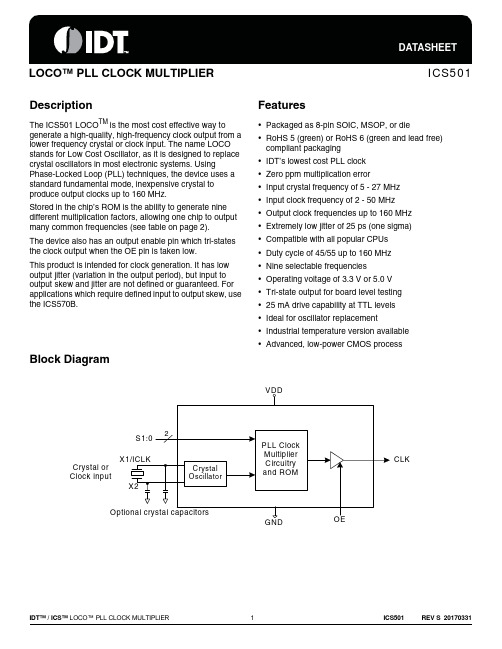
DescriptionThe ICS501 LOCO TM is the most cost effective way to generate a high-quality, high-frequency clock output from a lower frequency crystal or clock input. The name LOCO stands for Low Cost Oscillator, as it is designed to replace crystal oscillators in most electronic systems. Using Phase-Locked Loop (PLL) techniques, the device uses a standard fundamental mode, inexpensive crystal to produce output clocks up to 160 MHz.Stored in the chip’s ROM is the ability to generate nine different multiplication factors, allowing one chip to output many common frequencies (see table on page 2).The device also has an output enable pin which tri-states the clock output when the OE pin is taken low.This product is intended for clock generation. It has low output jitter (variation in the output period), but input to output skew and jitter are not defined or guaranteed. For applications which require defined input to output skew, use the ICS570B.Features•Packaged as 8-pin SOIC, MSOP, or die •RoHS 5 (green) or RoHS 6 (green and lead free) compliant packaging•IDT’s lowest cost PLL clock•Zero ppm multiplication error•Input crystal frequency of 5 - 27 MHz•Input clock frequency of 2 - 50 MHz•Output clock frequencies up to 160 MHz •Extremely low jitter of 25 ps (one sigma)•Compatible with all popular CPUs•Duty cycle of 45/55 up to 160 MHz•Nine selectable frequencies•Operating voltage of 3.3 V or 5.0 V•Tri-state output for board level testing•25 mA drive capability at TTL levels•Ideal for oscillator replacement•Industrial temperature version available •Advanced, low-power CMOS processBlock DiagramPin Assignment Clock Output Table0 = connect directly to ground 1 = connect directly to VDD M = leave unconnected (floating)Common Output Frequency Examples (MHz)Pin DescriptionsS1S0CLK Minimum Input 004X input per page 50M 5.3125X input 20 MHz 015X input per page 5M 0 6.25X input 4 MHz M M 2X input per page 5M 1 3.125X input 8 MHz 106X input per page 51M 3X input per page 5118X inputper page 5Output 2024303233.3337.54048506062.5Input1012101616.6612101216.661020Selection (S1, S0)M, M M, M 1, M M, M M, M M, 10, 00, 01, M 1, 0M, 1Output 6466.6672758083.3390100106.25120125Input1616.6612121016.661520201520Selection (S1, S0)0, 00, 01, 0M, 01, 10, 11, 00, 10, M1, 1M, 0PinNumberPin NamePin TypePin Description1XI/ICLK Input Crystal connection or clock input.2VDD Power Connect to +3.3 V or +5 V.3GND Power Connect to ground.4S1Tri-level IinputSelect 1 for output clock. Connect to GND or VDD or float.5CLK Output Clock output per table above.6S0Tri-level InputSelect 0 for output clock. Connect to GND or VDD or float.7OE Input Output enable. Tri-states CLK output when low. Internal pull-up.8X2OutputCrystal connection. Leave unconnected for clock input.External ComponentsDecoupling CapacitorAs with any high-performance mixed-signal IC, the ICS501 must be isolated from system power supply noise to perform optimally.A decoupling capacitor of 0.01µF must be connectedbetween VDD and the GND. It must be connected close to the ICS501 to minimize lead inductance. No external power supply filtering is required for the ICS501.Series Termination ResistorA 33Ω terminating resistor can be used next to the CLK pin for trace lengths over one inch.Crystal Load CapacitorsThe total on-chip capacitance is approximately 12 pF. A parallel resonant, fundamental mode crystal should be used. The device crystal connections should include pads for small capacitors from X1 to ground and from X2 to ground. These capacitors are used to adjust the stray capacitance of the board to match the nominally required crystal load capacitance. Because load capacitance can only be increased in this trimming process, it is important to keep stray capacitance to a minimum by using very short PCB traces (and no vias) between the crystal and device. Crystal capacitors, if needed, must be connected from each of the pins X1 and X2 to ground.The value (in pF) of these crystal caps should equal (C L -12 pF)*2. In this equation, C L = crystal load capacitance in pF. Example: For a crystal with a 16 pF load capacitance, each crystal capacitor would be 8 pF [(16-12) x 2 = 8].Absolute Maximum RatingsStresses above the ratings listed below can cause permanent damage to the ICS501. These ratings, which are standard values for IDT commercially rated parts, are stress ratings only. Functional operation of the device at these or any other conditions above those indicated in the operational sections of the specifications is not implied. Exposure to absolute maximum rating conditions for extended periods can affect product reliability. Electrical parameters are guaranteed only over the recommended operating temperature range.Recommended Operation ConditionsItemRatingSupply Voltage, VDD 7 VAll Inputs and Outputs-0.5 V to VDD+0.5 V Ambient Operating Temperature -40 to +85︒C Storage Temperature -65 to +150︒C Soldering Temperature260︒CParameterMin.Typ.Max.UnitsAmbient Operating Temperature (commercial)0+70︒C Ambient Operating Temperature (industrial)-4085︒C Power Supply Voltage (measured in respect to GND)+3.0+5.25VDC Electrical CharacteristicsVDD=5.0 V ±5%, Ambient temperature -40 to +85︒C, unless stated otherwiseParameter Symbol Conditions Min.Typ.Max.Units Operating Voltage VDD 3.0 5.25VInput High Voltage, ICLK only V IH ICLK (pin 1)(VDD/2)+1VInput Low Voltage, ICLK only V IL ICLK (pin 1)(VDD/2)-1VInput High Voltage V IH OE (pin 7) 2.0VInput Low Voltage V IL OE (pin 7)0.8VInput High Voltage V IH S0, S1VDD-0.5VInput Low Voltage V IL S0, S10.5VOutput High Voltage V OH I OH = -25 mA 2.4VOutput Low Voltage V OL I OL = 25 mA0.4VIDD Operating Supply Current, 20 No load, 100M20mA Short Circuit Current CLK output+70mA On-Chip Pull-up Resistor Pin 7270kΩInput Capacitance, S1, S0, and OE Pins 4, 6, 74pF Nominal Output Impedance20ΩAC Electrical CharacteristicsVDD = 5.0 V ±5%, Ambient Temperature -40 to +85︒ C, unless stated otherwiseNote 1: Measured with 15 pF load.Thermal Characteristics for 8SOICThermal Characteristics for 8MSOPParameterSymbolConditions Min.Typ.Max.UnitsInput Frequency, crystal input F IN 527MHz Input Frequency, clock inputF IN 250MHz Output Frequency, VDD = 4.75 to 5.25 V F OUT 0︒C to +70︒C 13160MHz -40︒C to +85︒C 13140 MHzOutput Frequency, VDD = 3.0 to 3.6 V F OUT 0︒C to +70︒C 13100MHz -40︒C to +85︒C 1390MHz Output Clock Rise Time t OR 0.8 to 2.0 V, Note 11ns Output Clock Fall Time t OF 2.0 to 8.0 V, Note 11nsOutput Clock Duty Cycle t OD1.5 V, up to 160 MHz4549-5155%PLL Bandwidth10kHzOutput Enable Time, OE high to outputon50ns Output Disable Time, OE low to tri-state 50ns Absolute Clock Period Jitter t ja Deviation from mean+70ps One Sigma Clock Period Jitter t js25psParameterSymbolConditionsMin.Typ.Max.UnitsThermal Resistance Junction to AmbientθJA Still air 150︒C/W θJA 1 m/s air flow 140︒C/W θJA 3 m/s air flow 120︒C/W Thermal Resistance Junction to Case θJC 40︒C/W Thermal Resistance Junction to Top of CaseψJTStill air20︒C/WParameterSymbolConditionsMin.Typ.Max.UnitsThermal Resistance Junction to AmbientθJA Still air95︒C/W Thermal Resistance Junction to CaseθJC48︒C/WPackage Outline and Package Dimensions (8-pin MSOP, 3.00 mm Body) Package dimensions are kept current with JEDEC Publication No. 95Package Outline and Package Dimensions (8-pin SOIC, 150 Mil. Narrow Body) Package dimensions are kept current with JEDEC Publication No. 95Ordering InformationPart / Order Number Marking Shipping Packaging Package Temperature 501MLF501MLF Tubes8-pin SOIC0 to +70︒ C501MLFT501MLF Tape and Reel8-pin SOIC0 to +70︒ C501MILF501MILF Tubes8-pin SOIC-40 to +85︒ C501MILFT501MILF Tape and Reel8-pin SOIC-40 to +85︒ C501GLF01GL Tubes8-pin MSOP0 to +70︒ C501GLFT01GL Tape and Reel8-pin MSOP0 to +70︒ C501GILF1GIL Tubes8-pin MSOP-40 to +85︒ C501GILFT1GIL Tape and Reel8-pin MSOP-40 to +85︒ C501-DWF-Die on uncut, probed wafers0 to +70︒ C501-DPK-Tested die in waffle pack0 to +70︒ C501E-DPK-Tested die in waffle pack0 to +70︒ C"LF" suffix to the part number are the Pb-Free configuration and are RoHS compliant.While the information presented herein has been checked for both accuracy and reliability, Integrated Device Technology (IDT) assumes no responsibility for either its use or for the infringement of any patents or other rights of third parties, which would result from its use. No other circuits, patents, or licenses are implied. This product is intended for use in normal commercial applications. Any other applications such as those requiring extended temperature range, high reliability, or other extraordinary environmental requirements are not recommended without additional processing by IDT. IDT reserves the right to change any circuitry or specifications without notice. IDT does not authorize or warrant any IDT product for use in life support devices or critical medical instruments.DISCLAIMER Integrated Device Technology, Inc. (IDT) and its affiliated companies (herein referred to as “IDT”) reserve the right to modify the products and/or specifications described herein at any time, without notice, at IDT’s sole discretion. Performance specifications and operating parameters of the described products are determined in an independent state and are not guaranteed to perform the same way when installed in customer products. The information contained herein is provided without representation or warranty of any kind, whether express or implied, including, but not limited to, the suitability of IDT's products for any particular purpose, an implied warranty of merchantability, or non-infringement of the intellectual property rights of others. This document is presented only as a guide and does not convey any license under intellectual property rights of IDT or any third parties.IDT's products are not intended for use in applications involving extreme environmental conditions or in life support systems or similar devices where the failure or malfunction of an IDT product can be reasonably expected to significantly affect the health or safety of users. Anyone using an IDT product in such a manner does so at their own risk, absent an express, written agreement by IDT.Corporate HeadquartersIntegrated Device Technology, For Sales800-345-7015408-284-8200Fax: 408-284-2775For Tech Support/go/supportInnovate with IDT and accelerate your future networks. Contact:。
TPS54560_数据手册
(1)有关导热的更多信息,请参阅 IC 封装导热应用报告 SPRA953。 (2)在特定环境温度 TA 下的额定功率有 150℃的结点温度来确定。这就导致失真大幅增加。请参见本数据表中功耗估 计的应用程序部分,获取更多信息。
电气特性
第 3 页 共 27 页
TPS54560
TJ = –40°C to 150°C, VIN = 4.5 to 60V (除非另有说明)
设备信息
引脚配置
第 1 页 共 27 页
TPS54560
HSOIC 封装 (顶部视图)
SLVSBN0 – MARCH 2013
引脚功能
引脚 NAME NO. BOOT VIN EN 1 2 3 I/O O I I 描述 BOOT 和 SW 之间应连接自举电容器。如果此电容上的电压小于高边 MOSFET 所需的最小值,输 出将被切断直到电容器被刷新。 输入电源电压为 4.5 V 至 60V。 使能引脚,内部存在上拉电流源。下拉低于 1.2 V 时禁用。浮动时使能。使用两个电阻调节输入欠 压锁定。参阅启用和调整欠压锁定的部分。
这个集成电路可以被静电损坏。德州仪器建议所有集成电路采取适当的预防措施。如果不遵守正 确的搬运和安装程序,可以造成损坏。 静电损害的范围可以从细微的性能下降到整个设备故障。精密集成电路可能更容易受到损害,因 为非常小的参数变化可能导致设备不能满足其公布的规格。 表 1 订购信息(1)
Tj 封装 部件编码 (2) –40°C to 150°C 8 脚 HSOIC TPS54560DDA (1)有关最新的封装和订货信息,请参阅本文档末尾的封装选项附录,或者登陆 TI 网站。 (2)DDA 包装是卷带式。R 可以后缀到设备类型(TPS54560 DDAR)。
精选ChinesePLLjitter资料

Data Input
Phase Detector
Phase Error Amplifier
Voltage Controlled Oscillator (VCO)
Recovered Clock
压控振荡器(VCO)可以跟踪信号抖动
Closed loop gain out A(s) G(s) G(s) e j(s) in 1 A(s)
Data Input
Phase Detector
Phase Error Amplifier
Voltage Controlled Oscillator (VCO)
Recovered Clock
鉴相器有效地提取输入信号中的抖动,调节压控振荡器(VCO)以跟踪输入抖 动
抖动跟踪是频率相关的
Closed loop gain out A(s) G(s) G(s) e j(s) in 1 A(s)
频谱线显示了周期抖动成分
1E-6
Jitter Spectrum
扩频时钟SSC和其谐波
100E-9
10E-9
Seconds (rms)
1E-9
100E-
1 MHz 周期抖动PJ (和
12
谐波)
10E-12
1E-12
100E15
10E-15
1E-15 1E+3
33 kHz
10E+3
100E+3
1 MHz
Data Input
Phase Detector
Phase Error Amplifier
Voltage Controlled Oscillator (VCO)
Recovered Clock
ttl电平电压

ttl电平电压TTL电平电压TTL(Transistor-Transistor Logic)电平电压是数字电路中常用的一种逻辑电平标准。
TTL电平指的是在数字电路中,逻辑0和逻辑1的表示电压范围。
在TTL电平标准中,逻辑0通常被定义为0V 至0.8V之间的电压,而逻辑1被定义为2.2V至5V之间的电压。
TTL电平电压的定义是为了确保数字电路的稳定性和可靠性。
在TTL电平标准中,逻辑0和逻辑1之间应有一个明确的电压差,以确保电路能够正确识别和处理信号。
在数字电路中,逻辑0表示低电平或关闭状态,而逻辑1表示高电平或开启状态。
TTL电平电压的使用在各种数字电路中非常广泛。
例如,在计算机系统中,TTL电平标准被用于处理器和内存之间的通信。
在通信领域,TTL电平电压被用于串行通信接口,如RS-232。
此外,TTL电平电压还被广泛应用于各种控制电路和传感器接口。
TTL电平电压的优点之一是其简单和易于实现。
TTL电路通常由晶体管和电阻器组成,成本低廉且易于制造。
此外,TTL电平标准具有较高的抗干扰能力和噪声容限,能够在较恶劣的环境条件下工作。
然而,TTL电平电压也存在一些缺点。
首先,TTL电路的功耗较高,因为晶体管在逻辑1和逻辑0之间切换时会产生较大的功耗。
其次,TTL电路的速度相对较低,无法满足一些高速应用的需求。
此外,TTL电平电压的传输距离有限,一般不超过几十米。
为了解决TTL电平电压的一些缺点,人们开发了许多其他的数字电平标准,如CMOS(Complementary Metal-Oxide-Semiconductor)和LVDS(Low Voltage Differential Signaling)。
这些新的电平标准具有更低的功耗、更高的速度和更远的传输距离。
TTL电平电压是一种常用的数字电路逻辑电平标准。
它的使用范围广泛,包括计算机系统、通信接口和控制电路等领域。
虽然TTL电平电压存在一些缺点,但它仍然是一种简单、可靠和易于实现的电平标准。
PLL502-01中文资料

FEATURES• Low phase noise VCXO output for the 24MHz to50MHz range (-130 dBc at 10kHz offset). • CMOS output.• 12 to 25MHz crystal input. • Integrated variable capacitors.• Selectable High Drive (36mA drive capability atTTL level) or Standard Drive (12mA drive capa-bility at TTL) output.• Wide pull range (+/- 250 ppm). • Low jitter (RMS): 10ps period. • 3.3V operation.• Available in 8-Pin TSSOP or SOIC.DESCRIPTIONSThe PLL502-01 is a low cost, high performance and low phase noise VCXO, providing less than -130dBc at 10kHz offset in the 24MHz to 50MHz operating range. The very low jitter (10 ps RMS period jitter) makes this chip ideal for applications requiring volt-age controlled frequency sources. Input crystal can range from 12 to 25MHz (fundamental resonant mode).PIN CONFIGURATIONOUTPUT RANGEMULTIPLIERFREQUENCY RANGEOUTPUT BUFFERx2 24 - 50MHz CMOSBLOCK DIAGRAMPLL502-0112345678XOUT N/C VIN GNDXIN VDD CLKOEPIN DESCRIPTIONSName Number Type DescriptionXOUT 1 I Crystal output pin.N/C 2 - Not connected.VIN 3 I Frequency control voltage input pin.GND 4 P Ground pin.CLK 5 O Output clock pin.VDD 6 P +3.3V VDD power supply pin.OE 7 I Output enable input pin. Disables (tri-state) output when low. Internal pull-up enables output by default if pin is not connected to low.XIN 8 I Crystal input pin.ELECTRICAL SPECIFICATIONS1. Absolute Maximum RatingsPARAMETERS SYMBOL MIN. MAX. UNITS Supply Voltage Range V CC-0.5 7 V Input Voltage Range V I-0.5 V CC+0.5 V Output Voltage Range V O-0.5 V CC+0.5 V Soldering Temperature 260 °C Storage Temperature T S-65 150 °C Ambient Operating Temperature* -40 85 °C Exposure of the device under conditions beyond the limits specified by Maximum Ratings for extended periods may cause permanent damage to the device and affect product reliability. These conditions represent a stress rating only, and functional operations of the device at these or any other conditions above the operational limits noted in this specification is not implied.* Note: Operating Temperature is guaranteed by design for all parts (COMMERCIAL and INDUSTRIAL), but tested for INDUSTRIAL grade only.2. AC Electrical SpecificationsPARAMETERS SYMBOL CONDITIONS MIN. TYP. MAX. UNITS Input Crystal Frequency 12 25 MHz0.8V ~ 2.0V with 10 pF load 1.15Output Clock Rise/Fall Time(Low Drive) 0.3V ~ 3.0V with 15 pF load 3.70.8V ~ 2.0V with 10 pF load 0.5Output Clock Rise/Fall Time(High Drive) 0.3V ~ 3.0V with 15 pF load 1.5nsOutput Clock Duty Cycle Measured @ 1.4V 45 50 55 % Short Circuit Current ±50 mA 3. Voltage Control Crystal OscillatorPARAMETERS SYMBOL CONDITIONS MIN. TYP. MAX. UNITS VCXO Stabilization Time * T VCXOSTB From power valid 10 msVCXO Tuning Range F XIN = 12 – 25MHz;XTAL C0/C1 < 250500 ppmCLK output pullability 0V ≤ VIN ≤ 3.3V ±250 ppm VCXO Tuning Characteristic 165 ppm/V Pull range linearity 10 % VCON pin input impedance 2000 kΩVCON modulation BW 0V ≤ VIN ≤ 3.3V, -3dB 25 kHz Note: Parameters denoted with an asterisk (*) represent nominal characterization data and are not production tested to any specific limits.4. Jitter and Phase Noise specificationPARAMETERS CONDITIONS MIN. TYP. MAX. UNITSRMS Period Jitter(1 sigma – 1000 samples) at 44MHz, with capacitivedecoupling between VDDand GND.10 psPhase Noise relative to carrier 44MHz @100Hz offset -80 dBc/Hz Phase Noise relative to carrier 44MHz @1kHz offset -110 dBc/Hz Phase Noise relative to carrier 44MHz @10kHz offset -130 dBc/Hz Phase Noise relative to carrier 44MHz @100kHz offset -123 dBc/Hz Phase Noise relative to carrier 44MHz @1MHz offset -124 dBc/Hz5. DC SpecificationPARAMETERS SYMBOL CONDITIONS MIN. TYP. MAX. UNITSSupply Current, Dynamic, with Loaded Outputs I DDF XIN = 12 - 25MHzOuput load of 10pF16 20 mAOperating Voltage V DD 3.13 3.47 V Output High Voltage V OH I OH = -12mA (low drive) 2.4 V Output Low Voltage V OL I LO = 12mA (low drive) 0.4 V Output High Voltage atCMOS levelV OHC I OH = -4mA (low drive) V DD – 0.4 V Output drive current At TTL level (High drive) 36 51 mAAt TTL level (Low drive) 12 17 mA Short Circuit Current ±50 mA VCXO Control Voltage VCON 0 3.3 V ESD Protection Human Body Model 30006. Crystal SpecificationsPARAMETERS SYMBOL MIN. TYP. MAX. UNITSCrystal Resonator Frequency F XIN12 25 MHzCrystal Loading Capacitance Rating C L (xtal)9.5 pFC0/C1 250 -ESR R S30 ΩNote: Crystal Loading rating: 9.5pF is the loading the crystal sees from the VCXO chip at VCON = 1.65V. It is assumed that the crystal will be at nominal frequency at this load. If the crystal requires more load to be at nominal frequency, the additional load must be added externally.This however may reduce the pull range.PACKAGE INFORMATIONEORDERING INFORMATIONFor part ordering, please contact our Sales Department:47745 Fremont Blvd., Fremont, CA 94538, USATel: (510) 492-0990 Fax: (510) 492-0991PART NUMBERThe order number for this device is a combination of the following:Device number, Package type and Operating temperature rangePLL502-01 X CPART NUMBERTEMPERATURATUREC=COMMERCIALM=MILITARYI=INDUSTRALPACKAGE TYPES=SOIC, O=TSSOPPhaseLink Corporation, reserves the right to make changes in its products or specifications, or both at any time without notice. The information fur-nished by Phaselink is believed to be accurate and reliable. However, PhaseLink makes no guarantee or warranty concerning the accuracy of said information and shall not be responsible for any loss or damage of whatever nature resulting from the use of, or reliance upon this product.LIFE SUPPORT POLICY: PhaseLink’s products are not authorized for use as critical components in life support devices or systems without the ex-press written approval of the President of PhaseLink Corporation.。
pll 电源设计要求
pll 电源设计要求
PLL(相位锁定环)电源设计要求主要包括以下几个方面:
1. 电源电压范围:PLL芯片的电源电压通常在到5V之间,因此要求电源的输出电压稳定在这个范围内。
2. 电源纹波:在设计电源时,需要评估电源的纹波,以保证电源纹波不影响PLL芯片的工作。
通常,电源的纹波要求低于50mV。
3. 供电方式:对于PLL电路,可能需要两种供电方式,分别为模拟部分和数字部分供电。
模拟部分供电要求对电源稳定性较高,不能有较大的纹波。
4. 供电电流:根据PLL电路的需求,需要提供适当的供电电流。
例如,PLL 模拟部分可能需要最大200mA的供电电流。
5. 电源滤波:为了提高电源质量,可以在电源设计中加入磁珠和电容组成的滤波电路。
6. 引脚连接:根据具体的PLL器件,PLL供电管脚的数量和标注可能不同。
例如,VCCAx引脚连接到的PLL模拟供电专用电源上,VCCD_PLLx连接到内核供电上。
以上是PLL电源设计的主要要求,具体要求可能会根据实际应用和PLL芯片的规格有所不同。
在设计时,需要仔细阅读PLL芯片的数据手册和技术规范,以确保电源设计的正确性和可靠性。
中文资料LTC3789

高效同步四开关升降压控制器LTC3789LTC3789系新研发出的高效率高性能升降压式开关稳压控制器,其输入电压可以从4V~38V,输出电压可以高于输入电压,可以低于输入电压为0.8V~38V,工作频率恒定,最高可达600KHz(200~600KHz)。
为电流模式工作。
输出电流反馈环提供对电池充电的支持,满足输入输出4V~38V的宽范围。
在工作区域有很低的噪声,LTC3789系目前最理想的可升降压的电池供电系统应用IC。
控制器工作模式由MODE/PLLIN端决定,MODE/PLLIN端可以在脉冲跳跃型和连续工作模式之间选择,它允许IC同步到外部时钟,脉冲跳跃型在轻载时提供十分低的纹波,与在连续工作模式时相同。
当输出电压进入设定值的10%以内时,PG端给出指标,LTC3789采用28PIN 的4mm×5mm的QFN封装。
LTC3789外部要求四只功率MOSFET,在V IN关断时V OUT即断开,软起动时间可调,主要用于自动化系统,大功率电池供电系统等。
* LTC3789基本应用电路图,如图1。
图1 LTC3789 的基本应用电路*LTC3789引脚功能说明如下:V FB(PIN1/PIN26)误差放大器反馈端,从输出端的电压分压器送到此端反馈电压。
SS(PIN2/PIN27)外部软起动输入端,LTC3789的V FB电压小于0.8V,内部一个3μA上拉电流源给外部C SS电容充电,其上斜电压时间为最终输出电压达到的时间。
SENSE+(PIN3/PIN28)将电流信号送到电流检测比较器;I TH 端电压由SENSE+与SENSE- 端之间的电压控制,外接电阻R SENSE设置限流阈值。
SENSE-(PIN4/PIN1)将电流信号送到电流检测比较器。
I TH(PIN5/PIN2)误差放大器输出和开关稳压器补偿点,增加此点电压到通道电流比较器触发点。
SGND(PIN6/PIN3)信号地。
必须与大电流地分开,并用C IN电容终止之。
- 1、下载文档前请自行甄别文档内容的完整性,平台不提供额外的编辑、内容补充、找答案等附加服务。
- 2、"仅部分预览"的文档,不可在线预览部分如存在完整性等问题,可反馈申请退款(可完整预览的文档不适用该条件!)。
- 3、如文档侵犯您的权益,请联系客服反馈,我们会尽快为您处理(人工客服工作时间:9:00-18:30)。
Vol.31,No.8Journal ofSemiconductors August 2010A 0.8V low power low phase-noise PLLHan Yan(韩雁)1,Liang Xiao(梁筱)1,Zhou Haifeng(周海峰)2; ,Xie Yinfang(谢银芳)3,and Wong Waisum(黄威森)4,(1Institute of Microelectronics and Photoelectronics,Zhejiang University,Hangzhou 310027,China)(2School of Information Science and Technology,Hangzhou Normal University,Hangzhou 310036,China)(3Department of Information Science and Electronic Engineering,Zhejiang University,Hangzhou 310027,China)(4Semiconductor Manufacturing International Corporation,Shanghai 201203,China)Abstract:A low power and low phase noise phase-locked loop (PLL)design for low voltage (0.8V)applications is presented.The voltage controlled oscillator (VCO)operates from a 0.5V voltage supply,while the other blocks operate from a 0.8V supply.A differential NMOS-only topology is adopted for the oscillator,a modified precharge topology is applied in the phase-frequency detector (PFD),and a new feedback structure is utilized in the charge pump (CP)for ultra-low voltage applications.The divider adopts the extended true single phase clock DFF in order to operate in the high frequency region and save circuit area and power.In addition,several novel design techniques,such as removing the tail current source,are demonstrated to cut down the phase noise.Implemented in the SMIC 0.13 m RF CMOS process and operated at 0.8V supply voltage,the PLL measures a phase noise of –112.4dBc/Hz at an offset frequency of 1MHz from the carrier and a frequency range of 3.166–3.383GHz.The improved PFD and the novel CP dissipate 0.39mW power from a 0.8V supply.The occupied chip area of the PFD and CP is 100 100 m 2.The chip occupies 0.63mm 2,and draws less than 6.54mW from a 0.8V supply.Key words:phase-locked loop;voltage control oscillator;low voltage;low power;low phase noise DOI:10.1088/1674-4926/31/8/085009EEACC:12301.IntroductionIntegrated circuit technology has maintained an exponen-tial scaling of the line-width of CMOS technologies deeper into nanoscale dimensions for the next two decades.This will in-crease the functionality density,the intrinsic speed of the de-vices and thus the signal processing capability of the circuits.However,in order to maintain the reliability,reduce the power density,and avoid breakdown as well as thermal problems,the maximum supply voltage has to be scaled down appropriately.All these features mentioned above have allowed the realiza-tion of systems with very high levels of integration on a mono-lithic silicon die at very low cost Œ1 .Compared with the reduc-tion of the supply voltage,the transistor’s threshold voltage is not reduced as aggressively.The low power supply voltages and the relatively large device threshold voltages are an obsta-cle for high performance analog circuit design.Recently,there have been several papers reporting that PLLs can operate at low-voltage supplies such as 0.65V Œ1 or 1V Œ2 .At supply voltages below 1V ,the design of analog circuits becomes very challenging since the traditional circuit techniques do not have sufficient voltage headroom.This is especially true for VCOs in wired and wireless communication systems for which high carrier power is necessary to lower the phase noise.In this paper,a low power,low phase noise PLL that op-erates from an aggressively downscaled supply voltage im-plemented in the 0.13 m RF CMOS process is presented.It demonstrates several design techniques overcoming the obsta-cles raised by voltage scaling and realizing low power dissi-pation.The detailed circuit design of the PLL is described,in-cluding the designs of the VCO,CP,PFD and divider.2.Architecture of the PLLA block diagram of the proposed PLL is depicted in Fig.1.The architecture of the system illustrated in Fig.1is simple and traditional.It comprises a PFD,CP,VCO,a dual-modulus prescaler,and an external third-order passive loop filter,which is designed for saving the core area.The detailed design tech-niques that are utilized for the low-voltage application of the PLL will be described in the following sections.3.Circuit design3.1.VCO designIn the PLL design,the most challenging task is to realize a high performance VCO with a reduced supply voltage and power consumption.While there are several VCO topologies,the complementary cross-coupled VCO topology is widely used due to its ability to suppress the 1/f noise.Unfortunately,Fig.1.Block diagram of the phase-locked loop.Corresponding author.Email:tianruo@Received 23November 2009,revised manuscript received 25February 2010c2010Chinese Institute of ElectronicsFig.2.Circuit diagram of the prototype VCO.this topology is not suitable for a low supply voltage because of the voltage headroom cut down by the CMOS and the current source.So a transformer-feedback VCO topology is usually adopted for low voltage applicationsŒ2 4 .But the drawback is that the topology and calculation are enormously complicated as it introduces mutual inductors.In this work,a differential NMOS-only topology is consid-ered to realize the ultra-low voltage supply application for a VCO as shown in Fig.2.As the NMOS-only VCO does not have PMOS cross-coupled pairs and current source,it reduces the voltage headroom,provides higher output swing for a low supply voltage and reduces the phase noise.From the mechanistic physical modelŒ5 mentioned,the noise factor F for the differential LC CMOS oscillator is given by:F D1C 4 RIV0C49g mbias R;(1)where I is the bias current, is the channel noise coefficient of the FET,and g mbias is the transconductance of the current source FET.Equation(1)indicates that the noise is derived from the tank resistance,the differential pair FETs,and the cur-rent source.In typical oscillators operating at high current lev-els,the current source contribution dominates other sources of phase noiseŒ5 .Adopting the proposed VCO,the current source is omitted,so the third term is removed from Eq.(1).Unfor-tunately,removing the tail current source has its drawbacks. That is,the impedance at the common-mode point S is reduced and the loaded factor when the oscillation forces M1and M2 into the triode region is loadedŒ6 .So two tail inductors are introduced in place of the tail current source raising the tail impedance at the oscillation frequency and its harmonics at the output node as well as lowering the voltage headroom.The control voltage V tune shown in Fig.2is connected to the output of the loop filter.If the output signal has high frequency harmonics,it will flow through the varactors to AC ground, degrading the Q factor and increasing the phase noise at the output.In order to suppress the high frequency signal but have no effect on DCvoltageŒ7 ,an inductor and varactors inseriesFig.3.Schematic of precharge type PFD.Fig.4.Output of the PFD.(a)f in D1:11GHz.(b)f in D1:25GHz.with passive metal–isolator–metal capacitors are used to makea clean control voltage.Flicker noise in M1,M2is modeled as a fluctuating off-set voltage that unbalances the differential pair.After com-mutation,the fluctuation modulates the oscillation frequencyand ultimately results in output phase noise.By eliminatingthe common mode capacitance,the flicker noise conversion isnulledŒ8 .The capacitor C s is sized to appear as low impedancefor the fundamental tone that circulates differentially in thecross coupled pair and very high impedance to flicker noise inthe switching pair.With proper choice of the capacitance value,the fundamental oscillation is hardly disturbed and flickernoise is prevented from modulating the oscillation frequency.3.2.PFD and CPThe PFD is implemented by modified prechargeŒ9 topol-ogy since it can operate from a0.8V supply(Fig.3).The mod-ified precharge PFD(MPTPFD)has better speed performancethan a conventional PFD.However,till now,all the papers con-cerning it said that it had a dead zone around zero phase error.Through careful analysis of the construct of the pt-PFD,it isfound that the dead zone can be removed by suitably designingFig.5.Proposed charge pump topology.Fig.6.Charge pump current matching characteristic under different process corners.Fig.7.Schematic of the divide-by 128/129dual-modulus prescaler.the size of the transistors.The maximum operation frequency is defined as the shortest period with the correct UP and DN sig-nals together with the inputs having the same frequency plus 90ıphase difference Œ10 .Using this comparison criterion,the operation frequency for the proposed PFD is obtained greater than 1.11GHz.The simulation result is shown in Fig.4.The proposed charge pump is shown in Fig.5.In the 0.13 m 1P8M CMOS process,the thresholdvoltage for NMOS and PMOS is about0.3V ,which leads the output voltage rangefor a conventional charge pump to be reduced as low as 0.2V .Fig.8.Simulation results of the prescaler.Fig.9.Die micrograph of the proposed PLL.Fig.10.Tuning characteristics of the proposed VCO.So with the reduced supply voltage,traditional stacking tran-sistor stages should be prevented.Thus,the switches at the gate terminals of M2and M3are utilized to control the functionality of charging or discharging the loop filter.It is also noted that when the controlled voltage approaches the supply voltage or the ground potential,the mismatch between the up and down currents becomes large enough to greatly degrade the perfor-mance of the PLL.So the controlled voltage is connected to the gate terminals of M5and M6establishing a negative feedback to suppress the mismatch over a large voltage range Œ11 .Fig-ure 6shows the simulated systematic mismatch between theFig.11.Frequency spectrum of the output signal from the PLL.(a)f in D 26:35MHz,f out D 3:3728GHz.(b)f in D 26:40MHz,f out D 3:3793GHz.(c)f in D 26:43MHz,f out D 3:3830GHz.(d)f in D 26:48MHz,f out D 3:3895GHz.up and down currents as a function of the output voltage for the proposed charge pump.3.3.Divider designA divide-by 128/129dual-modulus prescaler circuitry us-ing the traditional transmission gate flip-flop (TGFF)is shown in Fig.7.Note that the speed of the divider is limited by a divide-by 4/5prescaler circuit,so the extended true-single-phase-clock CMOS circuit technique (E-TSPC)Œ12 is intro-duced,which enhances the technique for high-speed opera-tions.Based on 0.13 m CMOS technology with a supply voltage of 0.8V ,the prescaler circuit in the gray area of Fig.7can run at 4GHz with 0.71mW power consumption.The asynchronous divide-by N ,where N is 32in this divide-by 128/129prescaler,consists of one true-single-phase-clock (TSPC)FF Œ13 .It is simple and can work well at high frequen-cies.4.Experimental resultsThe circuit was fabricated in a standard 0.13 m CMOS process.The die photo is shown in Fig.9,and its area is 1:2 1:1mm 2,including the pads,while the loop filter is realized by off-chip components.Each building block is encircled by double guardrings to minimize substrate noise interference.Empty ar-eas are filled with poly and metal layers to meet the requirement for the minimum density of these layers.Open-drain NMOSbuffers are used for VCO output measurement Œ14 .Fig.12.Phase noise for the VCO and PLL at 1MHz offset frequency.By a combining discrete and continuous tuning Œ15 ,a fam-ily of overlapping tuning curves which guarantee continuous frequency coverage over the tuning range are measured and shown in Fig.10.This VCO is tunable over 220MHz with a sensitivity of about 30MHz/V .In Fig.11the frequency spec-trum of the output signal from the PLL with different reference frequencies is shown,while Figure 12shows the phase noise of the VCO and PLL at 1MHz offset along the whole frequency tuning range.It also shows that the phase noise displays lit-tle dependence on the frequency tuning.For example,in the whole frequency tuning range,the output phase noise reaches its worst value of –112.45dBc/Hz at 1MHz offset 3.2877GHz,parison of PLL performance.Reference V DD(V)CMOSprocess( m)Frequency(GHz)Phase noise@1MHz(dBc/Hz)Settlingtime( s)Power(mW)Divider FOMRef.[1]0.650.09 2.4–2.6–113–6Integer-N–173.5 Ref.[2]10.18 4.112–4.352–114869.68Integer-N–176.6 Ref.[3]0.80.18 1.06–1.4–121200 4.92Fractional-N–176.4 Ref.[16] 1.10.18 5.06–6.08–1144031Integer-N–173.9 Ref.[17] 1.20.13 2.4–2.48–1257015Fractional-N–180.8 This work0.80.13 3.17–3.38–112.437.2 6.542Integer-N–174.8Fig.13.Measured acquisition of the voltage controlled signal. which results in the worst FOM of–174.630dBc,while the out-put phase noise reaches the best value of–114.95dBc/Hz at1 MHz offset3.3895GHz,and the optimum FOM is–177.396 dBc.Figure13shows the control voltage signal of the VCO, it also shows that the settling time of the proposed PLL is less than50 s.The total power consumption of this PLL chip was measured to be6.542mW,and the power consumption for the VCO is1.3mW.The performance of the proposed PLL is sum-marized in Table1,compared with the performance of recently published PLLs with low supply voltages in the CMOS pro-cess.In order to compare the proposed PLL performance to other published work,it is useful to employ a FOM that cap-tures three important performance parameters for oscillators: frequency,phase noise and power consumption.5.ConclusionsIn this paper,a low phase noise,low power PLL is pre-sented.The circuit is implemented in a standard0.13 m CMOS process.With the improved PFD and novel CP struc-ture,their dissipation is cut down to0.39mW from a0.8V supply.In addition,a differential NMOS-only topology that re-moves the tail current source is adopted for the VCO to ensure ultra-low voltage operation and reduce the phase noise.With a0.8V supply,the PLL measures a phase noise of–114.95 dBc/Hz at an offset of1MHz with a center frequency of3.3895 GHz and a frequency tuning range from3.17to3.38GHz.The proposed PLL occupies a chip area of1.32mm2and dissipates only6.54mW.AcknowledgementThe author would like to thank Semiconductor Manufac-turing International Corporation(SMIC)for chip fabrication and technical support.References[1]Yu S A,Kinget P.A0.65-V2.5-GHz fractional-N synthesizerwith two-point2-Mb/s GFSK data modulation.IEEE J Solid-State Circuits,2009,44(9):2411[2]Leung L L K,Luong H C.A1-V,9.7-mW CMOS frequency syn-thesizer for IEEE802.11a transceivers.IEEE Trans Microw The-ory Tech,2008,56(1):39[3]Wang W,Luong H C.A0.8-V4.9-mW CMOS fractional-Nfrequency synthesizer for RFID application.Solid-State Circuits Conference,2006:146[4]Kwok K,Luong H C.Ultra-low-voltage high-performanceCMOS VCOs using transformer feedback.IEEE J Solid-State Circuits,2005,40:652[5]Rael J J,Abidi A A.Physical processes of phase noise in differ-ential LC oscillators.Proc IEEE Custom Integrated Circuits Con-ference,2000:569[6]Hegazi E,Sjoland H,Abidi A A.A filtering technique to lower LCoscillator phase noise.IEEE J Solid-State Circuits,2001,36(12): 1921[7]Zhou H F,Han Y,Dong S R,et al.An ultra-low-voltage high-performance VCO in0.13 m CMOS.Journal of Electromagnetic Waves and Applications,2008,22(17/18):2417[8]Ismail A,Abidi A A.CMOS differential LC oscillator with sup-pressed up converted flicker noise.Proc Int Solid-Stage Circuits Conference,ISSCC,San Francisco,USA,2003:98[9]Lee G B,Chan P K,Siek L.A CMOS phase frequency detectorfor charge pump phase-locked loop.42nd Midwest Symposium on Circuits and Systems,1999,2:601[10]Razavi B.Monolithic phase-locked loops and clock recovery cir-cuits:theory and design.Wiley-IEEE Press,1996[11]Hsieh H H,Lu C T,Lu L H.A0.5-V1.9-GHz low-power phase-locked loop in0.18- m CMOS.20th Symposium on VLSI Cir-cuits,Kyoto,Japan,Jun2007:164[12]Navarro J,Noije W V.A1.6-GHz dual modulus prescaler usingthe extended true-single-phase-clock CMOS circuit technique(E-TSPC).IEEE J Solid-State Circuits,1999,34:97[13]Yuan J,Svensson C.High-speed CMOS circuit technique.IEEEJ Solid-State Circuits,1989,24:62[14]Andreani P,Mattisson S.On the use of MOS varactors in RFVCO’s.IEEE J Solid-State Circuits,2000,35:905[15]Hegazi E,Abidi A A.A17-mW transmitter and frequency syn-thesizer for900MHz GSM fully integrated in0.35- m CMOS.IEEE J Solid-State Circuits,2003,38(5):782[16]Cheng J L,Wang C S,Li W C,et al.A1.1-V CMOS frequencysynthesizer with pass-transistor-logic prescaler for U-NII band system.IEEE International Symposium on VLSI Design,Au-tomation and Test,2008:117[17]Marletta M,Aliberti P,Pulvirenti M,et al.Fully integrated frac-tional PLL for Bluetooth application.IEEE Radio Frequency In-tegrated Circuits(RFIC)Symp Dig Papers,2005:557。