2SC2075中文资料
2SC2734中文资料
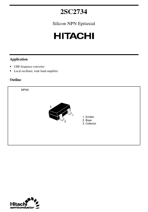
2SC2734Silicon NPN EpitaxialApplication• UHF frequency converter• Local oscillator, wide band amplifierOutline2SC27342Absolute Maximum Ratings (Ta = 25°C)ItemSymbol Ratings Unit Collector to base voltage V CBO 20V Collector to emitter voltage V CEO 11V Emitter to base voltage V EBO 3V Collector currentI C 50mA Collector power dissipation P C 150mW Junction temperature Tj 150°C Storage temperatureTstg–55 to +150°CElectrical Characteristics (Ta = 25°C)ItemSymbol Min Typ Max Unit Test conditions Collector to base breakdown voltageV (BR)CBO20——V I C = 10 µA, I E = 0Collector to emitter breakdown voltageV (BR)CEO 11——V I C = 1 mA, R BE = ∞Emitter to base breakdown voltageV (BR)EBO 3——V I E = 10 µA, I C = 0Collector cutoff current I CBO ——0.5µA V CB = 10 V, I E = 0Collector to emitter saturation voltageV CE(sat)——0.7VI C = 10 mA, I B = 5 mA DC current transfer ratio h FE 2090200V CE = 10 V, I C = 5 mA Gain bandwidth product f T 1.4 3.5—GHz V CE = 10 V, I C = 10 mA Collector output capacitance Cob —0.9 1.5pF V CB = 10 V, I E = 0, f = 1 MHz Conversion gainCG—15—dB V CC = 6 V, I C = 2 mA,f = 900 MHz,f OSC = 930 MHz (0dBm),f out = 30 MHzNoise figure NF —9—dBV CC = 6 V, I C = 2 mA,f = 900 MHz,f OSC = 930 MHz (0dBm),f out = 30 MHz Oscillating output voltage V OSC—140—mVV CC = 6 V, I C = 5 mA,f = 930 MHzNote:Marking is “GC”.2SC273432SC273442SC273452SC273462SC273472SC27348Hitachi CodeJEDECEIAJWeight (reference value)MPAK—Conforms0.011 gUnit: mm元器件交易网Cautions1.Hitachi neither warrants nor grants licenses of any rights of Hitachi’s or any third party’s patent,copyright, trademark, or other intellectual property rights for information contained in this document.Hitachi bears no responsibility for problems that may arise with third party’s rights, includingintellectual property rights, in connection with use of the information contained in this document.2.Products and product specifications may be subject to change without notice. Confirm that you have received the latest product standards or specifications before final design, purchase or use.3.Hitachi makes every attempt to ensure that its products are of high quality and reliability. However,contact Hitachi’s sales office before using the product in an application that demands especially high quality and reliability or where its failure or malfunction may directly threaten human life or cause risk of bodily injury, such as aerospace, aeronautics, nuclear power, combustion control, transportation,traffic, safety equipment or medical equipment for life support.4.Design your application so that the product is used within the ranges guaranteed by Hitachi particularly for maximum rating, operating supply voltage range, heat radiation characteristics, installationconditions and other characteristics. Hitachi bears no responsibility for failure or damage when used beyond the guaranteed ranges. Even within the guaranteed ranges, consider normally foreseeable failure rates or failure modes in semiconductor devices and employ systemic measures such as fail-safes, so that the equipment incorporating Hitachi product does not cause bodily injury, fire or other consequential damage due to operation of the Hitachi product.5.This product is not designed to be radiation resistant.6.No one is permitted to reproduce or duplicate, in any form, the whole or part of this document without written approval from Hitachi.7.Contact Hitachi’s sales office for any questions regarding this document or Hitachi semiconductor products.Hitachi, Ltd.Semiconductor & Integrated Circuits.Nippon Bldg., 2-6-2, Ohte-machi, Chiyoda-ku, Tokyo 100-0004, Japan Tel: Tokyo (03) 3270-2111 Fax: (03) 3270-5109Copyright ' Hitachi, Ltd., 1999. All rights reserved. Printed in Japan.Hitachi Asia Pte. Ltd.16 Collyer Quay #20-00Hitachi TowerSingapore 049318Tel: 535-2100Fax: 535-1533URLNorthAmerica : http:/Europe : /hel/ecg Asia (Singapore): .sg/grp3/sicd/index.htm Asia (Taiwan): /E/Product/SICD_Frame.htm Asia (HongKong): /eng/bo/grp3/index.htm Japan : http://www.hitachi.co.jp/Sicd/indx.htmHitachi Asia Ltd.Taipei Branch Office3F, Hung Kuo Building. No.167, Tun-Hwa North Road, Taipei (105)Tel: <886> (2) 2718-3666Fax: <886> (2) 2718-8180Hitachi Asia (Hong Kong) Ltd.Group III (Electronic Components)7/F., North Tower, World Finance Centre,Harbour City, Canton Road, Tsim Sha Tsui,Kowloon, Hong Kong Tel: <852> (2) 735 9218Fax: <852> (2) 730 0281 Telex: 40815 HITEC HXHitachi Europe Ltd.Electronic Components Group.Whitebrook ParkLower Cookham Road MaidenheadBerkshire SL6 8YA, United Kingdom Tel: <44> (1628) 585000Fax: <44> (1628) 778322Hitachi Europe GmbHElectronic components Group Dornacher Stra§e 3D-85622 Feldkirchen, Munich GermanyTel: <49> (89) 9 9180-0Fax: <49> (89) 9 29 30 00Hitachi Semiconductor (America) Inc.179 East Tasman Drive,San Jose,CA 95134 Tel: <1> (408) 433-1990Fax: <1>(408) 433-0223For further information write to:。
2SA系列(PNP型)三极管全参数表

-1.5
-180
-160
120M
60-200
3CA10F
2SA1011S
SANYO
硅PNP三极管,功率放大,场输出,配对管2SC2344
25
-1.5
-180
-160
120M
60-200
3CA10F
2SA1011W
WS
硅PNP三极管,功率放大,场输出,配对管2SC2344
25
-1.5
-180
-160
200m
-500m
-40
-32
200M
82-390
2SA1037AK
ROHM
硅PNP三极管,一般小信号放大,配对管2SC2412K
200m
-150m
-60
-50
140M
120-560
2SA1037B
LRC
硅PNP三极管,一般小信号放大,配对管2SC2412K/2SC4081
200m
-150m
-60
-50
-25
200M
50-340
CK77A
2SA0684
PANASONIC
硅PNP三极管,低频功率放大和驱动,配对管2SC1384
1
-1.5
-60
-50
200M
50-340
CK77A
2SA0794
PANASONIC
硅PNP三极管,低频功率放大和驱动,配对管2SC1567
1.2
-500m
-100
-100
120M
60M
70-240
3CA10D
2SA1013
长电
硅PNP三极管,TO-92,放大
2SC1846中文资料

2SC3545中文资料

1.6
1.4
1.2
1.0
0.9
0.8
0.5
REACTANCE COMPONENT
( ) ––R–– ZO
0.2
S11e
0.4
0.6
0.8
0.2 GHz
1.0
0.8 1.0
IC = 5 mA IC = 10 mA
1.8 2.0
3.0
4.0
5.0
10 20 50
0.2 GHz
S22e 1.6 GHz
10 20
2
CC.rb'b-Collector to Base Time Constant-ps
Gmax-Maximum Available Gain-dB |S21e|2-Insertion Gain-dB
Cre-Feed-back Capacitance-pF
2SC3545
TYPICAL DEVICE CAPACITANCE vs. COLLECTOR TO BASE VOLTAGE 3
元器件交易网
S-PARAMETER
S11e, S22e-FREQUENCY CONDITION VCE = 10 V, 200 MHz Step
0.6 0.8
0.7
0.404.06 0.5
0.09
0.007.413300.008.42
0.6
0.41 120
0.7
0.10 0.40
S21
114.1 92.9 81.7 70.2 62.8 54.4 47.9 40.9
S21
104.9 87.4 78.0 67.2 60.1 52.5 46.3 39.5
S12
0.037 0.055 0.077 0.098 0.108 0.125 0.148 0.160
三极管2SC
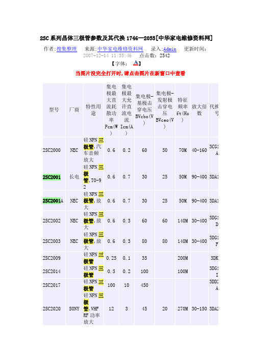
2SC系列晶体三极管参数及其代换1746--2055[中华家电维修资料网]作者:搜集整理来源:中华家电维修资料网录入:Admin更新时间:2007-12-1411:55:46点击数:2542【字体:】当图片没完全打开时,请点击图片在新窗口中查看型号厂商特性用途集电极最大直流耗散功率Pcm(W)集电极最大允许直流电流Icm(A)集电极-基极击穿电压BVcbo(V)集电极-发射极击穿电压BVceo(V)特征频率ft(Hz)放大倍数代换型号2SC2000 NEC 硅NPN三极管,汽车音频放大0.6 0.2 60 50 70M 40-1603CG180A2SC2001长电硅NPN三极管,TO-920.6 0.7 30 25 50M 90-400 3DA18A2SC2001A NEC 硅NPN三极管,放大0.6 0.7 30 25 50M 90-400 3DA18A2SC2002 NEC 硅NPN三极管,放大0.6 0.3 60 60 140M 30-4003DG130D2SC2003 NEC 硅NPN三极管,放大0.6 0.3 80 80 140M 30-4003DG182F2SC2009 硅NPN三极管0.25 0.1 35 200M 3DK2A2SC2014 硅NPN三极管0.5 0.2 100 100M3DG180I2SC2017 硅NPN三极管100 10 4503DD264A2SC2020 SONY 硅NPN三极管,VHFRF功率放大12 3 45 20 270M 30-150 3DA22A2SC2021ROHM极管,一般小信号放大,配对管2SA937 0.3 0.1 50 40 180M120-8202SC2021L N 硅NPN 三极管,低噪声 0.3 0.15 50 180-5602SC2022硅NPN 三极管 30130010M3DK205F 2SC2023SANKEN 硅NPN 三极管,串联调整,开关,一般放大 40 2 300 300 10M 303DK206F2SC2024硅NPN 三极管 1 1 80 150M 3DK30C2SC2025NEC硅NPN 中功率UHF-VHF 三极管 0.25 0.07 25 12 4.5G 20-2502SC2026NEC 硅NPN 三极管,VHF ,UHF 低噪声放大 0.25 0.05 30 14 2G 25-200 3DG44C2SC2027硅NPN 三极管 50 5 1500 3DA58I2SC2028 FUJI 硅NPN 三极管,高频放大 5 1.5 80 50 250M 90-320 3DA14B 2SC2029硅NPN 三极管 10280 150M 3DK104E 2SC203硅NPN 三极管 0.35 0.2 40 350M3DG130C2SC2034 TOSHIBA硅NPN 三极管,功率放大 12 2 120 90 150M 50-200 2SC2035硅NPN 三极管0.3 0.3 50 350M 3DK29B2SC2036TOSHIB A 资料来自网上118080150M100整理,硅NPN,功率放大2SC2037 NEC 一般NPN晶体管0.25 0.07 25 12 4.5G 20-2502SC2039 硅NPN三极管80 8 70 200M 3DA73B2SC204 硅NPN三极管0.35 0.2 20 350M3DG130C2SC2043 FUJI 硅NPN三极管,功率放大25 8 70 70 220M 20-2002SC2050 FUJI 硅NPN三极管,功率放大13 8 70 70 150M 20-1502SC2053 MIT 硅NPN三极管,VHFRF放大0.6 0.3 40 17 10-1802SC2055 MIT 硅NPN三极管,VHFRF放大0.5 0.3 18 9 1.7G 10-1803DG130A。
2SC2925S资料

Unit: mm
4.0±0.2
M Di ain sc te on na tin nc ue e/ d
0.7±0.1
• High forward current transfer ratio hFE • Low collector-emitter saturation voltage VCE(sat)
750
mW
or m
1 000 0.15 11
0.7
A
2.3±0.2
IC = 10 µA, IE = 0 IC = 1 mA, IB = 0 IE = 10 µA, IC = 0
Collector-emitter voltage (Base open) Emitter-base voltage (Collector open)
50
15
Collector-base cutoff current (Emitter open)
*
VCB = 20 V, IE = 0 VCE = 20 V, IB = 0
si
Collector-emitter cutoff current (Base open) Forward current transfer ratio
Unit V V V µA µA V pF
Publication date: March 2003
SJC00124BED
1
This product complies with the RoHS Directive (EU 2002/95/EC).
2SC2925
PC Ta
1.0
120 Ta = 25°C
This product complies with the RoHS Directive (EU 2002/95/EC).
2SK2645中文资料(fuji)中文数据手册「EasyDatasheet - 矽搜」

FAP-IIS系列
特征
高速开关 低导通电阻 无二次击穿 低驱动电源 高压 V GS =±30V防护证 额定重复性雪崩
2SK2645-01MR
外形图
N沟道MOS-FET
600V
1,2
9A
50W
应用
开关稳压器
UPS DC-DC转换
通用功率放大器
最大额定值和特性
- 绝对最大额定值 (
10
[A] Eas [mJ] I
12
Starting T [°C]
V [V] 本规范如有变更,恕不另行通知!
t [s]
雪崩能力 二极管正向导通电压 反向恢复时间 反向恢复电荷
V GS =0V V DS= V GS Tch=25°C Tch=125°C V DS=0V V GS =10V V DS=25V V DS=25V V GS =0V f=1MHz V CC=300V ID=9A V GS=10V RGS =10 L = 100µH Tch=25°C I F=2xI DR V GS=0V T ch=25°C IF=I DR V GS=0V -dI F/dt=100A/µs T ch=25°C
Unit V A A V A mJ W °C °C
- 电气特性(T
Item
漏源击穿电压 门门限电压 零栅压漏电流 门源漏电流 漏源极导通状态电阻 正向跨 输入电容 输出电容 反向传输电容 导通时间t on (t on =t d(on) +t r ) 关断时间t
off (ton=t d(off)+t f)
Typical Forward Transconductance vs. I
Gate Threshold Voltage vs. T
2SC2735中文资料

Collector to emitter breakdown V(BR)CEO 20 voltage
Emitter to base breakdown voltage
V(BR)EBO
3
Collector cutoff current
I CBO
—
Collector to emitter saturation VCE(sat)
2.2 k
VBB 1,000 p
Vosc Output 1.5 p
1.1 M
7p
12 p
4,700 p
L1
200
4,700 p 1SV70
200 µ D.U.T.
20,000 p 5.6 p
VCC 4,700 p
VT
fosc Monitor
Unit C : F R:Ω L:H
L1 : Inside dia φ3 mm, φ3 mm Enameled Copper Wire 12 Turns Test Frequency : fosc = 300 MHz
Symbol VCBO VCEO VEBO IC PC Tj Tstg
Ratings
Unit
30
V
20
V
3
V
50
mA
150
mW
150
°C
–55 to +150
°C
Electrical Characteristics (Ta = 25°C)
Item
Symbol Min
Collector to base breakdown V(BR)CBO 30 voltage
8
元器件交易网
3
–