OV6620中文资料OV7620中文资料
(en)OV7620
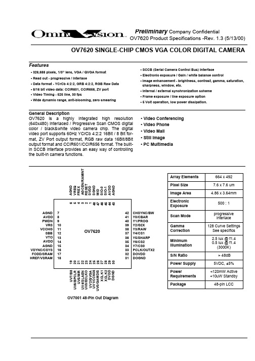
OV7620 Product Specifications -Rev. 1.3 (5/13/00)OV7620 SINGLE-CHIP CMOS VGA COLOR DIGITAL CAMERAFeatures• 326,688 pixels, 1/3” lens, VGA / QVGA format • Read out - progressive / Interlace• Data format - YCrCb 4:2:2, GRB 4:2:2, RGB Raw Data • 8/16 bit video data: CCIR601, CCIR656, ZV port • Video Timing - 525 line, 30 fps• Wide dynamic range, anti-blooming, zero smearing• SCCB (Serial Camera Control Bus) interface • Electronic exposure / Gain / white balance control• Image enhancement - brightness, contrast, gamma, saturation, sharpness, window, etc.• Internal / external synchronization scheme • Frame exposure / line exposure option • 5 Volt operation, low power dissipation.General DescriptionOV7620 is a highly integrated high resolution (640x480) Interlaced / Progressive Scan CMOS digital color / black&white video camera chip. The digital video port supports 60Hz YCrCb 4:2:2 16Bit / 8 Bit for-mat, ZV Port output format, RGB raw data 16Bit/8Bit output format and CCIR601/CCIR656 format. The built-in SCCB interface provides an easy way of controlling the built-in camera functions.• Video Conferencing • Video Phone • Video Mail • Still Image • PC MultimediaOV7001 48-Pin Out DiagramU V 7/B 8U V 6/B P C L R U V 5/M I R U V 4/S L A E N U V 3/E C L K O U V 2/Q V G A U V 1/C C 656U V 0/G A M D I S X C L K 1X C L K 2D V D D D G N D 654321484746454443A G N D V R E Q F R E X A G C E N /R A M I N T R E S E T S V D D S G N D MI D S I O -0S I O -1A V D D A G N D789101112131415161718AGND AVDD PWDN VRS VCCHGSBB VTO AVDD AGNDVSYNC/CSYS FODD/SRAM HREF/VSRAM 313233343536373839404142DOGNDDOVDD PCLK/OUTX2Y7/CS0Y6/CS2Y5/SHARP Y4/CS1Y3/RAW Y2/G2X Y1/PROG Y0/CBAR CHSYNC/BW 192021222324252627282930OV7620Array Elements 664 x 492Pixel Size 7.6 x 7.6 um Image Area 4.86 x 3.64mmElectronic Exposure500 : 1Scan Mode progressive interlace Gamma Correction 128 Curve Settings See specifics Minimum Illumination 2.5 lux @ f1.40.5 lux @ f1.4(3000K)S/N Ratio > 48dB Power Supply 5VDC, ±5% PowerRequirements <120mW Active <10uW Standby Package48-pin LCCSECTION 1PRODUCT OVERVIEWOV7620 is a highly integrated high resolution (640x480) Interlaced / Progressive Scan CMOS digital color / black&white video camera chip. The digital video port supports 60Hz YCrCb 4:2:2 16Bit / 8 Bit format, ZV Port output format, RGB raw data 16Bit/8Bit output format and CCIR601/ CCIR656 format. The built-in SCCB (Serial Camera Control Bus) interface provides an easy way of controlling the built-in camera functions.1.1 FEATURES• Single chip digital color/black&white video camera chip.• Scanning - Interlaced / Progressive Scan.• Format - 1/3” lens compatible.• Image area -4.86X 3.64mm.• Total active pixel elements - (H)664 x (V)492 square pixel.• Default active pixel element -(H)640 x (V)480.• Pixel size: 7.6 x 7.6um.• 10Bit two channel internal A/D Converter and 8/10 Bit Output.• PCLK and HREF polarity programmable.• Digital Output format -YCrCb 16bit/8bit selectable60Hz 16 Bit YCrCb 4:2:2 - 640x48060Hz 8 Bit YCrCb 4:2:2 - 640x480RGB Raw Data Digital Output 16Bit/8Bit selectable• Two-line output:• Y Channel: B G B G B G ...• UV Channel: G R G R G R ...Two-line alternate output:Y Channel: G G G G G G ...UV Channel: B R B R B R ...One-line output, use Y Channel only, effective only in Progressive Scan Mode1st line: B G B G B G B G...2nd line: G R G R G R G R ...• CCIR601 /CCIR656 standard.• YCrCB or YUV output format to support TV or monitor display• ZV Port YUV 16 Bit format.• QVGA format(320x240).• Y/UV or RGB output byte MSB and LSB swap.• SCCB interface, support fast mode: 400 kBit/s.• External Field Sync input.• External Horizontal / Vertical Sync input format, OV7620 worked as slave chip.• Support external micro-controller and RAM interface• Progressive Scan mode: support whole-frame exposure.• Programmable frame rate - 0.5 to 30fps.• Electronic shutter setting (use 27Mhz crystal and default clock rate).Interlaced: 1/60 to 1/15734(s)Progressive Scan: 1/30 to 1/15734(s)• AGC (+24dB) - auto / programmable.• PreAmp Gain 6/12 db.• Auto-Exposure-ratio programmable.• White balance - auto/programmable.• Auto-White-Balance-ratio programmable.• Brightness & contrast adjustment.• Color Saturation adjustment.• Aperture correction.• Multiple gamma correction curve selection.• Multiple luminance gamma correction curve selection.• S/N ratio > 48 dB.• Software/Hardware Reset.• Software/hardware power saving control• Minimum illumination 2.5 lux at f1.4 (3000k).• Optical fill factor is 40%.• Supply: 5 volt for analog and Digital circuit;5volt or 3.3volt for digital interface.• Power consumption < 120 mW.• Power-save mode < 10 uA.• Chip SCCB ID: 0 1 0 CS2 CS1 CS0 1 R/W (CS2 CS1 CS0 select by PIN when power-on, default 0).• 48pin package.1.2 Pin AssignmentsTable 1:Pin Descriptions(Pin type and default level: I-1: digital input+10k pull up; I-0: digital input +10k pull down, XI/XO; xtal IO; /Secondary functions are set during power up; O/I: digital CMOS level output Bias: power supply bias.).Pin #Name Class Function1 SVDD Bias Sensing Power (+5V) pins.8, 14,44AVDD Bias Analog Power (+5V) pins.29DVDD Bias Digital Power (+5V) pins.32DOVDD Bias Digital I/O Power (+5V / +3.3V) pins.48SGND Bias Sensing ground connections. Connect to supply common6, 7, 15, 43 AGND Bias Analog ground connections. Connect to supply common30DGND Bias Digital ground connection. Connect to supply common31DOGND Bias Digital Output ground connection.2RESET I Chip reset, “high” active.3AGCEN/RAMINT I-I AGCEN =1 enables the Auto Gain Control. AGCEN = 0 disables it.This pin setting is effective when pin SBB = 1.RAMINT=1 initializes frame transfer.4FREX I Frame exposure control input, effective in progressive scan only.The positive width of FREX defines the exposure time.5VrEQ CAP Internal voltage reference. Requires an 0.1uF decoupling capacitorto ground.9PWDN I-0PWDN =1 puts chip in power down (sleep) mode.10VrS CAP Internal voltage reference. Requires an 0.1uF decoupling capacitorto ground.11VcCHG CAP Internal voltage reference. Requires an 1.0uF decoupling capacitorto ground.12SBB I SBB = 1 selects the power-up method of programming the internalfunctions. SBB = 0 selects the SCCB pin programming method.Results of the power-up method can only be changed by a newpower-up or reset sequence.13VTO O Video Test Output (NTSC)16VSYNC/CSYS O/I VSYNC: Vertical sync output. This pin is asserted high during sev-eral scan lines in the vertical sync period.CSYS: Composite Sync. When not using SCCB, a 10k pull upchanges pin 42(CHSYNC) to CSYS.17FODD/SRAM O/I FODD: Odd field flag. Asserted high during the odd field, low duringthe even field.SRAM: External SRAM18HREF/VSFRAM O/I HREF: Horizontal window reference output. HREF is high during theactive pixel window, otherwise low.VSFRAM: Vertical Sync Frame.19UV7/B8O/I UV7: Digital output UV bus. UV7 used for 16-bit operation for out-putting chrominance data.B8: Switch for 8 bit mode luminance/Chroma tristate. Default is 16bit mode.20UV6/BPCLR O/I UV6: Digital output UV bus. UV6 used for 16-bit operation for out-putting chrominance data.BPCLR: Bypass RGB color matrix.21UV5/MIR O/I UV5: Digital output UV bus. UV5 used for 16-bit operation for out-putting chrominance data.MIR: Mirror.Pin #Name Class Function22UV4/SLAEN O/I UV4: Digital output UV bus. UV4 used for 16-bit operation for out-putting chrominance data.SLAEN: Slave Enable.23UV3/ECLKO O/I UV3: Digital output UV bus. UV3 used for 16-bit operation for out-putting chrominance data.ECKLO: Swap clock output - changes pin 17(FODD) to XCLK out. 24UV2/QVGA O/I UV2: Digital output UV bus. UV2 used for 16-bit operation for out-putting chrominance data.QVGA: QVGA format (320x240)25UV1/CC656O/I UV1: Digital output UV bus. UV1 used for 16-bit operation for out-putting chrominance data.CC656: CCIR 656 mode.26UV0/GAMDIS O/I UV0: Digital output UV bus. UV0 used for 16-bit operation for out-putting chrominance data.GAMDIS: Disables Chroma Gamma (RGB).27, 28XCLK1, XCLK2XO, XI XCLK1 and XCLK2 are the input/output of the on-chip video oscilla-tor. Nominal crystal clock frequency is 27MHz. If an external clock isused, input to XCLK1, leave XCLK2 unconnected.33PCLK/OUTX2O/I PCLK: Pixel clock output. By default, data is updated at the fallingedge of PCLK and is stable at its rising edge. PCLK runs at the pixelrate in 16-bit bus operations and twice the pixel rate in 8-bit busoperationsOUTX2: Doubles current output.34Y7/CSO O/I Y7: Digital output Y bus. In a 16-bit operation, the luminance data isclocked out of this bus at the rate of one byte per pixel. In 8-bit oper-ation, the luminance data and the chrominance data is multiplexedto this bus.CSO: ID configuation bit for the SCCB slave ID.35Y6/CS2O/I Y6: Digital output Y bus. In a 16-bit operation, the luminance data isclocked out of this bus at the rate of one byte per pixel. In 8-bit oper-ation, the luminance data and the chrominance data is multiplexedto this bus.CS2: ID configuation bit for the SCCB slave ID.36Y5/SHARP O/I Y5: Digital output Y bus. In a 16-bit operation, the luminance data isclocked out of this bus at the rate of one byte per pixel. In 8-bit oper-ation, the luminance data and the chrominance data is multiplexedto this bus.SHARP: Enable Analog Sharpness.37Y4/CS1O/I Y4: Digital output Y bus. In a 16-bit operation, the luminance data isclocked out of this bus at the rate of one byte per pixel. In 8-bit oper-ation, the luminance data and the chrominance data is multiplexedto this bus.CS1: ID configuation bit for the SCCB slave ID.38Y3/RAW O/I Y3: Digital output Y bus. In a 16-bit operation, the luminance data isclocked out of this bus at the rate of one byte per pixel. In 8-bit oper-ation, the luminance data and the chrominance data is multiplexedto this bus.RAW: Raw Data.39Y2/G2X O/I Y2: Digital output Y bus. In a 16-bit operation, the luminance data isclocked out of this bus at the rate of one byte per pixel. In 8-bit oper-ation, the luminance data and the chrominance data is multiplexedto this bus.G2X: Gain 2X.Pin #Name Class Function40Y1/PROG O/I Y1: Digital output Y bus. In a 16-bit operation, the luminance data isclocked out of this bus at the rate of one byte per pixel. In 8-bit oper-ation, the luminance data and the chrominance data is multiplexedto this bus.PROG: Progressive Scan Mode.41Y0/CBAR O/I Y0: Digital output Y bus. In a 16-bit operation, the luminance data isclocked out of this bus at the rate of one byte per pixel. In 8-bit oper-ation, the luminance data and the chrominance data is multiplexedto this bus.CBAR: Color Bar Test Pattern.42CHSYNC/BW O/I CHSYNC: Digital output for either composite sync or horizontal syncsignal.BW: Enables Black & White.45SIO-1I SCCB Serial clock input with schmitt trigger.46SIO-0IO SCCB Serial data, input with schmitt trigger.47MID I-0Multiple SCCB slave ID enable.MID = 1 SCCB slave ID is configurable through power up setting inCS(2:0)MID = 0 SCCB slave ID is preset to 42H/43H.1.3 CHIP OPERATIONReferring to FIG 1.1, OV7620 includes a 664x492 resolution image array, an analog signal pro-cessor, dual 10bit A/D converters, analog video mux, digital data formatter and video port, SCCB interface with its registers, the digital controls including timing block, exposure block and white balance.FIG 1.1 OV7620Block DiagramOV7620is a 1/3 inch CMOS imaging device. The sensor contains approximately 326,688 pixels.It is base on field integration read-out system with line-by-line transfer and an electronic shutter with synchronous pixel read out scheme. The color filter of the sensor consists of primary color RG/GB array arranged in line alternating fashion.RVO BUO GYOimage r o w s e l e c tcolumn sense amparrayCb CrY VcSAT GAMMAwhiteexposure detect WB controlbalancedetectAWBAGCENXVCLK1(664X492)RGB1/2sys-clkAWBTH/VcCNTr g bmxFODDVSYNCHREFPCLK video timing generatorFZEXexposurecontrolVrEQVcSHPFREZCHSYNCmxADCf o r m a t t e rY(7:0)UV(7:0)SCCBinterfaceSIO-1SIO-0registersv i d e o p o r tADCanalog processingFSIN MIR DENBmxPROGAWBTMSBBThe majority of signal processing is performed in the analog processing block, which does color separation, matrixing, AGC, gamma correction, color correction, color balance, black level cali-bration, knee smooth, aperture correction, controls for the luminance and chrominance picture and anti-alias filtering. The analog video signals are based on the formula:Y = 0.59G + 0.31R + 0.11B; where R,G,B is the equivalent color components in each pixelU = R-Y;V = B-Y;Another output data format is YCrCb, its formula is as follows:Y = 0.59G + 0.31R + 0.11BCr = 0.713 x (R - Y)Cb = 0.564 X (B - Y)The YCrCb /RGB Raw Data signal is fed to two 10 bit A/D converters, one for the Y/R&G chan-nel, one is shared by Cr&Cb / B&G channels. The A/D converted data stream is further condi-tioned in the digital formatter, finally the 16bit or 8 bit data muxing is done in the digital video port.The on-chip 10 bit A/D can operate up to 13.5 MSPS, since it is fully synchronous to the pixel rate, the conversion rate always follows the frame rate. An A/D black-level-calibration circuitry ensures the black level of Y/RGB is translated to value 16, and the peak white level is limited to 240; CrCb black level is 128, Peak/Bottom is 240/16. RGB raw data output range is 16/240, 0 & 255 reserved for sync flag. Also OV7620 support non-CCIR standard output range, that is 1/254, 0 and 255 are reserved for sync flag.The computation in the electronic exposure control is based on the brightness of the full image. The exposure algorithm is optimized for normal scene which assuming the subject is well-lit rel-ative to the background. In case of a different backlight condition, there is also a AEC White/ Black ratio selection register, which can be used as AEC algorithm adjustment to get special im-age. Along with the AEC is the on chip AGC which can boost gain up to 24dB if needed. To achieve proper color temperature, auto or manual white balance control is also available. There is a separate saturation, brightness contrast and sharpness adjustment for further fine tuning of the picture quality. OV7620 provide a set of register to control White Balance ratio register which can be used as increase/decrease image field Red/Blue component ratio. In most case, the de-fault setting may be sufficient.The windowing feature allows the user to size the window according to their need. The window is sizable from 4X2 to 664x492 and can be placed anywhere inside the 664X492 boundary. Not-ed this function does not change the frame rate or data rate, it simply change the assertion of the HREF to match with the horizontal and vertical region that is programmed by the user. A typical application for this is hardware zooming, and panning. Default output window is 640x480.The digital video port offers 16 bit 4:2:2 format complying to the 60Hz CCIR601 timing standard. OV7620 also supports 8 bit data format in Cb Y Cr Y order by using port Y only and running at twice the pixel rate while the port UV is inactive. Other than the 16 bit data bus, OV7620 supplies standard video timing signals such as VSYNC, HREF, PCLK, FODD, CHSYNC.OV7620 support standard ZV Port Interface Timing. It provides VSYNC, CHSYNC, PCLK and 16 Bit data bus: Y<7:0> and UV<7:0>. PCLK rising edge clock data bus into ZV port.To decrease data transfer rate while high resolution image unnecessary, OV7620 provide a so-lution, that is it can output QVGA resolution image. This mode decrease pixel rate one half. The resolution default value is 320x240 and can be programmable. Every line only output one half data. For Interlaced Mode, all field line output (320), for Progressive Scan Mode, only one half line data output.The digital video port also offer RGB Raw Data 16 Bit/8 Bit format. The output sequence is matched to OV7620 Color Filter Pattern, that is UV channel output sequence is G R G R ..., Y Channel output sequence is B G B G,....To 8 Bit RGB Raw data output format, just use Y channel and disable UV channel, output sequence is B G R G ....OV7620 support CCIR656 YCrCb 4:2:2 digital output format. The SAV(Start of Active Video) and EAV(End of Active Video) is just at the beginning and the end of HREF window. So the position of SAV and EAV is changing with active pixel window. Also you can get 8 bit RGB raw data with SAV and EAV information.OV7620 support some flexible YUV output format. One is standard YUV 4:2:2. Another is U V sequence swap format, that means UV channel output V U V U ...(16 Bit) and V Y U Y ...(8 Bit). The 3rd format is Y/UV sequence swap in 8 Bit output, that is Y U Y V ....OV7620 can be use as black&white camera. At this mode, it’s vertical resolution will be higher than color mode. All data will be output from Y port and UV port will be tri-state. Data (Y/RGB) output rate is same as 16 Bit mode.OV7620 can be programmable to swap Y/UV or RGB output byte MSB and LSB. Y7 - Y0 default sequence is Y7 is MSB and Y0 is LSB. When swap, Y7 is LSB and Y0 is MSB, relative middle bits are swapped.An important factor about digital camera is how convenient the interface is, OV7620 has made the frame rate programmable and the A/D synchronous to the actual pixel rate. Essentially, it is a whole image capture system in a single chip. Since the internal AEC has a range of 1:260, and AGC have 24dB, for the most of applications, the camera can adjust itself to meet the lighting condition without user intervention.OV7620 support hardware/software RESET function: when RESET pin tie to high, whole chip will be reset including all register. Hardware sleeping mode: when PWDN tie to high, chip clock will be stop and internal circuit reset except all SCCB register. Also there is a SCCB control soft-ware reset control register 12 bit 7, which is same as hardware RESET pin function.OV7620 hardware reset time minimum is 1 ms.OV7620 support hardware/software power saving mode. When the PWDN pin tie to high, whole chip will be set to power down status without any current consumption. For software power down control, all current set to zero except crystal circuit. In power down mode, all SCCB register value will be kept.Two control mechanism have been built into OV7620: A. one time read-in of pin states at power up or RESET status, including hardware and software reset; B. SCCB interface. Two methods are mutually exclusive, only one is used at a time, selected by pin SBB. Method A has limited access to full chip features.The power up reset method is a one time setting, the setting can not be altered later. The pinsused in the control are shared with the digital video port data bus. At power up, the video port is initially tri-stated, allowing the external pull-up/pull-down resistor to set the default operating con-ditions, 2048 clocks later the video port resumes normal function. The detail of the power up pin control method is explained in the individual pin out section.SCCB interface provides full access to all the features. The detail is in the SCCB register set.1.4 VIDEO FORMATTable 1.1: 4:2:2 16 bit FormatData Bus Pixel Byte SequenceY7Y7Y7Y7Y7Y7Y7Y6Y6Y6Y6Y6Y6Y6Y5Y5Y5Y5Y5Y5Y5Y4Y4Y4Y4Y4Y4Y4Y3Y3Y3Y3Y3Y3Y3Y2Y2Y2Y2Y2Y2Y2Y1Y1Y1Y1Y1Y1Y1Y0Y0Y0Y0Y0Y0Y0UV7U7V7U7V7U7V7UV6U6V6U6V6U6V6UV5U5V5U5V5U5V5UV4U4V4U4V4U4V4UV3U3V3U3V3U3V3UV2U2V2U2V2U2V2UV1U1V1U1V1U1V1UV0U0V0U0V0U0V0Y FRAME012345UV FRAME024Table 1.2: 4:2:2 8 bit FormatData Bus Pixel Byte SequenceY7U7Y7V7Y7U7Y7V7Y7 Y6U6Y6V6Y6U6Y6V6Y6 Y5U5Y5V5Y5U5Y5V5Y5 Y4U4Y4V4Y4U4Y4V4Y4 Y3U3Y3V3Y3U3Y3V3Y3 Y2U2Y2V2Y2U2Y2V2Y2 Y1U1Y1V1Y1U1Y1V1Y1 Y0U0Y0V0Y0U0Y0V0Y0 Y FRAME0123 UV FRAME0 1 2 3FIG 1.2 Pixel Data Bus (YUV Output)Note: Tclk is pixel clock period. When OV7620 system clock is 27MHz, Tclk=74ns for 16 Bit out-put; Tclk=37ns for 8 Bit output. Tsu is HREF set-up time, maximum is 15 ns; Thd is HREF hold time, maximum is 15 ns.Y<7:0>PCLKHREFUV<7:0>1010YY8080U V repeat for all data bytesPixel Data 16 bit TimingY<7:0>PCLKHREFrepeat for all data bytesPixel Data 8 bit TimingU Y V Y 80101080Use PCLK rising edge latch data busUse PCLK rising edge latch data busTsuThdThdTclkTclk10Tsu1.5 RGB Raw Data FormatRGB Raw data output from Y and UV port.UV port output data sequence: G R G R G R ... or B R B R ...(refer to register 28 bit 2)Y port output data sequence: B G B G B G ... or G G G G ...(refer to register 28 bit 2)Array Color Filter Patter is Bayer-PatternTable 1.3:R\C1234.6416426436441B11G12B13G14B G B G2G21R22G23R24G R G R3B31G32B33G34B G B G4G41R42G43R44G R G R5B51G52B53G54B G B G.481B G B G B G B G482G R G R G R G R483B G B G B G B G484G R G R G R G R485B G B G B G B G1.5.1 Interlaced Mode 16 Bit Format (HREF total 242)1.5.1.1 Default mode: In ODD FIELD, 1st HREF output UV channel is 2nd line: G21 R22 G23 R24... and Y channel is Row 1: B11 G12 B13 G14 ... . 2nd HREF output UV channel output 4th line: G41 R42 G43 R44 ... and Y port output 3rd line: B31 G32 B33 G34 ... , so on. Data bus should be latched by PCLK rising edge and related to the exact phys-ical position In Even FIELD, 1st HREF Y channel output B31 G32 B33 G34 ... and UV channel output G21 R22 G23 R24 ...2nd HREF Y channel output B51 G52 B53 G54 ... and UV output G41 R42 G43 R44 ....1.5.1.2 YG mode: In ODD FIELD, 1st HREF Y channel output G21 G12 G23 G14 ... and UV channel is B11 R22 B13 R24 .... 2nd HREF Y channel output G41 G32 G43 G34 ... and UV channel output B31 R42 B33 R44 .... In EVEN FIELD, 1st HREF Y channel output G21 G32 G23 G34 ... and UV channel output B31 R22 B33 R24 ... 2nd HREF channel output G41 G52 G43 G54 ... and UV channel output B51 R42 B53 R44 ...1.5.2 Progressive Scan Mode 16 Bit Format (HREF total 484)1.5.2.3 Default mode: 1st HREF UV channel output unstable data, Y output B11 G12 B13 G14 .... 2nd HREF UV channel output G21 R22 G23 R24 ..., Y output B11 G12 B13 G14 ... 3rd HREF UV channel output G21 R22 G23 R24 ..., Y output B31 G23 B33 G34 .... Every line data output twice.1.5.2.4 YG mode: 1st HREF Y and UV output unstable data. 2nd HREF Y channel output G21 G12 G23 G14 ..., UV output B11 R22 B13 R24 ... 3rd HREF Y is G21 G32 G23 G34 ..., UV channel is B31 R22 B33 R24 ... Every line data out-put twice.1.5.2.5 One line mode: 1st HREF Y channel output B11 G12 B13 G14 ..., 2nd HREF Y channel output G21 R22 G23 R24 ..., so on. UV channel tri-state.1.5.3 Interlaced Mode 8 Bit (242 HREF)1.5.3.6 ODD FIELD: 1st HREF Y channel output B11 G21 R22 G12 ... 2nd HREF Y channel output B31 G41 R42 G32..., so on. PCLK timing is double and use PCLK rising edge latch data bus. UV channel tri-state.1.5.3.7 EVEN FIELD: 1st HREF Y channel output B31 G21 R22 G32 ... 2nd HREF Y channel output B51 G41 R42 G52 ..., so on. PCLK timing is double and data bus should be latched by its rising edge. UV channel tri-state.1.5.4 Progressive Scan Mode 8 Bit (484 HREF)1.5.4.8 1st HREF Y channel output unstable data. 2nd HREF Y channel output B11 G21 R22 G12 ... 2nd HREF Y channel output B31 G21 R22 G32 ..., so on. PCLK timing is double and PCLK rising edge latch data bus. UV chan-nel tri-state. Every line data output twice.RGB raw data timing chart is as follows:FIG 1.3 Pixel Data Bus (RGB Output)Note: Tclk is pixel clock period. When OV7620 system clock is 27MHz, Tclk=74ns for 16 Bit out-put; Tclk=37ns for 8 Bit output. Tsu is HREF set-up time, maximum is 15 ns; Thd is HREF hold time, maximum is 15 ns.UV<7:0>PCLKHREFY<7:0>1010GR1010B G repeat for all data bytesPixel Data 16 bit TimingY<7:0>PCLKHREF1010BBrepeat for all data bytesPixel Data 8 bit Timing10GG10PCLK rising edge latch data busPCLK rising edge latch data busTclkTclkThdThdTsuTsu1.6 ZV Port Interlace TimingThe ZV Port is a single-source uni-directional video bus between a PC Card socket and a VGA controller. The ZV Port complies with CCIR601 timing to allow NTSC decoders to deliver real-time digital video straight into the VGA frame buffer from a PC Card. OV7620 support ZV Port Timing, which output signal can be output to a PC Card directly, then to VGA controller. The tim-ing is as below:FIG 1.4 ZV Port TimingNotes: ZV Port format output signal include:VSYNC : Vertical sync pulse.HREF : Horizontal valid data output window.PCLK : Pixel clock used to clock valid data and CHSYNC into ZV Port. Default frequency is 13.5MHz whenuse 27MHz as system clock. Rising edge of PCLK is used to clock the 16 Bit data.Y<7:0>: 8 Bit luminance data bus..UV<7:0>: 8 Bit chrominance data bus.All Timing Parameters is list in following table.‘VSYNCPCLKY<7:0>UV<7:0>/HREF639640t8t8Even Field 1(FODD=0)Odd Field(FODD=1)t6t7t1t2t3t4Horizontal TimingVSYNCY<7:0>/UV<7:0>Valid Data1 Line TvsTve t5Tline12Table 1.4: ZV Port AC ParameterSymbol Parameter Min.Max.t1PCLK fall timing 4 ns8 nst2PCLK low time30 nst3PCLK rise time 4 ns8 nst4PCLK high time30 nst5PCLK period74 nst6Y/UV/HREF setup time10 nst7Y/UV/HREF hold time20 nst8VSYNC setup/hold time to HREF 1 usNote: In Interlaced Mode, there are Even/Odd field different (t8). When In Progressive Scan Mode, only frame timing same as Even field(t8).After VSYNC falling edge, OV7620 will output black reference level, the line number is Tvs, which is the line number between the 1st HREF rising edge after VSYNC falling edge and 1st valid data CHSYNC rising edge. Then valid data, then black reference, line number is Tve, which is the line number between last valid data CHSYNC rising edge and 1st CHSYNC rising edge after VSYNC rising edge. The black reference output line number is dependent on vertical win-dow setting.When in default setting, Tvs = 14*Tline, which is changed with register register 19<7:0>. If in Interlaced Mode, register 19<7:0> change 1 step, Tvs increase 1 line. If in Progressive Scan Mode, register 19<7:0> step equal to 2 line.When in default setting, Tve = 4*Tline for Odd Field, Tve = 3*Tline for Even Field, which is changed with register register 1A<7:0>. If in Interlaced Mode, register 1A<7:0> change 1 step, Tve increase 1 line. If in Progressive Scan Mode, register 1A<7:0> step equal to 2 line.In Progressive Scan Mode, Tve = 3*Tline and Tvs = 35*Tline.1.7 Interface for External RAM Controller and Micro-controllerOV7620 can be programmed to output single frame data to external RAM. The structure block diagram is as follows:The timing diagram is as follows:OV7620FPGA u-CPUDRAM / SRAMDataAddACK SCCB and InitialSRAM DATAHREF VS AGCEN Tri-StateTri-State。
ov7620数据手册
OV7620 Product Specifications -Rev. 1.3 (5/13/00)OV7620 SINGLE-CHIP CMOS VGA COLOR DIGITAL CAMERAFeatures• 326,688 pixels, 1/3” lens, VGA / QVGA format • Read out - progressive / Interlace• Data format - YCrCb 4:2:2, GRB 4:2:2, RGB Raw Data • 8/16 bit video data: CCIR601, CCIR656, ZV port • Video Timing - 525 line, 30 fps• Wide dynamic range, anti-blooming, zero smearing• SCCB (Serial Camera Control Bus) interface • Electronic exposure / Gain / white balance control• Image enhancement - brightness, contrast, gamma, saturation, sharpness, window, etc.• Internal / external synchronization scheme • Frame exposure / line exposure option • 5 Volt operation, low power dissipation.General DescriptionOV7620 is a highly integrated high resolution (640x480) Interlaced / Progressive Scan CMOS digital color / black&white video camera chip. The digital video port supports 60Hz YCrCb 4:2:2 16Bit / 8 Bit for-mat, ZV Port output format, RGB raw data 16Bit/8Bit output format and CCIR601/CCIR656 format. The built-in SCCB interface provides an easy way of controlling the built-in camera functions.• Video Conferencing • Video Phone • Video Mail • Still Image • PC MultimediaOV7001 48-Pin Out DiagramU V 7/B 8U V 6/B P C L R U V 5/M I R U V 4/S L A E N U V 3/E C L K O U V 2/Q V G A U V 1/C C 656U V 0/G A M D I S X C L K 1X C L K 2D V D D D G N D 654321484746454443A G N D V R E Q F R E X A G C E N /R A M I N T R E S E T S V D D S G N D M I D S I O -0S I O -1A V D D A G N D789101112131415161718AGND AVDD PWDN VRS VCCHGSBB VTO AVDD AGNDVSYNC/CSYS FODD/SRAM HREF/VSRAM 313233343536373839404142DOGNDDOVDD PCLK/OUTX2Y7/CS0Y6/CS2Y5/SHARP Y4/CS1Y3/RAW Y2/G2X Y1/PROG Y0/CBAR CHSYNC/BW 192021222324252627282930OV7620Array Elements 664 x 492Pixel Size 7.6 x 7.6 um Image Area 4.86 x 3.64mmElectronic Exposure500 : 1Scan Mode progressive interlace Gamma Correction 128 Curve Settings See specifics Minimum Illumination 2.5 lux @ f1.40.5 lux @ f1.4(3000K)S/N Ratio > 48dB Power Supply 5VDC, ±5% PowerRequirements <120mW Active <10uW Standby Package48-pin LCCSECTION 1PRODUCT OVERVIEWOV7620 is a highly integrated high resolution (640x480) Interlaced / Progressive Scan CMOS digital color / black&white video camera chip. The digital video port supports 60Hz YCrCb 4:2:2 16Bit / 8 Bit format, ZV Port output format, RGB raw data 16Bit/8Bit output format and CCIR601/ CCIR656 format. The built-in SCCB (Serial Camera Control Bus) interface provides an easy way of controlling the built-in camera functions.1.1 FEATURES• Single chip digital color/black&white video camera chip.• Scanning - Interlaced / Progressive Scan.• Format - 1/3” lens compatible.• Image area -4.86X 3.64mm.• Total active pixel elements - (H)664 x (V)492 square pixel.• Default active pixel element -(H)640 x (V)480.• Pixel size: 7.6 x 7.6um.• 10Bit two channel internal A/D Converter and 8/10 Bit Output.• PCLK and HREF polarity programmable.• Digital Output format -YCrCb 16bit/8bit selectable60Hz 16 Bit YCrCb 4:2:2 - 640x48060Hz 8 Bit YCrCb 4:2:2 - 640x480RGB Raw Data Digital Output 16Bit/8Bit selectable• Two-line output:• Y Channel: B G B G B G ...• UV Channel: G R G R G R ...Two-line alternate output:Y Channel: G G G G G G ...UV Channel: B R B R B R ...One-line output, use Y Channel only, effective only in Progressive Scan Mode1st line: B G B G B G B G...2nd line: G R G R G R G R ...• CCIR601 /CCIR656 standard.• YCrCB or YUV output format to support TV or monitor display• ZV Port YUV 16 Bit format.• QVGA format(320x240).• Y/UV or RGB output byte MSB and LSB swap.• SCCB interface, support fast mode: 400 kBit/s.• External Field Sync input.• External Horizontal / Vertical Sync input format, OV7620 worked as slave chip.• Support external micro-controller and RAM interface• Progressive Scan mode: support whole-frame exposure.• Programmable frame rate - 0.5 to 30fps.• Electronic shutter setting (use 27Mhz crystal and default clock rate).Interlaced: 1/60 to 1/15734(s)Progressive Scan: 1/30 to 1/15734(s)• AGC (+24dB) - auto / programmable.• PreAmp Gain 6/12 db.• Auto-Exposure-ratio programmable.• White balance - auto/programmable.• Auto-White-Balance-ratio programmable.• Brightness & contrast adjustment.• Color Saturation adjustment.• Aperture correction.• Multiple gamma correction curve selection.• Multiple luminance gamma correction curve selection.• S/N ratio > 48 dB.• Software/Hardware Reset.• Software/hardware power saving control• Minimum illumination 2.5 lux at f1.4 (3000k).• Optical fill factor is 40%.• Supply: 5 volt for analog and Digital circuit;5volt or 3.3volt for digital interface.• Power consumption < 120 mW.• Power-save mode < 10 uA.• Chip SCCB ID: 0 1 0 CS2 CS1 CS0 1 R/W (CS2 CS1 CS0 select by PIN when power-on, default 0).• 48pin package.1.2 Pin AssignmentsTable 1:Pin Descriptions(Pin type and default level: I-1: digital input+10k pull up; I-0: digital input +10k pull down, XI/XO; xtal IO; /Secondary functions are set during power up; O/I: digital CMOS level output Bias: power supply bias.).Pin #Name Class Function1 SVDD Bias Sensing Power (+5V) pins.8, 14,44AVDD Bias Analog Power (+5V) pins.29DVDD Bias Digital Power (+5V) pins.32DOVDD Bias Digital I/O Power (+5V / +3.3V) pins.48SGND Bias Sensing ground connections. Connect to supply common6, 7, 15, 43 AGND Bias Analog ground connections. Connect to supply common30DGND Bias Digital ground connection. Connect to supply common31DOGND Bias Digital Output ground connection.2RESET I Chip reset, “high” active.3AGCEN/RAMINT I-I AGCEN =1 enables the Auto Gain Control. AGCEN = 0 disables it.This pin setting is effective when pin SBB = 1.RAMINT=1 initializes frame transfer.4FREX I Frame exposure control input, effective in progressive scan only.The positive width of FREX defines the exposure time.5VrEQ CAP Internal voltage reference. Requires an 0.1uF decoupling capacitorto ground.9PWDN I-0PWDN =1 puts chip in power down (sleep) mode.10VrS CAP Internal voltage reference. Requires an 0.1uF decoupling capacitorto ground.11VcCHG CAP Internal voltage reference. Requires an 1.0uF decoupling capacitorto ground.12SBB I SBB = 1 selects the power-up method of programming the internalfunctions. SBB = 0 selects the SCCB pin programming method.Results of the power-up method can only be changed by a newpower-up or reset sequence.13VTO O Video Test Output (NTSC)16VSYNC/CSYS O/I VSYNC: Vertical sync output. This pin is asserted high during sev-eral scan lines in the vertical sync period.CSYS: Composite Sync. When not using SCCB, a 10k pull upchanges pin 42(CHSYNC) to CSYS.17FODD/SRAM O/I FODD: Odd field flag. Asserted high during the odd field, low duringthe even field.SRAM: External SRAM18HREF/VSFRAM O/I HREF: Horizontal window reference output. HREF is high during theactive pixel window, otherwise low.VSFRAM: Vertical Sync Frame.19UV7/B8O/I UV7: Digital output UV bus. UV7 used for 16-bit operation for out-putting chrominance data.B8: Switch for 8 bit mode luminance/Chroma tristate. Default is 16bit mode.20UV6/BPCLR O/I UV6: Digital output UV bus. UV6 used for 16-bit operation for out-putting chrominance data.BPCLR: Bypass RGB color matrix.21UV5/MIR O/I UV5: Digital output UV bus. UV5 used for 16-bit operation for out-putting chrominance data.MIR: Mirror.22UV4/SLAEN O/I UV4: Digital output UV bus. UV4 used for 16-bit operation for out-putting chrominance data.SLAEN: Slave Enable.23UV3/ECLKO O/I UV3: Digital output UV bus. UV3 used for 16-bit operation for out-putting chrominance data.ECKLO: Swap clock output - changes pin 17(FODD) to XCLK out. 24UV2/QVGA O/I UV2: Digital output UV bus. UV2 used for 16-bit operation for out-putting chrominance data.QVGA: QVGA format (320x240)25UV1/CC656O/I UV1: Digital output UV bus. UV1 used for 16-bit operation for out-putting chrominance data.CC656: CCIR 656 mode.26UV0/GAMDIS O/I UV0: Digital output UV bus. UV0 used for 16-bit operation for out-putting chrominance data.GAMDIS: Disables Chroma Gamma (RGB).27, 28XCLK1, XCLK2XO, XI XCLK1 and XCLK2 are the input/output of the on-chip video oscilla-tor. Nominal crystal clock frequency is 27MHz. If an external clock isused, input to XCLK1, leave XCLK2 unconnected.33PCLK/OUTX2O/I PCLK: Pixel clock output. By default, data is updated at the fallingedge of PCLK and is stable at its rising edge. PCLK runs at the pixelrate in 16-bit bus operations and twice the pixel rate in 8-bit busoperationsOUTX2: Doubles current output.34Y7/CSO O/I Y7: Digital output Y bus. In a 16-bit operation, the luminance data isclocked out of this bus at the rate of one byte per pixel. In 8-bit oper-ation, the luminance data and the chrominance data is multiplexedto this bus.CSO: ID configuation bit for the SCCB slave ID.35Y6/CS2O/I Y6: Digital output Y bus. In a 16-bit operation, the luminance data isclocked out of this bus at the rate of one byte per pixel. In 8-bit oper-ation, the luminance data and the chrominance data is multiplexedto this bus.CS2: ID configuation bit for the SCCB slave ID.36Y5/SHARP O/I Y5: Digital output Y bus. In a 16-bit operation, the luminance data isclocked out of this bus at the rate of one byte per pixel. In 8-bit oper-ation, the luminance data and the chrominance data is multiplexedto this bus.SHARP: Enable Analog Sharpness.37Y4/CS1O/I Y4: Digital output Y bus. In a 16-bit operation, the luminance data isclocked out of this bus at the rate of one byte per pixel. In 8-bit oper-ation, the luminance data and the chrominance data is multiplexedto this bus.CS1: ID configuation bit for the SCCB slave ID.38Y3/RAW O/I Y3: Digital output Y bus. In a 16-bit operation, the luminance data isclocked out of this bus at the rate of one byte per pixel. In 8-bit oper-ation, the luminance data and the chrominance data is multiplexedto this bus.RAW: Raw Data.39Y2/G2X O/I Y2: Digital output Y bus. In a 16-bit operation, the luminance data isclocked out of this bus at the rate of one byte per pixel. In 8-bit oper-ation, the luminance data and the chrominance data is multiplexedto this bus.G2X: Gain 2X.40Y1/PROG O/I Y1: Digital output Y bus. In a 16-bit operation, the luminance data isclocked out of this bus at the rate of one byte per pixel. In 8-bit oper-ation, the luminance data and the chrominance data is multiplexedto this bus.PROG: Progressive Scan Mode.41Y0/CBAR O/I Y0: Digital output Y bus. In a 16-bit operation, the luminance data isclocked out of this bus at the rate of one byte per pixel. In 8-bit oper-ation, the luminance data and the chrominance data is multiplexedto this bus.CBAR: Color Bar Test Pattern.42CHSYNC/BW O/I CHSYNC: Digital output for either composite sync or horizontal syncsignal.BW: Enables Black & White.45SIO-1I SCCB Serial clock input with schmitt trigger.46SIO-0IO SCCB Serial data, input with schmitt trigger.47MID I-0Multiple SCCB slave ID enable.MID = 1 SCCB slave ID is configurable through power up setting inCS(2:0)MID = 0 SCCB slave ID is preset to 42H/43H.1.3 CHIP OPERATIONReferring to FIG 1.1, OV7620 includes a 664x492 resolution image array, an analog signal pro-cessor, dual 10bit A/D converters, analog video mux, digital data formatter and video port, SCCB interface with its registers, the digital controls including timing block, exposure block and white balance.FIG 1.1 OV7620Block DiagramOV7620is a 1/3 inch CMOS imaging device. The sensor contains approximately 326,688 pixels.It is base on field integration read-out system with line-by-line transfer and an electronic shutter with synchronous pixel read out scheme. The color filter of the sensor consists of primary color RG/GB array arranged in line alternating fashion.RVO BUO GYOimage r o w s e l e c tcolumn sense amparrayCb CrY VcSAT GAMMAwhiteexposure detect WB controlbalancedetectAWBAGCENXVCLK1(664X492)RGB1/2sys-clkAWBTH/VcCNTr g bmxFODDVSYNCHREFPCLK video timing generatorFZEXexposurecontrolVrEQVcSHPFREZCHSYNCmxADCf o r m a t t e rY(7:0)UV(7:0)SCCBinterfaceSIO-1SIO-0registersv i d e o p o r tADCanalog processingFSIN MIR DENBmxPROGAWBTMSBBThe majority of signal processing is performed in the analog processing block, which does color separation, matrixing, AGC, gamma correction, color correction, color balance, black level cali-bration, knee smooth, aperture correction, controls for the luminance and chrominance picture and anti-alias filtering. The analog video signals are based on the formula:Y = 0.59G + 0.31R + 0.11B; where R,G,B is the equivalent color components in each pixelU = R-Y;V = B-Y;Another output data format is YCrCb, its formula is as follows:Y = 0.59G + 0.31R + 0.11BCr = 0.713 x (R - Y)Cb = 0.564 X (B - Y)The YCrCb /RGB Raw Data signal is fed to two 10 bit A/D converters, one for the Y/R&G chan-nel, one is shared by Cr&Cb / B&G channels. The A/D converted data stream is further condi-tioned in the digital formatter, finally the 16bit or 8 bit data muxing is done in the digital video port.The on-chip 10 bit A/D can operate up to 13.5 MSPS, since it is fully synchronous to the pixel rate, the conversion rate always follows the frame rate. An A/D black-level-calibration circuitry ensures the black level of Y/RGB is translated to value 16, and the peak white level is limited to 240; CrCb black level is 128, Peak/Bottom is 240/16. RGB raw data output range is 16/240, 0 & 255 reserved for sync flag. Also OV7620 support non-CCIR standard output range, that is 1/254, 0 and 255 are reserved for sync flag.The computation in the electronic exposure control is based on the brightness of the full image. The exposure algorithm is optimized for normal scene which assuming the subject is well-lit rel-ative to the background. In case of a different backlight condition, there is also a AEC White/ Black ratio selection register, which can be used as AEC algorithm adjustment to get special im-age. Along with the AEC is the on chip AGC which can boost gain up to 24dB if needed. To achieve proper color temperature, auto or manual white balance control is also available. There is a separate saturation, brightness contrast and sharpness adjustment for further fine tuning of the picture quality. OV7620 provide a set of register to control White Balance ratio register which can be used as increase/decrease image field Red/Blue component ratio. In most case, the de-fault setting may be sufficient.The windowing feature allows the user to size the window according to their need. The window is sizable from 4X2 to 664x492 and can be placed anywhere inside the 664X492 boundary. Not-ed this function does not change the frame rate or data rate, it simply change the assertion of the HREF to match with the horizontal and vertical region that is programmed by the user. A typical application for this is hardware zooming, and panning. Default output window is 640x480.The digital video port offers 16 bit 4:2:2 format complying to the 60Hz CCIR601 timing standard. OV7620 also supports 8 bit data format in Cb Y Cr Y order by using port Y only and running at twice the pixel rate while the port UV is inactive. Other than the 16 bit data bus, OV7620 supplies standard video timing signals such as VSYNC, HREF, PCLK, FODD, CHSYNC.OV7620 support standard ZV Port Interface Timing. It provides VSYNC, CHSYNC, PCLK and 16 Bit data bus: Y<7:0> and UV<7:0>. PCLK rising edge clock data bus into ZV port.To decrease data transfer rate while high resolution image unnecessary, OV7620 provide a so-lution, that is it can output QVGA resolution image. This mode decrease pixel rate one half. The resolution default value is 320x240 and can be programmable. Every line only output one half data. For Interlaced Mode, all field line output (320), for Progressive Scan Mode, only one half line data output.The digital video port also offer RGB Raw Data 16 Bit/8 Bit format. The output sequence is matched to OV7620 Color Filter Pattern, that is UV channel output sequence is G R G R ..., Y Channel output sequence is B G B G,....To 8 Bit RGB Raw data output format, just use Y channel and disable UV channel, output sequence is B G R G ....OV7620 support CCIR656 YCrCb 4:2:2 digital output format. The SAV(Start of Active Video) and EAV(End of Active Video) is just at the beginning and the end of HREF window. So the position of SAV and EAV is changing with active pixel window. Also you can get 8 bit RGB raw data with SAV and EAV information.OV7620 support some flexible YUV output format. One is standard YUV 4:2:2. Another is U V sequence swap format, that means UV channel output V U V U ...(16 Bit) and V Y U Y ...(8 Bit). The 3rd format is Y/UV sequence swap in 8 Bit output, that is Y U Y V ....OV7620 can be use as black&white camera. At this mode, it’s vertical resolution will be higher than color mode. All data will be output from Y port and UV port will be tri-state. Data (Y/RGB) output rate is same as 16 Bit mode.OV7620 can be programmable to swap Y/UV or RGB output byte MSB and LSB. Y7 - Y0 default sequence is Y7 is MSB and Y0 is LSB. When swap, Y7 is LSB and Y0 is MSB, relative middle bits are swapped.An important factor about digital camera is how convenient the interface is, OV7620 has made the frame rate programmable and the A/D synchronous to the actual pixel rate. Essentially, it is a whole image capture system in a single chip. Since the internal AEC has a range of 1:260, and AGC have 24dB, for the most of applications, the camera can adjust itself to meet the lighting condition without user intervention.OV7620 support hardware/software RESET function: when RESET pin tie to high, whole chip will be reset including all register. Hardware sleeping mode: when PWDN tie to high, chip clock will be stop and internal circuit reset except all SCCB register. Also there is a SCCB control soft-ware reset control register 12 bit 7, which is same as hardware RESET pin function.OV7620 hardware reset time minimum is 1 ms.OV7620 support hardware/software power saving mode. When the PWDN pin tie to high, whole chip will be set to power down status without any current consumption. For software power down control, all current set to zero except crystal circuit. In power down mode, all SCCB register value will be kept.Two control mechanism have been built into OV7620: A. one time read-in of pin states at power up or RESET status, including hardware and software reset; B. SCCB interface. Two methods are mutually exclusive, only one is used at a time, selected by pin SBB. Method A has limited access to full chip features.The power up reset method is a one time setting, the setting can not be altered later. The pinsused in the control are shared with the digital video port data bus. At power up, the video port is initially tri-stated, allowing the external pull-up/pull-down resistor to set the default operating con-ditions, 2048 clocks later the video port resumes normal function. The detail of the power up pin control method is explained in the individual pin out section.SCCB interface provides full access to all the features. The detail is in the SCCB register set.1.4 VIDEO FORMATTable 1.1: 4:2:2 16 bit FormatData Bus Pixel Byte SequenceY7Y7Y7Y7Y7Y7Y7Y6Y6Y6Y6Y6Y6Y6Y5Y5Y5Y5Y5Y5Y5Y4Y4Y4Y4Y4Y4Y4Y3Y3Y3Y3Y3Y3Y3Y2Y2Y2Y2Y2Y2Y2Y1Y1Y1Y1Y1Y1Y1Y0Y0Y0Y0Y0Y0Y0UV7U7V7U7V7U7V7UV6U6V6U6V6U6V6UV5U5V5U5V5U5V5UV4U4V4U4V4U4V4UV3U3V3U3V3U3V3UV2U2V2U2V2U2V2UV1U1V1U1V1U1V1UV0U0V0U0V0U0V0Y FRAME012345UV FRAME024Table 1.2: 4:2:2 8 bit FormatData Bus Pixel Byte SequenceY7U7Y7V7Y7U7Y7V7Y7 Y6U6Y6V6Y6U6Y6V6Y6 Y5U5Y5V5Y5U5Y5V5Y5 Y4U4Y4V4Y4U4Y4V4Y4 Y3U3Y3V3Y3U3Y3V3Y3 Y2U2Y2V2Y2U2Y2V2Y2 Y1U1Y1V1Y1U1Y1V1Y1 Y0U0Y0V0Y0U0Y0V0Y0 Y FRAME0123 UV FRAME0 1 2 3FIG 1.2 Pixel Data Bus (YUV Output)Note: Tclk is pixel clock period. When OV7620 system clock is 27MHz, Tclk=74ns for 16 Bit out-put; Tclk=37ns for 8 Bit output. Tsu is HREF set-up time, maximum is 15 ns; Thd is HREF hold time, maximum is 15 ns.Y<7:0>PCLKHREFUV<7:0>1010YY8080U V repeat for all data bytesPixel Data 16 bit TimingY<7:0>PCLKHREFrepeat for all data bytesPixel Data 8 bit TimingU Y V Y 80101080Use PCLK rising edge latch data busUse PCLK rising edge latch data busTsuThdThdTclkTclk10Tsu1.5 RGB Raw Data FormatRGB Raw data output from Y and UV port.UV port output data sequence: G R G R G R ... or B R B R ...(refer to register 28 bit 2)Y port output data sequence: B G B G B G ... or G G G G ...(refer to register 28 bit 2)Array Color Filter Patter is Bayer-PatternTable 1.3:R\C1234.6416426436441B11G12B13G14B G B G2G21R22G23R24G R G R3B31G32B33G34B G B G4G41R42G43R44G R G R5B51G52B53G54B G B G.481B G B G B G B G482G R G R G R G R483B G B G B G B G484G R G R G R G R485B G B G B G B G1.5.1 Interlaced Mode 16 Bit Format (HREF total 242)1.5.1.1 Default mode: In ODD FIELD, 1st HREF output UV channel is 2nd line: G21 R22 G23 R24... and Y channel is Row 1: B11 G12 B13 G14 ... . 2nd HREF output UV channel output 4th line: G41 R42 G43 R44 ... and Y port output 3rd line: B31 G32 B33 G34 ... , so on. Data bus should be latched by PCLK rising edge and related to the exact phys-ical position In Even FIELD, 1st HREF Y channel output B31 G32 B33 G34 ... and UV channel output G21 R22 G23 R24 ...2nd HREF Y channel output B51 G52 B53 G54 ... and UV output G41 R42 G43 R44 ....1.5.1.2 YG mode: In ODD FIELD, 1st HREF Y channel output G21 G12 G23 G14 ... and UV channel is B11 R22 B13 R24 .... 2nd HREF Y channel output G41 G32 G43 G34 ... and UV channel output B31 R42 B33 R44 .... In EVEN FIELD, 1st HREF Y channel output G21 G32 G23 G34 ... and UV channel output B31 R22 B33 R24 ... 2nd HREF channel output G41 G52 G43 G54 ... and UV channel output B51 R42 B53 R44 ...1.5.2 Progressive Scan Mode 16 Bit Format (HREF total 484)1.5.2.3 Default mode: 1st HREF UV channel output unstable data, Y output B11 G12 B13 G14 .... 2nd HREF UV channel output G21 R22 G23 R24 ..., Y output B11 G12 B13 G14 ... 3rd HREF UV channel output G21 R22 G23 R24 ..., Y output B31 G23 B33 G34 .... Every line data output twice.1.5.2.4 YG mode: 1st HREF Y and UV output unstable data. 2nd HREF Y channel output G21 G12 G23 G14 ..., UV output B11 R22 B13 R24 ... 3rd HREF Y is G21 G32 G23 G34 ..., UV channel is B31 R22 B33 R24 ... Every line data out-put twice.1.5.2.5 One line mode: 1st HREF Y channel output B11 G12 B13 G14 ..., 2nd HREF Y channel output G21 R22 G23 R24 ..., so on. UV channel tri-state.1.5.3 Interlaced Mode 8 Bit (242 HREF)1.5.3.6 ODD FIELD: 1st HREF Y channel output B11 G21 R22 G12 ... 2nd HREF Y channel output B31 G41 R42 G32..., so on. PCLK timing is double and use PCLK rising edge latch data bus. UV channel tri-state.1.5.3.7 EVEN FIELD: 1st HREF Y channel output B31 G21 R22 G32 ... 2nd HREF Y channel output B51 G41 R42 G52 ..., so on. PCLK timing is double and data bus should be latched by its rising edge. UV channel tri-state.1.5.4 Progressive Scan Mode 8 Bit (484 HREF)1.5.4.8 1st HREF Y channel output unstable data. 2nd HREF Y channel output B11 G21 R22 G12 ... 2nd HREF Y channel output B31 G21 R22 G32 ..., so on. PCLK timing is double and PCLK rising edge latch data bus. UV chan-nel tri-state. Every line data output twice.RGB raw data timing chart is as follows:FIG 1.3 Pixel Data Bus (RGB Output)Note: Tclk is pixel clock period. When OV7620 system clock is 27MHz, Tclk=74ns for 16 Bit out-put; Tclk=37ns for 8 Bit output. Tsu is HREF set-up time, maximum is 15 ns; Thd is HREF hold time, maximum is 15 ns.UV<7:0>PCLKHREFY<7:0>1010GR1010B G repeat for all data bytesPixel Data 16 bit TimingY<7:0>PCLKHREF1010BBrepeat for all data bytesPixel Data 8 bit Timing10GG10PCLK rising edge latch data busPCLK rising edge latch data busTclkTclkThdThdTsuTsu1.6 ZV Port Interlace TimingThe ZV Port is a single-source uni-directional video bus between a PC Card socket and a VGA controller. The ZV Port complies with CCIR601 timing to allow NTSC decoders to deliver real-time digital video straight into the VGA frame buffer from a PC Card. OV7620 support ZV Port Timing, which output signal can be output to a PC Card directly, then to VGA controller. The tim-ing is as below:FIG 1.4 ZV Port TimingNotes: ZV Port format output signal include:VSYNC : Vertical sync pulse.HREF : Horizontal valid data output window.PCLK : Pixel clock used to clock valid data and CHSYNC into ZV Port. Default frequency is 13.5MHz whenuse 27MHz as system clock. Rising edge of PCLK is used to clock the 16 Bit data.Y<7:0>: 8 Bit luminance data bus..UV<7:0>: 8 Bit chrominance data bus.All Timing Parameters is list in following table.‘VSYNCPCLKY<7:0>UV<7:0>/HREF639640t8t8Even Field 1(FODD=0)Odd Field(FODD=1)t6t7t1t2t3t4Horizontal TimingVSYNCY<7:0>/UV<7:0>Valid Data1 Line TvsTve t5Tline12Table 1.4: ZV Port AC ParameterSymbol Parameter Min.Max.t1PCLK fall timing 4 ns8 nst2PCLK low time30 nst3PCLK rise time 4 ns8 nst4PCLK high time30 nst5PCLK period74 nst6Y/UV/HREF setup time10 nst7Y/UV/HREF hold time20 nst8VSYNC setup/hold time to HREF 1 usNote: In Interlaced Mode, there are Even/Odd field different (t8). When In Progressive Scan Mode, only frame timing same as Even field(t8).After VSYNC falling edge, OV7620 will output black reference level, the line number is Tvs, which is the line number between the 1st HREF rising edge after VSYNC falling edge and 1st valid data CHSYNC rising edge. Then valid data, then black reference, line number is Tve, which is the line number between last valid data CHSYNC rising edge and 1st CHSYNC rising edge after VSYNC rising edge. The black reference output line number is dependent on vertical win-dow setting.When in default setting, Tvs = 14*Tline, which is changed with register register 19<7:0>. If in Interlaced Mode, register 19<7:0> change 1 step, Tvs increase 1 line. If in Progressive Scan Mode, register 19<7:0> step equal to 2 line.When in default setting, Tve = 4*Tline for Odd Field, Tve = 3*Tline for Even Field, which is changed with register register 1A<7:0>. If in Interlaced Mode, register 1A<7:0> change 1 step, Tve increase 1 line. If in Progressive Scan Mode, register 1A<7:0> step equal to 2 line.In Progressive Scan Mode, Tve = 3*Tline and Tvs = 35*Tline.1.7 Interface for External RAM Controller and Micro-controllerOV7620 can be programmed to output single frame data to external RAM. The structure block diagram is as follows:The timing diagram is as follows:OV7620FPGA u-CPUDRAM / SRAMDataAddACK SCCB and InitialSRAM DATAHREF VS AGCEN Tri-StateTri-State。
新手入门摄像头-第三篇:智能车摄像头基础知识扫盲
新手入门摄像头第三篇智能车摄像头基础知识扫盲1 什么是P制,什么是N制当前在智能车竞赛中,我们用到的摄像头,基本只有2种制式P(PAL)制和N(NTSC)制。
PAL制式和NTSC制式有很多区别,其中最主要的两个区别就是P制标准的摄像头,每秒输出25帧图像;N制标准的摄像头,每秒输出30帧图像。
智能车摄像头中的例子:PAL制式摄像头:OV6620、sonyCCD、LG CCD OV5116等NTSC制式摄像头:OV7620、OV7640等2 视频是如何形成的由于人眼看到的图像大于等于24Hz 时人才不会觉得图像闪烁,所以PAL 制式输出的图像是25Hz,每秒钟有25 幅画面,即每秒25 帧;NTSC制式的图像是30Hz,每秒钟有30副画面,即每秒30帧。
不同制式的摄像头,在这种规范下输出,人眼看到的图像也就形成了视频。
3逐行扫描与隔行扫描所谓逐行扫描,即摄像头的像素自左向右、自上而下,一行紧接一行扫描输出(点击查看动态图);而隔行扫描,就是在每行扫描点数不变的前提下,将图像分成2场进行传送,这两场分别称为奇场和偶场。
奇数场传送1、3、l 5、…奇数行;偶数场传送2、4、6、…偶数行(点击查看动态图)。
智能车摄像头中的例子:逐行扫描:OV6620、OV7640等隔行扫描:OV7620等4 什么是消隐信号消隐区的出现,在电视机原理上,是因为电子束结束一行扫描,从一行尾换岱默科技用心服务到另一行头,期间的空闲期,这叫做行消隐信号;同理,从一场尾换到另一场尾,期间也会有空闲期,这叫做场消隐信号。
在上图中,虚线为消隐信号。
DEMOK在多次试验中发现,但凡由于没有同步起来采集到图像消隐区,值大概为0x10 或者0x80,因此在调试中,发现返回大块以上值,便可以认定采集到的为消隐区无效信号。
在了解了以上摄像头的基础知识以后,也为下一篇:《新手入门摄像头第四篇---智能车摄像头时序大剖析》做好了技术铺垫,敬期关注!岱默科技用心服务//--------------------------------------------结束语-----------------------------------------------------// 声明:以上内容作者为DEMOK,水平有限,如有纰漏,恳求指正。
OV7620中文寄存器
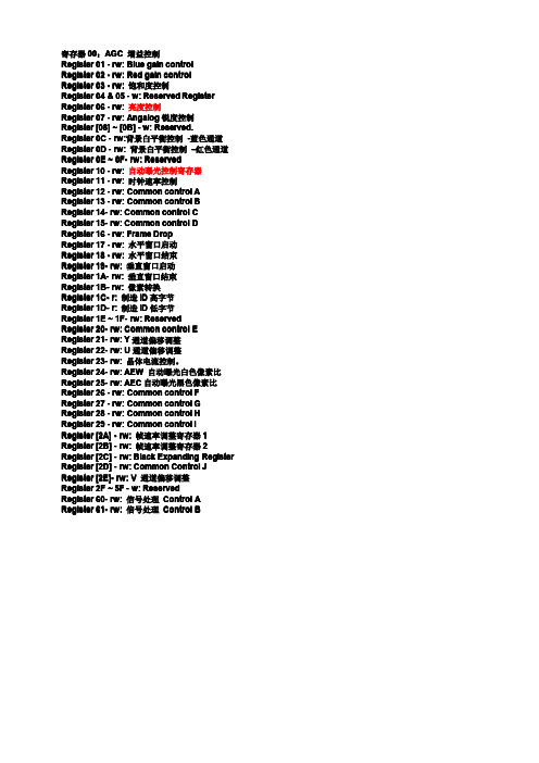
寄存器00:AGC增益控制Register01-rw:Blue gain controlRegister02-rw:Red gain controlRegister03-rw:饱和度控制Register04&05-w:Reserved Register Register06-rw:亮度控制Register07-rw:Angalog锐度控制Register[08]~[0B]-w:Reserved.Register0C-rw:背景白平衡控制-蓝色通道Register0D-rw:背景白平衡控制–红色通道0F--rw:ReservedRegister0E~0FRegister10-rw:自动曝光控制寄存器Register11-rw:时钟速率控制Register12-rw:Common control A Register13-rw:Common control B14--rw:Common control C Register1415--rw:Common control D Register15Register16-rw:Frame DropRegister17-rw:水平窗口启动Register18-rw:水平窗口结束Register19-rw:垂直窗口启动Register1A-rw:垂直窗口结束Register1B-rw:像素转换Register1C-r:制造ID高字节Register1D-r:制造ID低字节1F--rw:ReservedRegister1E~1F20--rw:Common control E Register2021--rw:Y通道偏移调整Register21Register22-rw:U通道偏移调整Register23-rw:晶体电流控制。
Register24-rw:AEW自动曝光白色像素比25--rw:AEC自动曝光黑色像素比Register25Register26-rw:Common control F Register27-rw:Common control G Register28-rw:Common control H Register29-rw:Common control IRegister[2A]-rw:帧速率调整寄存器1 Register[2B]-rw:帧速率调整寄存器2 Register[2C]-rw:Black Expanding Register Register[2D]-rw:Common Control J Register[2E]-rw:V通道偏移调整Register2F~5F-w:ReservedRegister6060--rw:信号处理Control A61--rw:信号处理Control B Register6162--rw:RGB Gamma ControlRegister62Register6363--rw:Reserved64--rw:Y Gamma ControlRegister6465--rw:信号处理Control CRegister6566--rw:AWB过程控制Register6667--rw:颜色空间选择Register6768--rw:信号处理Control DRegister6869--rw:模拟锐度Register696A--rw:垂直边缘增强控制Register6ARegister6B6B--6E rw:ReservedRegister6F-rw:偶/奇噪声补偿控制Register70-rw:Common Control KRegister71-rw:Common Control JRegister72-rw:水平同步第一边移Register73-rw:水平同步第二边移Register74-rw:Common Control MRegister75-rw:Common Control NRegister76-rw:Common Control ORegister77-7B-rw:ReservedRegister7C-rw:Field Average Level Storage寄存器00:AGC增益控制AGC<5:0>-增益设置为整个图像通道计算公式为:Gain=(AGC<3:0>/16+1)*(AGC<4>+1)*(AGC<5>+1);range(1x~7.75x),AGC<5>and AGC<4>control SA2.寄存器3:饱和度控制SAT<7:0>-saturation adjustment(饱和度调整)for the UV channel based on the default setting;80],减少SAT<<7:0>7:0><[<[<[80]范围(-4dB〜+6dB)。
OV6620有关的说明
OV6620有关的说明介绍一下数字摄像头OV6620的特征1)、OV6620需要稳定的5V电压供电,和系统板上的供电电源兼容。
2)、NAL制,每秒25帧,一帧两场,那么每秒就有50场。
意味着20MS就有一幅图像产生。
356x 292 pixels ,理解为:有292行,一行有356个点。
3)、视野和可视距离:这个和镜头的选择有关,f=3.6MM时视野应该有25度左右,f 越大视场.可视距离需要调节镜头对焦.经我测试可视距离可以看十几米,毕竟相素值只有10 万越小多,用单片机读可以看到3-4M的距离.这里解释一下为什么用单片机读会打折扣. 因为黑线宽度只有2.5CM,太远了黑线会很细,采点之后就分辩不出是噪声还是有用信号了. 在1米左右时, 黑线宽度可用8 个点表示.注:以上数据均是24MBUSCL下每行可取150个点时测得,没有翻转摄像头•4)、内部有IIC 可编程.可以调整摄像头的参数,比如最大灰度,对比度,暴光率控制等等. 其本质是SCC助议的寄存器写入,需要对摄像头做跳线处理,并用MCU勺I/O 口模拟SCC眇议.注:SCCB协议视作IIC协议,有些细微的差别•对IIC的写入,本文后面稍加说明• 5)、数据格式-YCrCb 4:2:2, GRB 4:2:2, RGB; 电子曝光/增益/白平衡控制;内部自动图像增强,亮度,对比度,伽马,饱和度,锐度,力卩窗等•最重要的是,不需AD,不需1881。
当然玩一下他的模拟输出一可以,VTO管脚就可以当普通模拟摄像头用.OV6620勺图像采集数字摄像头相对来说贵一些,他内部的信号处理比较复杂,接口也较多,一般是彩色的YUV信号,只取丫的亮度信号,所以用起来略有浪费•先看ov6620datasheet上的时序图:_ 刖帥Field ■切I L J Qtid Fiela:FODC-1)HREFValid DataHorlzontoi TirninnFOTJDHREF高为40u$,低为23uS饥lk为lltaS如果这个图还不明白的话看下面的说明PCLK遷L如果这个图还不明白的话看下面的这个图1、在采集时乎略TCLK首先是因为它太快了,捕捉不到,另外也没有必要捕捉到它。
ov7620介绍
CMOS图像传感器---OV7620图像采集时,为了减小的硬件复杂度,增强模块的独立性,采用HQ7620数字摄像头,它是基于Omnivsion公司的CMOS图像传感器---OV7620的方案设计的。
红树伟业1/3英寸(cmos芯片的大小)数字式CMOS图像传感器OV7620,总有效像素单元为664(水平方向)x492(垂直方向)像素;内置10位双通道A/ D转换器,输出8位图像数据;具有自动增益和自动白平衡控制,能进行亮度、对比度、饱和度、Y校正等多种调节功能;其视频时序产生电路可产生行同步、场同步、混合视频同步等多种同步信号和像素时钟等多种时序信号;5V电源供电,工作时功耗<120mW,待机时功耗<10uW。
能够满足本系统道路识别的要求。
CCD&CMOS:为什么不采用CCD传感器呢?CCD与CMOS传感器是被普遍采用的两种图像传感器,两者都是利用感光二极管(photodiode)进行光电转换,将图像转换为数字数据,而其主要差异是数字数据传送的方式不同。
CCD是采用连续扫描方式,即它只有等到最后一个像素扫描完成后才进行放大;CMOS传感器的每个像素都有一个将电荷放大为电信号的转换器。
所以CMOS的功耗比CCD要小。
由于CMOS功耗小,较CCD要便宜,而且图像质量满足要求。
(总之:CCD传感器在灵敏度、分辨率、噪声控制等方面都优于CMOS传感器,而CMOS传感器则具有低成本、低功耗、以及高整合度的特点。
)二值化传感器&OV7620:场地条件:瓷砖背景黑色赛道,极易受光照影子等光线变化影响,如果采用二值化传感器,只分成10个阈值,虽信息量小,但极易产生误判,本款红树伟业的OV7620模块提供了8个灰度Y的引脚,能识别256个灰度值,选择合适的考虑在分辨灰度的基础上的赛道颜色识别。
基本参数:大小:33x27x24(mm)电源:DC+5V ±5%扫描方式:逐行/隔行扫描最低照度:2.5 lux at f1.4 (3000k)信噪比:> 48 dB最大像素:(H)664 x (V)492;缺省有效像素:(H)640 x (V)480工作时功耗<120mW,待机时功耗<10uW;内置10位双通道A/ D转换器;输出8位图像数据;数据输出格式:YCrCb 16bit/8bit selectable:60Hz 16 Bit YCrCb 4:2:2 - 640x48060Hz 8 Bit YCrCb 4:2:2 - 640x480摄像头主要的采样格式有YCbCr 4:2:2(Y0 U0 Y1 V1 Y2 U2 Y3 V3 )、YCbCr 4:2:0(一行是4:2:0的话,下一行是4:0:2)、YCbCr 4:1:1(水平方向上对色度进行4:1抽样)和 YCbCr 4:4:4(三个分量信息完整)。
ov7620使用手册v1.1
HQ7620摄像头模块使用手册V1.1 2008.12 HQ7620V1.0版2009.1 HQ7620V1.1版重庆飞拓电子网()二〇〇九年一月资料如有更改,恕不另行通知一、模块概述HQ7620摄像头模块是基于Omnivision公司的CMOS图像传感器--- OV7620的方案设计;1/3英寸数字式CMOS图像传感器OV7620,总有效像素单元为664(水平方向)×492(垂直方向)像素;内置10位双通道A/D转换器,输出8位图像数据;具有自动增益和自动白平衡控制,能进行亮度、对比度、饱和度、γ校正等多种调节功能;其视频时序产生电路可产生行同步、场同步、混合视频同步等多种同步信号和像素时钟等多种时序信号;5V 电源供电,工作时功耗<120mW,待机时功耗<10μW。
可应用于数码相机、电脑摄像头、可视电话、第三代网络摄像机、手机、智能型安全系统、汽车倒车雷达、玩具,以及工业、医疗等多种用途。
OV7620是1/3”CMOS彩色/黑白图像传感器。
它支持连续和隔行两种扫描方式,VGA与QVGA两种图像格式;最高像素为664×492,帧速率为30fps;数据格式包括YUV、YCrCb、RGB三种,能够满足一般图像采集系统的要求。
HQ7620模块采用2.00mm双排插针接口,可以通过配送的双端2.00mm排线与其他应用连接(也可采用配送的单端2.54mm排线实现接口连接)HQ7620模块提供VTO测试输出,用户可以使用视频线连接到支持60Hz的电视或者视频卡测试效果。
HQ7620摄像头模块外观:基本参数:大小:33x27x24电源:DC+5V ±5%镜头:规格:1/3”;焦距: 3.6 ;光圈: 2.0 ;视角:92 ;技术参数:扫描方式:逐行/隔行扫描最低照度:2.5 lux at f1.4 (3000k)信噪比:> 48 dB最大像素:(H)664 x (V)492;缺省有效像素:(H)640 x (V)480数据输出格式:YCrCb 16bit/8bit selectable60Hz 16 Bit YCrCb 4:2:2 - 640x48060Hz 8 Bit YCrCb 4:2:2 - 640x480RGB Raw Data Digital Output 16Bit/8Bit selectableCCIR601, CCIR656, ZV 端口:支持8/16 位视频数据SCCB接口:最大速率支持400 kBit/sYCrCB或YUV输出格式:支持TV或监视器显示帧速率:可编程0.5~30fps逐行扫描模式:支持整个画面曝光支持亮度/对比度调节支持软件/硬件复位二、使用说明1、J1输出接口定义:名称属性说明1 SIO-1 I SCCB串行时钟输入2 SIO-0 I O SCCB串行数据3 Frex I 帧曝光控制输入4 CHSync/BW O/I 复合或水平同步信号输出/黑白模式是能输入5 Reset I 复位,高电平有效6 Y0/CBar O/I Y总线输出/Color Bar彩色条测试模式7 Y2/G2X O/I Y总线输出/Gain 2X8 Y1/PROG O/I Y总线输出/逐行扫描模式9 Y4/CS1 O/I Y总线输出/ SCCB从机模式ID配置位10 Y3/RAW O/I Y总线输出/Raw Data11 Y6/CS2 O/I Y总线输出/ SCCB从机模式ID配置位12 Y5/SHARP O/I Y总线输出/使能模拟Sharpness13 PCLK/OUTX2 O/I像素时钟输出/Doubles current output14 Y7/CSO O/I Y总线输出/SCCB从机模式ID配置位15 HRef/VSFram O/I 水平参考输出/垂直帧同步信号16 VSync/CSYS O/I 垂直同步信号/复合同步①信号地17 GND18 GND+5V电源输入19 VCC20 VCC21 UV1/CC656 O/I UV总线输出/CCIR 656模式22 UV0/GAMDis O/I UV总线输出/禁用色度伽玛23 UV3/ECLKO O/I UV总线输出/交换时钟输出②24 UV2/QVGA O/I UV总线输出/QVGA格式(320x240)25 UV5/MIR O/I UV总线输出/镜像26 UV4/SLAEN O/I UV总线输出/使能Slave27 UV7/B8 O/I UV总线输出/ 色度/亮度转换到8位模式③28 UV6/BPCLR O/I UV总线输出/旁路RGB色彩矩阵29 PWDN I PWDN =1 工作在掉电(睡眠)模式30 FODD/SRAM O/I 奇偶场标志/外部SRAM注:①复用为CSYS时,当不使用SCCB模式时,管脚42a(CHSYNC) 通过10k上拉电阻到CSYS;②当复用为ECLKO时,管教17(FODD)连接到XCLK输出;③色度/亮度默认为16位模式;2、J3:FREX输入控制端子;逐行扫描模式下有效;此管脚连接到排阵的pin3,此处保留了0欧接地电阻,如用户需要自己外部控制,可取消或者调整J3电阻。
OV7620 cmos摄像头的使用
OV7620 cmos摄像头的使用
OV7620简介ov7620是一款CMOS摄像头器件,是彩色CMOS型图像采集集成芯片,提供高性能的单一小体积封装,该器件分辨率可以达到640X480,传输速率可以达到30帧。
OV7620是1/3”CMOS彩色/黑白图像传感器。
它支持连续和隔行两种扫描方式,VGA与QVGA两种图像格式;最高像素为664×492,帧速率为30fps;数据格式包括YUV、YCrCb、RGB三种,能够满足一般图像采集系统的要求。
OV7620基本参数大小:33x27x24(mm)
电源:DC+5V±5%
扫描方式:逐行/隔行扫描
最低照度:2.5luxatf1.4(3000k)
信噪比:》48dB
最大像素:(H)664x(V)492;缺省有效像素:(H)640x(V)480
数据输出格式:
YCrCb16bit/8bitselectable
60Hz16BitYCrCb4:2:2-640x480
60Hz8BitYCrCb4:2:2-640x480
RGBRawDataDigitalOutput16Bit/8Bitselectable
CCIR601,CCIR656,ZV端口:支持8/16位视频数据
SCCB接口:最大速率支持400kBit/s
YCrCB或YUV输出格式:支持TV或监视器显示
摄像头工作原理按一定的分辨率,以隔行扫描的方式采集图像上的点,当扫描到某点时,就通过图像传感芯片将该点处图像的灰度转换成与灰度一一对应的电压值,然后将此电压值通过视频信号端输出。
具体而言(参见图5-1),摄像头连续地扫描图像上的一行,则输。