电容屏规格书
电解电容规格书22UF16V-4X5

20 min. 5 min.
D+0.5max.
工作電壓
16v
I≤3.52uA 充電 1 分鐘後
容量範圍
120Hz 20℃
17.6~26.4uf
使用溫度
-40~105℃
漏電流 uA
損失角正切值
120Hz 20℃
DF≤ 0.16
1.I≤標準值 2
等效阻抗
Ω≤
高溫負荷特性 1.I≤標準值 105℃加額定 電壓紋波 2000 小時
高頻低阻產品需測等效阻抗其它系列不要求此項sleevealcaselmax
規
格
22uf/16v
尺
寸
4*5
系
列
黑體白字 D: L: 4 5 1.5 0.5
TYPE’SDIMENSIONS(MM) 型狀及尺寸
SLEEVE AL.CASE d F 0.5
F: d:
L+ max. Safety vent ( 8 up) 6.3 is available by request
23.3 23.8 23.3 22.9 22.9 23.5 23.5 23.0 23.2 22.0
0.047 0.043 0.057 0.053 0.050 0.048 0.048 0.052 0.048 0.044
注:高頻低阻產品,需測等效阻抗,其它系列不要求此項
深圳市诚利来科技有限公司 Chengx Technology Co., Ltd.
Copyright © 2013
1/2
深圳市诚利来科技有限公司 Chengx Technology Co., Ltd.
Copyright © 2013
2/2
2.△C/C≤20% 3.△CF/CF≤ 200%
电解电容规格书63v4700UF

低温特性
错误!未找到引用源。 ≤5
四.铝电解电容器环境特性图
(1) 温度特性 C
.
DF
I
T 容量特性 损失值特性
T 漏电特性
T
(2) 频率特性 C DF I
T 容量特性 损失值特性
T 漏电特性T来自20 min. 5 min.
D+0.5max
F:
10
工作电压 漏电流
uA
63v
容量范围
120Hz 20℃
3800-540 0
使用温度
-40~105℃
I≤8883uA
充电 1 分钟后
损失角正切值
120Hz 20℃
DF≤ 0.08
高 温 特 性 1. I≤标准值 105 ℃ 加 电 2. △C/C≤30% 压 1000 小 3. △CF/CF≤30% 时
一. 结构(见附图)
NO. 1 2 3 4 5 6 7 8 9 部位 导针 引击线 胶塞 套管 外壳 正极箔 负极箔 隔离物 粘结体 材料 铝 99.99% 镀锡铜包钢线 三元异丙胶 PVC 热缩材料 铝 99.5% 氧化铝 99.99% 腐蚀铝 99.7% 电解纸 胶带或胶水
二.标志 商标(1) 规格(2) 负极标志(3) LTEC 4700UF63V
温度范围(4) 三.承认规格特性: 规 格 4700UF63V 尺 寸 22*40
-40 +105℃。
系
列 D: L: 22 40
TYPE’SDIMENSIONS(MM) 型状及尺寸
SLEEV
AL.CAS d F 0.
L max Safety vent ( 8 up) 6.3 is available by request
wima电容规格书

Polypropylene (PP) Film and Foil Capacitors for Pulse Applications in PCM 7.5 mm to 15 mmPulse duty constructionVery low dissipation factorNegative capacitance changeversus temperatureVery low dielectric absorptionAccording to RoHS 2002/95/ECTypical ApplicationsFor high frequency applications e.g.Sample and holdTimingLC-FilteringOscillating circuitsAudio equipmentDielectric:Polypropylene (PP) filmCapacitor electrodes:Metal foilInternal construction:Encapsulation:Solvent-resistant, flame-retardentplastic case with epoxy resin seal, UL94 V-0Terminations:Tinned wireMarking:Colour: Red. Marking: Black. Epoxyresin seal: Yellow.Capacitance range:100 pF to 0.22 μF(E12-values on request)Rated voltages:63VDC, 100VDC, 250VDC, 400VDC,630VDC, 1000VDCCapacitance tolerances:±20%, ±10%, ±5%Operating temperature range:-55°C to +100°CTest specifications:In accordance with IEC 60384-13 andEN 131800Climatic test category:55/100/56 in accordance with IECInsulation resistance at +20°C:> 5 x 10⁵ M(mean value: 1 x 10⁶ M)Measuring voltage:Ur = 63V: Utest = 50 V/1 min.Ur > 100V: Utest = 100 V/1 min.Dissipation factors at +20°C: tanTest voltage:2 Ur, 2 secMaximum pulse rise time:1000 V/μsec for pulses equal to the ratedvoltageDielectric absorption:0.05%Temperature coefficient:-200 x 10-6/°C (typical)Voltage derating:A voltage derating factor of 1.35% per Kmust be applied from +85°C for DC voltagesand from +75°C for AC voltages.Reliability:Operational life > 300000 hoursFailure rate < 5 fit (0.5 x Ur and40°C)Graphs:Soldering:Mechanical Tests PackingPull test on leads:10 N in direction of leads according toIEC 60068-2-21Vibration:6 hours at 10...2000Hz and 0.75mmdisplacement amplitude or 10g inaccordance with IEC 60068-2-6Low air density:Available taped and reeled.Detailed taping information:Example for ordering / Part number:1kPa = 10 mbar in accordance with IEC60068-2-13Bump test:4000 bumps at 390 m/sec2 inaccordance with IEC 60068-2-29Permissible AC voltagein relation to frequency at 10°C internal temperature rise (general guide)Polypropylene (PP) Capacitors for Pulse Applications with Double-Sided Metallized Electrodes and Schoopage Contacts inPCM 7.5 mm to 37.5 mmPulse duty constructionSelf-healingVery low dissipation factor Negative capacitance changeversus temperature According to RoHS 2002/95/ECTypical ApplicationsFor pulse applications e.g. Switch mode power suppliesTV and monitor setsLightingAudio/video equipmentConstructionDielectric:Capacitance range: 1000 pF to 15 μF (E12-values on request)Rated voltages:100VDC, 250VDC, 400VDC, 630VDC, 1000VDC, 1600VDC, 2000VDC,2500VDCCapacitance tolerances:±20%, ±10%, ±5% Operating temperature range:-55°C to +100°C Climatic test category: 55/100/56 in accordance with IEC Insulation resistance at +20°C: C < 0.33 μF: > 1 x 10⁵ MTest voltage: 1.6 Ur, 2 sec Dielectric absorption:0.05% Voltage derating:A voltage derating factor of 1.35% per K must be applied from +85°C for DCvoltages and from +75°C for AC voltages.Reliability:Operational life > 300000 hours Failure rate < 1 fit (0.5 x Ur and 40°C)Polypropylene (PP) filmCapacitor electrodes:Double-sided metallized plastic filmInternal construction:Encapsulation:Solvent-resistant, flame retardent plastic case with epoxy resin seal, UL 94 V-0Terminations:Tinned wireMarking:Colour: Red. Marking: Black. Epoxyresin seal: Red. (mean value: 5 x 10⁵ M)C > 0.33 μF: > 30000 sec (M xμF)(mean value: 100000 sec)Measuring voltage: 100V/1 min.Dissipation factors at +20°C: tanMechanical Tests PackingPull test on leads:d < 0.8 ?: 10 N in direction of leadsd > 0.8 ?: 20 N in direction of leadsaccording to IEC 60068-2-21Vibration:6 hours at 10...2000Hz and 0.75mmdisplacement amplitude or 10g inaccordance with IEC 60068-2-6Low air density:1kPa = 10 mbar in accordance with IEC60068-2-13Bump test:4000 bumps at 390 m/sec2 in accordancewith IEC 60068-2-29Available taped and reeled up to andincluding case size 15x26x31.5 / PCM27.5mm.Detailed taping information:Example for ordering / Part number:Permissible AC voltage in relation to frequency at 10°C internal temperature rise(general guide)。
江海电容器HPF系列导电高分子固体铝电解电容器规格书说明书

编号Issue No.G.HPF.202108022规格书版本号A客户版本号A0尊敬的Messrs规 格 书SPECIFICATIONS产品类型导电高分子固体铝电解电容器Product type Aluminium electrolytic capacitors with conductive polymer solid electrolyte产品系列HPFSeries南通江海电容器股份有限公司Nantong Jianghai Capacitor Co., Ltd.地址:江苏省南通市平潮镇通扬南路79号No.79 South Tongyang Road Pingchao TownNantong City Jiangsu Province PR ChinaTEL: 0086--0513--86726020 / FAX: 0086--0513--86571812日 期批 准审 核制 定Date Approved by Checked by Drawn by2021.8.5姚玉英孙何欢黄熊惑承认栏 User目录 ContentsNo.项目Item页码Page1适用范围 Scope42规格值 Specifications4~53尺寸 Dimensions54标志 Marking65构造 Structure76编码规则 Part number system77特性 Characteristics8~128包装 Packing139编带 Taping1410环保方面 Environmental1411使用注意事项 Technical note15~18G.HPF.202108022南通江海电容器股份有限公司 Nantong Jianghai Capacitor Co., Ltd.2规格书变更记录 (Change history of specification)发行日期版本原因内容页码标记发行编号Issued date Edition Reason Contents Page Mark Issue No.2021.8.5A 首次发行Original- 1 to 18-G.HPF.2021080221. 适用范围 Scope本规格书适用于HPF系列固体导电高分子铝电解电容器。
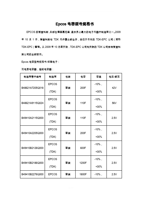
Epcos电容型号规格书
包装
电容
容差
电压-额定
B58031I5105M002
EPCOS (TDK)
带卷(TR)
1μF
±20%
305V
B58031I5105M62
EPCOS (TDK)
带卷(TR)
0.50μF
±20%
160V
B58031I7504M62
EPCOS (TDK)
带卷(TR)
1μF
±0.1pF
40V
B37923K5000B560
28V
B48621A7334Q018
EPCOS (TDK)
散装
13F
-10%,+30%
42V
B48621A7105Q018
EPCOS (TDK)
散装
100F
-10%,+30%
42V
电容器阵列:
制造商零件编号
制造商
包装
电容
容差
电压-额定
B37830R0330K021
EPCOS (TDK)
带卷(TR)
33pF
EPC±20%
63V
B43520B5108M
EPCOS (TDK)
散装
1000μF
±20%
450V
B43564A5108M
EPCOS (TDK)
散装
4700μF
±20%
450V
B43584E2478M
EPCOS (TDK)
散装
47000μF
±20%
200V
B41456B9479M
EPCOS (TDK)
带卷(TR)
10pF
±10%
25V
太诱电容规格书
25
±15%
C6
EIA X6S -55~+105
25
±22%
C7
EIA X7S -55~+125
25
±22%
LD(※)
EIA X5R -55~+ 85
25
JIS F
-25~+ 85
20
△F
EIA Y5V -30~+ 85
25
注:N※otLeD: 低※失.L真D 大Lo容w量di多st层or陶tio瓷n 电hig容h器value multilayer ceramic capacitor
⑧静Ca电pa容cit量an允ce许t偏ole差rance 代Co码de B C D F G J K M Z
C静a电pac容it量an允ce许to偏ler差ance ±0.1pF ±0.25pF ±0.5pF ±1pF ±2% ±5% ±10% ±20%
+80/-20%
⑨⑨产Th品ick厚ne度ss C代o码de C D P T K V W A D F G L N Y M
105
1.0+0.15/-0.05
0.5+0.15/-0.05
0.5+0.15/-0.05
107
1.6+0.20/-0
B
0.8+0.20/-0
0.45±0.05 0.8+0.20/-0 0.45±0.05
212
2.0+0.20/-0
1.25+0.20/-0
0.85±0.10
1.25+0.20/-0
316
C代o码de
Applicable 适st用an标dar准d
Temperature 温度ran范ge围[[℃℃] ]
R基e准f. T温em度p[.[℃℃]]
三星电容规格书
■INTRODUCTIONMLCC(Multilayer Ceramic Capacitor)is SMD(Surface Mounted Device)type capacitor that is used in wide ranges of capacitance.MLCC is paid more attentions than other capacitors due to the better frequency characteristics,higher reliability,higher withstanding voltage and so on.MLCC is made of many layers of ceramic and inner electrodes like sandwich.Pd was used for inner electrodes.But the price of Pd was skyrocketed and Pd was replaced by the BME(Base Metal Electrode),which reduced the total cost of MLCC.This inner electrode is connected to outer termination for surface mounting,which is composed of three layers,Cu or Ag layer,Ni plating layer,and SnPb or Sn plating layer.Most of MLCCs become Pb free by the environmental issue at present.MLCC is divided into two classes.Class I(C0G,etc)is the temperature compensating type.It hasa small TCC(Temperature Coefficient of Capacitance)and a better frequency performance.Therefore,it is used in RF applications such as cellular phone,tuner,and so on.Class II(X7R, X5R,Y5V,etc)is the high dielectric constant type,which is used in general electronic circuit.Especially high capacitance MLCC is replacing other capacitors(Tantalum and Aluminum capacitor)due to the low ESR(Equivalent Series Resistance)value.■FEATURE AND APPLICATION●Feature-Miniature Size-Wide Capacitance and Voltage Range-Highly Reliable Performance-Tape&Reel for Surface Mount Assembly-Low ESR-High Q at High Frequencies-Stable Temperature Dependence of Capacitance●Application-High Frequency Circuit(Tuner,VCO,PAM etc)-General Power Supply Circuit(SMPS etc)-DC-DC Converter-General Electronic Circuit■STRUCTURE■APPEARANCE AND DIMENSIONDIMENSION(mm)CODE EIA CODEL W T(MAX)BW 0302010.6±0.030.3±0.030.3±0.030.15±0.05050402 1.0±0.050.5±0.050.5±0.050.2+0.15/-0.1 100603 1.6±0.10.8±0.10.8±0.10.3±0.2210805 2.0±0.1 1.25±0.1 1.25±0.10.5+0.2/-0.3 311206 3.2±0.2 1.6±0.2 1.6±0.20.5+0.2/-0.3 321210 3.2±0.3 2.5±0.2 2.5±0.20.6±0.3431812 4.5±0.4 3.2±0.3 3.2±0.30.8±0.3552220 5.7±0.4 5.0±0.4 3.2±0.3 1.0±0.3■PREVIOUS PART NUMBERINGSymbol EIA Code TemperatureCoefficient(PPM/℃)※TemperatureCharacteristicsOperationTemperature RangeC C0G(CH)0±30C Δ-55~+125℃P P2H -150±60P ΔR R2H -220±60R ΔS S2H -330±60S ΔT T2H -470±60T ΔU U2J -750±120U ΔLS2L+350~-1000SL▶CLASS Ⅰ(Temperature Compensation)TemperatureCharacteristicsbelow 2.0pF 2.2~3.9pF above 4.0pFabove 10pFC ΔC0G C0G C0G C0G P Δ-P2J P2H P2H R Δ-R2J R2H R2H S Δ-S2J S2HS2H T Δ-T2J T2H T2H U Δ-U2JU2JU2JSymbol EIA Code Capacitance Change(ΔC :%)OperationTemperature RangeA X5R ±15-55~+85℃B X7R ±15-55~+125℃FY5V+22~-82-30~+85℃▶CLASS Ⅱ(High Dielectric Constant)SAMSUNG Multilayer Ceramic Capacitor Type(Size)Capacitance Temperature Characteristics Nominal Capacitance Capacitance Tolerance Rated Voltage Thickness Option Packaging Type CAPACITANCE TEMPERATURE CHARACTERISTICS ※Temperature Characteristics ☞K :±250PPM/℃J :±120PPM/℃H :±60PPM/℃G :±30PPM/℃●●●●●●●●●Temperature CharacteristicsSymbol Tolerance Applicable Capacitance &RangeC0G(NPO)or T.C SeriesB ±0.1pF 0.5~3pF C±0.25pF 0.5~10pF D ±0.5pF F ±1pF 6~10pFG ±2%E-24Series for over 10pF J ±5%K±10%A(X5R)B(X7R)J ±5%E-12SeriesK ±10%M ±20%F(Y5V)Z-20%~+80%E-6Series CAPACITANCE TOLERANCE The nominal capacitance value is expressed in pico-Farad(pF)and identified by three-digit number,first two digits represent significant figures and last digit specifies the number of zeros to follow.For values below 1pF,the letter "R"is used as the decimal point and the last digit becomes significant.example)100:10×10o =10pF 102:10×102=1000pF020:2×10o =2pF1R5:1.5pFNOMINAL CAPACITANCE ●●※Please consult us for special tolerances.RATED VOLTAGE ●PACKAGING TYPE THICKNESS OPTION Symbol Description of the CodeN Standard thickness (please refer to standard thickness table on next page)A Thinner than standard thickness B Thicker than standard thicknessC Standard Thickness High Q (Low `D.F `)D Sn-100%(High-Q)ESn-100%(General)※Please Consult us for other termination type.●●Series Capacitance StepE-3 1.02.24.7E-6 1.01.52.23.34.76.8E-12 1.0 1.2 1.5 1.8 2.2 2.7 3.3 3.9 4.7 5.6 6.88.2E-241.0 1.2 1.5 1.82.2 2.73.3 3.94.75.66.88.21.11.31.62.02.43.03.64.35.16.27.59.1※Standard Capacitance is "Each step ×10n "▶STANDARD CAPACITANCE STEP■NEW PART NUMBERING●PRODUCT ABBREVIATION Symbol Product AbbreviationCLSAMSUNG Multilayer Ceramic Capacitor●SIZE(mm)Symbol Size(mm)Length Width 030.60.305 1.00.510 1.60.821 2.0 1.231 3.2 1.632 3.2 2.543 4.5 3.2555.75.0SAMSUNG Multilayer Ceramic Capacitor Size(mm)Capacitance Temperature Characteristic Nominal Capacitance Capacitance Tolerance Rated Voltage Thickness Option Product &Plating Method Samsung Control Code Reserved For Future Use Packaging Type ●●●●●●●●●●●●CAPACITANCE TEMPERATURE CHARACTERISTICSymbol Temperature Characteristics Temperature RangeCClassⅠCOG C△0±30(ppm/℃)-55~+125℃P P2H P△-150±60R R2H R△-220±60S S2H S△-330±60T T2H T△-470±60U U2J U△-750±60L S2L S△+350~-1000AClassⅡX5R X5R±15%-55~+85℃B X7R X7R±15%-55~+125℃F Y5V Y5V+22~-82%-30~+85℃※Temperature CharacteristicTemperatureCharacteristicsBelow2.0pF 2.2~3.9pF Above4.0pF Above10pF CΔC0G C0G C0G C0GPΔ-P2J P2H P2HRΔ-R2J R2H R2HSΔ-S2J S2H S2HTΔ-T2J T2H T2HUΔ-U2J U2J U2JJ:±120PPM/℃,H:±60PPM/℃,G:±30PPM/℃●NOMINAL CAPACITANCENominal capacitance is identified by3digits.The first and second digits identify the first and second significant figures of the capacitance. The third digit identifies the multiplier.'R'identifies a decimal point.●ExampleSymbol Nominal Capacitance1R5 1.5pF10310,000pF,10nF,0.01μF104100,000pF,100nF,0.1μF●CAPACITANCE TOLERANCE Symbol Tolerance Nominal CapacitanceA ±0.05pF Less than 10pF (Including 10pF)B ±0.1pFC ±0.25pFD ±0.5pF F ±1pF F ±1%More than 10pF G ±2%J ±5%K ±10%M ±20%Z+80,-20%●RATEDVOLTAGE●THICKNESS OPTIONType Symbol Thickness(T)Spec 060330.30±0.03 100550.50±0.05 160880.80±0.102012A0.65±0.10 C0.85F 1.25±0.103216C0.85±0.15 F 1.25±0.15 H 1.6±0.203225F 1.25±0.20H 1.6I 2.0J 2.54532F 1.25±0.20H 1.6I 2.0J 2.5L 3.2±0.305750F 1.25±0.20H 1.6I 2.0J 2.5L 3.2±0.30●PRODUCT&PLATING METHODSymbol Electrode Termination Plating TypeA Pd Ag Sn_100%N Ni Cu Sn_100%G Cu Cu Sn_100%●SAMSUNG CONTROL CODE●RESERVED FOR FUTURE USESymbol Description of the codeN Reserved for future use●PACKAGING TYPE▶CAPACITANCE vs CHIP THICKNESS STANDARDDescription0603(0201)1005(0402)1608(0603)2012Type (0805)3216Type (1206)3225Type (1210)4532Type (1812)5750Type (2220)Dimension (mm)L0.6±0.03 1.0±0.05 1.6±0.1 2.0±0.13.2±0.153.2±0.2 3.2±0.34.5±0.45.7±0.4W 0.3±0.030.5±0.050.8±0.1 1.25±0.1 1.6±0.15 1.6±0.22.5±0.23.2±0.3 5.0±0.4T0.3±0.030.5~±0.050.8±0.10.65±0.10.85±0.11.25±0.10.85±0.15 1.25±0.15 1.6±0.21.25±0.2 1.6±0.22.0±0.22.5±0.21.25±0.21.6±0.22.0±0.22.5±0.21.6±0.22.0±0.22.5±0.2C A P ACIT A N CER A N G E (p F )SL 50V -0.5~2400.5~10000.5~10001100~15001600~27000.5~27003000~56006200~8200-----------C,TC (Except SL,UJ)25V 0.5~470.5~2200.5~1000--3300~82001500~36003900~68007500~10000-----100000-----50V -0.5~1800.5~10000.5~560620~10001100~33000.5~22002400~4700-560~1000011000~2200024000~47000-1000~1300015000~2200024000~4700062000~680004300093000130000C A P A C I T A N C E R A N G E (n F )A (X5R)6.3V 102202200--10000--10000---22000---47000--4700010V101001000--2200--4700~10000---22000------4700016V -47330~470--1000--4700---6800~10000-------25V --------------------50V- 6.8~10------------------B (X7R)6.3V 0.1~1047~100470~1000--1000--6800~10000---22000-------10V0.1~1033~100220~470220~270330~470560~1000-1000~330047001500~220033003900~4700----22000---16V0.1~110~33100~22068~200220~330390~1000330~6801000~15002200~33001500~220033003900~4700---2200----25V -4.7~1047~10039~6882~100150~470100~330470~620680~1000680~150018002200---1000---1000050V -0.22~4.70.22~1000.22~3947~1002201~150220390~1000 2.2~680820~1000--10~1000-----3300~4700F (Y5V)6.3V10~100-2200--10000-----47000--------10V -220~330100~1000--4700-470010000~22000---22000------10000016V -10~220100~100010~680820~10001200~22001000~22002700~4700100003300~68001000015000---22000----25V -10~3322~33010~220270~470560~1000470~10001200~22002700~33001000~33004700~10000-----10000---50V - 2.2~102.2~1002.2~6882~150180~100010~470560~1000-100~1000------10000---■PACKAGING●CARDBOARD PAPER TAPESymbol W F E P1P2P0D tABTypeD i m e n s i o n038.0±0.3 3.5±0.05 1.75±0.12.0±0.052.0±0.05 4.0±0.1Φ1.5+0.1/-00.37±0.030.38±0.030.68±0.03050.6±0.050.65+0.05/-0.1 1.15+0.05/-0.110 4.0±0.11.1MAX1.1±0.21.9±0.221 1.6±0.22.4±0.2312.0±0.23.6±0.2unit :mm●EMBOSSED PLASTIC TAPE●TAPING SIZE●REEL DIMENSIONSymbol A B CDEWtR7"Reel φ178±2.0min.φ50φ13±0.521±0.82.0±0.510±1.50.8±0.21.013"Reelφ330±2.0min.φ70unit :mmSymbol Cardboard Paper TapeEmbossed Plastic Tape7"Reel 4000200013"Reel15000-unit :pcsSize 05(0402)10(0603)21(0805)T ≤0.85mm T ≥1.0mm Quantity 50,00010,000~15,000*10,0005,000●BULK CASE PACKAGING-Bulk case packaging can reduce the stock space and transportation costs.-The bulk feeding system can increase the productivity.-It can eliminate the componentsloss.Symbol A B T C D E Dimension 6.8±0.18.8±0.112±0.1 1.5+0.1/-02+0/-0.14.7±0.1Symbol F W G H L I Dimension31.5+0.2/-036+0/-0.219±0.357±0.35110±0.75±0.35●QUANTITY*Option■CHARACTERISTIC MAP●CLASSⅠTemperature Characteristics Size VoltageCapacitance Range(㎊)SL,UJ05 (0402)50V10 (0603)50V21 (0805)50V31 (1206)50VC(COG)& TC Series03(0201)25V05(0402)25V50V10(0603)25V50V21(0805)25V50V31(1206)25V50V 32(1210)50V100V43(1812)25V50V55(2220)50V101001000100001000001000000100000001000000000.5240270082001000100010000150033004700100018022047820033001800047005604700068000100010000013000043000●CLASSⅡ,A(X5R)Temperature Characteristics Size Voltage Capacitance Range(㎊)A(X5R)0603(0201)6.3V10V1005(0402)6.3V10V16V50V1608(0603)6.3V10V16V2012(0805)6.3V10V16V3216(1206)6.3V10V16V3225(1210)6.3V10V16V4532(1812) 6.3V5750(2220)6.3V10V101001000100001000001000000100000001000000001000010000010000100000004700000220000002200000100000004700000220000004700000047000100006800100000022000001000000470000330000100000001000000068000004700000047000000220000●CLASSⅡ,B(X7R)Temperature Characteristics Size VoltageCapacitance Range(㎊)B(X7R)03(0201)6.3V10V16V05(0402)6.3V10V16V25V50V10(0603)6.3V10V16V25V50V21(0805)6.3V10V16V25V50V31(1206)6.3V10V16V 25V50V10100100010000100000100000010000000100000000100000470004700000470000100000100000047000022000010000003300000100000010000001001000010000000100000100000100100001001000680000033000100003300010000470047002204700002200002200001000004700022022000010000006800039000220100000033000010000010000001000●CLASSⅡ,B(X7R)Temperature Characteristics Size VoltageCapacitance Range(㎊)B(X7R)32(1210)6.3V10V16V25V50V43(1812)10V16V25V50V55(2220)25V50V1010010001000010000010000001000000010000000022000000100000010000470000015000002200000010000001000000047000003300000470000015000002200000680000100000022002200000●CLASSⅡ,F(Y5V)Temperature Characteristics Size VoltageCapacitance Range(㎊)F(Y5V)03(0201) 6.3V05(0402)10V16V25V50V10(0603)6.3V10V16V25V50V21(0805)6.3V10V16V25V50V31(1206)10V16V 25V50V32(1210)6.3V10V16V25V50V43(1812)16V25V50V55(2220)10V330000330001000022000010000220010000003300001000001000002200022001000000220000010000100002200000047000001000000033000001000000100000047000010000470000010000001500000033000001000000100000100000002200000010000220000100000001000000010000000022000001000000010000010000100000010000010000002200470000002200000010100100010000100000100000010000000100000000■RELIABILITY TEST DATANO ITEM PERFORMANCE TEST CONDITION 1APPEARANCE NO ABNORMAL EXTERIOR APPEARANCE THROUGH MICROSCOPE(×10)2INSULATIONRESISTANCE10,000㏁OR500㏁·㎌PRODUCT WHICHEVER ISSMALLER(RATED VOLTAGE IS BELOW16V:10,000㏁OR100㏁·㎌)RATED VOLTAGE SHALL BE APPLIED.MEASUREMENT TIME IS60~120RATED VOLTAGETIME60SEC.3WITHSTANDINGVOLTAGENO DIELECTRIC BREAKDOWN ORMECHANICAL BREAKDOWNCLASSⅠ:300%OF THE RATED VOLTAGE FOR1~5SEC,CLASSⅡ:250%OF THE RATED VOLTAGE FOR1~5SECIS APPLIED WITH LESS THAN50㎃CURRENT4CAPACITANCECLASSⅠWITHIN THE SPECIFIEDTOLERANCECAPACITANCE FREQUENCY VOLTAGE1,000㎊ANDBELOW1㎒±10%0.5~5VrmsMORE THAN1,000㎊1㎑±10%CLASSⅡWITHIN THE SPECIFIEDTOLERANCECAPACITANCE FREQUENCY VOLTAGE10㎌AND BELOW1㎑±10% 1.0±0.2VrmsMORE THAN10㎌120㎐±20%0.5±0.1Vrms5Q CLASSⅠOVER30㎊:Q≥1,000LESS THAN30㎊:Q≥400+20C(C:CAPACITANCE)CAPACITANCE FREQUENCY VOLTAGE1,000㎊ANDBELOW1㎒±10%0.5~5VrmsMORE THAN1,000㎊1㎑±10%6TanδCLASSⅡ1.CHAR:B2.CHAR:FCAPACITANCE FREQUENCY VOLTAGE10㎌AND BELOW1㎑±10% 1.0±0.2VrmsMORE THAN10㎌120㎐±20%0.5±0.1Vrms RATED VOLTAGE DF SPEC6.3V0.05max10V0.05max16V0.035max25V0.025max50V이상0.025max6.3V10V16V25V50V1005-0.125max0.09max(C<220nF)0.125max(C≥220nF)0.05max0.05max16080.16max0.125max0.09max0.05max(C≤100nF)0.07max(C>100nF)0.05max20120.16max0.125max0.09max0.07max0.05max32160.16max0.125max0.09max0.07max0.05max32250.16max0.125max0.09max0.07max(C≤6.8㎌)0.09max(C>6.8㎌)0.05max45320.16max0.16max0.09max--57500.125max---www.cdindustries.hk*THE INITIAL VALUE OF HIGH DIELECTRIC CONSTANT SERIES SHALL BE MEASUREDAFTER THE HEAT TREATMENT OF150+0/-10℃,1Hr AND SITTING OF48±4hr AT ROOM TEMPERATURE&ROOM HUMIDITY.NO ITEM PERFORMANCE TEST CONDITION14HUMIDITY(STEADYSTATE)APPEARANCE NO MECHANICAL DAMAGE SHALL OCCUR TEMPERATURE:40±2℃RELATIVE HUMIDITY:90~95%RHTEST TIME:500+12/-0Hr.MEASURE AT ROOM TEMPERATUREAFTER COOLING FORCLASSⅠ:24±2Hr.CLASSⅡ:48±4Hr.CAPACITANCECHARACTERISTIC CAPACITANCE CHANGECLASSⅠWITHIN±5%OR±0.5㎊WHICHEVERIS LARGERCLASSⅡA,B WITHIN±12.5%F WITHIN±30%QCLASSⅠ30㎊AND OVER:Q≥35010~30㎊:Q≥275+2.5×CLESS THAN10pF:Q≥200+10×CTanδCLASSⅡINSULATIONRESISTANCEMINIMUM INSULATION RESISTANCE:1,000㏁OR50㏁·㎌PRODUCT WHICHEVER ISSMALLER15MOISTURERESISTANCEAPPEARANCE NO MECHANICAL DAMAGE SHALL OCCUR APPLIED VOLTAGE:RATED VOLTAGETEMPERATURE:40±2℃RELATIVE HUMIDITY:90~95%RHTEST TIME:500+12/-0Hr.CURRENT APPLIED:50㎃MAX.<INITIAL MEASUREMENT>CLASSⅡSHOULD BE MEASUREDINITIAL VALUE AFTER BE HEAT-TREATEDFOR1HR IN150℃+0/-10℃AND BE LEFTFOR48±4HR AT ROOM TEMPERATURE.<LATTER MEASUREMENT>CLASSⅠSHOULD BE MEASURED AFTERLEFT FOR24±2HRS IN ROOMTEMPERATURE AND HUMIDITY.CLASSⅡSHOULD BE MEASUREDLATTER VALUE AFTER BEHEAT-TREATED FOR1HR IN150℃+0/-10℃AND BE LEFT FOR48±4HR AT ROOMTEMPERATURE.CAPACITANCECHARACTERISTIC CAPACITANCE CHANGECLASSⅠWITHIN±7.5%OR±0.75㎊WHICHEVERIS LARGERCLASSⅡA,B WITHIN±12.5%FWITHIN±30%WITHIN+30~-40%1005C>0.47μF1608C>1.0μF2012C>4.7μF3216C>10.0μF3225C>22.0μF4532C>47.0μFQCLASSⅠ30㎊AND OVER:Q≥20030㎊AND BELOW:Q≥100+10/3×CTanδCLASSⅡINSULATIONRESISTANCEMINIMUM INSULATION RESISTANCE:500㏁OR25㏁·㎌PRODUCT,WHICHEVER IS SMALLER.CHAR.25VANDOVER16V10V 6.3V4VA,B0.050.05MAX0.05MAX0.075MAX0.1MAXF0.075MAX0.1MAX(C〈1.0㎌)0.125MAX(C≥1.0㎌)0.15MAX0.195MAX0.25MAXCHAR.25VANDOVER16V10V 6.3V4VA,B0.05MAX0.05MAX0.05MAX0.075MAX0.1MAXF0.075MAX0.1MAX(C〈1.0㎌)0.125MAX(C≥1.0㎌)0.15MAX0.195MAX0.25MAX6.3VTanδ0.125MAX*ConditionCLASSⅡ(A,B)1005C≥0.22㎌1608C≥2.2㎌2012C≥4.7㎌3216C≥10.0㎌3225C≥22.0㎌4532C≥47.0㎌5750C≥100.0㎌6.3V Tanδ0.125MAX*ConditionCLASSⅡ(A,B)1005C≥0.22㎌1608C≥2.2㎌2012C≥4.7㎌3216C≥10.0㎌3225C≥22.0㎌4532C≥47.0㎌5750C≥100.0㎌NO ITEM PERFORMANCE TEST CONDITION16HIGHTEMPERATURERESISTANCEAPPEARANCE NO MECHANICAL DAMAGE SHALL OCCURAPPLIED VOLTAGE:150%,200%OF RATED VOLTAGETEST TIME:1000+48/-0Hr.CURRENT APPLIED:50㎃MAX.<INITIAL MEASUREMENT>CLASSⅡSHOULD BE MEASURED INITIALVALUE AFTER BE HEAT-TREATED FOR1HR IN150℃+0/-10℃AND BE LEFT FOR48±4HR AT ROOM TEMPERATURE.<LATTER MEASUREMENT>CLASSⅠSHOULD BE MEASURED AFTERLEFT FOR24±2HRS IN ROOMTEMPERATURE AND HUMIDITY.CLASSⅡSHOULD BE MEASURED LATTERVALUE AFTER BE HEAT-TREATED FOR1HR IN150℃+0/-10℃AND BE LEFT FOR48±4HR AT ROOM TEMPERATURE.(TWICE OF RATED VOLTAGE WILL BEAPPLIED TO ALL SERIES BUT ABOVE)**HOWEVER,A/B는1005C≥0.22㎌SEE(FIG.3)CAPACITANCECHARACTERISTIC CAP.CHANGECLASSⅠWITHIN±3%OR±0.3㎊,WHICHEVER IS LARGERCLASSⅡA,B WITHIN±12.5%FWITHIN±30%WITHIN+30~40%1005C>0.47μF1608C>1.0μF2012C>4.7μF3216C>10.0μF3225C>22.0μF4532C>47.0μFQCLASSⅠ30㎊AND OVER:Q≥35010~30㎊:Q≥275+2.5×CLESS THAN10㎊:Q≥200+10×CTanδCLASSⅡINSULATIONRESISTANCEMINIMUM INSULATION RESISTANCE:1,000㏁OR50㏁·㎌PRODUCTWHICHEVER IS SMALLER17TEMPERATURECYCLEAPPEARANCE NO MECHANICAL DAMAGE SHALL OCCUR CAPACITORS SHALL BE SUBJECTEDTO FIVE CYCLES OF THETEMPERATURE CYCLE AS FOLLOWINGSTEP TEMP.(℃)TIME(MIN)1MIN.RATEDTEMP.+0/-3302252~33MAX.RATEDTEMP.+3/-0304252~3MEASURE AT ROOM TEMPERATUREAFTER COOLING FORCLASSⅠ:24±2Hr.CLASSⅡ:48±4Hr.CAPACITANCECHARACTERISTIC CAP.CHANGECLASSⅠWITHIN±2.5%OR±0.25㎊WHICHEVER ISLARGERCLASSⅡA,B WITHIN±7.5%F WITHIN±20%QCLASSⅠ30㎊AND OVER:Q≥1000LESS THAN30㎊:Q≥400+20×CTanδCLASSⅡTO SATISFY THE SPECIFIEDINITIAL VALUEINSULATIONRESISTANCETO SATISFY THE SPECIFIEDINITIAL VALUECHAR.25VANDOVER16V10V 6.3V4VA,B0.05MAX0.05MAX0.05MAX0.075MAX0.1MAXF0.075MAX0.1MAX(C<1.0㎌)0.125MAX(C≥1.0㎌)0.15MAX0.195MAX0.25MAXCHAR.TEMP.CLASSⅠ125±3℃CLASSⅡA85±3℃B125±3℃F85±3℃*150%Authorization ConditionsCLASSⅡ(A,B,F)1005C>0.47μF1608C≥2.2㎌2012C≥4.7㎌3216C≥10.0㎌3225C≥22.0㎌4532C≥47.0㎌5750C≥100.0㎌■CHARACTERISTIC GRAPH▶CAPACITANCE CHANGE -AGING▶CAPACITANCE -DC VOLTAGE CHARACTERISTICS▶CAPACITANCE -TEMPERATURE CHARACTERISTICS●ELECTRICAL CHARACTERISTICS■APPLICATION MANUAL●Storage Condition▶Storage EnvironmentThe electrical characteristics of MLCCs were degraded by the environment of high temperature or humidity.Therefore,the MLCCs shall be stored in the ambient temperature and the relative humidity of less than40℃and70%,respectively.Guaranteed storage period is within6months from the outgoing date of delivery.▶Corrosive GasesSince the solderability of the end termination in MLCC was degraded by a chemical atmosphere such as chlorine,acid or sulfide gases,MLCCs must be avoid from these gases.▶Temperature FluctuationsSince dew condensation may occur by the differences in temperature when the MLCCs are taken out of storage,it is important to maintain the temperature-controlled environment.●Design of Land PatternWhen designing printed circuit boards,the shape and size of the lands must allow for theproper amount of solder on the capacitor.The amount of solder at the end terminations has a direct effect on the crack.The crack in MLCC will be easily occurred by the tensile stress which was due to too much amount of solder.In contrast,if too little solder is applied,the termination strength will be e the following illustrations as guidelines for proper land design.Recommendation of Land Shape and Size●AdhesivesWhen flow soldering the MLCCs,apply the adhesive in accordance with the following conditions.▶Requirements for AdhesivesThey must have enough adhesion,so that,the chips will not fall off or move during thehandling of the circuit board.They must maintain their adhesive strength when exposed to soldering temperature.They should not spread or run when applied to the circuit board.They should harden quickly.They should not corrode the circuit board or chip material.They should be a good insulator.They should be non-toxic,and not produce harmful gases,nor be harmful when touched.▶Application MethodIt is important to use the proper amount of adhesive.Too little and much adhesive will cause poor adhesion and overflow into the land,respectively.▶Adhesive hardening CharacteristicsTo prevent oxidation of the terminations,the adhesive must harden at160℃or less,within2minutes or less.●Mounting▶Mounting Head PressureExcessive pressure will cause crack to MLCCs.The pressure of nozzle will be300g maximum during mounting.▶Bending StressWhen double-sided circuit boards are used,MLCCs first are mounted and soldered onto one side of the board.When the MLCCs are mounted onto the other side,it is important to support the board as shown in the illustration.If the circuit board is not supported,the crack occur to the ready-installed MLCCs by the bending stress.●FluxAlthough the solderability increased by the highly-activated flux,increase of activity in flux may also degrade the insulation of the chip capacitors.To avoid such degradation,it is recommended that a mildly activated rosin flux(less than0.2%chlorine)be used.●SolderingSince a multilayer ceramic chip capacitor comes into direct contact with melted solder during soldering,it is exposed to potentially mechanical stress caused by the sudden temperature change.The capacitor may also be subject to silver migration,and to contamination by the flux.Because of these factors,soldering technique is critical.▶Soldering MethodsMethodClassificationReflow soldering-Overall heating-Infrared rays -Hot plate-VPS(vapor phase)-Local heating-Air heater -Laser-Light beamFlow soldering-Single wave -Double wave-*We recommend the reflow soldering method.▶Soldering ProfileTo avoid crack problem by sudden temperature change,follow the temperature profile in the adjacentgraph.30025020015010050℃Reflow Soldering 30025020015010050℃60~120sec 3~4secFlow Soldering▶Manual SolderingManual soldering can pose a great risk of creating thermal cracks in chip capacitors.The hotsoldering iron tip comes into direct contact with the end terminations,and operator's carelessnessmay cause the tip of the soldering iron to come into direct contact with the ceramic body of the capacitor.Therefore the soldering iron must be handled carefully,and close attention must be paid to the selection of the soldering iron tip and to temperature control of the tip.▶Amount ofSolder▶CoolingNatural cooling using air is recommended.If the chips are dipped into solvent for cleaning, the temperature difference(△T)must be less than100℃6-6.CleaningIf rosin flux is used,cleaning usually is unnecessary.When strongly activated flux is used, chlorine in the flux may dissolve into some types of cleaning fluids,thereby affecting the chip capacitors.This means that the cleaning fluid must be carefully selected,and should always be new.▶Notes for Separating Multiple,Shared PC Boards.A multi-PC board is separated into many individual circuit boards after soldering has been completed.If the board is bent or distorted at the time of separation,cracks may occur in the chip capacitors.Carefully choose a separation method that minimizes the bending of the circuit board.■CROSS REFERENCEP/N COMPANY SAMSUNG AVX JOHANSON KEMET KYOCERA MURATA NOVACAP PANASONIC ROHMTAIYO-YUDENTDK VITRAMON①COMPANY MODEL(MLCC)CL--C CM GRM-ECJ MCH MK C VJ②SIZE (EIA/JIS)0201(0603)03---0333-Z-0630603-0402(1005)050402R0704020536040201510510050402 0603(1608)100603R14060310539060311810716080603 0805(2012)210805R1508052140080522121220120805 1206(3216)311206R181********-6120633131632161206 1210(3225)321210S4112103242-2121043232532251210 1808(4520)421808R29180842-1808---45201808 1812(4532)431812S4318124343-21812-4343245321812 2220(5750)55--22205544-12221--5505650-③TEMPERATURE CHARACTERISTIC COG(NPO)C A N G CG COG/CH N C A C COG/CH A P2H(N150)P S--P P2H-P-P PH-R2H(N220)R1--R R2H-R-R RH-S2H(N330)S3--S S2H-S-S SH-T2H(N470)T O--T T2H-T-T TH-U2J(N750)U Z--U U2J-U UJ U UJ-S2L L Y--SL SL-G SL SL SL-X7R B C W R(X)X7R X7R B B C BJ X7R(B)Y(X) Z5U E E Z U-Z5U Z-E-Z5U U Y5V F G Y V Y5V Y5V Y F F F Y5V-④NOMINAL CAPACITANCE EX)103=10,000㎊221=220㎊225=2,200,000㎊=2.2㎌1R5=1.5㎊010=1㎊⑤CAPACITANCE TOLERANCE B:±0.1㎊C:±0.25㎊D:±0.5㎊F:±1%G:±2%J:±5%K:±10%M:±20%Z:-20~+80%⑥RATED VOLTAGE6.3V Q6-906 6.3-0J-J0J-10V P Z10081010-1A4L1A-16V O Y160416161601C3E1C J 25V A3250325252501E2T1E X 50V B5500550505001H5U1H A 100V C110111*********A1-2A B 200V D220122002002012D---C 250V E V--250250251---2E-500V G7501-500500501----E 630V H---630630----2J-1000V I A102-10001K102---3A G 2000V J G202-20002K202---3D-3000V K H302-30003K302---3F H 4000V-J-4000-402-----⑦TERMINATIONNICKEL BARRIER N T V C A(GRM)N-(MCH)--X Ag/Pd P1--B(GR)P-(MC)--F⑧PACKAGEBULK(VINYL)B9(NONE)-B PB*X-B B B PAPER TAPING C2,4T,R-T,L PT T E,V,W K,L T T C,P PLASTIC TAPING E1,3E,U-H,N PT-F,Y P,Q T-T,R BULK CASE P7--C PC-C C--G。
39uf 电解电容规格书
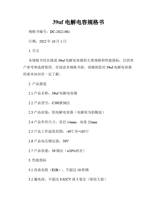
39uf 电解电容规格书规格书编号:DC-2022-001日期:2022年10月1日1. 引言本规格书旨在描述39uf电解电容器的主要规格和性能指标,以供客户参考和选择使用。
在阅读本规格书前,请确保您对39uf电解电容器的基本知识有一定了解。
2. 产品描述2.1 产品名称:39uf 电解电容器2.2 产品型号:C39UF20222.3 产品封装:铝电解电容器(电解质为铝酸盐)2.4 产品外形尺寸:直径14mm,高度25mm2.5 产品工作温度范围:-40℃至+105℃2.6 产品电压额定值:50V2.7 产品容量:39微法(±20%容差)3. 性能指标3.1 直流电阻(ESR):不超过10欧姆3.2 漏电流:不超过0.02CV或3毫安(取较大值)3.3 最大涟漪电流:30毫安有效值3.4 寿命:5000小时(温度为105℃,涟漪电流为最大涟漪电流时)3.5 极性:正极带标记,负极为未标记一端3.6 绝缘电阻:1000兆欧姆或者RC×C(μF),以较小值为准(其中RC为产品额定电压)4. 安装与使用建议4.1 安装电解电容器时,请确保极性正确。
否则,可能会导致电容器损坏或电路故障。
4.2 在使用39uf电解电容器时,请尽量避免超过额定电压和温度范围,以延长产品使用寿命。
4.3 当电容器长时间未使用时,请断开其电源并将其储存于低温、低湿度环境中,以保持其性能和寿命。
5. 产品认证与标准5.1 本产品符合国际电工委员会(IEC)的IEC 60384-1标准要求。
5.2 此外,本产品还通过了ISO 9001质量管理体系认证。
6. 包装与交货6.1 39uf电解电容器将被包装在防静电袋中,以防止静电对产品造成损害。
6.2 产品交货将按照双方协商的时间和地点进行。
7. 售后服务7.1 对于质量问题,请在收到产品后的7个工作日内与我们联系,我们将提供免费的维修或更换服务。
7.2 对于非质量问题的退货和更换,需按照公司规定的退换货流程进行。
- 1、下载文档前请自行甄别文档内容的完整性,平台不提供额外的编辑、内容补充、找答案等附加服务。
- 2、"仅部分预览"的文档,不可在线预览部分如存在完整性等问题,可反馈申请退款(可完整预览的文档不适用该条件!)。
- 3、如文档侵犯您的权益,请联系客服反馈,我们会尽快为您处理(人工客服工作时间:9:00-18:30)。
9
ID
Requirement IC LEDA LED CIRCUIT DIAGRAM LEDK
O CA (100um) TOP ITO FILM (125um)
FT6236GMA Surface Hardness Light Transmission Operating Temperature Storage Temperature Operating Humidty Storage Humidity 6H(750g) ≥ 85% -20~70℃ -30~80 ℃ 45~85 RH 45~95 RH
12 O'CLOCK
* * *
*8.66
15
MIPI_D1P
16
MIPI_D1N
JIANGXI HOLITECH TECHNOLOGY CO.,LTD
C over Glass T= 0.70mm IT O FILM T= 0.125mm
17
GND
18
CLK_P
19
OCA T = 0.1mm
*2.35±0.1 * 3.64
侧视图
背视图
IR区域(紫色): 可见光 550 nm处透过率4%-10%; 红外光 850 nm处透过率75%以上 元件区IC增加UV点胶 元件区覆黄 色高温胶纸 1.35mm MAX 3.20
孔 ?2 .8 0
*
PI+FPC厚度
* *
PI补强T=0.2mm 17.85±0.50 喷码区域 弯折区需柔化,正反面贴EMI
CLK_N
* 26.31
不透光 0.43± 0.05 9.89 * 6.26 0.30± 0.05 0.25± 0.05 6.97
冷灰6C,
20
* * * 6.72 *
GND
21
MIPI_D0P
7.93
22
* 9.96
MIPI_D0N
* *
*0.50(LCD AA TO TP VA) 18.06
*
23
正面保护膜 T= 0.06
BOTTOM
7
IOVCC
8
IOVCC
* 7.24± 0.3
9
自由高度0.4 工作高度0.325 TESA4972+PLM-03泡棉 +TESA4972
FPC对位线
GND
10
TE
11
RESET
12
*109.00± 0.15(BL)
PWM_OUT
*6.50
14
FPC外形
GND
丝印黑色
SPECIFICATION
Revision: V0 Product Model: KBF6118-4.5
Designed by CJ R&D Checked by JS Quality Department by ZW Approved by WCJ
Approval by Customer
OK NG,Problem survey:
元件区
*
4.60 * 18.99 *
*
*
高温胶纸 元件区 FR4补强 (不 含FPC)
防尘保护膜撕手
3.70
3
NC
*6.60±0.3
4
超 出FPC 1-2mm
VCC
* 11.70
通孔, C=0.15±0.05mm
双面胶 T = 0.05 (用于固定 FPC&CG)
*1.31min
5
VCC
6
NC
TOP
All Rights Reserved
1/20
JIANGXI HOLITECH TECHNOLOGY CO.,LTD
Revision record
VEV NO. V0 REV DATE 2015-09-01 NEW CONTENTS Note
All Rights Reserved
2/20
JIANGXI HOLITECH TECHNOLOGY CO.,LTD
Table Of Contents
List Description Cover Revision Record Table Of Contents 1 2 3 4 5 6 7 8 9 10 11 12 13 General Information External Dimensions Interface Description Absolute Maximum Ratings Electrical Characteristics Timing Characteristics Backlight Characteristics Optical Characteristics Reliability Test Conditions And Methods Inspection Standard Handling Precautions Precaution For Use Packing Method Page No. 1 2 3 4 5 6 7 7 8 11 11 15 16 19 20 20
Contents
64.20(H)x131.20(V)x3.60(T) 55.44(H)x98.637(V) 4.46 0.1155(H)x0.1155(V) RGB Vertical stripe 16.7M Normal White 12 O'CLOCK A-Si TFT --
Unit
mm mm dot inch mm g
Display resolution(dot) 480(H)x3(RGB)x854(V)
All Rights Reserved
4/20
:
A
DESCRIPTION
DATE
NAME
初始版本
08.06
YP
正视图
* *
5.50±0.05 * 4.50±0.05 * 0.50±0.05 * 0.30±0.05 * 0.50±0.10 * 0.3±0.03mm 1.30± 0.30 2.50± 0.30 白色对位线 W=0.2mm 8.20±0.30 1.50± 0.30
Approved By
1. If there is no special request from customer, holitech Co.,ltd. Will not reserve the tooling of the product under the following conditions: 1.1 There is no response from customer in one year after holitech Co.,ltd.Submit the samples; 1.2 There is no order in one year after the latest mass production. 2. All correlated data (include holitech record) will be reserved one year more after tooling was discarded. 3. If there is no special request from customer, The product of holitech Co.,ltd. Will repair only one year.
GND
5/20
99.64(LENS VA)
98.64(LCD AA)
480 X RGB854 4.46" TFT
131.20± 0.05(LENS OD)
13
GND
JIANGXI HOLITECH TECHNOLOGY CO.,LTD
3. Interface Description
Pin No. 1 2 3 4 5 6 7 8 9 10 11 12 13 14 15 16 17 18 19 20 21 22 23 24 25 26 27 28 29 30 31 32 33 Symbol GND LCM_ID NC VCC VCC NC IOVCC IOVCC GND TE RESET PWM_OUT GND GND MIPI_D1P MIPI_D1N GND CLK_P CLK_N GND MIPI_D0P MIPI_D0N GND GND CTPLEDK LEDA NC GND GND NC LEDK CTPLEDA GND Description Ground LCM read ID No connect Power supply(2.8V) Power supply(2.8V) No connect Power supply(1.8V) Power supply(1.8V) Ground Tearing effect out put pin Reset pin The PWM frequency output for LED driver control Ground Ground Positive MIPI Data 1 Input Negative MIPI Data 1 Input Ground Positive MIPI Clock Input Negative MIPI Clock Input Ground Positive MIPI Data 0 Input Negative MIPI Data 0 Input Ground Ground TP LED cathode LED anode No connect Ground Ground No connect LED cathode TP LED anode Ground
All Rights Reserved
3/20
JIANGXI HOLITECH TECHNOLOGY CO.,LTD
1. General Information
NO