MMSZ5228B-F中文资料
MMSZ5235B
Type Number
MMSZ5221B MMSZ5223B MMSZ5225B MMSZ5226B MMSZ5227B MMSZ5228B MMSZ5229B MMSZ5230B MMSZ5231B MMSZ5232B MMSZ5233B MMSZ5234B MMSZ5235B MMSZ5236B MMSZ5237B MMSZ5238B MMSZ5239B MMSZ5240B MMSZ5241B MMSZ5242B MMSZ5243B MMSZ5244B MMSZ5245B MMSZ5246B MMSZ5248B MMSZ5250B MMSZ5251B MMSZ5252B MMSZ5253B MMSZ5254B MMSZ5255B MMSZ5256B MMSZ5257B MMSZ5258B MMSZ5259B
6.30
20
6.2
5.89
6.51
20
6.8
6.46
ቤተ መጻሕፍቲ ባይዱ
7.14
20
7.5
7.13
7.88
20
8.2
7.79
8.61
20
8.7
8.27
9.14
20
9.1
8.65
9.56
20
10
9.50
10.50
20
11
10.45
11.55
20
12
11.40
12.60
20
13
12.35
13.65
9.5
14
13.30
14.70
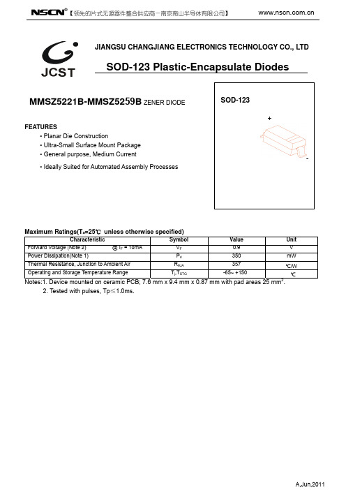
【领先的片式无源器件整合供应商—南京南山半导体有限公司】
JIANGSU CHANGJIANG ELECTRONICS TECHNOLOGY CO., LTD
MMSZ5242中文资料

Cathode Mark
.152 (3.85) .140 (3.55) .112 (2.85) .100 (2.55)
Top View
max. .004 (0.1)
max. .053 (1.35)
min. .010 (0.25)
max. .006 (0.15)
.067 (1.70) .055 (1.40)
50 25 15 10 5.0 5.0 5.0 5.0 5.0 5.0 3.0 3.0 3.0 3.0 3.0 3.0 2.0 1.0 0.5 0.1 0.1 0.1 0.1 0.1 0.1 0.1 0.1 0.1 0.1 0.1 0.1 0.1 0.1 0.1 0.1 0.1 0.1 0.1 0.1 0.1 0.1 0.1 0.1
1.0 1.0 1.0 1.0 1.0 2.0 2.0 3.0 3.5 4.0 5.0 6.0 6.5 6.5 7.0 8.0 8.4 9.1 9.9 10 11 12 13 14 14 15 17 18 19 21 21 23 25 27 30 33 36 39 43 46 47 52 56
NOTES: (1) The Zener Impedance is derived from the 1kHz AC voltage which results when an AC current having an RMS value equal to 10% of the Zener current (IZT or IZK) is superimposed on IZT or IZK. Zener Impedance is measured at two points to insure a sharp knee on the breakdown curve and to eliminate unstable units. (2) Measured with device junction in thermal equilibrium.
稳压二极管规格书资料

MMSZ5221BT1 SeriesPreferred DeviceZener Voltage Regulators 500 mW SOD−123 Surface MountThree complete series of Zener diodes are offered in the convenient, surface mount plastic SOD−123 package. These devices provide a convenient alternative to the leadless 34−package style.Features•500 mW Rating on FR−4 or FR−5 Board•Wide Zener Reverse V oltage Range − 2.4 V to 110 V •Package Designed for Optimal Automated Board Assembly •Small Package Size for High Density Applications •General Purpose, Medium Current•ESD Rating of Class 3 (>16 kV) per Human Body Model•Pb−Free Packages are AvailableMechanical CharacteristicsCASE:V oid-free, transfer-molded, thermosetting plastic case FINISH:Corrosion resistant finish, easily solderableMAXIMUM CASE TEMPERATURE FOR SOLDERING PURPOSES: 260°C for 10 SecondsPOLARITY:Cathode indicated by polarity band FLAMMABILITY RATING:UL 94 V−0MAXIMUM RATINGSMaximum ratings are those values beyond which device damage can occur. Maximum ratings applied to the device are individual stress limit values (not normal operating conditions) and are not valid simultaneously. If these limits are exceeded, device functional operation is not implied, damage may occur and reliability may be affected.1.FR−5 = 3.5 X 1.5 inches, using the minimum recommended footprint.2.Thermal Resistance measurement obtained via infrared Scan Method.See specific marking information in the device marking column of the Electrical Characteristics table on page 3 of this data sheet.DEVICE MARKING INFORMATIONDevices listed in bold, italic are ON Semiconductor Preferred devices. Preferred devices are recommended choices for future use and best overall value.ELECTRICAL CHARACTERISTICS (T A = 25°C unlessotherwise noted, V= 0.95 V Max. @ I = 10 mA)4.Nominal Zener voltage is measured with the device junction in thermal equilibrium at T L = 30°C $1°C.5.Z ZT and Z ZK are measured by dividing the AC voltage drop across the device by the ac current applied.The specified limits are for I Z(AC) = 0.1 I Z(dc) with the AC frequency = 1 KHz.V Z , NOMINAL ZENER VOLTAGE (V)−1012345678Figure 1. Temperature Coefficients (Temperature Range −55°C to +150°C)100101V Z , NOMINAL ZENER VOLTAGE (V)Figure 2. Temperature Coefficients (Temperature Range −55°C to +150°C)1.21.00.80.60.40.20T, TEMPERATURE (°C)Figure 3. Steady State Power Derating PW, PULSE WIDTH (ms)Figure 4. Maximum Nonrepetitive Surge Power1000100101V Z , NOMINAL ZENER VOLTAGEFigure 5. Effect of Zener Voltage onZener Impedance100101V F , FORWARD VOLTAGE (V)Figure 6. Typical Forward Voltage1000100101q V Z , T E M P E R A T U R E C O E F F I C I E N T (m V /°C )q V Z , T E M P E R A T U R E C O E F F I C I E N T (m V /°C )P p k , P E A K S U R G E P O W E R (W A T T S )Z Z T , D Y N A M I C I M P E D A N C E (W )I F , F O R W A R D C U R R E N T (m A )C , C A P A C I T A N C E (p F )V Z , NOMINAL ZENER VOLTAGE (V)Figure 7. Typical Capacitance 1000100101V Z , ZENER VOLTAGE (V)1001010.10.01V Z , ZENER VOLTAGE (V)1001010.10.01V Z , NOMINAL ZENER VOLTAGE (V)Figure 8. Typical Leakage CurrentFigure 9. Zener Voltage versus Zener Current(V Z Up to 12 V)Figure 10. Zener Voltage versus Zener Current(12 V to 91 V)I R , L E A K A G E C U R R E N T (m A )I Z , Z E N E R C U R R E N T (m A )I Z , Z E N E R C U R R E N T (m A )PACKAGE DIMENSIONSSOD−123CASE 425−04ISSUE Cǒmm inchesǓSCALE 10:1*For additional information on our Pb−Free strategy and solderingdetails, please download the ON Semiconductor Soldering and Mounting Techniques Reference Manual, SOLDERRM/D.SOLDERING FOOTPRINT*ON Semiconductor and are registered trademarks of Semiconductor Components Industries, LLC (SCILLC). SCILLC reserves the right to make changes without further notice to any products herein. SCILLC makes no warranty, representation or guarantee regarding the suitability of its products for any particular purpose, nor does SCILLC assume any liability arising out of the application or use of any product or circuit, and specifically disclaims any and all liability, including without limitation special, consequential or incidental damages.“Typical” parameters which may be provided in SCILLC data sheets and/or specifications can and do vary in different applications and actual performance may vary over time. All operating parameters, including “Typicals” must be validated for each customer application by customer’s technical experts. SCILLC does not convey any license under its patent rights nor the rights of others. SCILLC products are not designed, intended, or authorized for use as components in systems intended for surgical implant into the body, or other applications intended to support or sustain life, or for any other application in which the failure of the SCILLC product could create a situation where personal injury or death may occur. Should Buyer purchase or use SCILLC products for any such unintended or unauthorized application, Buyer shall indemnify and hold SCILLC and its officers, employees, subsidiaries, affiliates,and distributors harmless against all claims, costs, damages, and expenses, and reasonable attorney fees arising out of, directly or indirectly, any claim of personal injury or death associated with such unintended or unauthorized use, even if such claim alleges that SCILLC was negligent regarding the design or manufacture of the part. SCILLC is an Equal Opportunity/Affirmative Action Employer. This literature is subject to all applicable copyright laws and is not for resale in any manner.PUBLICATION ORDERING INFORMATION。
MMSZ5256资料
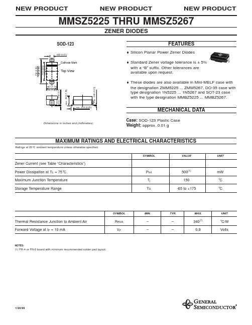
Cathode Mark
.152 (3.85) .140 (3.55) .112 (2.85) .100 (2.55)
Top View
max. .004 (0.1)
max. .053 (1.35)
min. .010 (0.25)
max. .006 (0.15)
.067 (1.70) .055 (1.40)
1/20/99
元器件交易网
MMSZ5225 THRU MMSZ5267
ELECTRICAL CHARACTERISTICS
Ratings at 25°C ambient temperature unless otherwise specified.
Type
Marking Code
1.0 1.0 1.0 1.0 1.0 2.0 2.0 3.0 3.5 4.0 5.0 6.0 6.5 6.5 7.0 8.0 8.4 9.1 9.9 10 11 12 13 14 14 15 17 18 19 21 21 23 25 27 30 33 36 39 43 46 47 52 56
NOTES: (1) The Zener Impedance is derived from the 1kHz AC voltage which results when an AC current having an RMS value equal to 10% of the Zener current (IZT or IZK) is superimposed on IZT or IZK. Zener Impedance is measured at two points to insure a sharp knee on the breakdown curve and to eliminate unstable units. (2) Measured with device junction in thermal equilibrium.
MMSZ5231中文资料

NEW PRODUCT
NEW PRODUCT
MMSZ5225 THRU MMSZ5267
ZENER DIODES
SOD-123
.022 (0.55)
FEATURES
♦ Silicon Planar Power Zener Diodes ♦ Standard Zener voltage tolerance is ± 5% with a “B” suffix. Other tolerances are available upon request. ♦ These diodes are also available in Mini-MELF case with the designation ZMM5225 ... ZMM5267, DO-35 case with type designation 1N5225 ... 1N5267 and SOT-23 case with the type designation MMBZ5225 ... MMBZ5267.
(%/K)
IR (µA)
Test Voltage VR (V)
MMSZ5225 MMSZ5226 MMSZ5227 MMSZ5228 MMSZ5229 MMSZ5230 MMSZ5231 MMSZ5232 MMSZ5233 MMSZ5234 MMSZ5235 MMSZ5236 MMSZ5237 MMSZ5238 MMSZ5239 MMSZ5240 MMSZ5241 MMSZ5242 MMSZ5243 MMSZ5244 MMSZ5245 MMSZ5246 MMSZ5247 MMSZ5248 MMSZ5249 MMSZ5250 MMSZ5251 MMSZ5252 MMSZ5253 MMSZ5254 MMSZ5255 MMSZ5256 MMSZ5257 MMSZ5258 MMSZ5259 MMSZ5260 MMSZ5261 MMSZ5262 MMSZ5263 MMSZ5264 MMSZ5265 MMSZ5266 MMSZ5267
MMSZ5229B-7-F中文资料

Lead-freeMMSZ5221B - MMSZ5259B500mW SURFACE MOUNT ZENER DIODE·500mW Power Dissipation ·General Purpose, Medium Current·Ideally Suited for Automated Assembly Processes ·Lead Free/RoHS Compliant (Note 2)·Qualified to AEC-Q101 Standards for High ReliabilityMechanical DataFeatures·Case: SOD-123·Case Material: Molded Plastic. UL Flammability Classification Rating 94V-0·Moisture Sensitivity: Level 1 per J-STD-020C ·Terminals:Solderable per MIL-STD-202, Method 208·Lead Free Plating (Matte Tin Finish annealed over Alloy 42leadframe)·Polarity: Cathode Band·Ordering Information: See Page 2·Marking: See Below·Weight: 0.01 grams (approximate)Maximum Ratings@ T A = 25°C unless otherwise specifiedNotes: 1. Device mounted on ceramic PCB; 7.6 mm x 9.4 mm x 0.87 mm with pad areas 25 mm 2.2. No purposefully added lead.Date Code KeyXX = Product Type Marking Code (See Page 2)YM = Date Code Marking Y = Year (ex: N = 2002)M = Month (ex: 9 = September)Marking InformationNotes: 3. f = 1KHz.4. Short duration test pulse used to minimize self-heating effect.Ordering Information(Note 5)* Add “-7-F” to the appropriate type number in Table 1 above example: 6.2V Zener= MMSZ5234B-7-F. Notes: 5. For Packaging Details, go to our website at /datasheets/ap02007.pdf.00.10.20.30.40.5255075100125150P ,P O W E R D I S S I P A T I O N (W )D T ,AMBIENT TEMPERATURE (C)Fig.1Power Dissipation vs Ambient TemperatureA °0.6C ,T O T A L C A P A C I T A N C E (p F )T 101001000101001V ,NOMINAL ZENER VOLTAGE (V)Fig.2Total Capacitance vs Nominal Zener VoltageZ102030405012345678910I ,Z E N E R C U R R E N T (m A )Z V ,ZENER VOLTAGE (V)Fig.4Zener Breakdown CharacteristicsZ1101001000110100V ,NOMINAL ZENER VOLTAGE (V)Fig.3Zener Voltage vs.Zener ImpedenceZ 0102030I ,Z E N E R C U R R E N T (m A )Z V ,ZENER VOLTAGE (V)Fig.5Zener Breakdown CharacteristicsZ 10203040IMPORTANT NOTICEDiodes Incorporated and its subsidiaries reserve the right to make modifications,enhancements,improvements,corrections or other changes without further notice to any product herein.Diodes Incorporated does not assume any liability arising out of the application or use of any product described herein;neither does it convey any license under its patent rights,nor the rights of others.The user of products in such applications shall assume all risks of such use and will agree to hold Diodes Incorporated and all the companies whose products are represented on our website,harmless against all damages.LIFE SUPPORTDiodes Incorporated products are not authorized for use as critical components in life support devices or systems without the expressed written approval of the President of Diodes incorporated.。
天诚通信-铜产品培训资料

目录超五类非屏蔽信息(xìnxī)模块 (5)超五类非屏蔽(píngbì)直通信息模块..................................................................................... 错误!未定义书签。
超五类屏蔽信息(xìnxī)模块 (6)超五类屏蔽直通信息(xìnxī)模块........................................................................................... 错误!未定义书签。
六类非屏蔽信息(xìnxī)模块 (7)六类屏蔽信息模块 (8)超六类非屏蔽信息模块 (9)超六类非屏蔽信息模块 (10)超六类屏蔽信息模块 (10)超五类非屏蔽免打线水晶头 .................................................................................................... 错误!未定义书签。
经典系列平口面板 . (12)雅典系列平口面板 (13)雅典系列斜口面板 (14)雅典系列有线电视面板 (15)数据语音电视三合一面板 (16)二位方形光纤开起式地脚插座 (17)三位方形信息弹起式地脚插座 (18)三位圆形信息弹起式地脚插座 (19)三位方形信息开起式地脚插座 (20)三位圆形信息开起式地脚插座 (21)五孔方形弹起式电源插座 (22)五孔圆形弹起式电源插座 (23)六孔方形弹起式电源插座 (24)六位桌面型地脚插座 (25)地插功能配件 (26)24口非屏蔽空配线架 (28)24口非屏蔽空配线架〔带防尘门〕 (29)24口超五类非屏蔽配线架 (30)24口超五类非屏蔽角型配线架................................................................................................ 错误!未定义书签。
QX5248规格书

QX5248规格书概述QX5248是一款高集成度、高性能的电流模式PWM控制器芯片。
适用于笔记本电源等中大功率的开关电源设备。
极低的启动电流与工作电流、以及轻载或者无负载情况下的脉冲模式功能,都能有效的降低开关电源系统的待机功耗,提高功率转换效率。
内置的同步斜波补偿、反馈引脚的前沿消隐等功能不仅能减少开关电源系统的元器件数目,还增加了系统的稳定性,避免谐波振荡的产生。
QX5248还提供了多种全面的可恢复保护模式,保证了整体电源方案的稳定性。
应用l笔记本等电源适配器;l机顶盒电源;l开关电源;l电池充电器l LED射灯,球泡灯电源l LED日光灯电源特点l脉冲模式(Burst Mode)功能;l低启动电流(2uA)和低工作电流(1.6mA);l内置前沿消隐;l内置同步斜坡补偿;l电流模式工作;l频率抖动技术,减小EMI;l外部可编程的PWM开关频率;l逐周期限流保护(OCP);l内建系统VDD嵌位保护;l低电压关闭功能(UVLO);l栅级驱动输出电压钳位(18V);l恒定输出功率限制;l过载保护(OLP);l工作时不产生音频噪声封装形式SOT23-6高性能电流模式PWM开关电源控制器内部框图封装脚位图引脚定义引脚符号引脚类型功能说明1 GND 电源电源地。
2 FB 反馈输入反馈输入引脚。
其输入电平值与6脚的电流侦测引脚共同确定PWM控制信号的占空比。
如果FB端的输入电压大于某个设定的阈值电压,则内部的保护电路会自动关断PWM输出。
3 RI 参考设置内部振荡频率设定引脚。
RI和GND之间所接的电阻决定芯片的工作频率。
4 SENSE 电流侦测电流检测反馈输入引脚。
连接到MOSFET电流检测电阻端。
5 VDD 电源电源。
6 GATE 驱动输出图腾柱栅极驱动输出引脚。
用于驱动外接的MOSFET 开关管。
内部具有电压钳位电路(18V)。
极限参数符号(Symbol) 参数(Parameter) 值(V alue) 单位(Unit) VDD DC 供电电压30 VV FB FB引脚输入电压-0.3 — 7 VV SENSE SENSE引脚输入电压-0.3 — 7 VV RI RI引脚输入电压-0.3 — 7 VT J操作节点温度-20 —150 ℃T STG保存温度-55 —150 ℃V CV VDD clamp电压35 VV CC VDD DC clamp电流10 mA注意:超过上表中规定的极限参数会导致器件永久损坏。
- 1、下载文档前请自行甄别文档内容的完整性,平台不提供额外的编辑、内容补充、找答案等附加服务。
- 2、"仅部分预览"的文档,不可在线预览部分如存在完整性等问题,可反馈申请退款(可完整预览的文档不适用该条件!)。
- 3、如文档侵犯您的权益,请联系客服反馈,我们会尽快为您处理(人工客服工作时间:9:00-18:30)。
Zzk @ Izk
Ω 1600 1600 1700 1900 2000 1900 1600 1600 1600 1000 750 500 500 600 600 600 600 600 600 600 600 600 600 600 600 600 600 600 600 600 600 600 mA 0.25 0.25 0.25 0.25 0.25 0.25 0.25 0.25 0.25 0.25 0.25 0.25 0.25 0.25 0.25 0.25 0.25 0.25 0.25 0.25 0.25 0.25 0.25 0.25 0.25 0.25 0.25 0.25 0.25 0.25 0.25 0.25
IZT VZ(V)
Min. 31.35 34.20 37.05 40.85 44.65 48.45 53.20 57.00 58.90 64.60 71.25 Max. 34.65 37.80 40.95 45.15 49.35 53.55 58.80 63.00 65.10 71.40 78.75
Test Current
Max. Zener impedance
IZT(mA)
20 20 20 20 20 20 20 20 20 20 20 20 20 20 20 20 20 20 9.5 9.0 8.5 7.8 7.4 7.0 6.6 6.2 5.6 5.2 5.0 4.6 4.5 4.2
ZZT @ IZT
Maximum Ratings (T Ambient=25ºC unless noted otherwise)
Symbol Description Value 0.9 Max. Instantaneous Forward Voltage 1.5 Power Dissipation Peak Forward Surge Current Open Junction and Storage Temperature Range 500 4.0 -55 to 150 mW A °C V IF=200mA TA=25 °C (Note 1) Note 2 Unit IF=10mA Conditions
元器件交易网
500mW Two Terminals SMD Zener Diodes
MMSZ5225B-F – MMSZ5267B-F
How to contact us
US HEADQUARTERS
28040 WEST HARRISON PARKWAY, VALENCIA, CA 91355-4162 Tel: (800) TAITRON (800) 824-8766 (661) 257-6060 Fax: (800) TAITFAX (800) 824-8329 (661) 257-6415 Email: taitron@
Max. Reverse Leakage Current IR @ VR
IR (μA)
0.1 0.1 0.1 0.1 0.1 0.1 0.1 0.1 0.1 0.1 0.1
VR(V)
25 27 30 33 36 39 43 46 47 52 56
Dimensions in mm
SOD-123F
Rev. A/AH 2007-12-14 Page 3 of 4
VF Ptot IFSM T J, TSTG
Note: 1. Mounted on 5.0mm²(.013mm thick) land areas.
2. Measured on 8.3ms, single half sine-wave or equivalent square wave, duty cycle=4 pulse per minute maximum.
元器件交易网
500mW Two Terminals SMD Zener Diodes
MMSZ5225B-F – MMSZ5267B-F
Norminal Zener Voltage @ Part NO. Marking Code Nom. MMSZ5257B-F MMSZ5258B-F MMSZ5259B-F MMSZ5260B-F MMSZ5261B-F MMSZ5262B-F MMSZ5263B-F MMSZ5264B-F MMSZ5265B-F MMSZ5266B-F MMSZ5267B-F M2 M3 M4 M5 N1 N2 N3 N4 N5 P1 P2 33 36 39 43 47 51 56 60 62 68 75
Test Current
Max. Zener impedance
IZT(mA)
3.8 3.4 3.2 3.0 2.7 2.5 2.2 2.1 2.0 1.8 1.7
ZZT @ IZT
Ω 58 70 80 93 105 125 150 170 185 230 270
Zzk @ Izk
Ω 700 700 800 900 1000 1100 1300 1400 1400 1600 1700 mA 0.25 0.25 0.25 0.25 0.25 0.25 0.25 0.25 0.25 0.25 0.25
SOD- Terminals: Polarity: Approx. Weight: SOD-123F, molded plastic Plastic package has UL flammability 94V-0 Solderable per MIL-STD-750, Method 2026 Color band denotes cathode 0.01 grams
TAITRON COMPONENTS INCORPORATED, SHANGHAI REPRESENTATIVE OFFICE
METROBANK PLAZA, 1160 WEST YAN’ AN ROAD, SUITE 1503, SHANGHAI, 200052, CHINA Tel: +86-21-5424-9942 Fax: +86-21-5424-9931
VR(V)
1.0 1.0 1.0 1.0 1.0 2.0 2.0 3.0 3.5 4.0 5.0 6.0 6.5 6.5 7.0 8.0 8.4 9.1 9.9 10 11 12 13 14 14 15 17 18 19 21 21 23
Rev. A/AH 2007-12-14 Page 2 of 4
TAITRON COMPONENTS INCORPORATED REPRESENTAÇÕES DO BRASIL LTDA
RUA DOMINGOS DE MORAIS, 2777, 2.ANDAR, SALA 24 SAÚDE - SÃO PAULO-SP 04035-001 BRAZIL Tel: +55-11-5574-7949 Fax: +55-11-5572-0052
元器件交易网
500mW Two Terminals
SMD Zener Diodes MMSZ5225B-F – MMSZ5267B-F
500mW Two Terminals SMD Zener Diodes
Features
• Silicon Planar Zener Construction • 500mW Power Dissipation • • • • Zener Voltage 3.0v to 39v Standard Zener Voltage Tolerance is ±5% with a “B” suffix Ideal Suited for Automated Assembly Processes RoHS Compliance
TAITRON COMPONENTS INCORPORATED
Tel: (800)-TAITRON (800)-824-8766 (661)-257-6060 Fax: (800)-TAITFAX (800)-824-8329 (661)-257-6415
IZT VZ(V)
Min. 2.85 3.14 3.42 3.71 4.09 4.47 4.85 5.32 5.70 5.89 6.46 7.13 7.79 8.27 8.65 9.50 10.45 11.40 12.35 13.30 14.25 15.20 16.15 17.10 18.05 19.00 20.90 22.80 23.75 25.65 26.60 28.50 Max. 3.15 3.47 3.78 4.10 4.52 4.94 5.36 5.88 6.30 6.51 7.14 7.88 8.61 9.14 9.56 10.50 11.55 12.60 13.65 14.70 15.75 16.80 17.85 18.90 19.95 21.00 23.10 25.20 26.25 28.35 29.40 31.50
TAITRON COMPONENTS MEXICO, S.A .DE C.V.
BOULEVARD CENTRAL 5000 INTERIOR 5 PARQUE INDUSTRIAL ATITALAQUIA, HIDALGO C.P. 42970 MEXICO Tel: +52-55-5560-1519 Fax: +52-55-5560-2190
Norminal Zener Voltage @ Part NO. Marking Code Nom. MMSZ5225B-F MMSZ5226B-F MMSZ5227B-F MMSZ5228B-F MMSZ5229B-F MMSZ5230B-F MMSZ5231B-F MMSZ5232B-F MMSZ5233B-F MMSZ5234B-F MMSZ5235B-F MMSZ5236B-F MMSZ5237B-F MMSZ5238B-F MMSZ5239B-F MMSZ5240B-F MMSZ5241B-F MMSZ5242B-F MMSZ5243B-F MMSZ5244B-F MMSZ5245B-F MMSZ5246B-F MMSZ5247B-F MMSZ5248B-F MMSZ5249B-F MMSZ5250B-F MMSZ5251B-F MMSZ5252B-F MMSZ5253B-F MMSZ5254B-F MMSZ5255B-F MMSZ5256B-F C5 D1 D2 D3 D4 D5 E1 E2 E3 E4 E5 F1 F2 F3 F4 F5 H1 H2 H3 H4 H5 J1 J2 J3 J4 J5 K1 K2 K3 K4 K5 M1 3.0 3.3 3.6 3.9 4.3 4.7 5.1 5.6 6.0 6.2 6.8 7.5 8.2 8.7 9.1 10 11 12 13 14 15 16 17 18 19 20 22 24 25 27 28 30