GK473中文资料
ug473_7Series_Memory_Resources

7 Series FPGAs Memory Resources
www.xiliຫໍສະໝຸດ
UG473 (v1.8) August 7, 2013
Date 01/30/2012
Version 1.5
Revision In Table 1-2, removed XC7A8, XC7A15, XC7A30T, and XC7A50T; updated number of 36 Kb block RAM blocks per column for XC7K420T and XC7VX550T; updated note 1 to say “GTP/GTX Quad.” Updated Simple Dual-Port Block RAM. Updated fifth and sixth bullets in Changes from Virtex-6 FPGAs. Added Virtex-7 devices to Table 1-2. Updated descriptions of RAMB36E1, RAMB18E1, and FIFO18E1 in Table 1-6. Updated description of WREN in Table 2-3. In Table 2-9, replaced TRCCK_RST/TRCKC_RST with TRREC_RST/TRREM_RST.
7 Series FPGAs Memory Resources
7 Series FPGAs Memory Resources
User Guide
UG473 (v1.8) August 7, 2013
The information disclosed to you hereunder (the “Materials”) is provided solely for the selection and use of Xilinx products. To the maximum extent permitted by applicable law: (1) Materials are made available "AS IS" and with all faults, Xilinx hereby DISCLAIMS ALL WARRANTIES AND CONDITIONS, EXPRESS, IMPLIED, OR STATUTORY, INCLUDING BUT NOT LIMITED TO WARRANTIES OF MERCHANTABILITY, NON-INFRINGEMENT, OR FITNESS FOR ANY PARTICULAR PURPOSE; and (2) Xilinx shall not be liable (whether in contract or tort, including negligence, or under any other theory of liability) for any loss or damage of any kind or nature related to, arising under, or in connection with, the Materials (including your use of the Materials), including for any direct, indirect, special, incidental, or consequential loss or damage (including loss of data, profits, goodwill, or any type of loss or damage suffered as a result of any action brought by a third party) even if such damage or loss was reasonably foreseeable or Xilinx had been advised of the possibility of the same. Xilinx assumes no obligation to correct any errors contained in the Materials or to notify you of updates to the Materials or to product specifications. You may not reproduce, modify, distribute, or publicly display the Materials without prior written consent. Certain products are subject to the terms and conditions of Xilinx’s limited warranty, please refer to Xilinx’s Terms of Sale which can be viewed at /legal.htm#tos; IP cores may be subject to warranty and support terms contained in a license issued to you by Xilinx. Xilinx products are not designed or intended to be fail-safe or for use in any application requiring fail-safe performance; you assume sole risk and liability for use of Xilinx products in such critical applications, please refer to Xilinx’s Terms of Sale which can be viewed at /legal.htm#tos. AUTOMOTIVE APPLICATIONS DISCLAIMER XILINX PRODUCTS ARE NOT DESIGNED OR INTENDED TO BE FAIL-SAFE, OR FOR USE IN ANY APPLICATION REQUIRING FAILSAFE PERFORMANCE, SUCH AS APPLICATIONS RELATED TO: (I) THE DEPLOYMENT OF AIRBAGS, (II) CONTROL OF A VEHICLE, UNLESS THERE IS A FAIL-SAFE OR REDUNDANCY FEATURE (WHICH DOES NOT INCLUDE USE OF SOFTWARE IN THE XILINX DEVICE TO IMPLEMENT THE REDUNDANCY) AND A WARNING SIGNAL UPON FAILURE TO THE OPERATOR, OR (III) USES THAT COULD LEAD TO DEATH OR PERSONAL INJURY. CUSTOMER ASSUMES THE SOLE RISK AND LIABILITY OF ANY USE OF XILINX PRODUCTS IN SUCH APPLICATIONS. © Copyright 2011–2013 Xilinx, Inc. Xilinx, the Xilinx logo, Artix, ISE, Kintex, Spartan, Virtex, Vivado, Zynq, and other designated brands included herein are trademarks of Xilinx in the United States and other countries.
ZM4733中文资料

♦These diodes are also available in DO-41 case with the type designation 1N4728 … 1N4764.MECHANICAL DATACase:MELF Glass Case Weight:approx. 0.25 gMAXIMUM RATINGSRatings at 25°C ambient temperature unless otherwise specified.Dimensions are in inches and (millimeters)Characteristics at Tamb = 25 °CSYMBOLMIN.TYP .MAX.UNITThermal Resistance R thJA ––170(1)°C/W Junction to Ambient Air Forward Voltage V F––1.2Voltsat I F = 200 mANOTES:(1) Valid provided that electrodes are kept at ambient temperatureSYMBOL VALUE UNITZener Current (see Table “Characteristics”)Power Dissipation at T amb = 25°C P tot 1.0(1)Watts Junction Temperature T j 150°C Storage Temperature RangeT S– 65 to +150°C12/16/98ELECTRICAL CHARACTERISTICS Ratings at 25°C ambient temperature unless otherwise specified.Type NominalZenervoltage(3)atI ZTV Z(V)TestcurrentI ZT(mA)Maximum Zener impedance(1)Maximumreverse leakage currentZ ZTat I ZT(Ω)Z ZK(Ω)atI ZK(mA)I R(µA)at V R(V)SurgecurrentatT A= 25°CI R(mA)Maximumregulatorcurrent(2)I ZM(mA)ZM4728 3.37610400 1.0100 1.01380276 ZM4729 3.66910400 1.0100 1.01260252 ZM4730 3.9649400 1.050 1.01190234 ZM4731 4.3589400 1.010 1.01070217 ZM4732 4.7538500 1.010 1.0970193 ZM4733 5.1497550 1.010 1.0890178 ZM4734 5.6455600 1.010 2.0810162 ZM4735 6.2412700 1.010 3.0730146 ZM4736 6.837 3.5700 1.010 4.0660133 ZM47377.534 4.07000.510 5.0605121 ZM47388.231 4.57000.510 6.0550110 ZM47399.128 5.07000.5107.0500100 ZM4740102577000.25107.645491 ZM4741112387000.2558.441483 ZM4742122197000.2559.138076 ZM47431319107000.2559.934469 ZM47441517147000.25511.430461 ZM47451615.5167000.25512.228557 ZM47461814207500.25513.725050 ZM47472012.5227500.25515.222545 ZM47482211.5237500.25516.720541 ZM47492410.5257500.25518.219038 ZM4750279.5357500.25520.617034 ZM4751308.54010000.25522.815030 ZM4752337.54510000.25525.113527 ZM4753367.05010000.25527.412525 ZM475439 6.56010000.25529.711523 ZM475543 6.07015000.25532.711022 ZM475647 5.58015000.25535.89519 ZM475751 5.09515000.25538.89018 ZM475856 4.511020000.25542.68016 ZM475962 4.012520000.25547.17014 ZM476068 3.715020000.25551.76513 ZM476175 3.317520000.25556.06012 ZM476282 3.020030000.25562.25511 ZM476391 2.825030000.25569.25010 ZM4764100 2.535030000.25576.0459NOTES:(1) The Zener impedance is derived from the 1KH Z AC voltage which results when an AC current having an RMS value equal to 10% of the Zener current (I ZT or I ZK)is superimposed on I ZT or I ZK. Zener impedance is measured at two points to insure a sharp knee on the breakdown curve and to eliminate unstable units(2) Valid provided that electrodes at a distance of 10mm from case are kept at ambient temperature(3) Measured under thermal equilibrium and DC test conditionsZM4728...ZM4764。
多次固定循环G70、G71、G72、G73、G74、G75、(经典数控资料分享)
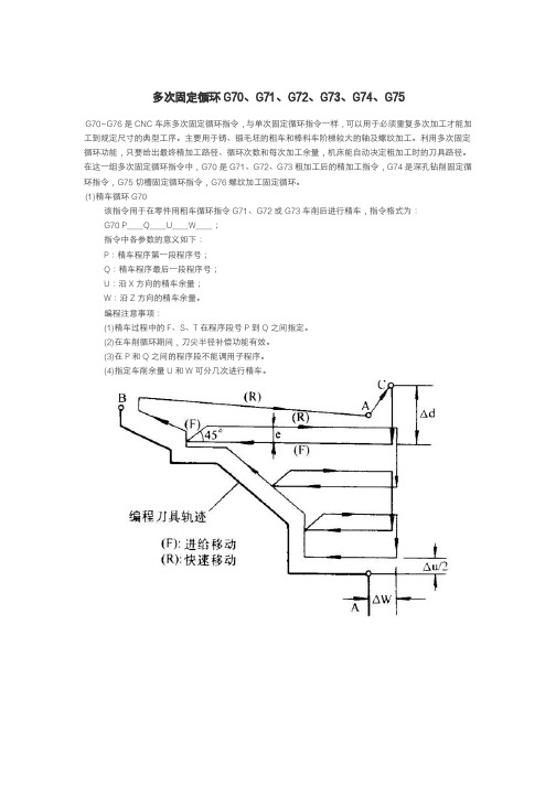
多次固定循环G70、G71、G72、G73、G74、G75G70~G76是C N C车床多次固定循环指令,与单次固定循环指令一样,可以用于必须重复多次加工才能加工到规定尺寸的典型工序。
主要用于铸、锻毛坯的粗车和棒料车阶梯较大的轴及螺纹加工。
利用多次固定循环功能,只要给出最终精加工路径、循环次数和每次加工余量,机床能自动决定粗加工时的刀具路径。
在这一组多次固定循环指令中,G70是G71、G72、G73粗加工后的精加工指令,G74是深孔钻削固定循环指令,G75切槽固定循环指令,G76螺纹加工固定循环。
(1)精车循环G70该指令用于在零件用粗车循环指令G71、G72或G73车削后进行精车,指令格式为:G70P____Q____U____W____;指令中各参数的意义如下:P:精车程序第一段程序号;Q:精车程序最后一段程序号;U:沿X方向的精车余量;W:沿Z方向的精车余量。
编程注意事项:(1)精车过程中的F、S、T在程序段号P到Q之间指定。
(2)在车削循环期间,刀尖半径补偿功能有效。
(3)在P和Q之间的程序段不能调用子程序。
(4)指定车削余量U和W可分几次进行精车。
(2)外圆/内孔粗车循环G71该指令适用于毛坯料的粗车外径与粗车内径。
如图a所示为粗车外径的加工路径,图中C是粗加工循环的起点,A是毛坯外径与端面的交点,B时加工终点。
该指令的执行过程如图a所示,其指令格式为:G71U(Δd)R(e);G71P____Q____U(Δu)W(Δw)F____S____T____;N(P)………… 用程序段号P到Q之间的程序段定义A→A΄→B之间的移动轨迹N(Q)……指令中各参数的意义如下:Δd:车削深度,无符号。
车削方向取决于方向A A΄。
该参数为模态值。
E:退刀量,该参数为模态值。
P:精车削程序第一段程序号。
Q:精车削程序最后一段程序号。
Δu: X方向精车预留量的距离和方向。
Δw: Z方向精车预留量的距离和方向。
GV_SG_473CN_CN_1035-1

微调设定值
使用 [] 和 [] 箭头按钮来微调设定值。
DATUM
增加设定值
SET 1 2
MODE 减少设定值
项目
设定值 微调
设定范围 -199 至 999
基准面(DATUM)校准
在 2 点校准过程中 , 当不能正确执行比较器输出时(由于工件表面颤 振等问题)使用 DATUM 校准。
最大灵敏度设定(操作模式 :F-1,A-1,A-2)
1 当在指定位置没有工件时,按下 [SET(] 设定)按钮并 保持至少三秒钟。
2 当“SEt”开始闪烁时,松开 [SET(] 设定)按钮。
这就结束了 2 点校准而且传感器回到检测状态。
全自动校准(操作模式 :F-1,A-1,A-2)
当目标物正在移动时,用此方法执行校准。
设定值(绿色) 当前值(红色)
DATUM
SET 1 2
MODE
频道号指示灯
设定值 / 当前值显示 按 [MODE(] 模式)按钮切换 频道(频道号指示灯)。DAΒιβλιοθήκη UMSET 1 2 DATUM
交替
MODE
SET 1 2
MODE
或 峰值(绿色) 谷值(红色)
峰值 / 谷值显示 按 [ ] 箭头按钮重设峰值和谷值。
当前值变为“0”, 零点位置设定完成。
当设定了切换目标值,执行了零点位置设定后不会使当前值变为“0”。
᎙!ሃ
而是当前值变为切换目标值。
ૣ!د同时按下 [] 和 [] 箭头按钮至少三秒钟取消零点(切换目标值)。
键锁
设定 / 释放键锁 当在主屏幕上按下 [MODE(] 模式)按钮,按下并保持 [] 或 [] 按钮至少三秒钟。 这时候设定(或释放)键锁并将传感器返回到主屏幕。
473贴片电阻-概述说明以及解释

473贴片电阻-概述说明以及解释1.引言1.1 概述贴片电阻是一种常用的电子元件,广泛应用于电路板和电子设备中。
它是一种小型、方便安装和焊接的表面贴装电阻,具有较高的稳定性和精确的阻值。
相比传统的插件电阻,贴片电阻具有体积小、重量轻、可靠性高等优点。
贴片电阻的工作原理很简单,它通过电阻材料的阻值来限制电流的流动。
当电流通过贴片电阻时,会产生与电阻值成正比的电压降。
在电子电路中,贴片电阻常用于调节、分压、限流等功能。
在电子行业中,贴片电阻有着广泛的种类和规格。
根据其尺寸不同,常见的贴片电阻尺寸有0603、0805、1206等。
这些数字代表了电阻的长宽尺寸,比如0603表示长度为0.06英寸、宽度为0.03英寸。
此外,贴片电阻还有不同的阻值范围可供选择,从几欧姆到几兆欧姆都有。
贴片电阻在各个领域都有广泛的应用。
在通信领域,贴片电阻常用于通信设备和无线电设备中,起到信号传输和干扰抑制的作用。
在消费电子产品中,贴片电阻被广泛应用于手机、电视、音响等电子设备中,保证设备的正常运行和高品质音视频效果。
此外,贴片电阻还用于计算机、医疗器械、汽车电子等行业,为各种电子设备提供稳定的电阻功能。
综上所述,贴片电阻作为一种重要的电子元件,具有小巧、稳定、精确的特点,广泛应用于通信、消费电子、计算机等领域。
随着电子技术的不断发展,贴片电阻将继续发挥重要作用,并在尺寸、功耗、阻值范围等方面不断创新和改进。
因此,对于工程师和电子爱好者而言,深入了解和掌握贴片电阻的相关知识是非常有必要的。
1.2文章结构文章结构部分内容可以如下编写:文章结构:本文将围绕着473贴片电阻展开讨论,文章主要分为引言、正文和结论三大部分。
引言部分将首先对贴片电阻进行概述,介绍其定义、原理和应用领域等基本信息,为读者提供一个整体的认识和理解基础。
接着,文章将详细介绍本文的结构,即各个章节的内容安排和主要讨论的点,以便读者可以清楚地了解文章的组织结构和主旨。
Jz4730_datasheet

Ingenic® Jz4730 ProcessorData SheetConfidential® Ingenic Semiconductor Co.LimitedPackaging and Pinout InformationContentsCHAPTER 1PRODUCT OVERVIEW (1)1.1P ROCESSOR B LOCK D IAGRAM (1)1.2P ROCESSOR F EATURES (2)1.2.1JzRISC Core (2)1.2.2System Control and Timers (2)1.2.3Memory Interface (2)1.2.4Inter-chip Connectivity (3)1.2.5Connectivity and Expansion (3)1.2.6Multimedia Interface (4)1.2.7Clock and Power Management (4)CHAPTER 2PACKAGING AND PINOUT INFORMATION (5)2.1O VERVIEW (5)2.2P IN D ESCRIPTION (6)2.3P ACKAGE D IMENSION (16)2.4B ALL A SSIGNMENT (17)2.5P ACKAGE P OWER R ATINGS (19)CHAPTER 3ELECTRICAL SPECIFICATIONS (20)3.1A BSOLUTE M AXIMUM R ATINGS (20)3.2P OWER C ONSUMPTION S PECIFICATIONS (20)3.3O PERATING C ONDITIONS (22)3.4DC S PECIFICATIONS (22)3.5AC S PECIFICATIONS (24)3.6O SCILLATOR E LECTRICAL S PECIFICATIONS (24)3.6.132.768KHz Oscillator Specifications (24)3.6.2 3.6864MHz Oscillator Specifications (24)3.7R ESET AND P OWER AC T IMING S PECIFICATIONS (24)3.7.1Power-On Timing (25)3.7.2Hardware Reset Timing (26)3.8M EMORY B US AND PCMCIA AC S PECIFICATIONS (26)3.9P ERIPHERAL M ODULE AC S PECIFICATIONS (27)3.9.1LCD Module Timing (27)3.9.2CIM Module Timing (27)3.9.3SPI Module Timing (27)3.9.4External DMA Request and Grant (27)Jz4730 Processor Data Sheet ConfidentialPackaging and Pinout InformationChapter 1 Product OverviewThe Jz4730 processor is the competitive product of application processor, which meet thedemand of the portable handheld market. Incorporate the JzRISC core based on leadingmicroarchitecture technology, this processor provides high integration, high performance andlow power consumption solution for embedded device.The JzRISC is the advanced and power-efficient 32-bit RISC core with 16K I-Cache and 16KD-Cache in this processor, operating at speeds up to 400MHz. On-chip modules such as LCDcontroller, AC97/I2S controller and camera interface offer designers a rich suite of peripheralsfor multimedia application. The memory interface supports a variety of memory types that allow flexible design requirements, include the glueless connection to NAND Flash for cost sensitiveapplications. WLAN, Bluetooth and expansion options are provided through the PCMCIA/CF,USB, and MMC/SD host controllers. And the other peripherals such as UART, SPI, andEthernet controller as well as general-system resources provide enough compute andconnectivity capability for many applications. For the processor block diagram, refer to .1.1 Processor Block Diagram1Packaging and Pinout InformationFeatures1.2 Processor1.2.1 JzRISC CoreJzRISC core is a high performance and low power microprocessor core.•32-bit RISC CPU, clock up to 400MHz•Low power consumption – <0.5mW/MHz•16K I-Cache + 16K D-Cache•MMU support with I-TLB, D-TLB and J-TLB•Hardware Debug support via JTAG port1.2.2 System Control and Timers• Interrupt controller―Total 28 maskable interrupt sources from on-chip peripherals and external request through GPIO ports―Interrupt source and pending registers for software handling―Unmasked interrupts can wake up the chip in sleep or standby mode • Operating system timer―Provide three separate channels―32-bit counter with auto-reload function―Generate interrupt when the down counter underflows―Six counting clock sources: RTCCLK (real time clock), EXTAL (external clock input), φ/4, φ/16, φ/64 and φ/256. (φ is the internal clock for on-chip peripheral) • Watchdog timer―32-bit counter with RTC clock―Generate power-on reset•Pulse Width Modulator (PWM)―Period control through a 6-bit clock divider and a 10-bit period counter―10-bit pulse counter•General-Purpose I/O ports―Total GPIO pin number is 128―Each pin can be configured as general-purpose input or output or multiplexed with internal chip functions―Each pin can act as a interrupt source and has configurable rising/falling edge or high/low level detect manner, and can be masked independently―Each pin can be configured as open-drain when output1.2.3 Memory Interface•Static memory interface―Direct interface to SRAM, ROM, Burst ROM, and NOR Flash―Six chip-select pin for static memory, each can be configured separately―Support 8, 16 or 32 bits data width―The size and base address of static memory banks are programmable •NAND Flash interface―Support on CS3, sharing with static memory bank 3―Support all 8-bit/16-bit NAND Flash devices regardless of density and organization―Hardware ECC generation―Support automatic boot up from NAND Flash devices• Synchronous DRAM Interface― 2 banks with programmable size and base address―32-bit and 16-bit data bus width is supported―Multiplexes row/column addresses according to SDRAM capacity―Two-bank or four-bank SDRAM is supported2Packaging and Pinout Information ―Supports auto-refresh and self-refresh functions―Supports power-down mode to minimize the power consumption of SDRAM―Supports page mode•PC Card Interface―Fully compliant with the release of March 1997 of PC Card standard (16-bit PC Card)―DMA transfer support―Supports two PCMCIA or CF socket•Direct Memory Access Controller―Eight independent DMA channels―Transfer data units: 8-bit, 16-bit, 32-bit, 16-byte or 32-byte―Transfer requests can be: auto-request within DMA; on-chip peripheral module request;and external request―Interrupt on transfer completion or transfer error―Supports two transfer modes: single mode or block mode•The Jz4730 processor system supports little endian only1.2.4 Inter-chip Connectivity•I2C bus interface―Only supports single master mode―Supports I2C standard-mode and F/S-mode up to 400 kHz―Double-buffered for receiver and transmitter―Supports general call address and START byte format after START condition • Synchronous serial interface―Supports three formats: TI’s SSP, National Microwire, and Motorola’s SPI―Configurable 2 - 17 (or multiples of them) bits data transfer― Full-duplex/transmit-only/receive-only operation―Supports normal transfer mode or Interval transfer mode―Programmable transfer order: MSB first or LSB first―17-bit width, 16-level deep transmit-FIFO and receive-FIFO―Programmable divider/prescaler for SSI clock―Back-to-back character transmission/reception mode1.2.5 Connectivity and Expansion• Four UART interface―5, 6, 7 or 8 data bit operation with 1 or 1.5 or 2 stop bits, programmable parity (even, odd, or none)―16x8bit FIFO for transmit and 16x11bit FIFO for receive data―Programmable baud rate up to 230.4Kbps―Interrupt support for transmit, receive (data ready or timeout), and line status―Supports DMA transfer mode―Provide complete serial port signal for modem control functions―Support slow infrared asynchronous interface (IrDA)•Two smart card controller―Compliant with ISO/IEC standard 7816-3, supports both normal smart card and UIM card interface―Support asynchronous character (T = 0)/ block (T = 1) communication modes―8-bit, 16-level FIFO, and programmable SCC_CLK output clock frequency―Interrupt support for data communication and error handling•USB host interface―Open Host Controller Interface (OHCI)-compatible and USB Revision 1.1-compatible •USB device interface―Compliant with USB protocol revision 1.1―Supports suspend/resume and remote wakeup―Supports 8 physical endpoints and 9 logic endpoints3Packaging and Pinout Information―Supports bulk, isochronous, interrupt and control transaction•Ethernet MAC interface―Compliant with IEEE802.3, 802.3u―10/100 Mbps data transfer rates with full and half duplex modes―IEEE802.3 compliant MII interface to talk to an external PHY― VLAN support―2K bytes Tx buffers, and 2K bytes Rx buffers―Supports DMA engine using burst mode―Supports remote wake-up frame and magic packet frame1.2.6 Multimedia Interface• LCD―Single-panel display in active mode, and single- or dual-panel displays in passive mode―Up to 64K colors in active mode, and up to 4096 colors in passive mode―Display size up to 800×600 pixels― 256×16 bits internal palette RAM―Support ITU601/656 data format• AC97/I2S controller―Supports 16, 18 and 20 bit sample for AC-link format, and 8, 16, 18, 20 and 24 bit for I2S/MSB-Justified format―DMA transfer mode support―Programmable Output channels and Input channels or Fixed mode for AC-link format―Power down mode and two wake-up mode support for AC-link format―Programmable Interrupt function support• Camera interface―Input image size up to 2048×2048 pixels―Supports CCIR656 data format―32×32 image data receive FIFO with DMA support•MultiMedia Card/Secure Digital Controller―Compliant with “The MultiMediaCard System Specification version 3.3”―Compliant with “SD Memory Card Specification version 1.01” and “SDIO Card Specification version 1.0” with 1 command channel and 4 data channels―20~80 Mbps maximum data rate―Supports up to 10 cards (including one SD card)―Maskable hardware interrupt for SD I/O interrupt, internal status, and FIFO status1.2.7 Clock and Power Management•Clock generation Module―On-chip 3.6864MHz oscillator circuit―One On-chip phase-locked loops (PLL) with programmable multiple-ratio. Internal counter are used to ensure PLL stabilize time―PLL on/off is programmable by software―ICLK, PCLK, SCLK, MCLK and LCLK frequency can be changed separately for software by setting division ratio• Power Manager―support six low-power modes and function: NORMAL mode; DOZE mode; IDLE mode;SLEEP mode; HIBERNATE mode; and MODULE-STOP function.4Packaging and Pinout InformationChapter 2 Packaging and Pinout Information2.1 OverviewJz4730 processor is packaged in a 256-pin ball grid array (LFBGA), has a square 17x17 and 4 rowsball assignment. The following figures and tables list all the functional pins.Most of the GPIO pins are multiplexed on the on-chip peripheral modules, and the reset state isgeneral-purpose input with internal pull-up or pull-down.5Packaging and Pinout InformationDescription2.2 PinFigure 2-1 Jz4730 Pin Diagram (1) 6Figure 2-2 Jz4730 Pin Diagram (2)Table 2-1 EMC Pins (81 for 256; 9 GPIO)Pin Name Type DescriptionComments D[31:16] I/O Memory data bus, used for 32-bit memories D[15:0] I/O Memory data bus, lower 16 bits of the data bus A[25:17]OutputStatic memory addressA[16:2] OutputSDRAM memory address, multiplexing staticmemory addressA[1:0] Output Static memory address DCS0_ Output SDRAM chip select 0DCS1 / GP82 I/OSDRAM chip select 1 /GPIO 82 Pull-up input at reset RAS_ Output Row address strobe for SDRAM CAS_ Output Column address strobe for SDRAM CKE Output Clock enable for SDRAM RDWR_ Output Read/write signal, 1 – read; 0 – writeCKO Output SDRAM clock CS0_ Output Static memory bank 0 chip selectCS1_ /GP83I/OStatic memory bank 1 chip select / GPIO 83 Pull-up input at resetCS2_ / GP84 I/OStatic memory bank 2 chip select /GPIO 84 Pull-up input at resetCS3_ / GP85 I/OStatic memory bank 3 chip select /GPIO 85 Pull-up input at resetCS4_ / GP86 I/OStatic memory bank 4 chip select /GPIO 86 Pull-up input at resetCS5_ / GP87 I/OStatic memory bank 5 chip select /GPIO 87 Pull-up input at reset RD_ / POE_ OutputRead strobe for static memory device /Pcmcia memory read strobeWE_ /PWE_OutputWrite strobe for static memory device / Pcmcia memory write strobe WE0_ / PIOW_ OutputByte 0 write enable /pcmcia IO write strobe WE1_ / PIOR_ OutputByte 1 write enable /pcmcia IO read strobe WE2_ / PREG_ OutputByte 2 write enable /pcmcia register selectWE3_ Output Byte 3 write enableWAIT_ / PWAIT_ InputWait signal for slow memory /pcmcia wait inputInternal pull-up FRE_ /GP79I/ORead enable for NAND Flash / GPIO 79 Pull-up input at resetFWE_ /GP80I/OWrite enable for NAND Flash / GPIO 80 Pull-up input at resetFRB_ /GP81 I/OReady or busy signal for NAND Flash / GPIO 81 Pull-up input at resetTable 2-2 PCMCIA/CF Pins (6 for 256; 6 GPIO)Pin Name Type Description Comments IOIS16_ /GP92 / TP[3] I/OPCMCIA IO address 16 bit select /GPIO 92 /Test port [3]Pull-up input atresetPSKTSEL /GP91 / TP[2] I/OPCMCIA socket select /GPIO 91 /Test port [2]Pull-up input atresetPCE1_ /GP90 / TP[1] I/OPCMCIA card enable 1 /GPIO 90 /Test port [1]Pull-up input atresetPCE2_ /GP93 / TP[0] I/OPCMCIA card enable 2 /GPIO 93 /Test port [0]Pull-up input atresetINPACK_ / GP88 I/OPCMCIA INPACK_ input /GPIO 88Pull-up input atresetPBVD2 / GP89 I/OPCMCIA BVD2 input /GPIO89Pull-up input atreset Table 2-3 LCD Pins (24 for 256; 24 GPIO)Pin Name Type Description Comments LCD_D[15:8] /GP55 ~ GP48 / TP[17:10] I/OHigher 8-bit of LCD data /GPIO 55 ~ GPIO 48 /Test port [17:10]Pull-downinput at resetLCD_D[7:0] / GP47 ~ GP40 I/OLower 8-bit of LCD data /GPIO 47 ~ GPIO 40Pull-up input atresetLCD_VSYNC / GP56 I/OLCD frame clock/vertical sync /GPIO 56Pull-downinput at resetLCD_HSYNC / GP57 I/OLCD line clock/horizonal sync /GPIO 57Pull-up input atresetLCD_PCLK / GP58 I/OLCD pixel clock /GPIO 58Pull-downinput at resetLCD_DE / GP59 I/OSTN AC bias drive/Non-STN data enable output /GPIO 59Pull-downinput at resetLCD_SPL / GP60 I/OLCD SPL output for special TFT panel /GPIO 60Pull-up input atresetLCD_CLS / GP61 I/OLCD CLS output for special TFT panel /GPIO 61Pull-up input atresetLCD_PS / GP62 I/OLCD PS output for special TFT panel /GPIO 62Pull-up input atresetLCD_REV / GP63 I/OLCD REV output for special TFT panel /GPIO 63Pull-up input atresetTable 2-4 I2C Pins (2 for 256)Pin Name Type Description Comments I2C_SDA I/O I2C serial data Open drain I2C_SCK I/O I2C serial clock Open drainTable 2-5 SCC Pins (4 for 256; 4 GPIO)Pin Name Type Description CommentsSCC0_DATA / GP64 I/OSCC0 data /GPIO 64Pull-up input atresetSCC0_CLK / GP66 I/OSCC0 clock /GPIO 66Pull-up input atresetSCC1_DATA / GP65 I/OSCC1 data /GPIO 65Pull-up input atresetSCC1_CLK / GP67 I/OSCC1 clock /GPIO 67Pull-up input atreset Table 2-6 UART3 Pins (4 for 256; 8 GPIO)Pin Name Type Description CommentsUART3_CTS_ / GP17 I/OUART3 clear to send /GPIO 17Pull-up input atresetUART3_RTS_ /GP23 / TP[8] I/OUART3 request to send /GPIO 23 /Test port [8]Pull-up input atresetUART3_TxD_ / GP21 I/OUART3 TxD /GPIO 21Pull-up input atresetUART3_RxD_ / GP16 I/OUART3 RxD /GPIO 16Pull-up input atreset Table 2-7 UART2 Pins (2 for 256; 2 GPIO)Pin Name Type Description CommentsUART2_TxD_ / GP125 I/OUART2 TxD /GPIO 125Pull-up input atresetUART2_RxD_ / GP111 I/OUART2 RxD /GPIO 111Pull-up input atreset Table 2-8 UART1 Pins (2 for 256; 2 GPIO)Pin Name Type Description CommentsUART1_TxD_ / GP25 I/OUART1 TxD /GPIO 25Pull-up input atresetUART1_RxD_ / GP24 I/OUART1 RxD /GPIO 24Pull-up input atresetTable 2-9 UART0 Pins (2 for 256; 2 GPIO)Pin Name Type Description CommentsUART0_TxD_ / GP127 I/OUART0 TxD /GPIO 127Pull-up input atresetUART0_RxD_ / GP126 I/OUART0 RxD /GPIO 126Pull-up input atreset Table 2-10 SSI Pins (5 for 256; 5 GPIO)Pin Name Type Description CommentsSSI_CLK / GP72 I/OSSI clock output /GPIO 72Pull-up input atresetSSI_CE1_ / GP73 I/OSSI chip enable 1 /GPIO 73Pull-up input atresetSSI_DT / GP74 I/OSSI data output /GPIO 74Pull-up input atresetSSI_DR / GP75 I/OSSI data input /GPIO 75Pull-up input atresetSSI_CE2_ /SPI_GPC / GP76 /TP[9] I/OSSI chip enable 2 /SSI GPC /GPIO 76 /Test port [9]Pull-up input atreset Table 2-11 DMA Pins (4 for 256; 6 GPIO)Pin Name Type Description CommentsDREQ0 / GP12IODMA external request 0 /GPIO 12Pull-up input atresetDACK0 / GP13 IODMA transfer acknowledge 0 /GPIO 13Pull-up input atresetAEN /GP26 / TP[5] IOAddress enable for transfer /GPIO 26 /Test port [5]Pull-up input atresetEOP /GP27 / TP[6] IODMA transfer end /GPIO 27 /Test port [6]Pull-up input atreset Table 2-12 PWM Pins (2 for 256; 2 GPIO)Pin Name Type Description CommentsPWM0 / GP94 I/OPWM 0 output /GPIO 94Pull-up input atresetPWM1 / GP95 I/OPWM 1 output /GPIO 95Pull-up input atresetTable 2-13 UHC Pins (7 for 256; 4 GPIO)Pin Name Type Description CommentsUSB_CLK / GP28 I/OUSB 48MHz clock /GPIO 28Pull-up input atresetDPLS0 AnalogI/OUSB transceiver data plus 0DMNS0 AnalogI/OUSB transceiver data minus 0OVC0 / TEST_SEN IOvercurrent input 0 /Scan enable for scan-reqPPWR0 / GP29 I/OPower enable output 0 /GPIO 29Pull-up input atresetDPLS1 AnalogI/OUSB transceiver data plus 1DMNS1 AnalogI/OUSB transceiver data minus 1Table 2-14 MAC Pins (17 for 256; 13 GPIO)Pin Name Type Description CommentsMII_COL / GP115 I/OEthernet collision /GPIO 115Pull-up input atresetMII_CRS / GP116 I/OEthernet carrier sense /GPIO 116Pull-up input atresetMII_TX_CLK Input Ethernet transmit clockMII_TXD[3] / GP120 I/OEthernet transmit data /GPIO 120Pull-up input atresetMII_TXD[2] / GP119 I/OEthernet transmit data /GPIO 119Pull-up input atresetMII_TXD[1] / GP118 I/OEthernet transmit data /GPIO 118Pull-up input atresetMII_TXD[0] / GP117 I/OEthernet transmit data /GPIO 117Pull-up input atresetMII_TX_EN / GP112 I/OEthernet transmit enable /GPIO 112Pull-up input atresetMII_RX_CLK Input Ethernet receive clockMII_RX_DV / GP113 I/OEthernet receive data valid /GPIO 113Pull-up input atresetMII_RXD[3] / GP124 I/OEthernet receive data /GPIO 124Pull-up input atresetMII_RXD[2] / GP123 I/OEthernet receive data /GPIO 123Pull-up input atresetMII_RXD[1] / GP122 I/OEthernet receive data /GPIO 122Pull-up input atresetMII_RXD[0] / GP121 I/OEthernet receive data /GPIO 121Pull-up input atresetMII_RX_ER / GP114 I/OEthernet receive error /GPIO 114Pull-up input atresetMII_MDC Output Ethernet management clockMII_MDIO I/O Ethernet management data inoutTable 2-15 CIM Pins (12 for 256; 12 GPIO)Pin Name Type Description CommentsCIM_D [7:0] / GP7 ~ GP0 I/OData input from image sensor /GPIO 7 ~ GPIO 4Pull-up input atresetCIM_PCLK / GP10 I/OCIM pixel clock /GPIO 10Pull-up input atresetCIM_MCLK /GP11 / TP[4] I/OCIM master clock /GPIO 11 /Test port [4]Pull-up input atresetCIM_HSYNC / GP9 I/OCIM horizontal clock /GPIO 9Pull-up input atresetCIM_VSYNC / GP8 I/OCIM vertical clock /GPIO 8Pull-up input atreset Table 2-16 PS2 Keyboard Pins (2 for 256; 2 GPIO)Pin Name Type Description CommentsPS2_KCLK / GP32 I/OPS/2 keyboard clock /GPIO 32Pull-up input atresetPS2_KDATA / GP33 I/OPS/2 keyboard data /GPIO 33Pull-up input atreset Table 2-17 AC97/I2S Pins (6 for 256; 6 GPIO)Pin Name Type Description CommentsBITCLK / GP77 I/OAIC serial clock pin /GPIO 77Pull-up input atresetSDATA_IN / GP71 I/OAIC serial data input /GPIO 71Pull-up input atresetSDATA_OUT / GP70 I/OAIC serial data output /GPIO 70Pull-up input atresetSYNC / GP78 I/OAIC frame synchronization pin /GPIO 78Pull-up input atresetSYSCLK / GP68 I/OAIC system clock output /GPIO 68Pull-up input atresetACRESET_ / GP69 I/OAIC reset output /GPIO 69Pull-up input atresetTable 2-18 MSC Pins (6 for 256; 6 GPIO)Pin Name Type Description CommentsMSC_DAT[3] / GP37 I/OMSC data /GPIO 37Pull-up input atresetMSC_DAT[2] / GP36 I/OMSC data /GPIO 36Pull-up input atresetMSC_DAT[1] / GP35 I/OMSC data /GPIO 35Pull-up input atresetMSC_DAT[0] / GP34 I/OMSC data /GPIO 34Pull-up input atresetMSC_CMD / GP38 I/OMSC command /GPIO 38Pull-up input atresetMSC_CLK / GP39 I/OMSC clock output /GPIO 39Pull-up input atresetTable 2-19 GPIO Pins (15 for 256;)Pin Name Type Description CommentsGP110 ~ GP96 I/O Special GPIO 110 ~ GPIO 96 Pull-up input at resetTable 2-20 JTAG Pins (5 for 256)Pin Name Type Description CommentsTRSTN_ InputJTAGreset Internal pull-downTMS Input JTAG mode select Internal pull-up TDI Input JTAG serial data input Internal pull-upTCK InputJTAGclock Internal pull-downTDO Output JTAG serial data outputTable 2-21 System Pins (11 for 256)Pin NameType Description Comments EXTALAnalogInput System clock input XTAL AnalogOutputOSC outputRTCCLK Input RTC clock inputRESETOUT_ Output Reset output RESETP_ Input System power on reset inputBOOT_SEL[3] Input Boot select input 3:0->boot from ROM at CS0;1->boot from NAND flash device at CS3 Internal pull-down BOOT_SEL[2] InputBoot select input 2:NAND flash address cycles when boot from it,0->low cycle; 1->high cycleInternal pull-down BOOT_SEL[1] InputBoot_select input 1:NAND flash page size when boot from it,0->512B; 1->2048BInternal pull-down BOOT_SEL[0] InputBoot select input 0:NAND flash width when boot from it,0->8bit; 1->16bit Internal pull-down TEST_MODEInputChip test modeInternal pull-downTAP_MD InputTAP mode input- (1: internal JTAG; 0: boundary) Internal pull-downTable 2-22 Power Pins (28 for 256)Pin Name DescriptionVDD(IO1) Power supply for IO pad (1.8v) VSS(IO1) Ground supply for IO pad (0v) VDD(IO2) Power supply for IO pad (3.3v) VSS(IO2) Ground supply for IO pad (0v) VDD(core) Power supply for core (1.8v) VSS(core) Ground supply for core (0v)VDD(PLL) PLL power supply for analog (1.8v) VSS(PLL) PLL ground supply for analogVDD(USB) Power supply for USB IO pad (3.3v) VSS(USB) Ground supply for USB IO pad (0v)Dimension 2.3 Package2.4 BallAssignmentFigure 2-3 Jz4730 256-ball BGA Pinout (Top View)Table 2-23 Ball AssignmentBall # Signal Name Ball # Signal Name Ball #Signal NameA1 MII_TX_CLK E19 A[4] T17 NCA2 MII_MDC E20 A[5] T18 UART1_RXDA3 MII_RX_ER F1 LCD_D[6] T19 UART2_RXDA4 MII_RX_CLK F2 LCD_D[9] T20 UART1_TXDA5 AEN F3 LCD_D[11] U1 DPLS0A6 VDD(IO1) F4 MII_TXD[2] U2 DMNS0A7 CS5_ F17 A[6] U3 VSS(USB)A8 CS2_ F18 A[7] U4 NCA9 WAIT_ F19 A[8] U5 XTALTDOA[9] U6A[0] F20A10A11 A[18] G1 LCD_D[2] U7 TRSTN_A12 A[22] G2 LCD_D[4] U8 SSI_DRA13 A[25] G3 LCD_D[8] U9 VDD(IO2)A14 CKO G4 VSS(IO2) U10 VSS(IO2)A15 WE0_ G17 A[10] U11 VDD(core)A16 D[2] G18 A[11] U12 VSS(core)A17 D[6] G19 A[12] U13 GP99A18 D[9] G20 A[13] U14 GP108A19 D[11] H1 LCD_PCLK U15 MSC_CMDMSC_DAT[1]A20 D[12] H2 LCD_D[1] U16B1 MII_MDIO H3 LCD_D[5] U17 NCB2 MII_TXD1 H4 VDD(IO2) U18 UART3_TXDB3 MII_RXD2 H17 VSS(IO1) U19 UART3_RXDB4 MII_CRS H18 A[14] U20 UART0_RXDB5 DREQ0 H19 A[15] V1 VDD(USB)B6 DACK0 H20 A[16] V2 VSS(PLL)B7 FEW_ J1 LCD_VSYNC V3 NCB8 CS3_ J2 LCD_HSYNC V4 EXTALB9 CS0_ J3 LCD_D[0] V5 I2C_SCKB10 RD_ J4 LCD_D[3] V6 TCKB11 A[17] J17 VDD(IO1) V7 BOOT_SEL[2]B12 A[21] J18 D[16] V8 SSI_CE1_B13 A[24] J19 D[17] V9 SYSCLKB14 DCS0_ J20 D[18] V10 SYNCB15 RAS_ K1 LCD_CLS V11 PWM1B16 D[1] K2 LCD_SPL V12 SCC0_DATAB17 D[5] K3 LCD_DE V13 GP103B18 D[8] K4 VSS(core) V14 GP98B19 D[10] K17 VDD(core) V15 GP109B20 D[13] K18 D[19] V16 GP105MSC_DAT[3] C1 LCD_D[14] K19 D[20] V17C2 MII_TXD[0] K20 D[21] V18 UART3_RTS_C3 MII_TXD[3] L1 LCD_PS V19 NCC4 MII_RXD[0] L2 LCD_REV V20 UART2_TXDC5 MII_RX_DV L3 TAP_MD W1 VDD(PLL)C6 EOP L4 VDD(core) W2 RTCCLKC7 FRE_ L17 VSS(core) W3 RESETP_C8 CS4_ L18 D[22] W4 RESETOUT_C9 CS1_ L19 D[23] W5 TDIC10 WE_ L20 D[24] W6 BOOT_SEL[0]C11 A[1] M1 CIM_D[0] W7 BOOT_SEL[1]Table 2-24 Ball Assignment (continue)Ball # Signal Name Ball #Signal Name Ball #Signal NameC12 A[20] M2 CIM_D[1] W8 SSI_DTC13 A[23] M3 CIM_D[2] W9 SDATA_OUTC14 DCS1_ M4 CIM_D[3] W10 ACRESET_C15 CAS_ M17 D[25] W11 PS2_CLKC16 D[0] M18 D[26] W12 SCC0_CLKC17 D[4] M19 D[27] W13 SCC1_DATAC18 D[7] M20 D[28] W14 GP101C19 D[14] N1 CIM_D[4] W15 GP97C20 D[15] N2 CIM_D[5] W16 GP106D1 LCD_D[10] N3 CIM_D[6] W17 GP104MSC_DAT[0] D2 LCD_D[12] N4 CIM_D[7] W18D3 MII_TX_EN N17 D[29] W19 NCD4 MII_RXD[1] N18 D[30] W20 UART3_CTS_D5 MII_COL N19 D[31] Y1 NCD6 VSS(IO2) N20 IOIS16_ Y2 NCD7 FRB_ P1 CIM_MCLK Y3 NCD8 VDD(IO1) P2 CIM_PCLK Y4 I2C_SDAD9 VSS(IO1) P3 CIM_HSYNC Y5 TMSBOOT_SEL[3]D10 VDD(core) P4 CIM_VSYNC Y6D11 VSS(core) P17 VSS(IO2) Y7 SSI_CE2_D12 A[19] P18 PCE2_ Y8 SSI_CLKD13 VSS(IO1) P19 PCE1_ Y9 BITCLKSDATA_IND14 VDD(IO1) P20 PSKTSEL Y10D15 CKE R1 TEST_MD Y11 PWM0D16 WE1_ R2 VDD(core) Y12 PS2_DATAD17 D[3] R3 USB_CLK Y13 SCC1_CLKD18 RDWR_ R4 VSS(core) Y14 GP102D19 WE2_ R17 VDD(IO1) Y15 GP100D20 WE3_ R18 INPACK_ Y16 GP96E1 LCD_D[7] R19 PBVD2 Y17 GP110E2 LCD_D[13] R20 UART0_TXD Y18 GP107E3 LCD_D[15] T1 OVC0 Y19 MSC_CLKE4 MII_RXD[3] T2 PPWR0 Y20 MSC_DAT[2]E17 A[2] T3 DPLS1E18 A[3] T4 DMNS12.5 Package Power RatingsTable 2-24 θJA and Maximum Power RatingsProcessor θJA Max PowerJz4730 ??.? °C /w ?.??WChapter 3 Electrical Specifications3.1 AbsoluteMaximumRatingsThis section provides the absolute maximum ratings for the processors. Do not exceed theseparameters or the part may be damaged permanently. Operation at absolute maximum ratingsis not guaranteed.Table 3-1 Absolute Maximum RatingsSymbol Description MinMaxUnit T s StorageTemperature -40 125 °C VSS_O Offset Voltage between any two VSS pins -0.3 0.3 VVDD_O Offset Voltage between any of the followingpins: VDD(core), VDD(IO1), VDD(IO2)-0.3 0.3 VVDD_HV Voltage Applied to High Voltage Supplies(VDD(IO2), VDD(USB))VSS-0.3VSS+4.0 VVDD_LV Voltage Applied to Low Voltage Supplies(VDD(core), VDD(IO1), VDD(PLL))VSS-0.3VSS+2.5 VV IP1Voltage Applied to non-Supply pins VSS-0.3max of???VV IP2Voltage Applied to non-Supply pins VSS-0.3max ofVDD(IO2)+0.3VSS+4.0VV ESD Maximum ESD stress voltage, Human BodyModel; Any pin to any supply pin, eitherpolarity, or Any pin to all non-supply pinstogether, either polarity. Three stressesmaximum.2000 V3.2 Power Consumption SpecificationsPower consumption depends on the operating voltage, peripherals enabled, external switching activity, and external loading.The maximum power consumption specification is determined by all units running at theirmaximum: processor speed, voltage, and loading conditions. This method generates aconservative power consumption value; however, power supply and thermal managementdesign requires the highest possible power consumption for robust design. The Jz4730processor’s maximum power consumption is calculated using the following conditions:•All peripheral units operating at maximum frequency and size configuration•All I/O loads maximum (50pF for Memory interface, 100pF for peripherals)•Core operating at worst case power scenario (hit rates adjusted for worst power)•All voltages at maximum of rangeDo not exceed the maximum package power rating or T case temperature.。
FPGA可编程逻辑器件芯片5CGXFC7C6F23I7N中文规格书
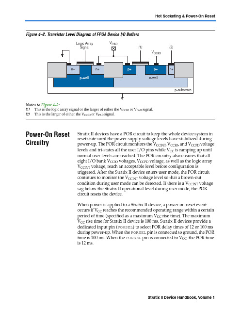
Hot Socketing & Power-On Reset Figure4–2.Transistor Level Diagram of FPGA Device I/O BuffersNotes to Figure4–2:(1)This is the logic array signal or the larger of either the V CCIO or V PAD signal.(2)This is the larger of either the V CCIO or V PAD signal.Power-On Reset Circuitry Stratix II devices have a POR circuit to keep the whole device system in reset state until the power supply voltage levels have stabilized during power-up. The POR circuit monitors the V CCINT, V CCIO, and V CCPD voltage levels and tri-states all the user I/O pins while V CC is ramping up until normal user levels are reached. The POR circuitry also ensures that all eight I/O bank V CCIO voltages, V CCPD voltage, as well as the logic array V CCINT voltage, reach an acceptable level before configuration is triggered. After the Stratix II device enters user mode, the POR circuit continues to monitor the V CCINT voltage level so that a brown-out condition during user mode can be detected. If there is a V CCINT voltage sag below the Stratix II operational level during user mode, the POR circuit resets the device.When power is applied to a Stratix II device, a power-on-reset event occurs if V CC reaches the recommended operating range within a certain period of time (specified as a maximum V CC rise time). The maximum V CC rise time for Stratix II device is 100 ms. Stratix II devices provide a dedicated input pin (PORSEL) to select POR delay times of 12 or 100 ms during power-up. When the PORSEL pin is connected to ground, the POR time is 100 ms. When the PORSEL pin is connected to V CC, the POR time is 12 ms.TriMatrix Embedded Memory Blocks in Stratix II and Stratix II GX Devices Figure2–8.Stratix II and Stratix II GX Simple Dual-Port Timing WaveformsNotes to Figure2–8:(1)The crosses in the data waveform during read mean “don’t care.”(2)The read enable rden signal is not available in M-RAM blocks. The M-RAM block in simple dual-port mode alwaysreads out the data stored at the current read address location.True Dual-Port ModeStratix II and Stratix II GX M4K and M-RAM memory blocks support thetrue dual-port mode. True dual-port mode supports any combination oftwo-port operations: two reads, two writes, or one read and one write attwo different clock frequencies. Figure2–9 shows Stratix II andStratix II GX true dual-port memory configuration.Figure2–9.Stratix II and Stratix II GX True Dual-Port Memory Note(1)Note to Figure2–9:(1)True dual-port memory supports input/output clock mode in addition to theindependent clock mode shown.TriMatrix MemoryTriMatrixMemory TriMatrix memory consists of three types of RAM blocks: M512, M4K, and M-RAM. Although these memory blocks are different, they can allimplement various types of memory with or without parity, including true dual-port, simple dual-port, and single-port RAM, ROM, and FIFO buffers. Table 2–3 shows the size and features of the different RAM blocks.Column IOEv v v Row IOE v v v vTable 2–2. Stratix II Device Routing Scheme (Part 2 of 2)Source DestinationS h a r e d A r i t h m e t i c C h a i nC a r r y C h a i n R e g i s t e r C h a i n L o c a l I n t e r c o n n e c tD i r e c t L i n k I n t e r c o n n e c t R 4 I n t e r c o n n e c t R 24 I n t e r c o n n e c t C 4 I n t e r c o n n e c t C 16 I n t e r c o n n e c t A L M M 512 R A M B l o c k M 4K R A M B l o c k M -R A M B l o c k D S P B l o c k sC o l u m n I O E R o w I O E Table 2–3.TriMatrix Memory Features (Part 1 of 2)Memory FeatureM512 RAM Block (32×18 Bits)M4K RAM Block (128×36 Bits)M-RAM Block (4K ×144Bits)Maximum performance500 MHz 550 MHz 420 MHz T rue dual-port memoryv v Simple dual-port memoryv v v Single-port memoryv v v Shift registerv v ROMv v (1)FIFO bufferv v v Pack modev v Byte enablev v v Address clock enablev v Parity bitsv v v Mixed clock modev v v Memory initialization (.mif )v v。
473QB发动机
1
发动机
F3/F3-R 轿车维修手册
十一、油底壳的安装..................................................................................................... 83 第二章 润滑系统......................................................................................................................... 86
一、机油压力报警器的检测......................................................................................... 87 二、机油压力的测试..................................................................................................... 87 三、发动机机油的更换................................................................................................. 88 四、发动机机油滤清器的更换..................................................................................... 88 五、机油滤清器螺纹连接管的更换............................................................................. 89 六、机油泵的大修......................................................................................................... 90 七、呼吸器盖板的安装................................................................................................. 93 第三章 进气歧管和排气系统..................................................................................................... 95 一、维修标准值............................................................................................................. 94 二、进气系统位置组件索引......................................................................................... 94 三、空气滤清器总成..................................................................................................... 94 四、进气歧管................................................................................................................. 94 五、排气管与消音器..................................................................................................... 94 六、检查......................................................................................................................... 94 七、进气歧管的拆卸与安装......................................................................................... 94 八、排气歧管的拆卸与安装......................................................................................... 94 第四章 发动机冷却系统............................................................................................................. 100 一、维护标准信息....................................................................................................... 101 二、冷却液................................................................................................................... 101 三、密封剂................................................................................................................... 101 四、车上维护............................................................................................................... 101 五、节温器................................................................................................................... 102 六、水泵....................................................................................................................... 103 七、进出水软管........................................................................................................... 104 八、散热器 ................................................................................................................. 105 九、调温器的检测....................................................................................................... 107 十、水泵的检测........................................................................................................... 107 十一、水泵更换........................................................................................................... 108 十二、调温器更换....................................................................................................... 108 十三、水温传感器更换............................................................................................... 109 第五章 燃油和排放系统............................................................................................................. 110 一、燃油箱................................................................................................................... 110 二、电动燃油泵........................................................................................................... 111
- 1、下载文档前请自行甄别文档内容的完整性,平台不提供额外的编辑、内容补充、找答案等附加服务。
- 2、"仅部分预览"的文档,不可在线预览部分如存在完整性等问题,可反馈申请退款(可完整预览的文档不适用该条件!)。
- 3、如文档侵犯您的权益,请联系客服反馈,我们会尽快为您处理(人工客服工作时间:9:00-18:30)。
S u b j e c t t o m o d i fi c a t i o n i n t e c h n i c a n d d e s i g n . E r r o r s a n d o m i s s i o n s e x c e p t e d .008GK473 with Profibus-DP interface FeaturesFieldbus gateway for CANopen, DeviceNet, Profibus –Operation mode status indicator by LED´s –Interface RS485 –Auto-Check functions–Technical data - electrical ratings Voltage supply 12...24 VDC Current consumption ≤200 mADisplay4 LED´s as operating status indicatorsLED operating statusDP (green) fieldbus operating statusDP (red) operating and error statusRX / TX (yellow) receiving / transmitting a token (RS485)Interfaces CANopen, DeviceNet, Profibus-DPV0Interface to SPA EIA RS485 (ASCII protocol)Data memory >10 years (flash / EEPROM)Programmable parametersAuto-Check functions Auto Scan SPAAuto Message SPA Position Auto Message SPA Error Emitted interference DIN EN 61000-6-4Interference immunityDIN EN 61000-6-2GK473Technical data - mechanical design Operating temperature -10...+50 °C Storing temperature -20...+70 °CRelative humidity 80 % non-condensing Protection DIN EN 60529IP 20E-connection D-SUB-female connector, 9-pin Plug-in screw terminals Housing type DIN rail housing EN 50022Dimensions W x H x L 22.6 x 99 x 114.5 mm Mounting DIN rail housing EN 50022Weight approx.120 gMaterialPolyamide green, UL 94V-0S u b j e c t t o m o d i fi c a t i o n i n t e c h n i c a n d d e s i g n . E r r o r s a n d o m i s s i o n s e x c e p t e d .008GK473Part number GK473.007PDFirmware2Without data carrier3Including data carrier(describing file GSD/EDS/Profibus function modules and manual)Fieldbus connection D With connector D-SUBFieldbus interface 3Profibus-DP 5CANopen 8DeviceNetInterface to SPA7RS485Auto Scan SPAIf this function is activated, during operation the gateway will proceed a continous AutoScan of all SPAs connected checking whether they are “in position”. This information can be collected by special command for fieldbus readin upon request. AutoScan spares the fieldbus master of cyclic scanning every SPA himself.Auto Message SPA PositionIf this function is activated, in the following events thegateway will automatically provide a message without prior request by the fieldbus master: After all SPAs having previ-ously been “in position” this is no longer valid for at least one SPA. The message will also be given if previously at least one SPA was not “in position” and now all SPAs are “in position” again.Auto Message SPA ErrorIf this function is activated, in the following events thegateway will automatically provide a message without prior request by the fieldbus master. After all SPAs having been previously in status “no error” (“in position” or “not in posi-tion”) now at least one SPA is in “error” status. After previ-ously at least one SPA having been in “error” status, now all SPAs are again “in position” or “not in position”.Auto-Check functionsGK473 gateway (interface converter) enables networking of approx. 32 spindle position displays (SPA) of the Baumer IVO multicon system (for example N 140, N 141, N 150 and a fieldbus-capable control (PLC). The gateway is converting the SPA’s RS485 interface into a fieldbus interface and vice-versa. Four LEDs serve as status indicators. The gateway is capable of Auto-Check functions what means a relief to the control.One bus segment allows operation of several gateways for connecting more SPAs. The gateway provides a small hous-ing for DIN rail mounting, Node-ID and bus termination can be parameterized.DescriptionS u b j e c t t o m o d i fi c a t i o n i n t e c h n i c a n d d e s i g n . E r r o r s a n d o m i s s i o n s e x c e p t e d .008GK473RS485The serial interface is conform to EIA RS485. Max. 32 multicon spindle positioning displays can be networked in any combination to RS485 bus.CANopenThe CANopen interface is in line with CAN-Bus standard ISO / DIS 11898 CAN 2.0B. Optional data transmission rates are 10 k, 20 k, 50 k, 100 k, 125 k, 250 k and 500 kBaud. The baudrate is DIP-switch settable, the user address is set by two turnable switches. The supported CANopen- communication profile is DS 301. Since there is no CANopen application profile available for this kind of gateway it is manufacturer-specific. CANopen connection is by integrated 9-pin D-SUB-connector (female). Any CAN bus loops required can be effected in the connector itself (not included in the delivery).DeviceNetDeviceNet is based on CAN Bus (Layer 2), in line with CAN-Bus standards ISO / DIS 11898 CAN 2.0B. Optionaltransmission rates of 125 kBit/s, 250 kBit/s and 500 kBit/s. The baudrate is set by DIP switch. The user address (MAC ID, 0..63) is set by help of two rotary switches. Since there Is no existing standard DeviceNet profile for this kind ofgateway it is manufacturer-specific. DeviceNet connection is by integrated 9-pin D-SUB connector (female). Any CAN bus loops required can be realized in the connector itself (not included in the delivery).ProfibusThe Profibus-DP interface is in line with Profibus standard DP-V0 (cyclic communication) according to DIN EN 50170. Optional data transmission rates are 9600, 19200, 93,75 k, 187,5 k, 500 k, 1.5 M, 3 M, 6 M and 12 MBaud. The baud rate applied is automatically recognised. Since there is no standard gateway profile available it is manufacturer-specific. Profibus-DP connection is by integrated 9-pin D-SUB connector (female). Any Profibus loops required can be realized in the connector itself (not included in the delivery).Terminal significanceConnection RS485 (plug in screw terminal)Connector Assignment Pin 1 Shield Pin 2 GND (signal)Pin 3 Data line+Pin 4 Data line-Pin 5 GND B Pin 6 UB Pin 7 GND B Pin 8UBConnection CANopen (D-SUB)Connector Assignment Pin 1 Shield / groundPin 2 CAN-Bus signal (dominant low)Pin 3 –Pin 4 –Pin 5 –Pin 6 –Pin 7 CAN-Bus signal (dominant high)Pin 8 –Pin 9–Connection DeviceNet (D-SUB)Connector Assignment Pin 1 –Pin 2 CAN-Bus signal (dominant low)Pin 3 –Pin 4 –Pin 5 –Pin 6 –Pin 7 CAN-Bus signal (dominant high)Pin 8 DRAIN Pin 9–Connection Profibus (D-SUB)Connector Assignment Pin 1 Shield / ground Pin 2 –Pin 3 Profibus B (+)Pin 4 –Pin 5 –Pin 6 –Pin 7 –Pin 8 Profibus A (-)Pin 9–Terminal assignmentS u b j e c t t o m o d i fi c a t i o n i n t e c h n i c a n d d e s i g n . E r r o r s a n d o m i s s i o n s e x c e p t e d .008GK473DimensionsProfibus function moduleFunction modules are capable of taking over basic functions in the communication between PLC and Profibus gateway what means a considerable relief to the S7 operator.Step7® provides convenient implementation of the Baumer IVO multicon project. The function modules written into AWL sub-software (FC’s) are availabe as pure text files and additionally as complete Step7® example project. This allows convenient individual modifications. The functions comprise reading and writing of current and target values into the spindle position displays (SPA), profile administrati -on and storage in the PLC, automatic address designation for the SPAs connected as well as bit parameter administra-tion. Other integrated functions enable optimized evaluation of automatic gateway scanning functions. The function modules are intended for a Siemens® S7 300DP® and available in AWL, however it can be taken for granted that by slight modifications they can be easily implemented into other AWL-capable PLCs by Siemens.Function modules。