RT423024中文资料
ST4ETA102;ST4ETA103;ST4ETA202;ST4ETB102;ST4ETA502;中文规格书,Datasheet资料
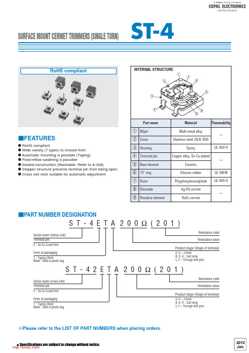
SURFACE MOUNT CERMET TRIMMERS (SINGLE TURN)● RoHS compliant● Wide variety (7 types) to choose from ● Automatic mounting is possible (Taping)● Flow/reflow soldering is possible● Sealed construction (Washable: Refer to A-328)● Stopper structure prevents terminal pin from being open.● Cross slot rotor suitable for automatic adjustmentFEATURESPART NUMBER DESIGNATIONPlease refer to the LIST OF PART NUMBERS when placing orders.S T - 4 E T A 2 0 0Ω( 2 0 1 )Series name (minus slot)Form of packagingT Taping (Reel)Blank Bulk in plastic bagTerminal pinE Sn-Cu (Lead-free)Form of packagingT Taping (Reel)Blank Bulk in plastic bagTerminal pinE Sn-Cu (Lead-free)Resistance code Resistance valueProduct shape (Shape of terminal)A, G J-hookB, D, H Gull wingC, F Through hole pinsS T - 4 2 E T A 2 0 0Ω( 2 0 1 )Series name (cross slot)Resistance code Resistance valueProduct shape (Shape of terminal)A, G J-hookB, D, H Gull wingC, F Through hole pinsST-4LIST OF PART NUMBERS Nominal resistance valuesR/R Change in total resistanceS.S. Setting stabilityMAXIMUM INPUT RATINGSRECOMMENDED P.C.B. PAD OUTLINE DIMENSIONS(Unit: mm)● ST-4EA● ST-4EG● ST-4EH● ST-4EB● ST-4EDNote) The zero point is the center of mounting.The products indicated by Amark are manufactured uponreceipt of order basis.OUTLINE DIMENSIONSUnless otherwise specified, tolerance : ±0.3 (Unit: mm)● ST -4EATop adjustment● ST● ST Top adjustmentNote the terminal position.13● ST -4EGSide adjustment● ST -4EFRear adjustment● ST -4EHSide adjustment● ST -4EDRear adjustmentNote the terminal position.Semi-standard productsSemi-standard products● ST -42ECROSS SLOT DIMENSION13OUTLINE DIMENSIONSUnless otherwise specified, tolerance : ±0.3 (Unit: mm)<Bulk pack specifications>● Unit of bulk in a plastic bag is 100 pcs. per pack.● Boxing of bulk in a plastic bag is performed with 500pcs. per box.PACKAGING SPECIFICATIONS<Taping packaging specifications>● Taping version is packaged in 500 pcs. per reel.Orders will be accepted for units of 500 pcs., i.e., 500,1000, 1500 pcs., etc.● ST-4ETA, ETB and ETD versions are boxed with 4 reels (2000 pcs.).ST-4ETG and ETH versions are boxed with one reel (500 pcs.).Maximum number of consecutive missing pieces = 2Leader length and reel dimension are shown in the dia-grams below.● EMBOSSED TAPE DIMENSIONS● REEL DIMENSIONSConforms to JIS C 0806-3In accordance with EIAJ ET-7200A(Unit: mm)● ST -4ETA/ETB/ETD● ST -4ETG/ETHHeadEndDirection of feedInstallation example Direction of feed分销商库存信息:COPAL-ELECTRONICSST4ETA102ST4ETA103ST4ETA202 ST4ETB102ST4ETA502ST4ETB101 ST4ETA203ST4ETA503ST4ETB103 ST4ETB502ST4ETB503ST4ETB202 ST4ETB203ST4ETA501ST4ETB201 ST4ETB104ST4ETA104ST4ETA105 ST4ETA204ST4ETB501ST4ETA101 ST4ETA201ST4ETA500ST4ETA504 ST4ETB204ST4ETB500ST42ETA100 ST42ETA101ST42ETA102ST42ETA103 ST42ETA104ST42ETA105ST42ETA200 ST42ETA201ST42ETA202ST42ETA203 ST42ETA204ST42ETA205ST42ETA500 ST42ETA501ST42ETA502ST42ETA503 ST42ETA504ST42ETB100ST42ETB101 ST42ETB102ST42ETB103ST42ETB104 ST42ETB105ST42ETB200ST42ETB201 ST42ETB202ST42ETB203ST42ETB204 ST42ETB205ST42ETB500ST42ETB501 ST42ETB502ST42ETB503ST42ETB504 ST4ETA205ST4ETB105ST4ETB205 ST4ETB504ST4EC101ST4EC102 ST4EC103ST4EC104ST4EC105 ST4EC201ST4EC202ST4EC203 ST4EC204ST4EC205ST4EC500 ST4EC501ST4EC502ST4EC503 ST4EC504ST4ETA100ST4ETB100 ST4EC100ST4EC200ST42EC100 ST42EC101ST42EC102ST42EC103 ST42EC104ST42EC105ST42EC200 ST42EC201ST42EC202ST42EC203 ST42EC204ST42EC205ST42EC500 ST42EC501ST42EC502ST42EC503 ST42EC504ST4ETG100ST4ETG101 ST4ETG102ST4ETG103ST4ETG104 ST4ETG105ST4ETG200ST4ETG201 ST4ETG202ST4ETG203ST4ETG204 ST4ETG205ST4ETG500ST4ETG501 ST4ETG502ST4ETG503ST4ETG504 ST4ETH100ST4ETH101ST4ETH102 ST4ETH103ST4ETH104ST4ETH105 ST4ETH200ST4ETH201ST4ETH203 ST4ETH205ST4ETH500ST4ETH501 ST4ETH502ST4ETH503ST4ETH504。
2SA2004中文资料

Collector-emitter cutoff current (Base open) Forward current transfer ratio
vi
si
VCE = −2V, IC = − 0.1 A VCE = −2 V, IC = −5 V IC = −5 A, IB = − 0.25 A IC = −5 A, IB = − 0.25 A IC = −4 A
at io n.
Max −100 −100 230 −1.2 −1.7 0.5 0.15 1.0
Unit V µA µA V V µs µs µs
Publication date: January 2003
SJD00009CED
1
This product complies with the RoHS Directive (EU 2002/95/EC).
• High forward current transfer ratio hFE • Satisfactory linearity of forward current transfer ratio hFE • Dielectric breakdown voltage of the package: > 5 kV • High−speed switching
at io n.
Request for your special attention and precautions in using the technical information and semiconductors described in this book
(1) If any of the products or technical information described in this book is to be exported or provided to non-residents, the laws and regulations of the exporting country, especially, those with regard to security export control, must be observed. (2) The technical information described in this book is intended only to show the main characteristics and application circuit examples of the products, and no license is granted under any intellectual property right or other right owned by our company or any other company. Therefore, no responsibility is assumed by our company as to the infringement upon any such right owned by any other company which may arise as a result of the use of technical information described in this book. (3) The products described in this book are intended to be used for standard applications or general electronic equipment (such as office equipment, communications equipment, measuring instruments and household appliances). Consult our sales staff in advance for information on the following applications: – Special applications (such as for airplanes, aerospace, automobiles, traffic control equipment, combustion equipment, life support systems and safety devices) in which exceptional quality and reliability are required, or if the failure or malfunction of the products may directly jeopardize life or harm the human body. – Any applications other than the standard applications intended. (4) The products and product specifications described in this book are subject to change without notice for modification and/or improvement. At the final stage of your design, purchasing, or use of the products, therefore, ask for the most up-to-date Product Standards in advance to make sure that the latest specifications satisfy your requirements. (5) When designing your equipment, comply with the range of absolute maximum rating and the guaranteed operating conditions (operating power supply voltage and operating environment etc.). Especially, please be careful not to exceed the range of absolute maximum rating on the transient state, such as power-on, power-off and mode-switching. Otherwise, we will not be liable for any defect which may arise later in your equipment. Even when the products are used within the guaranteed values, take into the consideration of incidence of break down and failure mode, possible to occur to semiconductor products. Measures on the systems such as redundant design, arresting the spread of fire or preventing glitch are recommended in order to prevent physical injury, fire, social damages, for example, by using the products. (6) Comply with the instructions for use in order to prevent breakdown and characteristics change due to external factors (ESD, EOS, thermal stress and mechanical stress) at the time of handling, mounting or at customer's process. When using products for which damp-proof packing is required, satisfy the conditions, such as shelf life and the elapsed time since first opening the packages. (7) This book may be not reprinted or reproduced whether wholly or partially, without the prior written permission of Matsushita Electric Industrial Co., Ltd.
TPS22904YFPT;中文规格书,Datasheet资料

Bump View12BALaser Marking ViewBATPS22903TPS22904 SLVS827C–FEBRUARY2009–REVISED APRIL2010 ULTRA-SMALL LOW-INPUT-VOLTAGE LOW r ON LOAD SWITCHCheck for Samples:TPS22903,TPS22904FEATURES APPLICATIONS•PDAs•Input Voltage:1.1V to3.6V•Cell Phones•Ultra-Low ON-State Resistance•GPS Devices–r ON=66mΩat V IN=3.6V•MP3Players–r ON=75mΩat V IN=2.5V•Digital Cameras–r ON=90mΩat V IN=1.8V•Peripheral Ports–r ON=135mΩat V IN=1.2V•Portable Instrumentation•500-mA Maximum Continuous Switch Current•Quiescent Current<1m A•Shutdown Current<1m A•Low Control Input Threshold Enables Use of1.2-V/1.8-V/2.5-V/3.3-V Logic•Controlled Slew Rate(5m s Max at3.6V)•Quick Output Discharge(TPS22904Only)•ESD Performance Tested Per JESD22TERMINAL ASSIGNMENTS –2000-V Human-Body ModelB GND ON(A114-B,Class II)A V OUT V IN–1000-V Charged-Device Model(C101)21•4-Terminal Wafer Chip-Scale Package(WCSP)–0.8mm×0.8mm,0.4-mm Pitch,0.5-mm HeightDESCRIPTIONThe TPS22903and TPS22904are ultra-small,low r ON single channel load switches with controlled turn on.The device contains a P-channel MOSFET that can operate over an input voltage range of1.1V to3.6V.The switch is controlled by an on/off input(ON),which is capable of interfacing directly with low-voltage control signals.In TPS22904,a85-Ωon-chip load resistor is added for output quick discharge when switch is turned off.TPS22903and TPS22904are available in a space-saving4-terminal WCSP0.4-mm pitch(YFP).The devices are characterized for operation over the free-air temperature range of–40°C to85°C.FEATURE LISTMAXIMUMr ON TYPICAL SLEW RATE QUICK OUTPUTDEVICE OUTPUT ENABLEAT3.6V AT3.6V DISCHARGE(1)CURRENTTPS2290366mΩ5m s max No500mA Active highTPS2290466mΩ5m s max Yes500mA Active high(1)This feature discharges the output of the switch to ground through a85-Ωresistor,preventing theoutput from floating.Please be aware that an important notice concerning availability,standard warranty,and use in critical applications of TexasInstruments semiconductor products and disclaimers thereto appears at the end of this data sheet.PRODUCTION DATA information is current as of publication date.Copyright©2009–2010,Texas Instruments Incorporated Products conform to specifications per the terms of the TexasONV OUTV INTPS22903TPS22904SLVS827C –FEBRUARY 2009–REVISED APRIL 2010ORDERING INFORMATION (1)T APACKAGE (2)ORDERABLE PART NUMBER TOP-SIDE MARKING (3)TPS22903YFPR ___4P_–40°C to 85°C WCSP –YFP (0.4-mm pitch)Tape and reelTPS22904YFPR___4R_(1)For the most current package and ordering information,see the Package Option Addendum at the end of this document,or see the TI web site at .(2)Package drawings,thermal data,and symbolization are available at /packaging .(3)The actual top-side marking has three preceding characters to denote year,month,and sequence code,and one following character to designate the wafer fab/assembly site.Pin 1identifier indicates solder-bump composition (1=SnPb,•=Pb-free).BLOCK DIAGRAMFigure 1.Functional Block DiagramFUNCTION TABLEONV IN TO V OUTV OUT TO GND (TPS22904ONLY)(CONTROL INPUT)L OFF ON HONOFFTERMINAL FUNCTIONSTERMINALI/O DESCRIPTIONBALL NO.NAME A1V IN I Input of the switch,bypass this input with a ceramic capacitor to ground A2V OUT O Output of the switchB1ON I Switch control input,active high,do not leave floating B2GND–Ground2Submit Documentation Feedback Copyright ©2009–2010,Texas Instruments IncorporatedTPS22903TPS22904 SLVS827C–FEBRUARY2009–REVISED APRIL2010 ABSOLUTE MAXIMUM RATINGS(1)MIN MAX UNIT V IN Input voltage range–0.34VV OUT Output voltage range V IN+0.3VV ON Input voltage range–0.34VP D Power dissipation at T A=25°C0.48WI MAX Maximum continuous switch current0.5AT A Operating free-air temperature range–4085°CT stg Storage temperature range–65150°CT lead Maximum lead temperature(10-s soldering time)300°CHuman-Body Model(HBM)2000ESD Electrostatic discharge protection VCharged Device Model(CDM)1000(1)Stresses beyond those listed under absolute maximum ratings may cause permanent damage to the device.These are stress ratingsonly,and functional operation of the device at these or any other conditions beyond those indicated under Recommended Operating Conditions is not implied.Exposure to absolute-maximum-rated conditions for extended periods may affect device reliability.THERMAL IMPEDANCE RATINGSTYP UNIT q JA Package thermal impedance(1)YFP package205°C/W (1)The package thermal impedance is calculated in accordance with JESD51-7.RECOMMENDED OPERATING CONDITIONSMIN MAX UNIT V IN Input voltage range 1.1 3.6VV OUT Output voltage range V IN VV IH High-level input voltage,ON0.85 3.6VV IL Low-level input voltage,ON0.4VC IN Input capacitor(1)1m F(1)See Application InformationCopyright©2009–2010,Texas Instruments Incorporated Submit Documentation Feedback3TPS22903TPS22904SLVS827C–FEBRUARY2009–REVISED ELECTRICAL CHARACTERISTICSV IN=1.1V to3.6V,T A=–40°C to85°C(unless otherwise noted)PARAMETER TEST CONDITIONS T A MIN TYP(1)MAX UNIT I IN Quiescent current I OUT=0,V IN=V ON Full1m AI IN(OFF)OFF-state supply current V ON=GND,OUT=Open Full1m AI IN(LEAKAGE)OFF-state switch current V ON=GND,V OUT=0Full1m A25°C6690V IN=3.6VFull9525°C7595V IN=2.5VFull11025°C90115r ON ON-state resistance I OUT=–200mA V IN=1.8V mΩFull12525°C135175V IN=1.2VFull18525°C157275V IN=1.1VFull300V IN=3.3V,V ON=0(TPS22904only),r PD Output pulldown resistance85135ΩI OUT=30mAI ON ON-state input leakage current V ON=1.1V to3.6V or GND Full1m A(1)Typical values are at V IN=3.3V and T A=25°C.SWITCHING CHARACTERISTICSV IN=3.6V,T A=–40°C to85°C(unless otherwise noted)TPS22903TPS22904 PARAMETER TEST CONDITIONSMIN TYP(1)MAX MIN TYP(1)MAX UNIT t ON Turn-ON time I OUT=100mA,C L=0.1m F0.9 1.50.9 1.5m st OFF Turn-OFF time I OUT=100mA,C L=0.1m F 5.88 5.37m st r V OUT rise time I OUT=100mA,C L=0.1m F0.8050.85m st f V OUT fall time I OUT=100mA,C L=0.1m F8.310 5.87m s (1)Typical values are at T A=25°C.4Submit Documentation Feedback Copyright©2009–2010,Texas Instruments IncorporatedInput Voltage,(V)V IN O N -S t a t e R e s i s t a n c e ,()r O NΩ0.00.10.20.30.40.50.60.70.80.91.00.70.80.9 1.0 1.1 1.2 1.3 1.4 1.5 1.6 1.7 1.8 1.9 2.0 2.1 2.2 2.3 2.4 2.5 2.6 2.7 2.8 2.9 3.0 3.1 3.2 3.3Load Current (A)V o l t a g e D r o p (m V )TPS22903TPS22904SLVS827C –FEBRUARY 2009–REVISED APRIL 2010TYPICAL CHARACTERISTICSFigure 2.r ON vs V INFigure 3.r ON vs Temperature (V IN =3.3V)Figure 4.Voltage Drop vs Load CurrentCopyright ©2009–2010,Texas Instruments Incorporated Submit Documentation Feedback 5–402585Temperature(°C)50100150200250Q u i e s c e n t C u r r e n t , I (n A )I N Input Voltage,V (V)IN Q u i e s c e n t C u r r e n t , I (n A )I N 0204060801001201401601802000.51.0 1.52.0 2.53.0 3.54.0–402585Temperature(°C)I C u r r e n t (n A )I N (O F F )2550751001251501752002252500Input Voltage,V (V)IN 0204060801001200.51.0 1.52.0 2.53.0 3.54.0I C u r r e n t (n A )I N (O F F )TPS22903TPS22904SLVS827C –FEBRUARY 2009–REVISED APRIL 2010TYPICAL CHARACTERISTICS (continued)Figure 5.Quiescent Current vs V INFigure 6.Quiescent Current vs Temperature(V ON =V IN ,I OUT =0)(V IN =3.3V,I OUT =0)Figure 7.I IN(OFF)vs V IN (V ON =0V)Figure 8.I IN(OFF)vs Temperature (V IN =3.3V)6Submit Documentation Feedback Copyright ©2009–2010,Texas Instruments IncorporatedI (L e a k a g e ) C u r r e n t (n A )IN Temperature (°C)Input Voltage,(V)V IN 1.5 2.0 2.5 3.0 3.5 4.01.00.5204060801001200I (L e a k a g e ) C u r r e n t (n A )I N –0.50.00.51.01.52.02.53.03.54.00.30.40.50.60.70.8V (V )O U T Input Voltage,V (V)ONTPS22903TPS22904SLVS827C –FEBRUARY 2009–REVISED APRIL 2010TYPICAL CHARACTERISTICS (continued)Figure 9.I IN (Leakage)vs V IN (I OUT =0)Figure 10.I IN (Leakage)vs Temperature (V IN =3.3V)Figure 11.ON-Input ThresholdCopyright ©2009–2010,Texas Instruments Incorporated Submit Documentation Feedback 7t /t (s )I r i s e f a l l m 07Temperature (°C)123456t /t (s )O N O F F m 0.06.0Temperature (°C)–40–20020406080100-40-20020406080100Temperature (°C)t f a l l (µs )-40-20020406080100Temperature (°C)t O F F (µs )TPS22903TPS22904SLVS827C –FEBRUARY 2009–REVISED APRIL 2010TYPICAL CHARACTERISTICS (continued)Figure 12.t rise (TPS22903/4)/t fall (TPS22903)vsFigure 13.t ON (TPS22903/4)/t OFF (TPS22903)vsTemperature (V IN =3.3V)Temperature (V IN =3.3V)Figure 14.t fall (TPS22904)vs Temperature (V IN =3.3V)Figure 15.t OFF (TPS22904)vs Temperature (V IN =3.3V)8Submit Documentation Feedback Copyright ©2009–2010,Texas Instruments IncorporatedI 20 mA/DIVOUTV 200 mV/DIV ON5s/DIVm I 20 mA/DIVOUTV 200 mV/DIVON20s/DIVm C = 10FI = 100 mA V = 1.2VLOUT IN mI 20 mA/DIVOUTV 200 mV/DIV ON5s/DIV m I 20 mA/DIVOUTV 200 mV/DIVON20s/DIVm C = 10FI = 100 mA V = 3.3VL OUT IN m I 20 mA/DIVOUTV 200 mV/DIVON2s/DIVm C = 0.1F I = 100 mA V = 1.2VL OUT IN m I 20 mA/DIVOUTV 200 mV/DIVON100s/DIVm C = 10FI = 100 mA V = 1.2VL OUT IN m TPS22903TPS22904SLVS827C –FEBRUARY 2009–REVISED APRIL 2010TYPICAL CHARACTERISTICS (continued)Figure 16.t ON Response Figure 17.t ON ResponseFigure 18.t ON Response Figure 19.t ON ResponseFigure 20.t OFF Response (TPS22903)Figure 21.t OFF Response (TPS22903)Copyright ©2009–2010,Texas Instruments Incorporated Submit Documentation Feedback 9I 20 mA/DIV OUTV 200 mV/DIV ON5s/DIVmI 20 mA/DIVOUTV 200 mV/DIVON200s/DIVmI 20 mA/DIVOUTV 200 mV/DIV ON5s/DIVm C = 0.1F I = 100 mA V = 3.3VL OUT IN m I 20 mA/DIVOUTV 200 mV/DIV ON2s/DIVm C = 0.1F I = 100 mA V = 1.2VL OUT IN m I 20 mA/DIVOUTV 200 mV/DIV ON100s/DIV m C = 10FI = 100 mA V = 1.2VL OUT IN m I 20 mA/DIVOUTV 200 mV/DIV ON200s/DIVm C = 10FI = 100 mA V = 3.3VL OUT IN m TPS22903TPS22904SLVS827C –FEBRUARY 2009–REVISED APRIL 2010TYPICAL CHARACTERISTICS (continued)Figure 22.t OFF Response (TPS22903)Figure 23.t OFF Response (TPS22903)Figure 24.t OFF Response (TPS22904)Figure 25.t OFF Response (TPS22904)Figure 26.t OFF Response (TPS22904)Figure 27.t OFF Response (TPS22904)10Submit Documentation Feedback Copyright ©2009–2010,Texas Instruments Incorporated分销商库存信息: TITPS22904YFPT。
RX424024中文资料

V REG.-Nr. A651, Z E214025Contact dataContact configuration 2 COContact setsingle contact Type of interruption micro disconnectionRated current8ARated voltage / max.switching voltage AC 240/400VAC Maximum breaking capacity AC2000VA Limiting making capacity, max 4 s, duty factor 10%15A Contact materialAgNi 90/106AC coil> 1 x 10⁶cycles Rated frequency of operation with / without load 6 / 600 min -1Contact ratings Type Load Cycles RX48A, 250VAC, 70°C, EN61810-14x104RX48A, 250VAC, 70°C, UL508 General purpose4x104Coil dataAC coil24...230VAC AC coiltyp 0,75VAOperative range2Coil insulation system according UL1446class FCoil versions,DC-coil Coil Rated Operate Release Coil Rated coil code voltage voltage voltage resistance powerVDC VDC VDC Ohm mW0055 3.50.550+10%5000066 4.20.668+10%529012128.4 1.2274+10%5260242416.8 2.41095+10%5260484833.6 4.84380+10%5260606042.0 6.06845+10%52611011077.011.023010+10%526All figures are given for coil without preenergization, at ambient temperature +23°CS0271-ACoil versions,AC-coil 50HzCoil Rated Operate Release Coil Rated coil code voltage voltage voltage resistance power50Hz50Hz50Hz VAC VAC VAC Ohm VA 5242418.0 3.6350+10%0.76 61511586.317.38100+15%0.76 730230172.534.532500+15%0.74 All figures are given for coil without preenergization, at ambient temperature +23°C Insulationrmsopen contact circuit1000 V rmsadjacent contact circuits2500 V rmsClearance/creepage coil-contact circuit W8 / 8 mmadjacent contact circuits W3 / 4 mmMaterial group of insulation parts W IIIaTracking index of relay base PTI 250 VInsulation to IEC 60664-1Type of insulation coil-contact circuit reinforcedopen contact circuit functionaladjacent contact circuits basicRated insulation voltage250 VPollution degree32Rated voltage system 240V400VOvervoltage category IIIOther dataRoHS - Directive 2002/95/EC compliant as per product date code 0413 Flammability class according to UL94 V-0 1)Ambient temperature range-40...+70°COperate- / release time DC coil typ 7 / 2msBounce time DC coil, NO / NC contact typ 1 / 3msVibration resistance (function) NO / NC contact20 / 4g, 10 ... 150 HzShock resistance (destruction) 100 gCategory of protection RTII - flux proof transparent version pcbMounting distance 2,5 mm 2)Resistance to soldering heat flux-proof version270°C / 10 sRelay weight14 gPackaging unit500 pcs12) Version with transparent cover: 5 mmAccessoriesFor standard version (white cover), details seeaccessories RT PCB layout / terminal assignmentBottom view on solder pinsS0163-BJDimensionsS0272-BA *) With the recommended PCB hole sizes a grid pattern from 2.5mm to 2.54mm can be used.。
Si24R1

DI
芯片开启信号,激活 RX 或 TX 模式
DI
SPI 片选信号
DI
SPI 时钟信号
DI
SPI 输入信号
DO
SPI 输出信号
DO
可屏蔽中断信号,低电平有效
Power 电源(+1.9 ~ +3.6V,DC)
Power 地(0V)
AO AI Power RF RF AI PO Power
晶体振荡器输出引脚 晶体振荡器输入引脚 给内置 PA 供电的电源输出引脚(+1.8V) 天线接口 1 天线接口 2 基准电流 内部数字电路电源,须接去耦电容 地(0V),推荐与 PCB 大面积地相连
2、引脚信息
Si24R1
VCC VSS RFN RFP VDD_PA
15
14
XI
VSS 17
9 XO
VCC 18 VDD_D 19
QFN20 4×4
8 VSS 7 VCC
VSS 20
6 IRQ
1
2
3
4
5
CE CSN SCK MOSI MISO
图 2-1 Si24R1 引脚信息图(QFN20 4×4 封装)
Preliminary
Si24R1
超低功耗高性能 2.4GHz GFSK 无线收发芯片
lm2904中文资料
lm2904中文资料LM2439 视频信号输出集成电路LM2453 视频信号输出集成电路LM2577 稳压集成电路LM2595 直流变换集成电路LM270H 自动增益及静噪控制集成电路LM2808N 伴音中频放大、鉴频及功率放大集成电路LM2904 双运算放大集成电路LM3065N 伴音中频放大、鉴频及前置放大集成电路LM3089 调频中频放大集成电路LM311N 电压比较运放集成电路LM317T 三端电源稳压1.5A集成电路LM324 四运算放大集成电路LM324M 四运算放大集成电路LM3361 解调集成电路LM33T 三端电源稳压-26V集成电路LM358 双运算放大集成电路LM358PS-T1 双运算放大集成电路LM3656 伴音中频放大、鉴频及前置放大集成电路LM377 双声道音频功率放大集成电路LM378 双声道音频功率放大集成电路LM380 场扫描输出集成电路LM381 运算放大集成电路LM382 宽带放大集成电路LM384 音频功率放大集成电路LM386 音频功率放大集成电路LM387 宽带放大集成电路LM3875T 音频功率放大集成电路LM3886 音频功率放大集成电路LM3915 发光二极管十位显示驱动集成电路LM399 基准稳压集成电路LM4500A 调频立体声解码集成电路LM4610 音调、音量、平衡调节集成电路LM4765 双声道音频功率放大30W×2集成电路LM741CN 运算放大集成电路LM79052 三端电源稳压-5.2V/1A集成电路LM8915N 显示驱动集成电路LN5241RA89 显示驱动集成电路LP62S512AX-70LLT 存储集成电路LPUVCP-96 端口功能扩展集成电路LR37632 伺服集成电路LR381641 主轴、字符控制集成电路LS0072 变音集成电路LSC4350 屏幕显示控制集成电路LSC4584P2 屏幕显示控制集成电路LT1074 开关电源稳压集成电路LT1109 升压稳压集成电路LTC1147 直流变换集成电路LTC1148 直流变换集成电路LTV1817 光电耦合集成电路LUKS-5140-M2 微处理集成电路LV1011 人工智能处理集成电路LV1100 音频信号处理集成电路LVA501 视频信号处理集成电路LVA521 制式切换集成电路M11B416256A 存储集成电路M1418VVW 微处理集成电路M2063SP 制式转换集成电路M208 系统控制集成电路M24C08 存储集成电路M24C128-WMN6 存储集成电路M27V201-200N6 中文字库集成电路M28F101AVPAD 存储集成电路M3004LAB1 红外遥控信号发射集成电路M32L1632512A 存储集成电路M34300-012SP 微处理集成电路M34300-628SP 微处理集成电路M34300M4-012SP 微处理集成电路M34300N4-011SP 微处理集成电路M34300N4-012SP 微处理集成电路M34300N4-555SP 微处理集成电路M34300N4-567SP 微处理集成电路M34300N4-584SP 微处理集成电路M34300N4-587SP 微处理集成电路M34300N4-628SP 微处理集成电路M34300N4-629SP 微处理集成电路M34300N4-657SP 微处理集成电路M34302M8-612SP 微处理集成电路M37100M8-616SP 微处理集成电路M37102M8-503SP 微处理集成电路M37103M4-750SP 微处理集成电路M37201M6 微处理集成电路M37204M8-852SP 微处理集成电路M37210M2-609SP 微处理集成电路M37210M3-010SP 微处理集成电路M37210M3-550SP 微处理集成电路M37210M3-603SP 微处理集成电路M37210M3-800SP 微处理集成电路M37210M3-901SP 微处理集成电路M37210M3-902SP 微处理集成电路M37210M4-650SP 微处理集成电路M37210M4-688微处理集成电路M37210M4-705SP 微处理集成电路M37210M4-786SP 微处理集成电路M37211M2-604SP 微处理集成电路M37211M2-609SP 微处理集成电路。
PT4243A;PT4244C;PT4242C;PT4243N;PT4244A;中文规格书,Datasheet资料
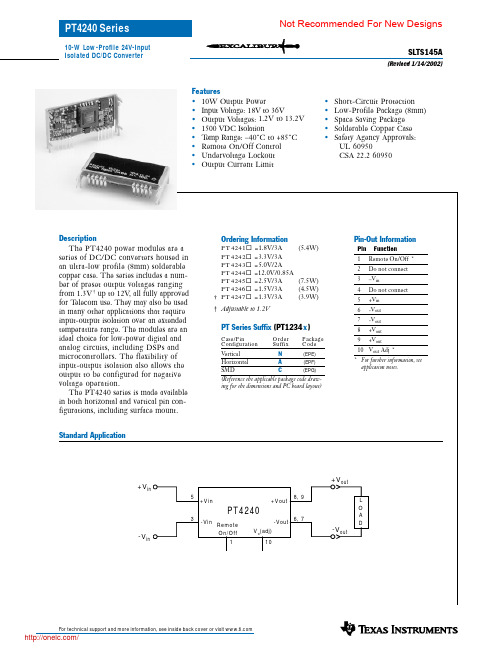
Standard Application
Ordering Information
Mechanical Shock
Mechanical Vibration
Weight Flammability
Io
Vin Vo tol Regtemp Regline Regload ∆Votot η
Vr
ttr ∆Vtr Vadj Ilim ƒs UVLO VIH VIL IIL Iin standby Cin Cout
PT Series Suffix (PT1234 x )
Case/Pin Configuration
Order Suffix
Package Code
Vertical Horizontal SMD
N
(EPE)
A
(EPF)
C
(EPG)
(Reference the applicable package code drawing for the dimensions and PC board layout)
Vo ≤ 5.0V Vo = 12V
Vo ≥2.5V
Vin =18V, ∆Vo = –1%
Over Vin range
Referenced to –Vin (pin 3)
pins 1 & 3 connected
Vo ≤ 5.0V Vo = 12V Input–output/input–case Input to output Input to output Over Vin range — Per Bellcore TR-332 50% stress, Ta =40°C, ground benign Per Mil-Std-883D, method 2002.3, 1mS, half-sine, mounted to a fixture Mil-Std-883D, Method 2007.2 20-2000Hz, all case styles soldered to PC — Materials meet UL 94V-0
PE4232中文资料
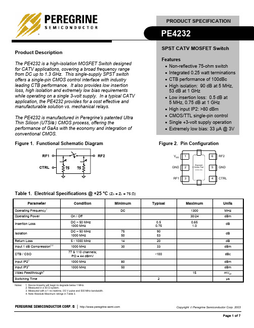
SPST CATV MOSFET Switch
Features • Non-reflective 75-ohm switch • Integrated 0.25 watt terminations • CTB performance of 100dBc • High isolation: 90 dB at 5 MHz, 53 dB at 1 GHz • Low insertion loss: 0.5 dB at 5 MHz, 0.75 dB at 1 GHz • High input IP2: >80 dBm • CMOS/TTL single-pin control • Single +3-volt supply operation • Extremely low bias: 33 µA @ 3V Figure 2. Pin Configuration
Table 3. Absolute Maximum Ratings
Symbol
VDD VI TST TOP PIN VESD
Parameter/Condition
Power supply voltage Voltage on CTRL input Storage temperature Operating temperature Input power (50Ω), CTRL=1/CTRL=0 ESD voltage (Human Body Model)
Min
-0.3 -0.3 -65 -40
Max
4.0 5.5 150 85 33/24 200
Unit
V V °C °C dBm V
Table 4. DC Electrical Specifications @ 25 °C
- 1、下载文档前请自行甄别文档内容的完整性,平台不提供额外的编辑、内容补充、找答案等附加服务。
- 2、"仅部分预览"的文档,不可在线预览部分如存在完整性等问题,可反馈申请退款(可完整预览的文档不适用该条件!)。
- 3、如文档侵犯您的权益,请联系客服反馈,我们会尽快为您处理(人工客服工作时间:9:00-18:30)。
F0149-B
V REG.-Nr. 6106, Z E214025, b14385, B C0786
Contact data
Contact configuration 2 CO or 2 NO
Contact set single contact
Type of interruption micro disconnection
Rated current8 A, UL: 10 A
Rated voltage / max.switching voltage AC 250/400VAC
Limiting continuous current UL: 10 A
Maximum breaking capacity AC 2000 VA
Limiting making capacity, max 4 s, duty factor 10%15 A
Contact material AgNi 90/10, AgNi 90/10 gold plated, AgSnO2
6
AC coil> 5 x 10⁶cycles
Rated frequency of operation with / without load 6 / 1200 min-1
Contact ratings
Type Load Cycles
RT4248A, 250VAC, NO contact, 70°C, EN61810-1100x103
RT4446(3)A, 250VAC, NO contact, 85°C; EN60730-1100x103
RT4246(2)A, 250VAC, NO/NC contact, 85°C; EN60730-1100x103
RT42410A, 250VAC, CO contact, 70°C; General purpose, UL50830x103
RT4241/2hp @ 240VAC, 1/4hp @ 120VAC, UL508
RT424Pilot duty B300, UL508
RT4248A, 30VDC, General Purpose, UL508
RT4244A, 230VAC, cosϕ=0.6, gas burner150x103
Coil data
Rated coil voltage range DC coil 5...110 VDC
AC coil24...230 VAC
Coil power DC coil typ 400 mW
AC coil typ 0,75 VA
Operative range 2
Coil insulation system according UL1446 class F
Coil versions,DC-coil
Coil Rated Operate Release Coil Rated coil
code voltage voltage voltage resistance power
VDC VDC VDC c mW
0055 3.50.562+10%403
0066 4.20.690+10%400
012128.4 1.2360+10%400
0242416.8 2.41440+10%400
0484833.6 4.85520+10%417
0606042.0 6.08570+12%420
11011077.011.028800+12%420
All figures are given for coil without preenergization, at ambient temperature +23°C
Other coil voltages on request
PCB layout / terminal assignment
Bottom view on solder pins
S0163-BJ S0163-BK
Dimensions
S0272-BA *) With the recommended PCB hole sizes a grid pattern from 2.5mm to 2.54mm can be used.
Coil versions,AC-coil 50Hz
Coil Rated Operate Release Coil Rated coil code voltage voltage voltage resistance power
50Hz50Hz50Hz VAC VAC VAC c VA 5242418.0 3.6350+10%0.76 61511586.317.38100+15%0.76 62012090.018.08800+15%0.75 700200150.030.024350+15%0.76 730230172.534.532500+15%0.74 All figures are given for coil without preenergization, at ambient temperature +23°C Insulation
rms
open contact circuit1000 V rms
adjacent contact circuits2500 V rms
Clearance / creepage coil-contact circuit W10 / 10 mm
adjacent contact circuits W3 / 4 mm
Material group of insulation parts W IIIa
Tracking index of relay base PTI 250 V
Insulation to IEC 60664-1
Type of insulation coil-contact circuit reinforced
open contact circuit functional
adjacent contact circuits basic
Rated insulation voltage250 V
Pollution degree32
Rated voltage system 240V400V
Overvoltage category III
Other data
RoHS - Directive 2002/95/EC compliant as per product date code 0413 Flammability class according to UL94 V-0
GWIT to IEC 60335-1 (IEC 60695-2-13)> 755 °C
Ambient temperature range -40...+70°C
Operate- / release time DC coil typ 7 / 2 ms
Bounce time DC coil NO / NC contact typ 1 / 3 ms
Vibration resistance (function) NO / NC contact20 / 5 g, 30 ... 300 Hz
Shock resistance (destruction) 100 g
Category of protection RTII - flux proof, RTIII - wash tight Mounting pcb or on socket
Mounting distance DC / AC coils0 / 2.5 mm
wash-tight version260°C / 5 s
Relay weight13 g
Packaging unit20 / 500 pcs
Accessories
For details see datasheet accessories RT。