PI240MC-A4中文资料
飞利浦 MCM240 使用说明

Micro Hi-Fi SystemMCM240lilIndex English------------------------------------------------6Français--------------------------------------------21Español---------------------------------------------3651目錄一般事項環保資訊 (52)隨機配件 (52)安全須知 (52)準備工作背面連接.............................................................53 – 54自選附加設備的連接 (54)將其他設備連接到本機使用遙控器之前 (54)更換遙控器電池(鋰電池 CR2025) (54)控制鍵主機和遙控器上的控制鍵 (55)基本功能開機 (56)將本機切換至待機模式 (56)省電自動待機 (56)調節音量與音效 (56)CD/MP3-CD 光碟操作裝入光碟 (57)基本的播放控制 (57)播放 MP3 光碟 (58)不同的播放模式:亂序 (SHUFFLE)和重複(REPEAT) 播放 (58)編輯光碟曲目播放清單 (58)查看曲目播放清單 (59)刪除曲目播放清單 (59)電台接收調諧選台 (60)預設電台 (60)自動預設電台手動預設電台選擇預設電台 (60)改變調諧頻階 (61)時鐘/計時器設定時鐘 (62)查看時鐘 (62)設定計時器 (62)開啟或關閉計時器(TIMER) (62)開啟或關閉關機計時器(SLEEP) (63)技術規格 (64)維護保養 (64)故障排除 (65)一般事項重要事項!請注意位於本機底部的電壓選擇器已被廠家預設為 220V。
若你的國家使用 110V-127V電壓,請在開啟本機前將電壓選擇器的電壓設定為 110V-127V。
IB-LCD240使用手册
置该动态元件。在“屏幕”中选中某个动态元件,点该栏的“删除”按钮可删除该元件。 可使用的动态元件如下: ① 数据显示 用来显示 PLC 中的某个变量(数据存储器)的值。 ② 数据设定 用来设定 PLC 中的某个变量(数据存储器)的值。 ③ 指示灯 以指示灯的形式显示 PLC 中的某个位变量(继电器)的值。 ④ 棒图 以棒图的形式显示 PLC 中的某个变量(数据存储器)的值。 ⑤ 位控文本 用 PLC 中的某个位变量(继电器)来控制所显示的文本,即该变量为 ON 时显示什 么文本,为 OFF 时显示什么文本(两者文本的长度应一致)。 ⑥ 字控文本 用 PLC 中的某个变量(数据存储器)中的值来控制所显示的文本(文本的长度应一 致)。 ⑦ 位控图片 用 PLC 中的某个位变量(继电器)来控制所显示的图片,即该变量为 ON 时显示什 么图片,为 OFF 时显示什么图片(两者图片的长度应一致)。 ⑧ 字控图片 用 PLC 中的某个变量(数据存储器)中的值来控制所显示的图片(图片的长度应一 致)。
“安理工电子”的目标:研发、生产工矿领域高端自动化产品,提供煤矿自 动化全系列解决方案,打造成煤矿行业的“西门子”,最终实现矿用电子产品生 产厂转变为自动化系统集成商。
声明
本说明书之著作权属于安徽理工大学电子设备厂。未经本公司书面同意, 不得就本手册增删、改编、改造、或仿制。 关于本手册所述之内容,本公司不负任何明示或暗示之保证或担保责任。 本手册虽然经过了仔细的检查和核对,但是仍不排除文字拼写及技术描述 错误的可能,此种错误或疏漏将于新版时予以更正。本手册的全部内容本 公司享有随时修改的权利,且不另行通知。 真诚感谢您购买和使用本公司产品,如果您在实际使用中遇到无法在本手 册中得到解答的问题,或者您对我们的产品有好的意见和建议,请您及时 与我们联系,我们会根据您的问题及时给予答复。
派克机电产品纵览说明书

■ᅠ高技术应用的控制器■ᅠ基于工业以太网的运动控制系统■ᅠ集成多轴运动控制器■ᅠ智能伺服驱动器■ᅠ工业以太网多轴伺服驱动器■ᅠ通用伺服驱动器■ᅠ智能直流调速器■ᅠ通用直流调速器派克机电产品纵览运动控制驱动技术直流调速器■ᅠ智能交流变频器■ᅠ通用交流变频器交流变频器2■ᅠ滚珠丝杠驱动工作台■ᅠ直线电机驱动工作台■ᅠ高精度微型工作台■ᅠ经济型■ᅠ高精度高精度执行器与工作台行星齿轮减速机■ᅠ伺服电机■ᅠ防爆伺服电机■ᅠ高速大功率伺服电机■ᅠ高性能车载电机■ᅠ直线电机组件■ᅠ直驱电机■ᅠ高性能伺服电机■ᅠ电动缸■ᅠ线性执行器电机执行器3ACR 系列是派克主要的独立封装的运动控制器,能够实现多达八轴的运动控制。
简单易用的项目开发组件,使应用系统构建及维护快速,高效。
ACR74C/78C 是4轴/8轴运动控制器;ACR74T 是集成4轴步进电机驱动器的驱控一体机;ACR74V/78V 是集成4轴/8轴低压伺服驱动器的驱控一体机。
强大、集成化和为机械市场设计的派克自动化运动控制器(PAC)为OEM 提供了基于标准的自动化解决方案,能够满足严苛的应用要求。
PAC 将先进逻辑、多轴运动、信号处理和网络发布的可视化整合到一个以性能为导向的解决方案中,进而消除不必要的硬件和通信链接,并提高开发者的效率。
PAC网络架构派克自动化运动控制器 - PACACR 控制器系列•ᅠ K eywords: PAC CPU 运算能力更强•ᅠP AC: EtherCAT, 多轴插补•ᅠA CR:模拟量模式,简单易用ACR7C/7V ACR7000PAC3404智能伺服驱动器 - Compax3Compax3是派克汉尼汾不同国家和地区推出的伺服驱动器产品。
驱动器系列包括单轴,多轴驱动器,还有液压控制器。
这一系列驱动的功率从1到110kVA。
这一伺服驱动器的整个研发及制造过程全部在德国完成。
另外的生产基地也在美国建成。
作为一款销往不同国家和地区的伺服驱动控制器,Compax3在世界各地都有销售。
IE-MiniMc 用户手册说明书

Advantech B+B SmartWorx - Americas707 Dayton RoadOttawa, IL 61350 USAPhone (815) 433-5100Fax (815) 433-5105Advantech B+B SmartWorx - European HeadquartersWestlink Commercial ParkOranmore, Co. Galway, IrelandPhone +353 91-792444Fax +353 91-792445B+B SMARTWORX TECHNICAL SUPPORTUSA/Canada: 1 (800) 346-3119 (Ottawa IL USA location)(Monday - Friday, 7:00 a.m. to 7:00 p.m. CST) Europe: +353 91 792444 (Ireland location)(Monday - Friday, 8 a.m. to 5:00 p.m. GMT) Email: ************************Web: CONTENTSB+B SMARTWORX TECHNICAL SUPPORT (i)List of Figures (ii)List of Tables (iii)FCC RADIO FREQUENCY INTERFERENCE STATEMENT (iii)WARRANTY (iv)ABOUT THE IE-MINIMC (1)HARDWARE INSTALLATION -both product lines (2)hardware mounting options (2)powering options (3)LEDS (4)DC terminal block wiring instructions (5)Cascading DC Power (5)SPECIFICATIONS (6)CERTIFICATIONS/APPROVALS (7)ELECTROSTATIC DISCHARGE PRECAUTIONS (8)FIBER OPTIC CLEANING GUIDELINES (9)CERTIFICATIONS (10)LIST OF FIGURESFigure 1. Wall Mount Bracket (2)Figure 2. DIN Rail Mounting (3)LIST OF TABLESTable 1. LEDS (4)Table 2. Specifications (6)Table 3. Certifications (7)FCC RADIO FREQUENCY INTERFERENCE STATEMENTThis equipment has been tested and found to comply with the limits for a Class B computing device, pursuant to Part 15 of the FCC Rules. These limits are designed to provide reasonable protection against harmful interference when the equipment is operated in a commercial environment This equipment generates, uses and can radiate radio frequency energy and, if not installed and used in accordance with the instruction manual, may cause harmful interference to radio communications. Operation of this equipment in a residential area is likely to cause harmful interference in which the user will be required to correct the interference at his own expense.Any changes or modifications not expressly approved by the manufacturer could void the user’s authority to operate the equipment. The use of non-shielded I/O cables may not guarantee compliance with FCC RFI limits. This digital apparatus does not exceed the Class B limits for radio noise emission from digital apparatus set out in the Radio Interference Regulation of the Canadian Department of Communications. Le présent appareil numérique n’émet pas de bruits radioélectriquesdépassant les limites applicables aux appareils numériques de classe B prescrites dans le Règlement sur le brouillage radioélectrique publié par le ministère des Communications du Canada.WARRANTYEffective for products of B+B SmartWorx shipped on or after May 1, 2013, B+B SmartWorx warrants that each such product shall be free from defects in material and workmanship for its lifetime. This limited lifetime warranty is applicable solely to the original user and is not transferable.This warranty is expressly conditioned upon proper storage, installation, connection, operation and maintenance of products in accordance with their written specifications. Pursuant to the warranty, within the warranty period, B+B SmartWorx, at its option will:1. Replace the product with a functional equivalent;2. Repair the product; or3. Provide a partial refund of purchase price based on a depreciated value.Products of other manufacturers sold by B+B SmartWorx are not subject to any warranty or indemnity offered by B+B SmartWorx, but may be subject to the warranties of the other manufacturers.Notwithstanding the foregoing, under no circumstances shall B+B SmartWorx have any warranty obligations or any other liability for: (i) any defects resulting from wear and tear, accident, improper use by the buyer or use by any third party except in accordance with the written instructions or advice of the B+B SmartWorx or the manufacturer of the products, including without limitation surge and overvoltage conditions that exceed specified ratings, (ii) any products which have been adjusted, modified or repaired by any party other than B+B SmartWorx or (iii) any descriptions, illustrations, figures as to performance, drawings and particulars of weights and dimensions contained in the B+B SmartWorx’ catalogs, price lists, marketing materials or elsewhere since they are merely intended to represent a general idea of the products and do not form part of this price quote and do not constitute a warranty of any kind, whether express or implied, as to any of the B+B SmartWorx’ products.THE REPAIR OR REPLACEMENT OF THE DEFECTIVE ITEMS IN ACCORDANCE WITH THE EXPRESS WARRANTY SET FORTH ABOVE IS B+B SMARTWORX’ SOLE OBLIGATION UNDER THIS WARRANTY. THE WARRANTY CONTAINED IN THIS SECTION SHALL EXTEND TO THE ORIGINAL USER ONLY, IS IN LIEU OF ANY AND ALL OTHER WARRANTIES, EXPRESS OR IMPLIED, AND ALL SUCH WARRANTIES AND INDEMNITIES ARE EXPRESSLY DISCLAIMED, INCLUDING WITHOUT LIMITATION (I) THE IMPLIED WARRANTIES OF FITNESS FOR A PARTICULAR PURPOSE AND OF MERCHANTABILITY AND (II) ANY WARRANTY THAT THE PRODUCTS ARE DO NOT INFRINGE OR VIOLATE THE INTELLECTUAL PROPERTY RIGHTS OF ANY THIRD PARTY. IN NO EVENT SHALL B+B SMARTWORX BE LIABLE FOR LOSS OF BUSINESS, LOSS OF USE OR OF DATA INTERRUPTION OF BUSINESS, LOST PROFITS OR GOODWILL OR OTHER SPECIAL, INCIDENTAL, EXEMPLARY OR CONSEQUENTIAL DAMAGES. B&B ELECTRONIC SHALL DISREGARD AND NOT BE BOUND BY ANY REPRESENTATIONS, WARRANTIES OR INDEMNITIES MADE BY ANY OTHER PERSON, INCLUDING WITHOUT LIMITATION EMPLOYEES, DISTRIBUTORS, RESELLERS OR DEALERS OF B+B SMARTWORX WHICH ARE INCONSISTENT WITH THE WARRANTY, SET FORTH ABOVE.ABOUT THE IE-MINIMCThe IE-MiniMc Industrial Ethernet media converter features 10/100 switching copper-to-fiber conversion. Miniature in size, it offers plug-and-play operation, and supports an extended voltage range as well as extended operating temperature.. The media converter can function as a PD device, and is compliant to the IEEE 802.3af Power Over Ethernet (PoE) standard. Available in a variety of Single Mode and Multi Mode fiber types, it supports an MTU of 1916 bytes. Several mounting options and powering options are available and detailed in the following sections of the manual.HARDWARE INSTALLATION -BOTH PRODUCT LINES The IE-MiniMc installs virtually anywhere as a standalone device in locations with extremely limited space. Installation options include:·Velcro strips·DIN rail mounting with DIN Rail clips· A wall mount bracket· A PowerTray/18 for high density applicationsHARDWARE MOUNTING OPTIONSThe IE-MiniMc can be mounted on a DIN rail or using wall mount brackets (shown below).Figure 1. Wall Mount BracketDIN rail clips (part number 806-39105) and wall mount brackets (part number 895-39229) are available for purchase through an B&B Electronics Distributor. The DIN Rail clips include screws, to allow the installation onto a DIN Rail. Install the screws into DIN Rail clips, which should be mounted parallel or perpendicular to the DIN Rail. Snap the converter onto the clips. To remove the converter from the DIN Rail, use a flat-head screwdriver into the slot to gently pry the converter from the rail.Figure 2. DIN Rail MountingPOWERING OPTIONSThe IE-MiniMc includes multiple powering options:· A country-specific, high-reliability AC power adapter (included)·The IEEE 802.3af Power over Ethernet standard; draws power from power sourcing equipment (NON-Telco version only)·The 4-terminal DC power block·IE-PowerTray/18 for Rack MountingPower Over EthernetPower Over Ethernet technology allows the IE-MiniMc to be a Powered Draw device (PD) and draw power when connected to Power Sourcing Equipment (PSE). Power Sourcing Equipment distributes an electrical current across existing copper data cabling.LEDSEach IE-MiniMc includes two LEDs, located on the RJ-45 connector.LED functions are as follows:FXLNK/ACT Glows green when a link is established on the fiber port; blinks green when activity is detected on the fiber port.TXLNK/ACT Glows amber when a link is established on the copper port; blinks amber when activity is detected on the copper port.Table 1. LEDSDC TERMINAL BLOCK WIRING INSTRUCTIONSThe IE-MiniMc can also be powered with the DC terminal block. From a power source, connect to any one positive and any one negative terminal on the IE-MiniMcFigure 3. DC Terminal BlockNOTEWhen using stranded wire, the leads must be tinned and equivalent to a 16 AWG solid conductor. The DC terminal block is protected against mis-wiring. If the unit is mis-wired, positive power lead to the negative terminal and negative power lead to the positive terminal, it will not function. When powering a unit with voltages near the upper limit of the device’s specification (for example: 50 volts) take precautions to limit the voltage at the units terminal block. When turning on high voltage DC circuits, initial voltages may exceed the maximum allowed duration of the unit’s transient protection devices.Cascading DC PowerWhen installing multiple IE-MiniMc units on a DIN rail, the end user can connect to one DC input source, and then cascade from one DC block to the next, until reaching the maximum current available.SPECIFICATIONSConnectorsCopper RJ-45Fiber ST, SCEnvironmental -- Intended for indoor and outdoor use.Operating Temperature -40°F to +185°F (-40°C to +85°C) DC configuration +14°F to +122°F (-10°C to +50°C) with AC wall adapterStorage Temperature-40°F to +185°F (-40°C to +85°C)Operating Humidity 5 to 95% (non-condensing); 0 to 10,000 ft. altitude LED Indicators One Green LEDCopper RJ-45 port LNK/ACT Color = GREENBlink = GREEN when data is passing Off = NO COLORFiber Port LNK/ACT Color = AMBERBlink = AMBER when data is passing Off = NO COLORPower InputDC Terminal Block 7 to 50 VDC, 1-0.1ADC jack 5 to 24 VDCPoE When IE-MiniMc uses PoE technology to be a PD,the maximum supply voltage is 50VTable 2. SpecificationsCERTIFICATIONS/APPROVALSCertificationsFCC FCC Part 15 Class BCEEN55022 CISPR 22 Class BEN61000-3-2 Generic Standards for Residential, Commercial, & Light IndustrialEN61000-4-2 ESD (15kV air & 4kV contact)EN61000-4-3 RFIEN61000-4-4 EFTEN61000-4-5 SurgeEN61000-4-6 CIEN61000-4-8 Power Frequency MagneticVoltage Dips & InterruptionsEN61000-4-11Regulatory ApprovalsROHS and WEEE CompliantTable 3. CertificationsELECTROSTATIC DISCHARGE PRECAUTIONS Electrostatic discharge (ESD) can cause damage to any product, add-in modules or stand-alone units, containing electronic components. Always observe the following precautions when installing or handling these kinds of products:Do not remove unit from its protective packaging until ready to install. Wear an ESD wrist grounding strap before handling any module or component. If the wrist strap is not available, maintain grounded contact with the system unit throughout any procedure requiring ESD protection. Hold the units by the edges; do not touch the electronic components or gold connectors.After removal, always place the boards on a grounded, static-free surface, ESD pad or in a proper ESD bag. Do not slide the modules orstand-alone units over any surface. WARNING! Integrated circuits and fiber optic components are extremely susceptible to electrostatic dischargedamage. Do not handle these components directly unless you are a qualified service technician and use tools andtechniques that conform to accepted industry practices.FIBER OPTIC CLEANING GUIDELINESFiber optic transmitters and receivers are extremely susceptible to contamination by particles of dirt or dust, which can obstruct the optic path and cause performance degradation. Good system performance requires clean optics and connector ferrules.Use fiber patch cords (or connectors, if you terminate your own fiber) only from a reputable supplier; low-quality components can cause many hard-to-diagnose problems in an installation.Dust caps are installed at B+B SmartWorx to ensure factory-clean optical devices. These protective caps should not be removed until the moment of connecting the fiber cable to the device. Should it be necessary to disconnect the fiber device, reinstall the protective dust caps.Store spare caps in a dust-free environment such as a sealed plastic bag or box so that when reinstalled they do not introduce any contamination to the optics.If you suspect that the optics have been contaminated, alternate between blasting with clean, dry, compressed air and flushing with methanol to remove particles of dirt.CERTIFICATIONSCE: The products described herein comply with the Council Directive on Electromagnetic Compatibility (2004/108/EC). For further details, contact B+B SmartWorx.European Directive 2002/96/EC (WEEE) requires that any equipment that bears this symbol on product or packaging must not be disposed of with unsorted municipal waste. This symbol indicates that the equipment should be disposed of separately from regular household waste. It is the consumer’s responsibility to dispose of this and all equipment so marked through designated collection facilities appointed by government or local authorities. Following these steps through proper disposal and recycling will help prevent potential negative consequences to the environment and human health. For more detailed information about proper disposal, please contact local authorities, waste disposal services, or the point of purchase for this equipment.____________________________________________________© 2017 B+B SmartWorx. All rights reserved. The information in this document is subject to change without notice. B+B SmartWorx assumes no responsibility for any errors that may appear in this document. IE-MiniMc is a trademark of B+BSmartWorx. Other brands or product names may be trademarks and are the property of their respective companies.Document #: 55-80722-00-A8_1017。
AK-CC240中文

A27 AI.Delay DI1 A28 AI.Delay DI2 A36 Alarm S4%
Reset alarm
EKC error
压压缩缩机机继电器同温控功能联动。当温控要求制冷时压缩机继电器工作。
压缩机控制
为时最最D控运10::0间制避小小行1当当的器免。运关时需需逆前非行闭间要要电端正时时制制流的常间间冷冷继运L((时时以以E电行D,,分分器会,继继钟钟功显可电电计计能示以器器))制设断闭冷定开合是压,否缩(确在机保进启一行动旦中的控。间制隔器时失间电。,以制及冷停仍止然前运的行最)短运行
不同的运行工况在显示器上显示。 通过网络通讯,冷柜清洗报警被传输到系统控制 器。该报警可以被“记录”,以便用作冷柜清洗的证 明。 启门停控制冷功冷冻能以或及冷藏当库门中开的,时门间开过关可长以时开报启警和。关闭灯光,
如动霜得测手外所激启发除,。。。,的活器动霜有动可每结除按但开网S除按根自电盐按除提除5以8霜时关络霜是冰据水然力制霜温时及霜小通量刻,启会。即应除除除冷度的:间时过启表最动启用启霜霜霜时:通方间。不动多动可动:::::间在过法隔同为以除通:除。除加阀1:控可::的选霜过霜6随霜热门在制以1次在方择通设可开。期保固系器任。固法以备以关讯持间统定最意定来下开在量,风开里的下选的启的启输除白机启制面用边动时入冷霜天除保状,的—除的时和信霜持态蒸间按—霜接间发号晚方运以间钮只:触间器从上式行便隔可要信隔的系效盐:后以当号统率后固水启开中启定来控可能动的始动时制以启流除一一间器被动除过霜个个启霜除获监蒸被,额
A13 A14
HighLim Air LowLim Air
DD可温为DDIIII设0控1212%闭闭报报置的时合合警警用报只或或延延于警用者者时时报信S断断3警号,开开的而时时传设,,感定超超器值过过加为延延权1时时0比0时时%例间间时,后后只S报报3用、警警SS4。。4。或功功者能能二在在者oo03联27中中合定定使义义用。。。设定值
SP240A资料
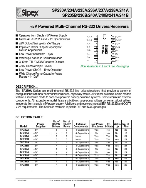
■Operates from Single +5V Power Supply ■Meets All RS-232D and V.28 Specifications ■±9V Output Swing with +5V Supply ■Improved Driver Output Capacity for Mouse Applications■Low Power Shutdown – 1µA■WakeUp Feature in Shutdown Mode ■3–State TTL/CMOS Receiver Outputs ■±30V Receiver Input Levels■Low Power CMOS – 5mA Operation ■Wide Charge Pump Capacitor Value Range – 1-10µFDESCRIPTION…The SP230A Series are multi–channel RS-232 line drivers/receivers that provide a variety of configurations to fit most communication needs, especially where ±12V is not available. Some models feature a shutdown mode to conserve power in battery-powered systems. Some require no external components. All, except one model, feature a built-in charge pump voltage converter, allowing them to operate from a single +5V power supply. All drivers and receivers meet all EIA RS-232D and CCITT V.28 requirements. The Series is available in plastic DIP and SOIC packages.SELECTION TABLET OUT T OUT T IN T IN V- C - C + C -34221T OUT T OUT T IN T IN GND V C + V+12CC 12134Now Available in Lead Free Packaging元器件交易网ABSOLUTE MAXIMUM RATINGS This is a stress rating only and functional operation of the device at these or any other conditions above those indicated in the operation sections of this specification is not implied. Exposure to absolute maximum rating conditions for extended periods of time may affect reliability.VCC ...............................................................................................................................................................+6VV+...................................................................................................................(Vcc–0.3V) to +13.2V V–.............................................................................................................................................................13.2V Input Voltages:T IN .......................................................................................................................–0.3 to (Vcc +0.3V)RIN ............................................................................................................................................................±30VOutput Voltages:TOUT.................................................................................................(V+, +0.3V) to (V–, –0.3V)ROUT..............................................................................................................–0.3V to (Vcc +0.3V)Short Circuit Duration:TOUT.........................................................................................................................................ContinuousPower Dissipation:CERDIP..............................................................................675mW(derate 9.5mW/°C above +70°C)Plastic DIP..........................................................................375mW(derate 7mW/°C above +70°C)Small Outline......................................................................375mW(derate 7mW/°C above +70°C)ELECTRICAL CHARACTERISTICS元器件交易网0V 5V 0V5V 0V0VT INT INT OUTT OUTR L = 3k Ω, C L = 2,500pFNo loadTransmitter Propagation DelayTransmitter Output WaveformsReceiver Output WaveformShutdown to V+, V– Rise TimeInOut5V 0V 0VSDV +V –Rise TimeR L = 3k Ω; C L = 2,500pF All inputs = 20kHzT INT OUTT INT OUTFall TimeR L = 3k Ω; C L = 2,500pFReceiver Propagation DelayRIN 5V 0VR OUT5V 0VR IN5V 0VR OUTPINOUTFall Time Rise TimeReceiver Output Enable/Disable TimesDisable5V 0V5V 0VEN INR OUTEnable5V 0V5V 0VEN INR OUTPINOUTFEATURES…The multi–channel RS-232 line drivers/receivers pro-vides a variety of configurations to fit most communi-cation needs, especially those applications where ±12V is not available. The SP230A, SP235A/B, SP236A/B, SP240A/B, and SP241A/B feature ashutdown mode which reduces device power dissipa-tion to less than 5µW. All feature low power CMOS operation, which is particularly beneficial in battery-powered systems. The SP235A/B use no external components and are ideally suited where printed circuit board space is limited.All products in the Series include two charge pump voltage converters which allow them to operate from a single +5V supply. These converters convert the +5V input power to the ±10V needed to generate the RS-232 output levels. An internal charge pump converter produces the necessary –12V supply. All drivers and receivers meet all EIA RS-232D and CCITT V.28 specifications.The Series are available for use over the commer-cial, industrial and military temperature ranges. They are packaged in plastic DIP and SOIC packages. For product processed and screened to MIL–M–38510 and MIL–STD–883C require-ments, please consult the factory.THEORY OF OPERATIONThe SP230A/B–241A/B series devices are made up of t hree b asic c ircuit b locks –1) t ransmitter, 2) r eceiver and 3) charge pump. Each model within the series incorporates variations of these circuits to achieve the desired configuration and performance.Driver/TransmitterThe drivers are inverting transmitters, which accept TTL or CMOS inputs and output the RS-232 signals with an inverted sense relative to the input logic levels. Typically the RS-232 output voltage swing is ±9V. Even under worst-case loading conditions of 3kΩand 2500pF, the output is guaranteed to be ±5V, which is consistent with the RS-232 standard specifications. The transmitter outputs are protected against infi-nite short-circuits to ground without degradation in reliability.The drivers of the SP230A, SP235A/B, SP236A/B, SP240A/B and SP241A/B can be tri-stated by using the SHUTDOWN function. In this “power-off” state, the output impedance will remain greater than 300 Ohms, again satisfying the RS-232 specifications. Should the input of the driver be left open, an internal 400kΩ pull–up resistor to VCCforces the input high, thus committing the output to a low state.The slew rate of the transmitter output is internally limited to a maximum of 30V/µs in order to meet theTable 1. EIA Standards Definition 元器件交易网Charge Pump Output Loading versus VCC; a) V+; b) V–ENABLE Input (EN)The SP235A/B , SP236A/B , SP240A/B, and SP241A/B all feature an enable input (EN),which allows the receiver outputs to be either tri–stated or enabled. The enable input is active outputs. This can be especially useful when the receiver is tied directly to a microprocessor data bus.Protection From Shorts to >±15VThe driver outputs are protected against shorts to ground, other driver outputs, and V + or V -.For protection against voltages exceeding ±15V,two back–to–back zener diodes connected to clamp the outputs to an acceptable voltage level are recommended. (Refer to Figure 3.)Improved Drive Capability for Mouse ApplicationsEach of the devices in this data sheet have improved drive capability for non-standard ap-plications. Although the EIA RS-232D stan-dards specify the maximum loading to be 3k Ωand 2500pF, the SP230A , SP234A , SP235A/B ,SP236A/B , SP237A , SP238A , SP240A/B, and SP241A/B can typically drive loads as low as 1k Ω and still maintain ±5V outputs. This feature is especially useful when the serial port is in-tended to be used for a “self-powered” mouse.In this case the voltage necessary to operate the circuits in the mouse can be derived from the RS-232 driver output as long as the loading is ≥1k Ω (refer to Figure 4). For applications which even exceed this requirement, drivers can be connected in parallel, increasing the drive capa-bility to 750Ω, while maintaining the ±5V V OH and V OL levels (refer to Figure 5).Figure 3. High Voltage Short Circuit ProtectionFigure 2. Charge Pump Voltage Inverter output impedance of V + and V -, which will degrade V OH and V OL . Capacitor values can be as low as 1.0µF.Shutdown (SD)The SP230A , SP235A/B , SP236A/B , SP240A/B and SP241A/B all feature a control input which will disable the part and reduce V CC current typically to less than 5µA, which is especially useful to designers of battery–pow-ered systems. In the “power–off” mode the receiver and transmitter will both be tri-stated.V + will discharge to V CC , and V - will discharge to ground.For complete shutdown to occur and the 10µA current drain to be realized, the following con-ditions must be met:• +5.00V must be applied to the SD pin;• ENABLE must either 0V, +5.0V or not connected;• the transmitter inputs must be either +5.0V or not connected;• V CC must be +5V;• Receiver inputs must be >0V and <+5VPlease note that for proper operation, the SD input pin must never be left floating.Table 2. Wake–Up Truth TableFigure 4. Mouse Application Drive Capability 10 9 8 7 6 5 4 3 2 1 0V O L /V O H (V o l t s )246810121820I OL /I OH (mA)161422V OL vs I OLV OH vs I OHFigure 5. Parallel DriversWake-Up FeatureThe SP235B , SP236B , SP240B and SP241B have a wake-up feature that keeps all receivers in an enabled state when the device is in the shutdown mode. Table 2 defines the truth table for the wake-up function. Timing for the wake-up function is shown in Figure 6.If the SP235B , SP236B , SP240B and SP241B are powered up in the shutdown state (SD driven high during V CC power up), the part must remain in a powered on state for a minimum of 3ms before the wake-up function can be used. After the 3ms wait time, there is a 2ms delay time before data is valid for both enable and disableFigure 6. Wake–Up and Shutdown Timing元器件交易网of the charge pump. If the SP2XXB is powered up with SD low, then only the 2ms delay time will apply (refer to Figure 6). Under normal operation, both the wait time and delay time should be transparent to the user.With only the receivers activated, the device typically draws less than 5µA (10µA max) sup-ply current. In the case of a modem interfaced to a computer in power-down mode, the RI (ring indicator) signal from the modem would be used to “wake up” the computer, allowing it to accept the data transmission.After the ring indicator signal has propagated through the SP2XXB receiver, it can be used to trigger the power management circuitry of the computer to power up the microprocessor and bring the SD pin to the SP2XXB low, taking it out of shutdown. The receiver propagation de-lay is typically 1µs. The enable time for V+ and V- is typically 2ms. After V+ and V- have settled to their final values, a signal can be sent back to the modem on the DTR (Data Terminal Ready) pin signifying that the computer is ready to accept and transmit data.All receivers that are active during shutdown maintain 500mV (typ.) of hysteresis.Varying Capacitor ValuesAs stated earlier, the capacitor values are some-what non-critical. Since they are an actual compo-nent of the charge pump circuitry, their value will affect its performance, which in turn affects the V OH and V OL levels. There is no upper limit for the value of any of the four capacitors; lower values will impact performance. C 1 and C 2 are respon-sible for the charge accumulation and can be reduced to 1µF; this will increase the output im-pedance of V + and V –. Reducing these capacitor values will limit the ability of the SP2XXA/B to maintain the dc voltages needed to generate the RS-232 output levels. Capacitors C 3 and C 4 can also be reduced to 1µF; doing so will increase the ripple on V + and V–.Typically each driver will require 1µF of capaci-tance as a minimum to operate within all specified parameters; if five drivers are active in the circuit,then C 3 and C 4 should be 5µF. In order to operateat these minimum values, the supply voltage must be maintained at +5.0V ±5%. Also, the ambient operating temperature must be less than 60°C.The capacitor values must be chosen to suit the particular application. The designer must bal-ance board space, cost and performance to maxi-mize the design. The capacitors can be polarized or non–polarized, axial-leaded or surface-mount.As the size and value decrease, so does the cost;however, the value should be chosen to accom-modate worst-case load conditions.IBM Modem Port InterconnectionsINTERFACE EXAMPLE – A MODEM ON THE IBM PC SERIAL PORTThe RS-232 standard defines 22 serial interface signals. These signals consist of ground lines,timing, data, control and test signals, plus a set of signals rarely used for a second data channel.Many of these signal lines are not used in typical RS-232 applications; in fact, the IBM ® PC serial port is implemented using only nine pins.For example, consider the case of a PC using this nine pin port to communicate with a peripheral device such as a modem. We see the following activity on each of the RS-232 lines as the computer and modem are activated and commu-nicate with each other as well as the remote modem at the other end of the phone line.Signal Ground (GND)The Signal Ground pin acts as a reference for all the other signals. This pin is simply maintained at a 0V level to serve as a level to which all other signals are referenced. Both the PC and the modem will have this line connected to their respective internal ground lines.元器件交易网Data Terminal Ready (DTR)This is the pin the computer uses to tell periph-eral devices that it is on–line and ready to communicate.Data Set Ready (DSR)Peripheral devices use this line to tell the com-puter that they are on–line and ready to commu-nicate. When the modem is turned on and has completed its self–test routine (assuming it does one), it will send a signal to the PC by asserting this line.Request To Send (RTS)The computer activates this line to notify the peripheral device that it is ready to send data. In this example, the computer notifies the modem that it is ready to send data to be transmitted by the modem.Clear To Send (CTS)This is the line on which the peripheral device tells the computer that it is ready to receive data from the computer. If the modem was not ready, i.e. it was performing a loop–back self–test, for example, it would not assert this line. Once the modem was ready to receive data from the PC, it would assert this line. When it receives the CTS signal from the modem, the PC knows that a data transmission path has been established between itself and the modem.Transmitted Data (TD or TX)This is the pin on which the computer sends the actual data signal to be transmitted, i.e. a posi-tive voltage (+3V to +15V) to represent a logic “0”, and a negative voltage (–3V to –15V) to represent a logic “1”. The PC would send the data on this line to be transmitted by the modem. Ring Indicator (RI)This line is used by the peripheral device to tell the computer that a remote device wants to start communicating. The modem would activate the RI line to tell the computer that the remote modem was calling, i.e. the phone is ringing. Data Carrier Detect (DCD)This line is used by the modem to tell the computer that it has completed a transmission path with the remote modem, and to expect to start receiving data at any time.Received Data (RD or RX)This is the pin on which the modem sends the computer the incoming data signal, i.e. a posi-tive voltage (+3V to +15V) to represent a logic “0”, and a negative voltage (-3V to -15V) to represent a logic “1”.INTERFACE EXAMPLE – A PRINTER ON THE IBM PC SERIAL PORTThe RS-232 standard defines 22 serial interface signals. These signals consist of ground lines, timing, data, control and test signals, plus a set of signals rarely used for a second data channel. Many of these signal lines are not used in typical RS-232 applications; in fact, the IBM® PC serial port is implemented using only nine pins.For example, consider the case of a PC using this nine pin port to communicate with a peripheral device such as a printer. We see the following activity on each of the RS-232 lines as the com-puter and printer are activated and communicate. Signal Ground (GND)The Signal Ground pin acts as a reference for all the other signals. This pin is simply maintained at a 0V level to serve as a level to which all other signals are referenced. Both the PC and the printer will have this line connected to their respective internal ground lines.Data Terminal Ready (DTR)This is the pin the computer uses to tell peripheral devices that it is on–line and ready to communi-IBM Printer Port Interconnections元器件交易网cate. Once the computer is powered–up and ready, it will send out a signal on the DTR to inform the printer that it is powered–up and ready to go. The printer really doesn’t care, since it will simply print data as it is received. Accordingly, this pin is not needed at the printer.Data Set Ready (DSR)Peripheral devices use this line to tell the computer that they are on–line and ready to communicate. When the printer is turned on and has completed its self–test routine (assuming it does one), it will send a signal to the PC by asserting this line. Request To Send (RTS)The computer activates this line to notify the peripheral device that it is ready to send data. In this example, the computer notifies the printer that it is ready to send data to be printed by the printer. Clear To Send (CTS)This is the line on which the peripheral device tells the computer that it is ready to receive data from the computer. If the printer was not ready, i.e. it was out of paper, for example, it would not assert this line. Once the printer was ready to receive data from the PC, it would assert this line. When it receives the CTS signal from the printer, the PC knows that a data transmission path has been established between itself and the printer. Transmitted Data (TD or TX)This is the pin on which the computer sends the actual data signal representing the actual informa-tion to be printed, i.e. a positive voltage (+3V to +15V) to represent a logic “0”, and a negative voltage (-3V to -15V) to represent a logic “1”. Ring Indicator (RI)This line is used by the peripheral device to tell the computer that a remote device wants to start com-municating. A modem would activate the RI line to tell the computer that a remote modem was calling, i.e. the phone is ringing. In the case of a printer, this line is unused.Data Carrier Detect (DCD)This line is used by a peripheral device to tell the computer to expect to start receiving data at any time. Since the printer would not be sending data to the PC in this case this line is not needed.Received Data (RD or RX)This is the pin on which the computer receives the incoming data signal, i.e. a positive voltage (+3V to +15V) to represent a logic “0”, and a negative voltage (-3V to -15V) to represent a logic “1”. Again, in this instance, since the printer will not be sending the PC any data, this line is not needed.元器件交易网ORDERING INFORMATIONModel .......................................................................................Temperature Range....................................................................PackageSP230ACP .....................................................................................0°C to +70°C ...............................................................................20 pin PDIP SP230ACT .....................................................................................0°C to +70°C ............................................................................20 pin WSOIC SP230ACT/TR ...............................................................................0°C to +70°C ............................................................................20 pin WSOIC SP230ACX .....................................................................................0°C to +70°C ............................................................................................Dice SP230AEP ...................................................................................–40°C to +85°C .............................................................................20 pin PDIP SP230AET ...................................................................................–40°C to +85°C ..........................................................................20 pin WSOIC SP230AET/TR .............................................................................–40°C to +85°C ..........................................................................20 pin WSOIC SP234ACP .....................................................................................0°C to +70°C ...............................................................................16 pin PDIP SP234ACT .....................................................................................0°C to +70°C ............................................................................16 pin WSOIC SP234ACT/TR ...............................................................................0°C to +70°C ............................................................................16 pin WSOIC SP234ACX .....................................................................................0°C to +70°C ............................................................................................Dice SP234AEP ...................................................................................–40°C to +85°C .............................................................................16 pin PDIP SP234AET ...................................................................................–40°C to +85°C ..........................................................................16 pin WSOIC SP234AET/TR .............................................................................–40°C to +85°C ..........................................................................16 pin WSOIC SP235ACP .....................................................................................0°C to +70°C ...............................................................................24 pin PDIP SP235AEP ...................................................................................–40°C to +85°C .............................................................................24 pin PDIP SP235BCP .....................................................................................0°C to +70°C ...............................................................................24 pin PDIP SP235BEP ...................................................................................–40°C to +85°C .............................................................................24 pin PDIP SP236ACS .....................................................................................0°C to +70°C ...............................................................................24 pin PDIP SP236ACT .....................................................................................0°C to +70°C ............................................................................24 pin WSOIC SP236ACT/TR ...............................................................................0°C to +70°C ............................................................................24 pin WSOIC SP236ACX .....................................................................................0°C to +70°C ............................................................................................Dice SP236AES ...................................................................................–40°C to +85°C .............................................................................24 pin PDIP SP236AET ...................................................................................–40°C to +85°C ..........................................................................24 pin WSOIC SP236AET/TR .............................................................................–40°C to +85°C ..........................................................................24 pin WSOIC SP236BCS .....................................................................................0°C to +70°C .............................................................................. 24 pin PDIP SP236BCT .....................................................................................0°C to +70°C ............................................................................24 pin WSOIC SP236BCT /TR ..............................................................................0°C to +70°C ............................................................................24 pin WSOIC SP236BCX .....................................................................................0°C to +70°C ............................................................................................Dice SP236BES ...................................................................................–40°C to +85°C .............................................................................24 pin PDIP SP236BET ...................................................................................–40°C to +85°C ..........................................................................24 pin WSOIC SP236BET /TR ............................................................................–40°C to +85°C ..........................................................................24 pin WSOIC SP237ACS .....................................................................................0°C to +70°C ...............................................................................24 pin PDIP SP237ACT .....................................................................................0°C to +70°C ............................................................................24 pin WSOIC SP237ACT/TR ...............................................................................0°C to +70°C ............................................................................24 pin WSOIC SP237ACX .....................................................................................0°C to +70°C ............................................................................................Dice SP237AES ...................................................................................–40°C to +85°C .............................................................................24 pin PDIP SP237AET ...................................................................................–40°C to +85°C ..........................................................................24 pin WSOIC SP237AET/TR .............................................................................–40°C to +85°C ..........................................................................24 pin WSOIC/TR = Tape and ReelPack quantity is 1,500 for WSOIC.Available in lead free packaging. To order add "-L" suffix to part number.Example: SP230AEP = standard; SP230AEP-L = lead free Please consult factory for SP235B, SP236B, SP240B, SP241B, and dice.CorporationANALOG EXCELLENCESipex Corporation Headquarters and Sales Office233 South Hillview Drive Milpitas, CA 95035TEL: (408) 934-7500FAX: (408) 935-7600元器件交易网。
EPM240T100I中文资料(Altera)中文数据手册「EasyDatasheet - 矽搜」

LEs
240
570
1,270
2,210
240
570
典型等效宏单元
192
440
980
1,700
192
440
等效宏单元范围
128 to 240 240 to 570 570 to 1,270 1,270 to 2,210 128 to 240 240 to 570
UFM大小(位)
8,192
8,192
8,192
BGA
BGA
BGA
BGA
0.5
0.5
1
1
49
121
289
361
7×7
11 × 11 17 × 17 19 × 19
■ UFM block up to 8 Kbits for non-volatile storage ■ MultiVolt 核心 enabling external supply voltages to the device of either 3.3 V/2.5 V
or 1.8 V
■ MultiVolt I/O interface supporting 3.3-V, 2.5-V, 1.8-V, and 1.5-V logic levels
表1-4. MAX II TQFP,BGAFineLine和Micro BGAFineLine包装规格
包裹
间距(mm) 面产品(mm2) 长×宽 (毫米×毫米)
68-Pin 100-Pin
Micro Micro 100-Pin
FineLine FineLine FineLine 100-Pin
BGA
EPM570
—
76
MC-4系列说明书 (1)

• 使检测仪进入校准操作,按住 C,检测仪先完成OFF倒计时,继续按住C,显示屏暂时关闭,
然后出现CAL倒计时。CAL倒计时完成后放开C。
• 开启背景照明灯,按 C。 • 确认已锁定的报警,按 C。
5
GasAlertMicroClip 气体检测仪操作指南
校准
步骤
1. 在清洁空气环境下,按住C直至屏幕出 现OFF倒计时,检测仪暂时关闭后时继 续按住C。
H2S: 0至100 ppm (1 ppm 增量) CO: 0至500 ppm (1 ppm 增量) O2: 0至30.0% vol. (0.1% vol.增量) 可燃气体(LEL): 0至100% (1%增量) 传感器类型: H2S, CO, O2:单一插拔式电化学电池 可燃气体:插拔式催化珠 氧气检测原理:毛细管控制浓度传感器
2. 检测仪重新启动,屏幕显示CAL倒计 时,按住C直至倒计时结束并进入校准 状态。
3.
闪烁,此时检测仪开始将
所有传感器归零,并对氧气传感器进
行校准。如自动归零失败,则不能进
行跨度调整。自动归零完成后,屏幕
显示APPLY GAS(施加标气)。
显示
步骤
4. 接通标气气瓶且以250-500ml/min流
正常关机:
• 四次“ 嘟” 音和四次闪光 • 震动报警器暂时性启动
GasAlertMicroClip 报警
屏幕显示
注意 报警方式可设置成锁定模式或非锁定模式。进入GasAlertMicroClip菜单的警报锁定选项可确认设定。地方法规有可能要求检测仪须使 用锁定报警模式。 如果检测仪设置为静音模式,在报警条件出现时只有震动报警启动(听觉报警和视觉报警均被关闭);如检测仪设置为IR静音模式, 则视觉报警和震动报警启动(听觉报警关闭)。 背景灯在任何报警条件下均启动。
- 1、下载文档前请自行甄别文档内容的完整性,平台不提供额外的编辑、内容补充、找答案等附加服务。
- 2、"仅部分预览"的文档,不可在线预览部分如存在完整性等问题,可反馈申请退款(可完整预览的文档不适用该条件!)。
- 3、如文档侵犯您的权益,请联系客服反馈,我们会尽快为您处理(人工客服工作时间:9:00-18:30)。
Key Features• Inverted Video Signals (magnitude increases in a negative direction)• Light source, lens, and sensor are integrated into a single module • 8 dpm resolution• 216 mm scanning length• 0.347ms/line scanning speed, operated @ 5.0MHz • Wide dynamic range Analog output • 660nm light source• Compact size: ≈ 14 mm 19.5 mm x 232 mm • Low power • Light weightGeneral DescriptionThe PI240MC-A4 is a contact imaging sensor, CIS, module, which is composed of 1728PI3020 sensor chips. The PI3020 is a 200 DPI solid-state line imaging array, also a product of Peripheral Imaging Corporation. This imaging device is fabricated using MOS imaging sensor technology for high-speed performance and high sensitivity. The PI240MC-A4 is suitable for scanning A4 size (216 mm) documents with 8 dots per millimeter resolution. Applications include variety of document scanners, variety of mark readers, and other automation equipment.Functional DescriptionThe PI240MC-A4 imaging array consists of 27 chips that are cascaded to provide 1728 photo-detectors with their associated multiplex switches, and a digital shift register that controls its sequential readout. Mounted in the module is one-to-one gradedindexed micro lens array that focuses the scanned documents to image onto itssensing plane. The on-board amplifierprocesses the video signal to produce a sequential stream of video at the video output pin of the PI240MC-A4 module.Figure 1. PI240MC-A4 Cross Section200DPI CIS ModuleEngineering Data SheetPeripheral ImagingCorporationPI240MC-A4GLASS WINDOWDOCUMENT SURFACELIGHT PATH SENSORSPCB L E D B A R R O D L E N SM O D U L E H O U S EINSIDE PICTORIAL OF MODULEIllumination is by means of an integrated LED light source. All components are housed in a small plastic housing which has a cover glass which acts as the focal point for the object being scanned andprotects the imagingarray, micro lensassembly, and LED light source from dust. I/O to the module is the 10-pin connector located on oneend of the module. See Figure 4. The Mechanical Structure.The cross section of thePI240MC-A4 is shown inFigure 1 and the block diagram in Figure 2.Recommended Operating Conditions (25 °C)ItemSymbol Min Typical Max Units Vdd 4.5 5.0 5.5V Idd 243035ma Vn -4.5-5-15V Ivn 568ma VLED 4.5 5.0 5.5V Power SupplyILED 305430560ma Video Output LevelVid 0.81.01.2V Input voltage at digital high Vih Vdd -1.0Vdd -0.5Vdd V Input voltage at digital low Vil 00.8V Clock frequencyF 3.05.0MHz Clock pulse high duty cycle 25%Clock pulse high duration 50ns Integration timeTint (1)0.3460.610.0ms Operating temperatureTop25500CNote (1). Tint is determined by time interval between two start pulses, SP. The longest integration time is determined by the degree of leakage current degradation that can betolerated by the system. A 10ms maximum is a typical rule-of-thumb hence the experienced CIS user can use his discretion in determining the integration time.Figure 2. PI240MC-A4 Module Block DiagramElectro-Optical Characteristics (25° C)Parameter Symbol Parameter Units NoteNumber of photo detectors1728elementsPixel-to-pixel spacing125µmLine scanning rate(1)Tint347µsec@ 5.0 MHzclockfrequency Clock frequency(2)freq 5.0MHzBright output voltage(3)Vp 1.0VoltsBright outputUp<+/-30%nonuniformity(4)Adjacent pixelUadj<25%nonuniformity(5)Dark nonuniformity(6)Ud<100mVDark output voltage(6)Vd<150mVMTF>30%Modulation transferfunction(7)Definition:(1) Tint: line scanning rate or integration time. Tint is determined by the interval of two start pulses (SP).(2) freq is the main clock frequency.(3) Vpavg = ∑ Vp(n)/1728(4) Up = [(Vpmax - Vp) / Vp] x 100% or [(Vp - Vpmin) / Vp] x 100%(5) Upadj = MAX[ | (Vp(n) - Vp(n+l) | / Vp(n)] x 100%Upadj is the nonuniformity percentage of adjacent pixels(6) Ud = Vdmax - VdminVd is the voltage amplitude between the output video's reset level and its dark level. Vdmin is the minimum output with LED light off.Vdmax: maximum output voltage with the LED light off.(7) MTF = [(Vmax - Vmin) / (Vmax + Vmin)] x 100 [%]Vmax: maximum output voltage at 4.0 lp/mmVmin: minimum output voltage at 4.0 lp/mm(8) lp / mm: line pair per mmSwitching Characteristics (250C)Figure 3Symbol Definitions for the Above Timing DiagramItemSymbol Min. TypicalMax. Units Clock cycle time to 0.2 4.0s Clock pulse width tw 50ns Clock duty cycle2575%Prohibit crossing time of Start Pulse tprh 15ns Data setup time tds 20ns Data hold time tdh 20ns Signal delay time tdl 50ns Signal settling timetsh90nsMODULE TIMING DIAGRAMCPSP tds VoutAbsolute Maximum Rating:Parameter Symbols Maximum Rating UnitsPower supply voltageVdd10VIdd30mAVn-15VIn15mAVLED6VILED650ma Input clock pulse (high level)Vih Vdd – 0.5V VInput clock pulse (low level)Vil-0.5VNote (1): These parameters are absolute maximums and should not be used to operate the module.Operating EnvironmentOperating temperature Top0 to 500C Operating humidity Hop10 to 85%Storage temperature Tstg-25 to+750CStorage humidity Hstg10 to 90% Mechanical ConsiderationsI/O Connector Pin configurationConnector is a 1.25mm 10 pin JAE IL-Z-10P-S125L3-E. Its location, along with its pin1 location, are shown in Figure 4 The Mechanical Structure.Pin Number Symbol Names and Functions1Vout Analog video output2Gnd Ground; 0V3Vdd (+5V)Positive power supply4Vn (-5V to –12V)Negative power supply5Gnd Ground; 0V6SP Shift register start pulse7Gnd Ground; 0V8CP Sampling clock pulse9GLED Ground for the light source; 0V10VLED Supply for the light sourceModule Housing DimensionsThe PI240MC-A4 module outline and its mechanical dimensions are shown. A detailed housing drawing is available upon request.ALL DIMENSIONS IN MM UNLESS OTHERWISE SPECIFIEDMECHANICAL STRUCTUREFIGURE 4©2001 Peripheral Imaging Corporation.Printed in USA. All rights reserved. Specificationsare subject to change without notice. Contents may not be reproduced in whole or in part without the express prior written permission of Peripheral Imaging Corporation. Information furnished herein is believed to be accurate and reliable. However, no responsibility is assumed by Peripheral Imaging Corporation for its use nor for any infringement of patents or other rights granted by implication or otherwise under any patent or patent rights of Peripheral Imaging Corporation.。