LM78LM中文资料
78L05中文资料_数据手册_参数

LM78LXX系列三端正稳压器一般描述 LM78LXX系列三端正向稳压器是可用几个固定的输出电压使他们在广泛的应用中 有用.当用作齐纳二极管/电阻组合替代,LM78LXX usu-盟友导致有效的输出阻抗改善两个数量级以及更低的静态电流.这 些监管机构可以提供当地的卡规,消除与单点规则相关的分配问题 - 灰.可用电压允许LM78LXX用于逻辑系统,仪器仪 表,HiFi等固态电子设备. LM78LXX采用塑料TO-92(Z)封装,塑料SO-8(M)封装和芯片尺寸封装 (8-Bump micro SMD)采用美国国家半导体的微型SMD封装技术.如果有足够的散热片,肝脏100毫安输出电流.电流限制包括在内将峰 值输出电流限制在安全值.安全区域pro-提供对输出晶体管的检测以限制内部功耗.如果内部功耗变得太大高散热提供, 热关断CIR - cuit接管防止IC过热.特征 ? LM78L05采用微型SMD封装 ? 输出电压容差 在整个温度 范围内的 ± 5%范围 ?输 出电流100毫安 ?内部热过载保护 ?输出晶体管安全区域保护 ?内部短路电流限制 ?提供塑料TO-92和塑料SO-8低轮廓包 ?没 有外部元件 ?输出电压为5.0V,6.2V,8.2V,9.0V,12V,15V连接图 SO-8塑料(M) (窄体) DS007744-2顶视图 8凹凸 微型SMD DS007744-24顶视图 (凹凸面朝下) (TO-92)塑料包装(Z) DS007744-3底视图微型SMD标记方向 DS007744-33顶视图 可用性和规格.功耗(注5)内部限制输入电压 35V储存温度 -65?C至+150?C工作结温 SO-8 0?C至125?C微型SMD -40?C至 85?C焊接信息红外或对流(20秒) 235C波峰焊接(10秒) 260?C(提前期) ESD敏感度(注2)千伏 LM78LXX电气特性 标准字体的限制是T J =25?C,粗体字ap- SO-8封装的工作温度范围为0?C至125?C,微型SMD封装的工作温度范围为-40?C 至85?C.限制由产品保证,使用标准的统计质量控制(SQC)方法进行测试或相关技术.除非另有说明:I ? = 40毫安,C I =0.33μF,C0 =0.1μF. LM78L05除非另有规定,V IN = 10V符号参数条件敏典型马克斯单位 V ?输出电压 4.8五 5.2 V 7V ≤V IN≤20V 1毫安 ≤我 O≤40 mA (注3) 4.75 5.25 1毫安 ≤我 O≤70 mA (注3) 4.75 5.25 ΔV ?线路调整 7V ≤V IN≤20V 18 75毫伏 8V ≤V IN≤20V 10 54 ΔV ?负载调节 1毫安 ≤我 O≤100 mA 20 60 1毫安 ≤我 O≤40 mA五三十一世 Q 静态电流 3五 ΔI Q静态电流变化 8V ≤V IN≤20V 1.0 1毫安 ≤我 O≤40 mA 0.1 V ?输出噪声电压 f = 10Hz至100kHz (注 4) 40 μV波纹拒绝 f = 120Hz 8V ≤V IN≤16V 47 62 D b一世 PK峰值输出电流 140嘛平均输出电压温度系数一世 O = 5mA -0.65毫伏/℃ V IN (小)输入电压的小值保持线路规定所需 6.7 7 V θ JA热阻 (8凹凸微型SMD) 230.9 C / W LM78L62AC除非另有规定,V IN = 12V符号参数条件敏典型马克斯单位 V ?输出电压 5.95 .2 6.45 V 8.5V ≤V IN≤20V 1毫 安 ≤我 O≤40 mA (注3) 5.9 6.5 1毫安 ≤我 O≤70 mA (注3) 5.9 6
LM78L12A中文资料

Unit V mV
mV
Load Regulation
∆VO TJ = 25 °C
1mA ≤ IO ≤ 100mA - 15 80 mV
1mA ≤ IO ≤ 40mA
- 8.0 40 mV
10.5V ≤ VI ≤ 23V 1mA ≤ IO ≤ 40mA 7.6 - 8.4
V
Output Voltage
TJ = 25 °C
Min. Typ. Max. Unit
4.8 5.0 5.2 V
-
8 150 mV
-
6 100 mV
- 11 60 mV
- 5.0 30 mV
-
- 5.25 V
4.75 - 5.25 V
- 2.0 5.5 mA
-
- 1.5 mA
-
- 0.1 mA
- 40 -
µV
- -0.65 - mV/ °C
VO
14.5V ≤ VI ≤ VMAX (Note 2)
1mA ≤ IO ≤ 70mA
11.4
-
12.6
V
Quiescent Current
IQ
TJ = 25 °C
- 2.1 6.0 mA
Quiescent Current with line
∆IQ 16V ≤ VI ≤ 27V
Change
with load ∆IQ 1mA ≤ IO ≤ 40mA
THERMAL SHUTDOWN CIRCUIT
SHORT CIRCUIT PROTECTION
RSC
OVu0 tput
1
©2000 Fairchild Semiconductor International
LM78L09F中文资料

3-TERMINAL 0.1A POSITIVE VOLTAGE REGULATORSThis series of fixed-voltage monolithic integrated-circuitvoltage regulators is designed for a wide range ofapplications.These applications include on-card regulation forelimination of noise and distribution problems associatedwith single-point regulation.In addition, they can be used with power-pass elementsto make high current voltage regulators.Each of these regulators can deliver up to 100㎃ of outputcurrent.The internal limiting and thermal shutdown features ofthese regulators make them essentially immune to overload.When used as a replacement for a zener diode-resistor com-bination, an effective improvement in output impedancecan be obtained together with lower-bias current.ORDERING INFORMATIONDevice Marking PackageLM78LXX LM78LXXTO-92 FEATURES LM78L05 /A /C LM78L05 /A /C◇ Output Current Up to 100㎃LM78L05NF805SOT-89◇ No External Components LM78L05AF/CF◇ Internal Thermal Overload Protection LM78L06F~24F806~824◇ Internal Short-Circuit Limiting XX = Output Voltage or Grade◇ Output Voltage of 5V, 6V, 8V, 9V, 10V, 12V, 15V, 18Vand 24VABSOLUTE MAXIMUM RATINGSCharacteristic Symbol Value UnitInput voltage LM78L05 /A/C∼ LM78L10V I30V LM78L12 ∼ LM78L1835LM78L2440Operating junction temperature Topr0 ∼ +150℃Storage temperature Tstg-65 ∼ +150Soldering temperature and time Tsol260/10secMar. 2006 - Rev 06 HTCRECOMMENDED OPERATING CONDITIONSMin.Max.UnitInput Voltage V I7LM78L05 / A / C20V LM78L06820LM78L0810.523LM78L0911.524LM78L1012.525LM78L1214.527LM78L1517.530LM78L1820.533LM78L2426.539Output current,Io100㎃perating virtual junction temperature, 0125℃TYPICAL APPLICATIONNotes1. To specify an output voltage, substitute voltage for "XX"2. Bypass capacitors are recommended for optimum stability and transient response and should be located as close as possible to the regulators.LM78L05 ELECTRICAL CHARACTERISTICS(At specified virtual junction temperature, V I=10V, I O=40㎃ (unless otherwise noted)Characteistic Symbol Test condition *Min.Typ.Max.UnitOutput voltage **V OUT25℃ 4.85 5.21㎃≤I O≤40㎃0℃ ∼ 125℃4.7555.25V 7V≤V I≤20V1㎃≤I O≤70㎃ 4.755 5.25Line regulation Reg line 7V≤V I≤20V25℃32150㎷8V≤V I≤20V26100Load regulation Reg load 1㎃≤I O≤100㎃25℃1560㎷1㎃≤I O≤40㎃830Bias current I B25℃ 3.86㎃125℃ 5.5Bias current change△I B9V≤V I≤20V0℃ ∼ 125℃ 1.5㎃1㎃≤I O≤40㎃0.1 Output noise voltage V N10Hz≤f≤100kHz25℃42㎶Ripple rejection RR 8V≤V I≤18Vf=120Hz25℃4149㏈Dropout voltage V D25℃ 1.7VNotes*. Pulse testing techniques are used to maintain the junction temperature as close to theambient temperature as possible.Thermal effects must be taken into account separately.All characteristics are measured with a 0.33㎌ capacitor across the input and a 0.1㎌capacitor across the output.**. This specification applies only for DC power dissipation permitted by absolute maximumratings.Mar. 2006 - Rev 06 HTCLM78L05A ELECTRICAL CHARACTERISTICS(At specified virtual junction temperature, V I=10V, I O=40㎃ (unless otherwise noted)Characteistic Symbol Test condition *Min.Typ.Max.UnitOutput voltage **V OUT25℃ 4.95 5.11㎃≤I O≤40㎃0℃ ∼ 125℃4.955.1V 7V≤V I≤20V1㎃≤I O≤70㎃ 4.95 5.1Line regulation Reg line 7V≤V I≤20V25℃550㎷8V≤V I≤20V325Load regulation Reg load1㎃≤I O≤100㎃25℃1560㎷1㎃≤I O≤40㎃830Bias current I B25℃ 3.86㎃125℃ 5.5Bias current change△I B9V≤V I≤20V0℃ ∼ 125℃1.5㎃1㎃≤I O≤40㎃0.1Output noise voltage V N10Hz≤f≤100kHz25℃42㎶Ripple rejection RR 8V≤V I≤18Vf=120Hz25℃4149㏈Dropout voltage V D25℃ 1.7VNotes*. Pulse testing techniques are used to maintain the junction temperature as close to theambient temperature as possible.Thermal effects must be taken into account separately.All characteristics are measured with a 0.33㎌ capacitor across the input and a 0.1㎌capacitor across the output.**. This specification applies only for DC power dissipation permitted by absolute maximumratings.Mar. 2006 - Rev 06 HTCLM78L05C ELECTRICAL CHARACTERISTICS(At specified virtual junction temperature, V I=10V, I O=40㎃ (unless otherwise noted)Characteistic Symbol Test condition *Min.Typ.Max.UnitOutput voltage **V OUT25℃ 4.955 5.051㎃≤I O≤40㎃0℃ ∼ 125℃4.9555.05V 7V≤V I≤20V1㎃≤I O≤70㎃ 4.955 5.05Line regulation Reg line 7V≤V I≤20V25℃550㎷8V≤V I≤20V325Load regulation Reg load1㎃≤I O≤100㎃25℃1550㎷1㎃≤I O≤40㎃825 Bias current I B25℃ 3.86㎃125℃ 5.5Bias current change△I B9V≤V I≤20V0℃ ∼ 125℃ 1.5㎃1㎃≤I O≤40㎃0.1 Output noise voltage V N10Hz≤f≤100kHz25℃42㎶Ripple rejection RR 8V≤V I≤18Vf=120Hz25℃4149㏈Dropout voltage V D25℃ 1.7VNotes*. Pulse testing techniques are used to maintain the junction temperature as close to theambient temperature as possible.Thermal effects must be taken into account separately.All characteristics are measured with a 0.33㎌ capacitor across the input and a 0.1㎌capacitor across the output.**. This specification applies only for DC power dissipation permitted by absolute maximumratings.Mar. 2006 - Rev 06 HTCLM78L06 ELECTRICAL CHARACTERISTICS(At specified virtual junction temperature, V I=10V, I O=40㎃ (unless otherwise noted)Characteistic Symbol Test condition *Min.Typ.Max.UnitOutput voltage **V OUT25℃ 5.756 6.251㎃≤I O≤40㎃0℃ ∼ 125℃5.766.3V 8V≤V I≤20V1㎃≤I O≤70㎃ 5.76 6.3Line regulation Reg line 8V≤V I≤20V25℃35175㎷9V≤V I≤20V29125Load regulation Reg load 1㎃≤I O≤100㎃25℃1680㎷1㎃≤I O≤40㎃940Bias current I B25℃ 3.96㎃125℃ 5.5Bias current change△I B9V≤V I≤20V0℃ ∼ 125℃1.5㎃1㎃≤I O≤40㎃0.1Output noise voltage V N10Hz≤f≤100kHz25℃46㎶Ripple rejection RR 9V≤V I≤19V25℃4048㏈f=120HzDropout voltage V D25℃ 1.7VNotes*. Pulse testing techniques are used to maintain the junction temperature as close to theambient temperature as possible.Thermal effects must be taken into account separately.All characteristics are measured with a 0.33㎌ capacitor across the input and a 0.1㎌capacitor across the output.**. This specification applies only for DC power dissipation permitted by absolute maximumratings.Mar. 2006 - Rev 06 HTCLM78L08 ELECTRICAL CHARACTERISTICS(At specified virtual junction temperature, V I=14V, I O=40㎃ (unless otherwise noted)Characteistic Symbol Test condition *Min.Typ.Max.Unit25℃7.788.3Output voltage **V OUT1㎃≤I O≤40㎃0℃ ∼ 125℃7.688.4V10.5V≤V I≤23V1㎃≤I O≤70㎃7.688.4Line regulation Reg line10.5V≤V I≤23V25℃42175㎷11V≤V I≤23V36125Load regulation Reg load1㎃≤I O≤100㎃25℃1880㎷1㎃≤I O≤40㎃1040Bias current I B25℃46㎃125℃ 5.5Bias current change△I B11V≤V I≤23V0℃ ∼ 125℃ 1.5㎃1㎃≤I O≤40㎃0.1Output noise voltage V N10Hz≤f≤100kHz25℃54㎶Ripple rejection RR13V≤V I≤23V25℃3746㏈f=120HzDropout voltage V D25℃ 1.7VNotes*. Pulse testing techniques are used to maintain the junction temperature as close to theambient temperature as possible.Thermal effects must be taken into account separately.All characteristics are measured with a 0.33㎌ capacitor across the input and a 0.1㎌capacitor across the output.**. This specification applies only for DC power dissipation permitted by absolute maximumratings.Mar. 2006 - Rev 06 HTCLM78L09 ELECTRICAL CHARACTERISTICS(At specified virtual junction temperature, V I=16V, I O=40㎃ (unless otherwise noted)Characteistic Symbol Test condition *Min.Typ.Max.Unit25℃8.699.4Output voltage **V OUT1㎃≤I O≤40㎃0℃ ∼ 125℃8.5599.45V12V≤V I≤24V1㎃≤I O≤70㎃8.5599.45Line regulation Reg line12V≤V I≤24V25℃45175㎷13V≤V I≤24V40125Load regulation Reg load1㎃≤I O≤100㎃25℃1990㎷1㎃≤I O≤40㎃1140Bias current I B25℃ 4.16㎃125℃ 5.5Bias current change△I B13V≤V I≤24V0℃ ∼ 125℃ 1.5㎃1㎃≤I O≤40㎃0.1Output noise voltage V N10Hz≤f≤100kHz25℃58㎶Ripple rejection RR13V≤V I≤23V25℃3845㏈f=120HzDropout voltage V D25℃ 1.7VNotes*. Pulse testing techniques are used to maintain the junction temperature as close to theambient temperature as possible.Thermal effects must be taken into account separately.All characteristics are measured with a 0.33㎌ capacitor across the input and a 0.1㎌capacitor across the output.**. This specification applies only for DC power dissipation permitted by absolute maximumratings.Mar. 2006 - Rev 06 HTCLM78L10 ELECTRICAL CHARACTERISTICS(At specified virtual junction temperature, V I=17V, I O=40㎃ (unless otherwise noted)Characteistic Symbol Test condition *Min.Typ.Max.UnitOutput voltage **V OUT25℃9.61010.41㎃≤I O≤40㎃0℃ ∼ 125℃9.51010.5V 13V≤V I≤25V1㎃≤I O≤70㎃9.51010.5Line regulation Reg line 13V≤V I≤25V25℃51175㎷14V≤V I≤25V42125Load regulation Reg load 1㎃≤I O≤100㎃25℃2090㎷1㎃≤I O≤40㎃1140Bias current I B25℃ 4.26㎃125℃ 5.5Bias current change△I B 14V≤V I≤25V0℃ ∼ 125℃1.5㎃1㎃≤I O≤40㎃0.1Output noise voltage V N10Hz≤f≤100kHz25℃62㎶Ripple rejection RR 15V≤V I≤25Vf=120Hz25℃3744㏈Dropout voltage V D25℃ 1.7VNotes*. Pulse testing techniques are used to maintain the junction temperature as close to theambient temperature as possible.Thermal effects must be taken into account separately.All characteristics are measured with a 0.33㎌ capacitor across the input and a 0.1㎌capacitor across the output.**. This specification applies only for DC power dissipation permitted by absolute maximumratings.Mar. 2006 - Rev 06 HTCLM78L12 ELECTRICAL CHARACTERISTICS(At specified virtual junction temperature, V I=19V, I O=40㎃ (unless otherwise noted)Characteistic Symbol Test condition *Min.Typ.Max.UnitOutput voltage **V OUT25℃11.51212.51㎃≤I O≤40㎃0℃ ∼ 125℃11.41212.6V 14V≤V I≤27V1㎃≤I O≤70㎃11.41212.6Line regulation Reg line 14.5V≤V I≤27V25℃55250㎷16V≤V I≤27V49200Load regulation Reg load 1㎃≤I O≤100㎃25℃22100㎷1㎃≤I O≤40㎃1350Bias current I B25℃ 4.3 6.5㎃125℃6Bias current change△I B 16V≤V I≤27V0℃ ∼ 125℃1.5㎃1㎃≤I O≤40㎃0.1Output noise voltage V N10Hz≤f≤100kHz25℃70㎶Ripple rejection RR 15V≤V I≤25Vf=120Hz25℃3742㏈Dropout voltage V D25℃ 1.7VNotes*. Pulse testing techniques are used to maintain the junction temperature as close to theambient temperature as possible.Thermal effects must be taken into account separately.All characteristics are measured with a 0.33㎌ capacitor across the input and a 0.1㎌capacitor across the output.**. This specification applies only for DC power dissipation permitted by absolute maximumratings.Mar. 2006 - Rev 06 HTCLM78L15 ELECTRICAL CHARACTERISTICS(At specified virtual junction temperature, V I=23V, I O=40㎃ (unless otherwise noted)Characteistic Symbol Test condition *Min.Typ.Max.UnitOutput voltage **V OUT25℃14.41515.61㎃≤I O≤40㎃0℃ ∼ 125℃14.251515.75V 17.5V≤V I≤30V1㎃≤I O≤70㎃14.251515.75Line regulation Reg line 17.5V≤V I≤30V25℃65300㎷19V≤V I≤30V58250Load regulation Reg load 1㎃≤I O≤100㎃25℃25150㎷1㎃≤I O≤40㎃1575Bias current I B25℃ 4.2 6.5㎃125℃6Bias current change△I B 19V≤V I≤30V0℃ ∼ 125℃1.5㎃1㎃≤I O≤40㎃0.1Output noise voltage V N10Hz≤f≤100kHz25℃82㎶Ripple rejection RR 18.5V≤V I≤28.5Vf=120Hz25℃3744㏈Dropout voltage V D25℃ 1.7VNotes*. Pulse testing techniques are used to maintain the junction temperature as close to theambient temperature as possible.Thermal effects must be taken into account separately.All characteristics are measured with a 0.33㎌ capacitor across the input and a 0.1㎌capacitor across the output.**. This specification applies only for DC power dissipation permitted by absolute maximumratings.Mar. 2006 - Rev 06 HTC36LM78L18 ELECTRICAL CHARACTERISTICS(At specified virtual junction temperature, V I=26V, I O=40㎃ (unless otherwise noted)Characteistic Symbol Test condition *Min.Typ.Max.UnitOutput voltage **V OUT25℃17.31818.71㎃≤I O≤40㎃0℃ ∼ 125℃17.11818.9V 20.5V≤V I≤33V1㎃≤I O≤70㎃17.11818.9Line regulation Reg line 20.5V≤V I≤33V25℃70360㎷22V≤V I≤33V64300Load regulation Reg load 1㎃≤I O≤100㎃25℃27180㎷1㎃≤I O≤40㎃1990Bias current I B25℃ 4.7 6.5㎃125℃6Bias current change△I B 22V≤V I≤33V0℃ ∼ 125℃1.5㎃1㎃≤I O≤40㎃0.1Output noise voltage V N10Hz≤f≤100kHz25℃82㎶Ripple rejection RR 21.5V≤V I≤31.5Vf=120Hz25℃3236㏈Dropout voltage V D25℃ 1.7VNotes*. Pulse testing techniques are used to maintain the junction temperature as close to theambient temperature as possible.Thermal effects must be taken into account separately.All characteristics are measured with a 0.33㎌ capacitor across the input and a 0.1㎌capacitor across the output.**. This specification applies only for DC power dissipation permitted by absolute maximumratings.Mar. 2006 - Rev 06 HTC37LM78L24 ELECTRICAL CHARACTERISTICS(At specified virtual junction temperature, V I=32V, I O=40㎃ (unless otherwise noted)Characteistic Symbol Test condition *Min.Typ.Max.UnitOutput voltage **V OUT25℃2324251㎃≤I O≤40㎃0℃ ∼ 125℃22.82425.2V 26.5V≤V I≤39V1㎃≤I O≤70㎃22.82425.2Line regulation Reg line 26.5V≤V I≤39V25℃95480㎷29V≤V I≤39V78400Load regulation Reg load 1㎃≤I O≤100㎃25℃41240㎷1㎃≤I O≤40㎃28120Bias current I B25℃ 4.8 6.5㎃125℃6Bias current change△I B28V≤V I≤39V0℃ ∼ 125℃ 1.5㎃1㎃≤I O≤40㎃0.1 Output noise voltage V N10Hz≤f≤100kHz25℃82㎶Ripple rejection RR 27.5V≤V I≤37.5Vf=120Hz25℃3033㏈Dropout voltage V D25℃ 1.7VNotes*. Pulse testing techniques are used to maintain the junction temperature as close to theambient temperature as possible.Thermal effects must be taken into account separately.All characteristics are measured with a 0.33㎌ capacitor across the input and a 0.1㎌capacitor across the output.**. This specification applies only for DC power dissipation permitted by absolute maximumratings.Mar. 2006 - Rev 06 HTC38。
LM78中文资料

LM78Microprocessor System Hardware MonitorGeneral DescriptionThe LM78is a highly integrated Data Acquisition system for hardware monitoring of servers,Personal Computers,or virtually any microprocessor based system.In a PC,the LM78can be used to monitor power supply voltages,tem-peratures,and fan speeds.Actual values for these inputs can be read at any time,and programmable WATCHDOG limits in the LM78activate a fully programmable and maskable interrupt system with two outputs.The LM78has an on-chip temperature sensor,5positive analog inputs,two inverting inputs (for monitoring negative voltages),and an 8-bit ADC.An input is provided for the overtemperature outputs of additional temperature sensors and this is linked to the interrupt system.The LM78provides inputs for three fan tachometer outputs.Additional inputs are provided for Chassis Intrusion detection circuits,VID monitor inputs,and chainable interrupt.The LM78provides both ISA and Serial Bus interfaces.A 32-byte auto-increment RAM is provided for POST (Power On Self Test)code storage.Applicationsn System Hardware Monitoring for Servers and PCs n Office Electronicsn Electronic Test Equipment and InstrumentationFeaturesn Temperature sensing n 5positive voltage inputsn 2op amps for negative voltage monitoring n 3fan speed monitoring inputsn Input for additional temperature sensors n Chassis Intrusion Detector inputn WATCHDOG comparison of all monitored values n POST code storage RAMnISA and I 2C ™Serial Bus interfacesKey Specificationsj Voltage monitoringaccuracy±1%(max)j Temperature Accuracy−10˚C to +100˚C±3˚C (max)j Supply Voltage 5Vj Supply Current Operating:1mA typ Shutdown:10µA typj ADC Resolution8BitsTypical ApplicationI 2C ®is a registered trademark of the Phillips Corporation.DS012873-1#indicates Active Low (”Not“)February 2000LM78Microprocessor System Hardware Monitor©2001National Semiconductor Corporation Ordering InformationTemperature Range Package−10˚C ≤T A ≤+100˚COrder Number Device Marking LM78CCVFLM78CCVF-JVGZ44A Connection DiagramBlock DiagramDS012873-2DS012873-3L M 78 2Pin DescriptionsPin Name(s)PinNumberNumberof PinsType DescriptionIORD11Digital Input An active low standard ISA bus I/O Read Control.IOWR21Digital Input An active low standard ISA bus I/O Write Control.SYSCLK31Digital Input The reference clock for the ISA bus.Typically ranges from4.167MHz to8.33MHz.The minimum clock frequency this input can handle is1Hz. D7–D04–118Digital I/O Bi-directional ISA bus Data lines.D0corresponds to the low order bit,with D7the high order bit.V CC(+5V)121POWER+5V V CC power.Bypass with the parallel combination of10µF(electolytic or tantalum)and0.1µF(ceramic)bypass capacitors.GNDD131GROUND Internally connected to all digital circuitry.SMI__IN141Digital Input Chainable SMI(System Management Interrupt)Input.This is an activelow input that propagates the SMI signal to the SMI output of the LM78via SMI Mask Register Bit6and SMI enable Bit1of the ConfigurationRegister.Chassis Intrusion 151Digital I/O An active high input from an external circuit which latches a ChassisIntrusion event.This line can go high without any clamping actionregardless of the powered state of the LM78.The LM78provides aninternal open drain on this line,controlled by Bit7of NMI Mask Register2,to provide a minimum20ms reset of this line.Power Switch Bypass 161Digital Output An active low push-pull output intended to drive an external P-channelpower MOSFET for software power control.FAN3–FAN117–193Digital Input0V to+5V amplitude fan tachometer input.SCL201Digital Input Serial Bus Clock.SDA211Digital I/O Serial Bus bidirectional Data.RESET221Digital Output Master Reset,5mA driver(open drain),active low output with a20msminimum pulse width.Available when enabeld via Bit7in SMI MaskRegister2.NTEST231Test Output NAND Tree totem-pole output that provides board-level connectivitytesting.Refer to Section11.0on NAND Tree testing.GNDA241GROUND Internally connected to all analog circuitry.The ground reference for allanalog inputs.−IN6251Analog Input Ground-referred inverting op amp input.Refer to Section4.0,“ANALOGINPUTS”.FB6261Analog Output Output of inverting op amp for Input6.Refer to section4.0,“ANALOGINPUTS”.FB5271Analog Output Output of inverting op amp for Input5.Refer to section4.0,“ANALOGINPUTS”.−IN5281Analog Input Ground-referred inverting op amp input.Refer to Section4.0,“ANALOGINPUTS”.IN4–IN029–335Analog Input0V to4.096V FSR Analog Inputs.VID3–VID034–374Digital Input Voltage Supply readouts from P6.This value is read in the VID/FanDivisor Register.BTI381Digital Input Board Temperature Interrupt driven by O.S.outputs of additionaltemperature sensors such as LM75.Provides internal pull-up of10kΩ.NMI/IRQ391Digital Output Non-Maskable Interrupt(open source)/Interrupt Request(open drain).The mode is selected with Bit5of the Configuration Register and theoutput is enabled when Bit2of the Configuration Register is set to1.The default state is disabled and IRQ mode.SMI401Digital Output System Management Interrupt(open drain).This output is enabled whenBit1in the Configuration Register is set to1.The default state isdisabled.LM783Pin Descriptions(Continued)Pin Name(s)Pin Number Number of PinsType DescriptionA2–A041–433Digital Input The three lowest order bits of the 16-bit ISA Address Bus.A0corresponds to the lowest order bit.CS441Digital InputChip Select input from an external decoder which decodes high order address bits on the ISA Address Bus.This is an active low input.TOTAL PINS44L M 78 4Absolute Maximum Ratings(Notes1,2) If Military/Aerospace specified devices are required, please contact the National Semiconductor Sales Office/ Distributors for availability and specifications.Positive Supply Voltage(V CC) 6.5V Voltage on Any Input or Output Pin−0.3V to(V CC+0.3V) Ground Difference(GNDD–GNDA)±300mV Input Current at any Pin(Note3)±5mA Package Input Current(Note3)±20mA Maximum Junction Temperature(T J max)150˚C ESD Susceptibility(Note5)Human Body Model2000V Machine Model175V Soldering InformationPQFP Package(Note6):Vapor Phase(60seconds)215˚C Infrared(15seconds)220˚C Storage Temperature−65˚C to+150˚COperating Ratings(Notes1,2)Operating Temperature Range T MIN≤T A≤T MAX LM78−55˚C≤T A≤+125˚C Specified Temperature Range T MIN≤T A≤T MAX LM78−10˚C≤T A≤+100˚C Junction to Ambient Thermal Resistance(θJA(Note4))NS Package ID:VGZ44A62˚C/W Supply Voltage(V CC)+4.25V to+5.75V Ground Difference(IGNDD–GNDAI)≤100mV V IN Voltage Range−0.05V to V CC+0.05VDC Electrical Characteristics(Note7)The following specifications apply for+4.25V DC≤V CC≤+5.75V DC,f SYSCLK=8.33MHz,R S=25Ω,unless otherwise speci-fied.Boldface limits apply for T A=T J=T MIN to T MAX;all other limits T A=T J=25˚C.Symbol Parameter Conditions Typical Limits Units(Note8)(Note9)(Limits) POWER SUPPLY CHARACTERISTICSI CC Supply Current Interface Inactive 1.02mA(max)Shutdown Mode10µA TEMPERATURE-TO-DIGITAL CONVERTER CHARACTERISTICSAccuracy−10˚C≤T A≤+100˚C±3˚C(max)Resolution1˚C(min) ANALOG-TO-DIGITAL CONVERTER CHARACTERISTICSResolution(8bits with full-scale at4.096V)16mVTUE Total Unadjusted Error(Note10)±1%(max)DNL Differential Non-Linearity±1LSBPSS Power Supply Sensitivity±1%/Vt C Total Monitoring Cycle Time(Note11) 1.0 1.5sec(max)OP AMP CHARACTERISTICSOutput Current(Sourcing)50µAInput Offset Voltage I OUT=50µA±1mVInput Bias Current±0.1nAPSRR60dBDC Open Loop Gain70dBGain Bandwidth Product500kHz MULTIPLEXER/ADC INPUT CHARACTERISTICSOn Resistance4002000Ω(max)Off Channel Leakage Current±0.1nAInput Current(On Channel Leakage Current)±0.1nAFAN RPM-TO-DIGITAL CONVERTERAccuracy+25˚C≤T A≤+75˚C±10%(max)−10˚C≤T A≤+100˚C±15%(max) Full-scale Count255(max)LM785DC Electrical Characteristics (Note 7)(Continued)The following specifications apply for +4.25V DC ≤V CC ≤+5.75V DC ,f SYSCLK =8.33MHz,R S =25Ω,unless otherwise speci-fied.Boldface limits apply for T A =T J =T MIN to T MAX ;all other limits T A =T J =25˚C.SymbolParameterConditionsTypical Limits Units (Note 8)(Note 9)(Limits)FAN RPM-TO-DIGITAL CONVERTERFAN1and FAN2Nominal Input RPM (See Section 6.0)Divisor =1,Fan Count =153(Note 12)8800RPM Divisor =2,Fan Count =153(Note 12)4400RPM Divisor =3,Fan Count =153(Note 12)2200RPM Divisor =4,Fan Count =153(Note 12)1100RPM FAN3Design Nominal Input RPM Fan Count =153(Note 12)4400RPM Internal Clock Frequency+25˚C ≤T A ≤+75˚C 22.520.2kHz (min)24.8kHz (max)−10˚C ≤T A ≤+100˚C22.519.1kHz (min)25.9kHz (max)DIGITAL OUTPUTS (Power Switch Bypass,NTEST,NMI/IRQ)V OUT(1)Logical “1”Output Voltage I OUT =±5.0mA 2.4V (min)V OUT(0)Logical “0”Output Voltage I OUT =±5.0mA 0.4V (max)ISA D0–D7DIGITAL OUTPUTSV OUT(1)Logical “1”Output Voltage I OUT =±12.0mA 2.4V (min)V OUT(0)Logical “0”Output Voltage I OUT =±12.0mA 0.4V (max)I OUTTRI-STATE ®Output CurrentV OUT =0V DC 0.0051µA (max)V OUT =V CC−0.005−1µA (min)OPEN DRAIN DIGITAL OUTPUTS (SDA,RESET,SMI,Chassis Intrusion)V OUT(0)Logical “0”Output Voltage I OUT =−5.0mA 0.4V (min)I OHHigh Level Output Current V OUT =V CC0.1100µA (max)RESET and Chassis Intrusion 4520ms (min)Pulse WidthDIGITAL INPUTS:SMI__IN,VID0–VID3,BTI,CS,A0,A1,A2,Mode Control and Interface Inputs (IORD,IOWR,SYSCLK),Data Lines (D0–D7),Chassis Intrusion,and Tach Pulse Logic Inputs (FAN1,FAN2,FAN3)V IN(1)Logical “1”Input Voltage 2.0V (min)V IN(0)Logical “0”Input Voltage 0.8V (max)SERIAL BUS DIGITAL INPUTS (SCL,SDA)V IN(1)Logical “1”Input Voltage 0.7x V CC V (min)V IN(0)Logical “0”Input Voltage 0.3x V CCV (max)ALL DIGITAL INPUTS EXCEPT FOR BTII IN(1)Logical “1”Input Current V IN =V CC −0.005−1µA (min)I IN(0)Logical “0”Input Current V IN =0V DC0.0051µA (max)C IN Digital Input Capacitance 20pF BIT DIGITAL INPUTI IN(1)Logical “1”Input Current V IN =V CC 110µA (max)I IN(0)Logical “0”Input Current V IN =0V DC −500−2000µA (max)C INDigital Input Capacitance20pFL M 78 6LM78AC Electrical Characteristics(Note13)The following specifications apply for+4.25V≤V CC≤DC +5.75V DC unless otherwise specified.Boldface limits apply for T A=T J=T MIN to T MAX;all other limits T A=T J=25˚C.Symbol Parameter Conditions Typical Limits Units(Note8)(Note9)(Limits)ISA TIMING CHARACTERISTICSf SYSCLK System Clock(SYSCLK)Input Frequency8.33MHzt CS(setup)CS Active to IORD/IOWR Active10ns(min)t CS(hold)IORD/IOWR Inactive to CS Inactive10ns(min)t SA(setup)Address Valid to IORD/IOWR Active30ns(min)t SA(hold)IORD/IOWR Inactive to Address Invalid10ns(min)ISA WRITE TIMINGt SDWR(setup)Data Valid to IOWR Active5ns(min)t SDWR(hold)IOWR Inactive to Data Invalid5ns(min)t WR(setup)IOWR Active to Rising Edge of SYSCLK20ns(min) ArrayDS012873-4The delay between consecutive IORD and IOWR pulses should be greater than50ns to ensure that an Power-on reset does notoccur unintentionally.(See Section3.2‘Resets’)FIGURE1.ISA Bus Write Timing Diagram7AC Electrical Characteristics (Note 13)The following specifications apply for +4.25V DC ≤V CC ≤+5.75V DCunless otherwise specified.Boldface limits apply for T A =T J =T MIN to T MAX ;all other limits T A =T J =25˚C.(Continued)Symbol ParameterConditionsTypical Limits Units (Note 8)(Note 9)(Limits)ISA READ TIMING t SDRD (setup)Data Valid to IORD Inactive 120ns (min)t SDRD (hold)IORD Inactive to Data Invalid5ns (min)t RD (setup)IORD Active to Rising Edge of SYSCLK 20ns (min)t RS (delay)Rising Edge of SYSCLK number 1to Data ValidWith 8.33MHz SYSCLK360ns (max)DS012873-5The delay between consecutive IORD and IOWR pulses should be greater than 50ns to ensure that an Power-on reset does not occur unintentionally.(See Section 3.2‘Resets’)FIGURE 2.ISA Bus Read Timing DiagramL M 78 8LM78AC Electrical Characteristics(Note13)The following specifications apply for+4.25V≤V CC≤+5.75V DCDCunless otherwise specified.Boldface limits apply for T A=T J=T MIN to T MAX;all other limits T A=T J=25˚C.(Continued) Symbol Parameter Conditions Typical Limits Units(Note8)(Note9)(Limits) SERIAL BUS TIMING CHARACTERISTICSt1SCL(Clock)Period 2.5µs(min)t2Data In Setup Time to SCL High100ns(min)t3Data Out Stable After SCL Low0ns(min)t4SDA Low Setup Time to SCL Low(start)100ns(min)t5SDA High Hold Time After SCL High(stop)100ns(min) ArrayDS012873-6FIGURE3.Serial Bus Timing Diagram9Electrical Characteristics (Continued)Note 1:Absolute Maximum Ratings indicate limits beyond which damage to the device may occur.Operating Ratings indicate conditions for which the device is functional,but do not guarantee specific performance limits.For guaranteed specifications and test conditions,see the Electrical Characteristics.The guaranteed specifications apply only for the test conditions listed.Some performance characteristics may degrade when the device is not operated under the listed test conditions.Note 2:All voltages are measured with respect to GND,unless otherwise specifiedNote 3:When the input voltage (V IN )at any pin exceeds the power supplies (V IN <(GNDD or GNDA)or V IN >V CC ),the current at that pin should be limited to 5mA.The 20mA maximum package input current rating limits the number of pins that can safely exceed the power supplies with an input current of 5mA to four.Note 4:The maximum power dissipation must be derated at elevated temperatures and is dictated by T J max,θJA and the ambient temperature,T A .The maximum allowable power dissipation at any temperature is P D =(T J max−T A )/θJA .Note 5:The human body model is a 100pF capacitor discharged through a 1.5k Ωresistor into each pin.The machine model is a 200pF capacitor discharged directly into each pin.Note 6:See the section titled “Surface Mount”found in any post 1986National Semiconductor Linear Data Book for other methods of soldering surface mount devices.Note 7:Each input and output is protected by a nominal 6.5V breakdown voltage zener diode to GND;as shown below,input voltage magnitude up to 0.3V above V CC or 0.3V below GND will not damage the LM78.There are parasitic diodes that exist between the inputs and the power supply rails.Errors in the ADC conversion can occur if these diodes are forward biased by more than 50mV.As an example,if V CC is 4.50V DC ,input voltage must be ≤4.55V DC ,to ensure accurate conversions.Note 8:Typicals are at T J =T A =25˚C and represent most likely parametric norm.Note 9:Limits are guaranteed to National’s AOQL (Average Outgoing Quality Level).Note 10:TUE (Total Unadjusted Error)includes Offset,Gain and Linearity errors of the ADC and any error introduced by the amplifiers as shown in the circuit of Figure 13.Note 11:Total Monitoring Cycle Time includes temperature conversion,7analog input voltage conversions and 3tachometer readings.Each temperature and input voltage conversion takes 100ms typical and 112ms maximum.Fan tachometer readings take 20ms typical,at 4400rpm,and 200ms max.Note 12:The total fan count is based on 2pulses per revolution of the fan tachometer output.Note 13:Timing specifications are tested at the TTL logic levels,V IL =0.4V for a falling edge and V IH =2.4V for a rising edge.TRI-STATE output voltage is forced to 1.4V.DS012873-7An x indicates that the diode exists.Pin Name D1D2D3IORD x IOWR x SYSCLK xD0–D7x x x SMI__IN x Chassis Intrusion xx Power Switch Bypassx xxPin Name D1D2D3FAN1–FAN3x SCLxSDA x x RESET x x NTESTxxxPin Name D1D2D3−IN6x x FB6x x x FB5x x x −IN5x x IN4–IN0x x x VID3–VID0xxxPin Name D1D2D3BTI x x NMI/IRQ xx x SMI xx A0–A2x CSxFIGURE 4.ESD Protection Input StructureL M 78 10Test CircuitFunctional Description1.0GENERAL DESCRIPTIONThe LM78provides7analog inputs,a temperature sensor,a Delta-Sigma ADC(Analog-to-Digital Converter),3fan speed counters,WATCHDOG registers,and a variety of inputs and outputs on a single chip.Interfaces are provided for both the ISA parallel bus or Serial Bus.The LM78performs power supply,temperature,and fan monitoring for personal com-puters.The LM78continuously converts analog inputs to8-bit digital words with a16mV LSB(Least Significant Bit)weighting, yielding input ranges of from0V to4.096V.The two negative analog inputs provide inverting op amps,with their non-inverting input referred to ground.With additional exter-nal feedback components,these inputs provide measure-ments of negative voltages(such as-5V and-12V power supplies).The analog inputs are useful for monitoring sev-eral power supplies present in a typical computer.Tempera-ture is converted to an8-bit two’s-complement digital word with a1˚C LSB.Fan inputs measure the period of tachometer pulses from the fans,providing a higher count for lower fan speeds.The fan inputs are digital inputs with an acceptable range of0V to 5V and a transition level of approximately1.4V.Full scale fan counts are255(8-bit counter)and this represents a stopped or very slow fan.Nominal speeds,based on a count of153, are programmable from1100to8800RPM on FAN1and FAN2,with FAN3fixed at4400RPM.Signal conditioning circuitry is included to accommodate slow rise and fall times. The LM78provides a number of internal registers,as de-tailed in Figure6.These include:•Configuration Register:Provides control and con-figuration.•Interrupt Status Registers:Two registers to provide status of each WATCHDOG limit or Interrupt event.•Interrupt Mask Registers:Allows masking of indi-vidual Interrupt sources,as well as separate masking for each of both hardware Interrupt outputs.•VID/Fan Divisor Registers:A register to read the sta-tus of the VID input lines.The high bits of this register contain the divisor bits for FAN1and FAN2inputs.•Serial Bus Address Register:Contains the Serial Bus address.At power on it assumes the default value of 0101101binary,and can be altered via the ISA or Serial Bus interface.•Chip Reset/ID Register:Allows reseting of all the reg-isters to the default power-on reset value.Provides a bit for identification between the current version of this de-vice and an older version which does not have this reset capability.•POST RAM:FIFO RAM to store up to32bytes of8-bit POST codes.Overflow of the POST RAM will set an Interrupt.The POST RAM,located at base address x0h and x4h,allows for easy decoding to address80h and 84h,the normal addresses for outputting of POST codes.Interrupt will only be set when writing to port x0h or x4h.The POST RAM can be read via ports85h and86h.•Value RAM:The monitoring results:temperature,volt-ages,fan counts,and WATCHDOG limits are all con-tained in the Value RAM.The Value RAM consists of a total of64bytes.The first11bytes are all of the results, the next19bytes are the WATCHDOG limits,and are located at20h-3Fh,including two unused bytes in the upper locations.The next32bytes,located at60h-7Fh, mirror the first32bytes with identical contents.The only difference in the upper bytes are that they auto-increment the LM78Internal Address Register when read from or written to via the ISA bus(auto-increment is not available for Serial Bus communications).When the LM78is started,it cycles through each measure-ment in sequence,and it continuously loops through the sequence approximately once every second.Each mea-sured value is compared to values stored in WATCHDOG,or Limit registers.When the measured value violates the pro-grammed limit the LM78will set a corresponding Interrupt in the Interrupt Status Registers.Two hardware Interrupt lines, SMI and NMI/IRQ,are fully programmable with separate masking of each Interrupt source,and masking of each output.In addition,the Configuration Register has control bits to enable or disable the hardware Interrupts. Additional digital inputs are provided for chaining of SMI (System Management Interrupt),outputs of multiple external LM75temperature sensors via the BTI(Board Temperature Interrupt)input,and a Chassis Intrusion input.The Chassis Intrusion input is designed to accept an active high signal from an external circuit that latches when the case is re-moved from the computer.DS012873-8FIGURE5.Digital Output Load Circuitry LM78Functional Description(Continued)2.0INTERFACEThe LM78only decodes the three lowest address bits on the ISA bus.Referring to the ISA bus timing diagrams in Figure 1and Figure 2,the Chip Select Input,CS,should be taken low by external address decoder circuitry to access the LM78.The LM78decodes the following base addresses:-Port x0h:Power On Self Test codes from ISA bus.-Port x4h:Power On Self Test codes from ISA bus.-Port x5h:The LM78s Internal Address Register -Port x6h:Data RegisterIORD is the standard ISA bus signal that indicates to the LM78that it may drive data on to the ISA data bus.IOWR is the standard ISA command to the LM78that it may latch data from the ISA bus.SYSCLK is the standard ISA SYSCLK,typically 8.33MHz.This clock is used only for timing of the ISA interface of the LM78.All other clock functions within LM78such as the ADC and fan counters are done with a separate asynchronous internal clock.A typical application designed to utilize the POST RAM would decode the LM78to the address space starting at 80h,which is where POST codes are output to.Otherwise,the LM78can be decoded into a different desired address space.To communicate with an LM78Register,first write the ad-dress of that Register to Port x5h.Read or write data from or to that register via Port x6h.A write will take IOWR low,while a read will take IORD low.If the Serial Bus Interface and ISA bus interface are used simultaneously there is the possibility of collision.To prevent this from occurring in applications where both interfaces are used,read port x5h and if the Most Significant Bit,D7,is high,ISA communication is limited to reading port x5h only until this bit is low.A Serial Bus communication occurring while ISA is active will not be a problem,since even a single bit of Serial Bus communication requires 10microseconds,in comparison to less than a microsecond for an entire ISA communication.L M 78Functional Description(Continued)DS012873-9FIGURE6.LM78Register Structure LM78Functional Description(Continued)2.1Internal Registers of the LM78TABLE 1.The internal registers and their corresponding internal LM78address is as follows:RegisterLM78Internal HexAddress Power on ValueNotes(This is the data to be written to Port x5h)Configuration Register 40h 00001000Interrupt Status Register 141h 00000000Auto-increment to the address of Interrupt Status Register 2after a read or write to Port x6h.Interrupt Status Register 242h 00000000SMI Mask Register 143h 00000000Auto-increment to the address of SMI Mask Register 2after a read or write to Port x6h.SMI Mask Register 244h 00000000NMI Mask Register 145h 00000000Auto-increment to the address of NMI Mask Register 2after a read or write to Port x6h.NMI Mask Register 246h 01000000VID/Fan Divisor Register47h0101XXXXThe first four bits set the divisor for FanCounters 1and 2.The lower four bits reflect the state of the VID inputs.Serial Bus Address Register 48h 00101101Chip Reset/ID Register 49h 01000000POST RAM00h-1FhAuto-increment when written to from Port x0h or x4h.Auto-increment after a read or write to Port x6h,with a separate pointer.Auto-incrementing stops when address 1Fh is reached.Value RAM 20h-3Fh Value RAM60h-7FhAuto-increment after a read or write to Port x6h.Auto-incrementing stops when address 7Fh is reached.A typical communication with the LM78would consist of:1.Write to Port x5h the LM78Internal Address (from col-umn 2above)of the desired register.Alternatively,when both ISA and Serial Bus interfaces are used,the first step in a communication may be to read Port x5h to ascertain the state of the Busy bit to avoid contention with an Serial Bus communication.2.Read or write the corresponding registers data with reads/writes from Port x6h.The LM78Internal Address latches,and does not have to be written if it is already pointing at the desired register.The LM78Internal Address Register is read/write (Bit 7is read only).L M 78Functional Description(Continued) 2.2Serial Bus InterfaceWhen using the Serial Bus Interface a write will always consist of the LM78Serial Bus Interface Address byte,fol-lowed by the Internal Address Register byte,then the data byte.There are two cases for a read:1.If the Internal Address Register is known to be at thedesired Address,simply read the LM78with the Serial Bus Interface Address byte,followed by the data byte read from the LM78.2.If the Internal Address Register value is unknown,writeto the LM78with the Serial Bus Interface Address byte, followed by the Internal Address Register byte.Then restart the Serial Communication with a Read consisting of the Serial Bus Interface Address byte,followed by the data byte read from the LM78.In all other respects the LM78functions identically for Serial Bus communications as it does for ISA communications.Auto-Increment does not operate.When writing to or reading from a Register which Auto-Increments with ISA communi-cations,the Register must be manually incremented for Serial Bus communications.The default power on Serial Bus address for the LM78is: 0101101binary.This address can be changed by writing any desired value to the Serial Bus address register,which can be done either via the ISA or Serial Bus.During and Serial Bus communication on the BUSY bit(bit7)in the address register at x5h will be high,and any ISA activity in that situation should be limited to reading port x5h only.All of these communications are depicted in the Serial Bus Interface Timing Diagrams as shown in Figure7.DS012873-10(a)Serial Bus Write to the Internal Address Register followed by the Data ByteDS012873-11(b)Serial Bus Write to the Internal Address Register OnlyDS012873-12 (c)Serial Bus Read from a Register with the Internal Address Register Preset to Desired LocationFIGURE7.Serial Bus Timing LM78Functional Description(Continued)3.0USING THE LM783.1Power OnWhen power is first applied,the LM78performs a “power on reset”on several of its registers.The power on condition of registers in shown in Table I.Registers whose power on values are not shown have power on conditions that are indeterminate (this includes the value RAM and WATCH-DOG limits).The ADC is inactive.In most applications,usu-ally the first action after power on would be to write WATCH-DOG limits into the Value RAM.3.2ResetsConfiguration Register INITIALIZATION accomplishes the same function as power on reset on most registers.The POST RAM,Value RAM conversion results,and Value RAM WATCHDOG limits are not Reset and will be indeterminate immediately after power on.If the Value RAM contains valid conversion results and/or Value RAM WATCHDOG limits have been previously set,they will not be affected by a Configuration Register INITIALIZATION.Power on reset,or Configuration Register INITIALIZATION,clear or initialize the following registers (the initialized values are shown on Table I):•Configuration Register •Interrupt Status Register 1•Interrupt Status Register 2•SMI Mask Register 1•SMI Mask Register 2•NMI Mask Register 1•NMI Mask Register 2•VID/Fan Divisor Register•Serial Bus Address Register (Power on reset only,not reset by Configuration Register INITIALIZATION)Configuration Register INITIALIZATION is accomplished by setting Bit 7of the Configuration Register high.This bit automatically clears after being set.The LM78-J allows the user to perform an unconditional complete Power-on reset by writing a one to Bit 5of the Chip Reset/ID Register.The LM78-J can be differentiated from the LM78without the J suffix by reading Chip Reset/ID Register Bit 6.A high would indicate that the LM78-J is being used.The LM78-J allows an unconditional complete Power-on reset to be initiated by taking the IOWR and IORD signal lines low simultaneously,for at least 50ns,while CS is high.The delay between consecutive IORD and IOWR pulses should be greater than 50ns to ensure that an Power-on reset does not occur unintentionally.In systems where the serial bus is only being used it may be advantageous to take both IOWR and IORD to the system reset pulse.In this way whenever the system is reset the LM78-J will also be reset to a known state.3.3Using the Configuration RegisterThe Configuration Register provides all control over the LM78.At power on,the ADC is stopped and INT__Clear is asserted,clearing the SMI and NMI/IRQ hardwire outputs.The Configuration Register starts and stops the LM78,en-ables and disables interrupt outputs and modes,and pro-vides the Reset function described in Section 3.2.Bit 0of the Configuration Register controls the monitoring loop of the LM78.Setting Bit 0low stops the LM78monitor-ing loop and puts the LM78in shutdown mode,reducing power consumption.ISA and Serial Bus communication is possible with any register in the LM78although activity on these lines will increase shutdown current,up to as much as maximum rated supply current,while the activity takes place.Taking Bit 0high starts the monitoring loop,described in more detail subsequently.Bit 1of the Configuration Register enables the SMI Interrupt hardwire output when this bit is taken high.Similarly,Bit 2of the Configuration Register enables the NMI/IRQ Interrupt hardwire output when taken high.The NMI/IRQ mode is determined by Bit 5in the Configuration Register.When Bit 5is low the output is an active low IRQ output.Taking Bit 5high inverts this output to provide an active high NMI output.The Power Switch Bypass provides an active low at the Power Switch Bypass output when set high.This is intended for use in software power control by activating an external power control MOSFET.3.4Starting ConversionThe monitoring function (Analog inputs,temperature,and fan speeds)in the LM78is started by writing to the Configu-ration Register and setting INT__Clear (Bit 3),low,and Start (bit 0),high.The LM78then performs a “round-robin”moni-toring of all analog inputs,temperature,and fan speed inputs approximately once a second.The sequence of items being monitored corresponds to locations in the Value RAM and is:1.Temperature 2.IN03.IN14.IN25.IN36.IN47.-IN58.-IN69.Fan 110.Fan 211.Fan 33.5Reading Conversion ResultsThe conversion results are available in the Value RAM.Conversions can be read at any time and will provide the result of the last conversion.Because the ADC stops,and starts a new conversion whenever it is read,reads of any single value should not be done more often then once every 120ms.When reading all values,allow at least 1.5seconds between reading groups of values.Reading more frequently than once every 1.5seconds can also prevent complete updates of Interrupt Status Registers and Interrupt Output’s.A typical sequence of events upon power on of the LM78would consist of:1.Set WATCHDOG Limits2.Set Interrupt Masks3.Start the LM78monitoring process4.0ANALOG INPUTSThe 8-bit ADC has a 16mV LSB,yielding a 0V to 4.08V (4.096–1LSB)input range.This is true for all analog inputs.In PC monitoring applications these inputs would most often be connected to power supplies.The 2.5V and 3.3V supplies can be directly connected to the inputs.The 5V and 12V inputs should be attenuated with external resistors to any desired value within the input range.L M 78。
LM78M05CT_NL资料
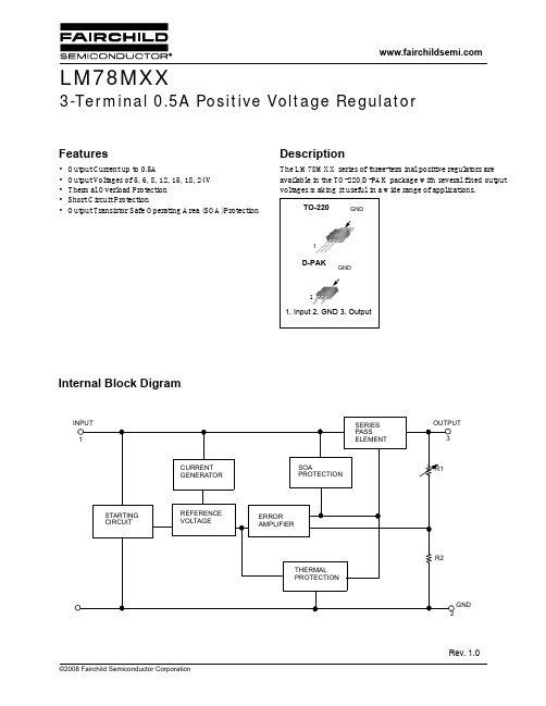
Rev. 1.0Features•Output Current up to 0.5A•Output V oltages of 5, 6, 8, 12, 15, 18, 24V •Thermal Overload Protection •Short Circuit Protection•Output Transistor Safe Operating Area (SOA)ProtectionDescriptionThe LM78MXX series of three-terminal positive regulators are available in the TO-220/D-PAK package with several fixed output voltages making it useful in a wide range of applications.TO-220D-PAK1. Input2. GND3. Output11GNDGNDInternal Block DigramOUTPUT3R1R2GND 21INPUT SERIES PASSELEMENTSOAPROTECTIONCURRENT GENERATOR STARTING CIRCUITREFERENCE VOLTAGEERROR AMPLIFIERTHERMAL PROTECTIONLM 78MXX3-Terminal 0.5A Positive Voltage RegulatorLM78MXXAbsolute Maximum RatingsNote:1. Thermal resistance test boardSize: 76.2mm * 114.3mm * 1.6mm(1S0P)JEDEC standard: JESD51-3, JESD51-72. Assume no ambient airflowElectrical Characteristics (LM78M05)(Refer to the test circuits, 0 < T J < +125°C, I O =350mA, V I =10V, unless otherwise specified, C I = 0.33µF, C O =0.1µF)Note:3. Load and line regulation are specified at constant junction temperature. Change in V o due to heating effects must be takeninto account separately. Pulse testing with low duty is used.ParameterSymbol Value Unit Input Voltage (for V O = 5V to 18V)(for V O = 24V)V I V I 3540V V Thermal Resistance Junction-Case (Note1)TO-220 (Tc = +25°C)R θJC 2.5°C/W Thermal Resistance Junction-Air (Note1, 2)TO-220 (Ta = +25°C)D-PAK (Ta = +25°C)R θJA 6692°C/W Operating Junction Temperature Range T OPR 0 ~ +150°C Storage Temperature RangeT STG-65 ~ +150°CParameter Symbol ConditionsMin.Typ.Max.UnitOutput VoltageV OT J = +25°C 4.85 5.2V I O = 5mA to 350mA V I = 7V to 20V 4.755 5.25Line Regulation (Note3)∆V O I O = 200mA T J =+25°CV I = 7V to 25V --100mV V I = 8V to 25V--50Load Regulation (Note3)∆V O I O = 5mA to 0.5A, T J =+25°C --100mV I O = 5mA to 200mA, T J =+25 °C --50Quiescent Current I Q T J =+25°C- 4.0 6.0mAQuiescent Current Change∆I Q I O = 5mA to 350mA --0.5mA I O = 200mA V I = 8V to 25V --0.8Output Voltage Drift ∆V/∆T I O = 5mAT J = 0 to +125°C --0.5-mV/°COutput Noise Voltage V N f = 10Hz to 100kHz -40-µV/VoRipple Rejection RR f = 120Hz, I O = 300mA V I = 8V to 18V, T J =+25 °C -80-dB Dropout Voltage V D T J =+25°C, I O = 500mA -2-V Short Circuit Current I SC T J =+25°C, V I = 35V -300-mA Peak CurrentI PKT J =+25°C-700-mALM78MXXElectrical Characteristics (LM 78M06) (Continued)(Refer to the test circuits, 0 < T J < +125°C, I O =350mA, V I =11V, unless otherwise specified, C I =0.33µF, C O =0.1µF)Note:1. Load and line regulation are specified at constant junction temperature. Change in V o due to heating effects must be takeninto account separately. Pulse testing with low duty is used.Parameter Symbol ConditionsMin.Typ.Max.UnitOutput VoltageV OT J = +25°C 5.756 6.25V I O = 5mA to 350mA V I = 8V to 21V 5.76 6.3Line Regulation (Note1)∆V O I O = 200mA T J = +25°CV I = 8V to 25V --100mV V I = 9V to 25V--50Load Regulation (Note1)∆V O I O = 5mA to 0.5A, T J = +25°C --120mV I O = 5mA to 200mA, T J = +25°C --60Quiescent Current I Q T J = +25°C - 4.0 6.0mAQuiescent Current Change∆I Q I O = 5mA to 350mA --0.5mA I O = 200mA V I = 9V to 25V --0.8Output Voltage Drift ∆V/∆T I O = 5mAT J = 0 to +125°C --0.5-mV/°COutput Noise Voltage V N f = 10Hz to 100kHz -45-µV/VoRipple Rejection RR f = 120Hz, I O = 300mA V I = 9V to 19V, T J =+25 °C -80-dB Dropout Voltage V D T J =+25°C, I O = 500mA -2-V Short Circuit Current I SC T J = +25°C, V I = 35V -300-mA Peak CurrentI PKT J =+25°C-700-mALM78MXXElectrical Characteristics (LM 78M08) (Continued)(Refer to the test circuits, 0 < T J < +125°C, I O =350mA, V I =14V, unless otherwise specified, C I = 0.33µF, C O =0.1µF)Note:1. Load and line regulation are specified at constant junction temperature. Change in V O due to heating effects must be takeninto account separately. Pulse testing with low duty is used.Parameter SymbolConditionsMin.Typ.Max.UnitOutput VoltageV OT J =+25°C7.788.3V I O = 5mA to 350mA V I = 10.5V to 23V 7.688.4Line Regulation (Note1)∆V O I O = 200mA T J =+25°CV I = 10.5V to 25V --100mV V I = 11V to 25V --50Load Regulation (Note1)∆V O I O = 5mA to 0.5A, T J =+25°C --160mV I O = 5mA to 200mA, T J =+25°C --80Quiescent Current I Q T J = +25°C - 4.0 6.0mAQuiescent Current Change∆I Q I O = 5mA to 350mA --0.5mA I O = 200mAV I = 10.5V to 25V --0.8Output Voltage Drift RR I O = 5mAT J = 0 to +125°C -−0.5-mV/°COutput Noise Voltage V N f = 10Hz to 100kHz-52-µV/VoRipple Rejection RR f = 120Hz, I O = 300mAV I = 11.5V to 21.5V, T J =+25 °C -80-dB Dropout Voltage V D T J = +25°C, I O = 500mA -2-V Short Circuit Current I SC T J = +25°C, V I = 35V -300-mA Peak CurrentI PKT J = +25°C-700-mA(Refer to the test circuits, 0 < T J < +125°C, I O =350mA, V I =19V, unless otherwise specified, C I =0.33µF, C O =0.1µF)Note:1. Load and line regulation are specified at constant junction temperature. Change in V o due to heating effects must be takeninto account separately. Pulse testing with low duty is used.Parameter SymbolConditionsMin.Typ.Max.UnitOutput VoltageV OT J = +25°C11.51212.5V I O = 5mA to 350mA V I = 14.5V to 27V 11.41212.6Line Regulation (Note1)∆V O I O = 200mA T J = +25°CV I = 14.5V to 30V --100mV V I = 16V to 30V --50Load Regulation (Note1)∆V O I O = 5mA to 0.5A, T J = +25°C --240mV I O = 5mA to 200mA, T J = +25°C --120Quiescent Current I Q T J =+25°C- 4.1 6.0mAQuiescent Current Change∆I Q I O = 5mA to 350mA --0.5mA I O = 200mAV I = 14.5V to 30V --0.8Output Voltage Drift ∆V/∆T I O = 5mAT J = 0 to +125°C --0.5-mV/°COutput Noise Voltage V N f = 10Hz to 100kHz-75-µV/VoRipple Rejection RR f = 120Hz, I O = 300mAV I = 15V to 25V, T J =+25 °C -80-dB Dropout Voltage V D T J =+25°C, I O = 500mA -2-V Short Circuit Current I SC T J = +25°C, V I = 35V -300-mA Peak CurrentI PKT J = +25°C-700-mA(Refer to the test circuits, 0 < T J < +125°C, I O =350mA, V I =23V, unless otherwise specified, C I =0.33µF, C O =0.1µF)Note:1. Load and line regulation are specified at constant junction temperature. Change in V O due to heating effects must be takeninto account separately. Pulse testing with low duty is used.Parameter Symbol ConditionsMin.Typ.Max.UnitOutput VoltageV OT J = +25°C 14.41515.6V I O = 5mA to 350mA V I = 17.5V to 30V 14.251515.75Line Regulation (Note1)∆V O I O = 200mA T J =+25°CV I = 17.5V to 30V --100mV V I = 20V to 30V--50Load Regulation (Note1)∆V O I O = 5mA to 0.5A, T J =+25°C --300mV I O = 5mA to 200mA, T J =+25°C --150Quiescent Current I Q T J = +25°C - 4.1 6.0mAQuiescent Current Change∆I Q I O = 5mA to 350mA --0.5mA I O = 200mAV I = 17.5V to 30V --0.8Output Voltage Drift ∆V/∆T I O = 5mAT J = 0 to +125°C --1-mV/°COutput Noise Voltage V N f = 10Hz to 100kHz-100-µV/VoRipple Rejection RR f = 120Hz, I O = 300mAV I = 18.5V to 28.5V, T J =+25 °C -70-dB Dropout Voltage V D T J =+25°C, I O = 500mA -2-V Short Circuit Current I SC T J = +25°C, V I = 35V -300-mA Peak CurrentI PKT J = +25°C-700-mALM78MXXElectrical Characteristics (LM 78M18) (Continued)(Refer to the test circuits, 0 < T J < +125°C, I O =350mA, V I =26V, unless otherwise specified, C I =0.33µF, C O =0.1µF)Note:1. Load and line regulation are specified at constant junction temperature. Change in V O due to heating effects must be takeninto account separately. Pulse testing with low duty is used.Parameter SymbolConditionsMin.Typ.Max.UnitOutput VoltageV OT J = +25°C17.31818.7V I O = 5mA to 350mA V I = 20.5V to 33V 17.11818.9Line Regulation (Note1)∆V O I O = 200mA T J = +25°CV I = 21V to 33V --100mV V I = 24V to 33V --50Load Regulation (Note1)∆V ΟI O = 5mA to 0.5A, T J = +25°C --360mV I O = 5mA to 200mA, T J = +25°C --180Quiescent Current I Q T J = +25°C - 4.2 6.0mAQuiescent Current Change ∆I Q I O = 5mA to 350mA --0.5mA I O = 200mA V I = 21V to 33V--0.8Output Voltage Drift ∆V/∆T I O = 5mAT J = 0 to 125°C --1.1-mV/°C Output Noise Voltage V N f = 10Hz to 100kHz-100-µV/Vo Ripple Rejection RR f = 120Hz, I O = 300mA , V I = 22V to 32V T J =+25 °C-70-dB Dropout Voltage V D T J = +25°C, I O = 500mA -2-V Short Circuit Current I SC T J = +25°C, V I = 35V -300-mA Peak CurrentI PKT J = +25°C-700-mAElectrical Characteristics (LM 78M24) (Continued)(Refer to the test circuits, 0 < T J < +125°C, I O =350mA, V I =33V, unless otherwise specified, C I =0.33µF, C O =0.1µF)Note:1. Load and line regulation are specified at constant junction temperature. Change in V O due to heating effects must be takeninto account separately. Pulse testing with low duty is used.Parameter Symbol ConditionsMin.Typ.Max.UnitOutput VoltageV OT J =+25°C 232425V I O = 5mA to 350mA V I = 27V to 38V22.82425.2Line Regulation (Note1)∆V O I O = 200mA T J =+25°C V I = 27V to 38V --100mV V I = 28V to 38V --50Load Regulation (Note1)∆V O I O = 5mA to 0.5A, T J =+25°C --480mV I O = 5mA to 200mA, T J =+25°C --240Quiescent CurrentI QT J = +25°C - 4.2 6.0mAQuiescent Current Change∆I Q I O = 5mA to 350mA--0.5mA I O = 200mA V I = 27V to 38V --0.8Output Voltage Drift ∆V/∆T I O = 5mAT J = 0 to +125°C --1.2-mV/°COutput Noise Voltage V N f = 10Hz to 100kHz-170-µV/VoRipple Rejection RR f = 120Hz, I O = 300mAV I = 28V to 38V, T J =+25 °C -70-dB Dropout Voltage V D T J = +25°C, I O = 500mA -2-V Short Circuit Current I SC T J = +25°C, V I = 35V -300-mA Peak CurrentI PKT J = +25°C-700-mATypical ApplicationsFigure 1.Fixed Output RegulatorFigure 2.Constant Current RegulatorNotes:1.To specify an output voltage, substitute voltage value for "XX"2.Although no output capacitor is needed for stability, it does improve transient response.3.C I is required if regulator is located an appreciable distance from power Supply filterFigure 3.Circuit for Increasing Output Voltage0.1µFC OC I0.3µFV OV ILM78MXX1320.1µFC OC I0.33µFI OV ILM78MXX132VXXI O R 1I O = R 1 +I OVxx 0.1µFC OC I0.33µFI OV ILM78MXX132V XXV OR 1R 2I R1 ≥ 5I OV O = V XX (1+R 2/R 1) +I O R 2LM78MXXFigure 4.Adjustable Output Regulator (7 to 30V)Figure 5.0.5 to 10V Regulator0.1µFC OC I0.33µFV OV ILM78M0513210k Ω32476LM7410.1µFC2C10.33µFV OV ILM78M0513210k Ω32476LM741R3R1VXXR4R5910Ω9.1k Ω13V < V I < 25V-7 < -VI < 17V_+VO = VxxR 1R 411Mechanical DimensionsPackageDimensions in millimeters4.50 ±0.209.90 ±0.201.52 ±0.100.80 ±0.102.40 ±0.2010.00 ±0.201.27 ±0.10ø3.60 ±0.10(8.70)2.80 ±0.1015.90 ±0.2010.08 ±0.3018.95M A X .(1.70)(3.70)(3.00)(1.46)(1.00)(45°)9.20 ±0.2013.08 ±0.201.30 ±0.101.30+0.10–0.050.50+0.10–0.052.54TYP [2.54 ±0.20]2.54TYP [2.54 ±0.20]TO-220Mechanical Dimensions (Continued)PackageDimensions in millimetersD-PAK12Ordering Information1311/12/02 0.0m 001Stock#DSxxxxxxxx2008 Fairchild Semiconductor CorporationLIFE SUPPORT POLICYFAIRCHILD’S PRODUCTS ARE NOT AUTHORIZED FOR USE AS CRITICAL COMPONENTS IN LIFE SUPPORT DEVICES OR SYSTEMS WITHOUT THE EXPRESS WRITTEN APPROVAL OF THE PRESIDENT OF FAIRCHILD SEMICONDUCTOR CORPORATION. As used herein:1.Life support devices or systems are devices or systemswhich, (a) are intended for surgical implant into the body, or (b) support or sustain life, and (c) whose failure to perform when properly used in accordance with instructions for use provided in the labeling, can bereasonably expected to result in a significant injury of the user.2. A critical component in any component of a life supportdevice or system whose failure to perform can bereasonably expected to cause the failure of the life support device or system, or to affect its safety or effectiveness.DISCLAIMERFAIRCHILD SEMICONDUCTOR RESERVES THE RIGHT TO MAKE CHANGES WITHOUT FURTHER NOTICE TO ANY PRODUCTS HEREIN TO IMPROVE RELIABILITY, FUNCTION OR DESIGN. FAIRCHILD DOES NOT ASSUME ANYLIABILITY ARISING OUT OF THE APPLICATION OR USE OF ANY PRODUCT OR CIRCUIT DESCRIBED HEREIN; NEITHER DOES IT CONVEY ANY LICENSE UNDER ITS PATENT RIGHTS, NOR THE RIGHTS OF OTHERS.。
L78L12中文资料

L78L00SERIESPOSITIVE VOLTAGE REGULATORS®November 1998s OUTPUT CURRENT UP TO 100mAsOUTPUT VOLTAGESOF 3.3;5;6;8;9;12;15;18;24Vs THERMAL OVERLOAD PROTECTION s SHORT CIRCUIT PROTECTIONsNO EXTERNAL COMPONENTS ARE REQUIREDsAVAILABLEIN EITHER ±5%(AC)OR ±10%(C)SELECTIONDESCRIPTIONThe L78L00series of three-terminal positive regulators employ internal current limiting and thermal shutdown,making them essentially indestructible.If adequate heatsink is provided,they can deliver up to 100mA output current.They are intended as fixed voltage regulators in a wide range of applications including local or on-card regulation for elimination of noise and distribution problems associated with single-point regulation.In addition,they can be used with power pass elements to make high-current voltage regulators.The L78L00series used as Zener diode/resistor combination replacement,offers an effectiveBLOCK DIAGRAMSO-8TO-92output impedance improvement of typically two orders of magnetude,along with lower quiescent current and lower noise.SOT-891/19ABSOLUTE MAXIMUM RATINGSymbol ParameterValue Unit V iDC Input VoltageV o =3.3V to 9V 30V V o =12V to 15V 35V V o =18V to 24V40V I o Output Current 100mA P tot Power DissipationInternally limited (*)T st g Storage Temperature Range-40to 150o C T opOperating Junction Temperature RangeFor L78L00C,L78L00AC For L78L00AB0to 125-40to 125o C oC(*)Our SO-8package used for Voltage Regulators is modified internally to have pins 2,3,6and 7electrically commoned to the die attach flag.This particular frame decreases the total thermal resistance of the package and increases its ability to dissipate power when an appropriate area of copper on the printed circuit board is available for heatsinking.The external dimensions are the same as for the standard SO-8TEST CIRCUITSTHERMAL DATASymbolParameterSO-8TO-92SOT-89UnitR thj-ca se R thj-amb Thermal Resistance Junction-case Max Thermal Resistance Junction-ambientMax2055(*)20012o C/W oC/W(*)Considering 6cm 2of copper Board heat-sinkL78L002/19CONNECTION DIAGRAM AND ORDERING NUMBERS(top view)ORDERING NUMBERSType SO-8TO-92SOT-89Output VoltageL78L33AC L78L33AB L78L05C L78L05AC L78L05AB L78L06C L78L06AC L78L06AB L78L08C L78L08AC L78L08AB L78L09C L78L09AC L78L09AB L78L12C L78L12AC L78L12AB L78L15C L78L15AC L78L15AB L78L18C L78L18AC L78L18AB L78L24C L78L24AC L78L24ABL78L33ACDL78L33ABDL78L05CDL78L05ACDL78L05ABDL78L06CDL78L06ACDL78L06ABDL78L08CDL78L08ACDL78L08ABDL78L09CDL78L09ACDL78L09ABDL78L12CDL78L12ACDL78L12ABDL78L15CDL78L15ACDL78L15ABDL78L18CDL78L18ACDL78L18ABDL78L24CDL78L24ACDL78L24ABDL78L33ACZL78L33ABZL78L05CZL78L05ACZL78L05ABZL78L06CZL78L06ACZL78L06ABZL78L08CZL78L08ACZL78L08ABZL78L09CZL78L09ACZL78L09ABZL78L12CZL78L12ACZL78L12ABZL78L15CZL78L15ACZL78L15ABZL78L18CZL78L18ACZL78L18ABZL78L24CZL78L24ACZL78L24ABZL78L33ACUL78L33ABUL78L05ACUL78L05ABUL78L06ACUL78L06ABUL78L08ACUL78L08ABUL78L09ACUL78L09ABUL78L12ACUL78L12ABUL78L15ACUL78L15ABUL78L18ACUL78L18ABUL78L24ACUL78L24ABU3.3V3.3V5V5V5V6V6V6V8V8V8V9V9V9V12V12V12V15V15V15V18V18V18V24V24V24VSO-8TO-92pin1=V OUTpin2=GNDpin3=V INBOTTOM VIEWSOT-89L78L003/19ELECTRICAL CHARACTERISTICS FOR L78L05(refer to the test circuits,T j=0to125o C,V i=10V,I o=40mA,C i=0.33µF,C o=0.1µF unless otherwise specified)Symbol Parameter Test Conditions Min.Typ.Max.Unit V o Output Voltage T j=25o C 4.65 5.4VV o Output Voltage I o=1to40mA V i=7to20VI o=1to70mA V i=10V 4.54.55.55.5VV∆V o Line Regulation V i=7to20V T j=25o CV i=8to20V T j=25o C 200150mVmV∆V o Load Regulation I o=1to100mA T j=25o CI o=1to40mA T j=25o C 6030mVmVI d Quiescent Current T j=25o CT j=125o C65.5mAmA∆I d Quiescent Current Change I o=1to40mA0.2mA ∆I d Quiescent Current Change V i=8to20V 1.5mA eN Output Noise Voltage B=10Hz to100KHz T j=25o C40µV SVR Supply Voltage Rejection I o=40mA f=120Hz T j=25o CV i=8to18V4049dB V d Dropout Voltage 1.7VELECTRICAL CHARACTERISTICS FOR L78L06(refer to the test circuits,T j=0to125o C,V i=12V,I o=40mA,C i=0.33µF,C o=0.1µF unless otherwise specified)Symbol Parameter Test Conditions Min.Typ.Max.Unit V o Output Voltage T j=25o C 5.526 6.48VV o Output Voltage I o=1to40mA V i=8.5to20VI o=1to70mA V i=12V 5.45.46.66.6VV∆V o Line Regulation V i=8.5to20V T j=25o CV i=9to20V T j=25o C 200150mVmV∆V o Load Regulation I o=1to100mA T j=25o CI o=1to40mA T j=25o C 6030mVmVI d Quiescent Current T j=25o CT j=125o C65.5mAmA∆I d Quiescent Current Change I o=1to40mA0.2mA ∆I d Quiescent Current Change V i=8to20V 1.5mA eN Output Noise Voltage B=10Hz to100KHz T j=25o C50µV SVR Supply Voltage Rejection I o=40mA f=120Hz T j=25o CV i=9to20V3846dB V d Dropout Voltage 1.7V L78L004/19ELECTRICAL CHARACTERISTICS FOR L78L08(refer to the test circuits,T j=0to125o C,V i=14V,I o=40mA,C i=0.33µF,C o=0.1µF unless otherwise specified)Symbol Parameter Test Conditions Min.Typ.Max.Unit V o Output Voltage T j=25o C7.3688.64VV o Output Voltage I o=1to40mA V i=10.5to23VI o=1to70mA V i=14V 7.27.28.88.8VV∆V o Line Regulation V i=10.5to23V T j=25o CV i=11to23V T j=25o C 200150mVmV∆V o Load Regulation I o=1to100mA T j=25o CI o=1to40mA T j=25o C 8040mVmVI d Quiescent Current T j=25o CT j=125o C65.5mAmA∆I d Quiescent Current Change I o=1to40mA0.2mA ∆I d Quiescent Current Change V i=11to23V 1.5mA eN Output Noise Voltage B=10Hz to100KHz T j=25o C60µV SVR Supply Voltage Rejection I o=40mA f=120Hz T j=25o CV i=12to23V3645dB V d Dropout Voltage 1.7VELECTRICAL CHARACTERISTICS FOR L78L09(refer to the test circuits,T j=0to125o C,V i=15V,I o=40mA,C i=0.33µF,C o=0.1µF unless otherwise specified)Symbol Parameter Test Conditions Min.Typ.Max.Unit V o Output Voltage T j=25o C8.2899.72VV o Output Voltage I o=1to40mA V i=11.5to23VI o=1to70mA V i=15V 8.18.19.99.9VV∆V o Line Regulation V i=11.5to23V T j=25o CV i=12to23V T j=25o C 250200mVmV∆V o Load Regulation I o=1to100mA T j=25o CI o=1to40mA T j=25o C 8040mVmVI d Quiescent Current T j=25o CT j=125o C65.5mAmA∆I d Quiescent Current Change I o=1to40mA0.2mA∆I d Quiescent Current Change V i=12to23V 1.5mA eN Output Noise Voltage B=10Hz to100KHz T j=25o C70µV SVR Supply Voltage Rejection I o=40mA f=120Hz T j=25o CV i=12to23V3644dBV d Dropout Voltage 1.7VL78L005/19ELECTRICAL CHARACTERISTICS FOR L78L12(refer to the test circuits,T j=0to125o C,V i=19V,I o=40mA,C i=0.33µF,C o=0.1µF unless otherwise specified)Symbol Parameter Test Conditions Min.Typ.Max.Unit V o Output Voltage T j=25o C11.11212.9VV o Output Voltage I o=1to40mA V i=14.5to27VI o=1to70mA V i=19V 10.810.813.213.2VV∆V o Line Regulation V i=14.5to27V T j=25o CV i=16to27V T j=25o C 250200mVmV∆V o Load Regulation I o=1to100mA T j=25o CI o=1to40mA T j=25o C 10050mVmVI d Quiescent Current T j=25o CT j=125o C 6.56mAmA∆I d Quiescent Current Change I o=1to40mA0.2mA ∆I d Quiescent Current Change V i=16to27V 1.5mA eN Output Noise Voltage B=10Hz to100KHz T j=25o C80µV SVR Supply Voltage Rejection I o=40mA f=120Hz T j=25o CV i=15to25V3642dB V d Dropout Voltage 1.7VELECTRICAL CHARACTERISTICS FOR L78L15(refer to the test circuits,T j=0to125o C,V i=23V,I o=40mA,C i=0.33µF,C o=0.1µF unless otherwise specified)Symbol Parameter Test Conditions Min.Typ.Max.Unit V o Output Voltage T j=25o C13.81516.2VV o Output Voltage I o=1to40mA V i=17.5to30VI o=1to70mA V i=23V 13.513.516.516.5VV∆V o Line Regulation V i=17.5to30V T j=25o CV i=20to30V T j=25o C 300250mVmV∆V o Load Regulation I o=1to100mA T j=25o CI o=1to40mA T j=25o C 15075mVmVI d Quiescent Current T j=25o CT j=125o C 6.56mAmA∆I d Quiescent Current Change I o=1to40mA0.2mA ∆I d Quiescent Current Change V i=20to30V 1.5mA eN Output Noise Voltage B=10Hz to100KHz T j=25o C90µV SVR Supply Voltage Rejection I o=40mA f=120Hz T j=25o CV i=18.5to28.5V3339dB V d Dropout Voltage 1.7V L78L006/19ELECTRICAL CHARACTERISTICS FOR L78L18(refer to the test circuits,T j=0to125o C,V i=27V,I o=40mA,C i=0.33µF,C o=0.1µF unless otherwise specified)Symbol Parameter Test Conditions Min.Typ.Max.Unit V o Output Voltage T j=25o C16.61819.4VV o Output Voltage I o=1to40mA V i=22to33VI o=1to70mA V i=27V 16.216.219.819.8VV∆V o Line Regulation V i=22to33V T j=25o CV i=22to33V T j=25o C 320270mVmV∆V o Load Regulation I o=1to100mA T j=25o CI o=1to40mA T j=25o C 17085mVmVI d Quiescent Current T j=25o CT j=125o C 6.56mAmA∆I d Quiescent Current Change I o=1to40mA0.2mA ∆I d Quiescent Current Change V i=23to33V 1.5mA eN Output Noise Voltage B=10Hz to100KHz T j=25o C120µV SVR Supply Voltage Rejection I o=40mA f=120Hz T j=25o CV i=23to33V3238dB V d Dropout Voltage 1.7VELECTRICAL CHARACTERISTICS FOR L78L24(refer to the test circuits,T j=0to125o C,V i=33V,I o=40mA,C i=0.33µF,C o=0.1µF unless otherwise specified)Symbol Parameter Test Conditions Min.Typ.Max.Unit V o Output Voltage T j=25o C22.12425.9VV o Output Voltage I o=1to40mA V i=27to38VI o=1to70mA V i=33V 21.621.626.426.4VV∆V o Line Regulation V i=27to38V T j=25o CV i=28to38V T j=25o C 350300mVmV∆V o Load Regulation I o=1to100mA T j=25o CI o=1to40mA T j=25o C 200100mVmVI d Quiescent Current T j=25o CT j=125o C 6.56mAmA∆I d Quiescent Current Change I o=1to40mA0.2mA∆I d Quiescent Current Change V i=28to38V 1.5mA eN Output Noise Voltage B=10Hz to100KHz T j=25o C200µV SVR Supply Voltage Rejection I o=40mA f=120Hz T j=25o CV i=29to35V3037dBV d Dropout Voltage 1.7VL78L007/19ELECTRICAL CHARACTERISTICS FOR L78L33AB AND L78L33AC(refer to the test circuits,V i=8.3V,I o=40mA,C i=0.33µF,C o=0.1µF,T j=0to125o C for L78L33AC,T j=-40to125o C for L78L33AB,unless otherwise specified)Symbol Parameter Test Conditions Min.Typ.Max.Unit V o Output Voltage T j=25o C 3.168 3.3 3.432VV o Output Voltage I o=1to40mA V i=5.3to20VI o=1to70mA V i=8.3V 3.1353.1353.4653.465VV∆V o Line Regulation V i=5.3to20V T j=25o CV i=6.3to20V T j=25o C 150100mVmV∆V o Load Regulation I o=1to100mA T j=25o CI o=1to40mA T j=25o C 6030mVmVI d Quiescent Current T j=25o CT j=125o C65.5mAmA∆I d Quiescent Current Change I o=1to40mA0.1mA ∆I d Quiescent Current Change V i=6.3to20V 1.5mA eN Output Noise Voltage B=10Hz to100KHz T j=25o C40µV SVR Supply Voltage Rejection I o=40mA f=120Hz T j=25o CV i=6.3to16.3V4149dB V d Dropout Voltage 1.7VELECTRICAL CHARACTERISTICS FOR L78L05AB AND L78L05AC(refer to the test circuits,V i=10V,I o=40mA,C i=0.33µF,C o=0.1µF,T j=0to125o C for L78L05AC,T j=-40to125o C for L78L05AB,unless otherwise specified)Symbol Parameter Test Conditions Min.Typ.Max.Unit V o Output Voltage T j=25o C 4.85 5.2VV o Output Voltage I o=1to40mA V i=7to20VI o=1to70mA V i=10V 4.754.755.255.25VV∆V o Line Regulation V i=7to20V T j=25o CV i=8to20V T j=25o C 150100mVmV∆V o Load Regulation I o=1to100mA T j=25o CI o=1to40mA T j=25o C 6030mVmVI d Quiescent Current T j=25o CT j=125o C65.5mAmA∆I d Quiescent Current Change I o=1to40mA0.1mA ∆I d Quiescent Current Change V i=8to20V 1.5mA eN Output Noise Voltage B=10Hz to100KHz T j=25o C40µV SVR Supply Voltage Rejection I o=40mA f=120Hz T j=25o CV i=8to18V4149dB V d Dropout Voltage 1.7V L78L008/19ELECTRICAL CHARACTERISTICS FOR L78L06AB AND L78L06AC(refer to the test circuits,V i=12V,I o=40mA,C i=0.33µF,C o=0.1µF,T j=0to125o C for L78L06AC,T j=-40to125o C for L78L06AB,unless otherwise specified)Symbol Parameter Test Conditions Min.Typ.Max.Unit V o Output Voltage T j=25o C 5.766 6.24VV o Output Voltage I o=1to40mA V i=8.5to20VI o=1to70mA V i=12V 5.75.76.36.3VV∆V o Line Regulation V i=8.5to20V T j=25o CV i=9to20V T j=25o C 150100mVmV∆V o Load Regulation I o=1to100mA T j=25o CI o=1to40mA T j=25o C 6030mVmVI d Quiescent Current T j=25o CT j=125o C65.5mAmA∆I d Quiescent Current Change I o=1to40mA0.1mA ∆I d Quiescent Current Change V i=9to20V 1.5mA eN Output Noise Voltage B=10Hz to100KHz T j=25o C50µV SVR Supply Voltage Rejection I o=40mA f=120Hz T j=25o CV i=9to20V3946dB V d Dropout Voltage 1.7VELECTRICAL CHARACTERISTICS FOR L78L08AB AND L78L08AC(refer to the test circuits,V i=14V,I o=40mA,C i=0.33µF,C o=0.1µF,T j=0to125o C for L78L08AC,T j=-40to125o C for L78L08AB,unless otherwise specified)Symbol Parameter Test Conditions Min.Typ.Max.Unit V o Output Voltage T j=25o C7.6888.32VV o Output Voltage I o=1to40mA V i=10.5to23VI o=1to70mA V i=14V 7.67.68.48.4VV∆V o Line Regulation V i=10.5to23V T j=25o CV i=11to23V T j=25o C 175125mVmV∆V o Load Regulation I o=1to100mA T j=25o CI o=1to40mA T j=25o C 8040mVmVI d Quiescent Current T j=25o CT j=125o C65.5mAmA∆I d Quiescent Current Change I o=1to40mA0.1mA∆I d Quiescent Current Change V i=11to23V 1.5mA eN Output Noise Voltage B=10Hz to100KHz T j=25o C60µV SVR Supply Voltage Rejection I o=40mA f=120Hz T j=25o CV i=12to23V3745dBV d Dropout Voltage 1.7VL78L009/19ELECTRICAL CHARACTERISTICS FOR L78L09AB AND L78L09AC(refer to the test circuits,V i=15V,I o=40mA,C i=0.33µF,C o=0.1µF,T j=0to125o C for L78L09AC,T j=-40to125o C for L78L09AB,unless otherwise specified)Symbol Parameter Test Conditions Min.Typ.Max.Unit V o Output Voltage T j=25o C8.6499.36VV o Output Voltage I o=1to40mA V i=11.5to23VI o=1to70mA V i=15V 8.558.559.459.45VV∆V o Line Regulation V i=11.5to23V T j=25o CV i=12to23V T j=25o C 225150mVmV∆V o Load Regulation I o=1to100mA T j=25o CI o=1to40mA T j=25o C 8040mVmVI d Quiescent Current T j=25o CT j=125o C65.5mAmA∆I d Quiescent Current Change I o=1to40mA0.1mA ∆I d Quiescent Current Change V i=12to23V 1.5mA eN Output Noise Voltage B=10Hz to100KHz T j=25o C70µV SVR Supply Voltage Rejection I o=40mA f=120Hz T j=25o CV i=12to23V3744dB V d Dropout Voltage 1.7VELECTRICAL CHARACTERISTICS FOR L78L12AB AND L78L12AC(refer to the test circuits,V i=19V,I o=40mA,C i=0.33µF,C o=0.1µF,T j=0to125o C for L78L12AC,T j=-40to125o C for L78L12AB,unless otherwise specified)Symbol Parameter Test Conditions Min.Typ.Max.Unit V o Output Voltage T j=25o C11.51212.5VV o Output Voltage I o=1to40mA V i=14.5to27VI o=1to70mA V i=19V 11.411.412.612.6VV∆V o Line Regulation V i=14.5to27V T j=25o CV i=16to27V T j=25o C 250200mVmV∆V o Load Regulation I o=1to100mA T j=25o CI o=1to40mA T j=25o C 10050mVmVI d Quiescent Current T j=25o CT j=125o C 6.56mAmA∆I d Quiescent Current Change I o=1to40mA0.1mA ∆I d Quiescent Current Change V i=16to27V 1.5mA eN Output Noise Voltage B=10Hz to100KHz T j=25o C80µV SVR Supply Voltage Rejection I o=40mA f=120Hz T j=25o CV i=15to25V3742dB V d Dropout Voltage 1.7V L78L0010/19ELECTRICAL CHARACTERISTICS FOR L78L15AB AND L78L15AC(refer to the test circuits,V i=23V,I o=40mA,C i=0.33µF,C o=0.1µF,T j=0to125o C for L78L15AC,T j=-40to125o C for L78L15AB,unless otherwise specified)Symbol Parameter Test Conditions Min.Typ.Max.Unit V o Output Voltage T j=25o C14.41515.6VV o Output Voltage I o=1to40mA V i=17.5to30VI o=1to70mA V i=23V 14.2514.2515.7515.75VV∆V o Line Regulation V i=17.5to30V T j=25o CV i=20to30V T j=25o C 300250mVmV∆V o Load Regulation I o=1to100mA T j=25o CI o=1to40mA T j=25o C 15075mVmVI d Quiescent Current T j=25o CT j=125o C 6.56mAmA∆I d Quiescent Current Change I o=1to40mA0.1mA ∆I d Quiescent Current Change V i=20to30V 1.5mA eN Output Noise Voltage B=10Hz to100KHz T j=25o C90µV SVR Supply Voltage Rejection I o=40mA f=120Hz T j=25o CV i=18.5to28.5V3439dB V d Dropout Voltage 1.7VELECTRICAL CHARACTERISTICS FOR L78L18AB AND L78L18AC(refer to the test circuits,V i=27V,I o=40mA,C i=0.33µF,C o=0.1µF,T j=0to125o C for L78L18AC,T j=-40to125o C for L78L18AB,unless otherwise specified)Symbol Parameter Test Conditions Min.Typ.Max.Unit V o Output Voltage T j=25o C17.31818.7VV o Output Voltage I o=1to40mA V i=22to33VI o=1to70mA V i=27V 17.117.118.918.9VV∆V o Line Regulation V i=22to33V T j=25o CV i=22to33V T j=25o C 320270mVmV∆V o Load Regulation I o=1to100mA T j=25o CI o=1to40mA T j=25o C 17085mVmVI d Quiescent Current T j=25o CT j=125o C 6.56mAmA∆I d Quiescent Current Change I o=1to40mA0.1mA∆I d Quiescent Current Change V i=23to33V 1.5mA eN Output Noise Voltage B=10Hz to100KHz T j=25o C120µV SVR Supply Voltage Rejection I o=40mA f=120Hz T j=25o CV i=23to33V3338dBV d Dropout Voltage 1.7V11/19ELECTRICAL CHARACTERISTICS FOR L78L24AB AND L78L24AC(refer to the test circuits,V i=33V,I o=40mA,C i=0.33µF,C o=0.1µF,T j=0to125o C for L78L24AC,T j=-40to125o C for L78L24AB,unless otherwise specified)Symbol Parameter Test Conditions Min.Typ.Max.Unit V o Output Voltage T j=25o C232425VV o Output Voltage I o=1to40mA V i=27to38VI o=1to70mA V i=33V 22.822.825.225.2VV∆V o Line Regulation V i=27to38V T j=25o CV i=28to38V T j=25o C 350300mVmV∆V o Load Regulation I o=1to100mA T j=25o CI o=1to40mA T j=25o C 200100mVmVI d Quiescent Current T j=25o CT j=125o C 6.56mAmA∆I d Quiescent Current Change I o=1to40mA0.1mA ∆I d Quiescent Current Change V i=28to38V 1.5mA eN Output Noise Voltage B=10Hz to100KHz T j=25o C200µV SVR Supply Voltage Rejection I o=40mA f=120Hz T j=25o CV i=29to35V3137dB V d Dropout Voltage 1.7V12/19Figure3:L78L05/12/24Thermal Shutdown.Figure4:L78L05/12Quiescent Current vsOutput CurrentFigure5:L78L05Quiescent Current vs Input Voltage.Figure6:L78L05/12/24Output Characteristics.Figure1:L78L05/12Output Voltage vs AmbientTemperatureFigure2:L78L05/12/24Load Characteristics.13/19Figure7:L78L05/12/24Ripple Rejection.Figure8:L78L05Dropout Characteristics. Figure9:L78L00Series Short Circuit OutputCurrent.TYPICAL APPLICATIONS:Figure10:High Output Current Short Circuit Protected14/19Figure11:Output Boost Circuit.Figure12:Current Regulator.Figure13:Adjustable Output Regulator15/19SO-8MECHANICAL DATAmm inch DIM.MIN.TYP.MAX.MIN.TYP.MAX.A 1.750.068a10.10.250.0030.009 a2 1.650.064 a30.650.850.0250.033 b0.350.480.0130.018 b10.190.250.0070.010 C0.250.50.0100.019 c145(typ.)D 4.8 5.00.1880.196E 5.8 6.20.2280.244e 1.270.050e3 3.810.150F 3.8 4.00.140.157L0.4 1.270.0150.050 M0.60.023 S8(max.)0016023 16/19SOT-89MECHANICAL DATAmm milsDIM.MIN.TYP.MAX.MIN.TYP.MAX.A 1.4 1.655.163.0B0.440.5617.322.0B10.360.4814.218.9C0.350.4413.817.3C10.350.4413.817.3D 4.4 4.6173.2181.1D1 1.62 1.8363.872.0E 2.29 2.690.2102.4e 1.42 1.5755.961.8e1 2.92 3.07115.0120.9H 3.94 4.25155.1167.3L0.89 1.235.047.2P025H17/19TO-92MECHANICAL DATAmm inch DIM.MIN.TYP.MAX.MIN.TYP.MAX.A 4.58 5.330.1800.210B 4.45 5.20.1750.204C 3.2 4.20.1260.165D12.70.500E 1.270.050F0.40.510.0160.020 G0.350.1418/19Information furnished is believed to be accurate and reliable.However,STMicroelectronics assumes no responsibility for the consequence s of use of such information nor for any infringement of patents or other rights of third parties which may result from its use.No license is granted by implication or otherwise under any patent or patent rights of STMicroelectronics.Specification mentioned in this publication are subject to change without notice.This publication supersedes and replaces all information previously supplied.STMicroelectronics products are not authorized for use as critical components in life support devices or systems without express written approval of STMicroelectronics.The ST logo is a registered trademark of STMicroelectronics©1998STMicroelectronics–Printed in Italy–All Rights ReservedSTMicroelectronics GROUP OF COMPANIESAustralia-Brazil-Canada-China-France-Germany-Italy-Japan-Korea-Malaysia-Malta-Mexico-Morocco-The Netherlands-Singapore-Spain-Sweden-Switzerland-Taiwan-Thailand-United Kingdom-U.S.A..19/19。
LM78M15中文资料

LM341/LM78MXX Series3-Terminal Positive Voltage RegulatorsGeneral DescriptionThe LM341and LM78MXX series of three-terminal positive voltage regulators employ built-in current limiting,thermal shutdown,and safe-operating area protection which makes them virtually immune to damage from output overloads.With adequate heatsinking,they can deliver in excess of 0.5A output current.Typical applications would include local (on-card)regulators which can eliminate the noise and de-graded performance associated with single-point regulation.Featuresn Output current in excess of 0.5A n No external componentsn Internal thermal overload protection n Internal short circuit current-limitingn Output transistor safe-area compensationnAvailable in TO-220,TO-39,and TO-252D-PAK packagesn Output voltages of 5V,12V,and 15VConnection DiagramsTO-39Metal Can Package (H)DS010484-5Bottom ViewOrder Number LM78M05CH,LM78M12CH or LM78M15CHSee NS Package Number H03ATO-220Power Package (T)DS010484-6Top ViewOrder Number LM341T-5.0,LM341T-12,LM341T-15,LM78M05CT,LM78M12CT or LM78M15CTSee NS Package Number T03BTO-252DS010484-19Top ViewOrder Number LM78M05CDT See NS Package Number TD03BJuly 1999LM341/LM78MXX Series 3-Terminal Positive Voltage Regulators©1999National Semiconductor Corporation Absolute Maximum Ratings(Note1)If Military/Aerospace specified devices are required, please contact the National Semiconductor Sales Office/ Distributors for availability and specifications.Lead Temperature(Soldering,10seconds)TO-39Package(H)300˚C TO-220Package(T)260˚C Storage Temperature Range−65˚C to+150˚C Operating Junction TemperatureRange−40˚C to+125˚C Power Dissipation(Note2)Internally Limited Input Voltage5V≤V O≤15V35V ESD Susceptibility TBDElectrical CharacteristicsLimits in standard typeface are for T J=25˚C,and limits in boldface type apply over the−40˚C to+125˚C operating temperature range.Limits are guaranteed by production testing or correlation techniques using standard Statistical Quality Control(SQC) methods.LM341-5.0,LM78M05CUnless otherwise specified:V IN=10V,C IN=0.33µF,C O=0.1µFSymbol Parameter Conditions Min Typ Max Units V O Output Voltage I L=500mA 4.8 5.0 5.2V5mA≤I L≤500mA 4.75 5.0 5.25P D≤7.5W,7.5V≤V IN≤20VV R LINE Line Regulation7.2V≤V IN≤25V I L=100mA50mVI L=500mA100V R LOAD Load Regulation5mA≤I L≤500mA100I Q Quiescent Current I L=500mA410.0mA ∆I Q Quiescent Current Change5mA≤I L≤500mA0.57.5V≤V IN≤25V,I L=500mA 1.0V n Output Noise Voltage f=10Hz to100kHz40µVElectrical CharacteristicsLimits in standard typeface are for T J=25˚C,and limits in boldface type apply over the−40˚C to+125˚C operating temperature range.Limits are guaranteed by production testing or correlation techniques using standard Statistical Quality Control(SQC) methods.(Continued)LM341-12,LM78M12CUnless otherwise specified:V IN=19V,C IN=0.33µF,C O=0.1µFSymbol Parameter Conditions Min Typ Max UnitsV O Output Voltage I L=500mA11.51212.5V5mA≤I L≤500mA11.41212.6P D≤7.5W,14.8V≤V IN≤27VV R LINE Line Regulation14.5V≤V IN≤30V I L=100mA120mVI L=500mA240V R LOAD Load Regulation5mA≤I L≤500mA240I Q Quiescent Current I L=500mA410.0mA∆I Q Quiescent Current Change5mA≤I L≤500mA0.514.8V≤V IN≤30V,I L=500mA 1.0V n Output Noise Voltage f=10Hz to100kHz75µVRipple Rejection f=120Hz,I L=500mA69dBV IN Input Voltage Required I L=500mA17.6V to Maintain Line Regulation∆V O Long Term Stability I L=500mA60mV/khrs Note1:Absolute maximum ratings indicate limits beyond which damage to the component may occur.Electrical specifications do not apply when operating the de-vice outside of its rated operating conditions.Note2:The typical thermal resistance of the three package types is:T(TO-220)package:θ(JA)=60˚C/W,θ(JC)=5˚C/WH(TO-39)package:θ(JA)=120˚C/W,θ(JC)=18˚C/WDT(TO-252)package:θ(JA)=92˚C/W,θ(JC)=10˚C/W3Schematic DiagramDS010484-1 4Typical Performance CharacteristicsPeak Output CurrentDS010484-10Ripple RejectionDS010484-11Ripple RejectionDS010484-12Dropout VoltageDS010484-13Output Voltage(Normalizedto1V at T J=25˚C)DS010484-14Quiescent CurrentDS010484-15 5Typical Performance Characteristics(Continued)Design ConsiderationsThe LM78MXX/LM341XX fixed voltage regulator series has built-in thermal overload protection which prevents the de-vice from being damaged due to excessive junction tem-perature.The regulators also contain internal short-circuit protection which limits the maximum output current,and safe-area pro-tection for the pass transistor which reduces the short-circuit current as the voltage across the pass transistor is in-creased.Although the internal power dissipation is automatically lim-ited,the maximum junction temperature of the device must be kept below +125˚C in order to meet data sheet specifica-tions.An adequate heatsink should be provided to assure this limit is not exceeded under worst-case operating condi-tions (maximum input voltage and load current)if reliable performance is to be obtained).1.0Heatsink ConsiderationsWhen an integrated circuit operates with appreciable cur-rent,its junction temperature is elevated.It is important to quantify its thermal limits in order to achieve acceptable per-formance and reliability.This limit is determined by summing the individual parts consisting of a series of temperature rises from the semiconductor junction to the operating envi-ronment.A one-dimension steady-state model of conduction heat transfer is demonstrated in The heat generated at thedevice junction flows through the die to the die attach pad,through the lead frame to the surrounding case material,to the printed circuit board,and eventually to the ambient envi-ronment.Below is a list of variables that may affect the ther-mal resistance and in turn the need for a heatsink.R θJC (Component Variables)R θCA (Application Variables)Leadframe Size &Material Mounting Pad Size,Material,&LocationNo.of Conduction Pins Placement of Mounting Pad Die SizePCB Size &Material Die Attach MaterialTraces Length &WidthMolding Compound Size and MaterialAdjacent Heat Sources Volume of Air Air FlowAmbient Temperature Shape of Mounting PadQuiescent CurrentDS010484-16Output ImpedanceDS010484-17Line Transient Response DS010484-7Load Transient ResponseDS010484-86Design Considerations(Continued)The LM78MXX/LM341XX regulators have internal thermal shutdown to protect the device from over-heating.Under all possible operating conditions,the junction temperature of the LM78MXX/LM341XX must be within the range of 0˚C to 125˚C.A heatsink may be required depending on the maxi-mum power dissipation and maximum ambient temperature of the application.To determine if a heatsink is needed,the power dissipated by the regulator,P D ,must be calculated:I IN =I L +I GP D =(V IN −V OUT )I L +V IN I Gshows the voltages and currents which are present in the circuit.The next parameter which must be calculated is the maxi-mum allowable temperature rise,T R (max):θJA =TR (max)/P D If the maximum allowable value for θJA ˚C/w is found to be ≥60˚C/W for TO-220package or ≥92˚C/W for TO-252pack-age,no heatsink is needed since the package alone will dis-sipate enough heat to satisfy these requirements.If the cal-culated value for θJA fall below these limits,a heatsink is required.As a design aid,Table 1shows the value of the θJA of TO-252for different heatsink area.The copper patterns that we used to measure these θJA are shown at the end of the Application Note Section.reflects the same test results as what are in the Table 1shows the maximum allowable power dissipation vs.ambi-ent temperature for theTO-252device.shows the maximum allowable power dissipation vs.copper area (in 2)for the TO-252device.Please see AN1028for power enhancement techniques to be used with TO-252package.TABLE 1.θJA Different Heatsink AreaLayoutCopper AreaThermal Resistance Top Sice (in 2)*Bottom Side (in 2)(θJA ,˚C/W)TO-25210.0123010320.06608730.306040.5305450.7605261047700.284800.470900.6631000.857110157120.0660.06689130.1750.17572140.2840.28461150.3920.39255160.50.553*Tab of device attached to topside copperDS010484-23FIGURE 1.Cross-sectional view of Integrated Circuit Mounted on a printed circuit board.Note that the case temperature is measured at the point where the leadscontact with the mounting pad surface DS010484-24FIGURE 2.Power Dissipation Diagram7Design Considerations(Continued)Typical ApplicationDS010484-20FIGURE 3.θJA vs.2oz Copper Area for TO-252DS010484-22FIGURE 4.Maximum Allowable Power Dissipation vs.Ambient Temperature for TO-252DS010484-21FIGURE 5.Maximum Allowable Power Dissipation vs.2oz.Copper Area for TO-252DS010484-9*Required if regulator input is more than 4inches from input filter capacitor (or if no input filter capacitor is used).**Optional for improved transient response. 8Physical Dimensions inches(millimeters)unless otherwise notedTO-39Metal Can Package(H)Order Number LM78M05CH,LM78M12CH or LM78M15CHNS Package Number H03A9Physical Dimensions inches(millimeters)unless otherwise noted(Continued)TO-220Power Package(T)Order Number LM341T-5.0,LM341T-12,LM341T-15,LM78M05CT,LM78M12CT or LM78M15CTNS Package Number T03B10Physical Dimensionsinches (millimeters)unless otherwise noted (Continued)LIFE SUPPORT POLICYNATIONAL’S PRODUCTS ARE NOT AUTHORIZED FOR USE AS CRITICAL COMPONENTS IN LIFE SUPPORT DEVICES OR SYSTEMS WITHOUT THE EXPRESS WRITTEN APPROVAL OF THE PRESIDENT AND GENERAL COUNSEL OF NATIONAL SEMICONDUCTOR CORPORATION.As used herein:1.Life support devices or systems are devices or systems which,(a)are intended for surgical implant into the body,or (b)support or sustain life,and whose failure to perform when properly used in accordance with instructions for use provided in the labeling,can be reasonably expected to result in a significant injury to the user.2.A critical component is any component of a life support device or system whose failure to perform can be reasonably expected to cause the failure of the life support device or system,or to affect its safety or effectiveness.National Semiconductor Corporation AmericasTel:1-800-272-9959Fax:1-800-737-7018Email:support@National Semiconductor EuropeFax:+49(0)180-5308586Email:europe.support@Deutsch Tel:+49(0)180-5308585English Tel:+49(0)180-5327832Français Tel:+49(0)180-5329358Italiano Tel:+49(0)180-5341680National Semiconductor Asia Pacific Customer Response Group Tel:65-2544466Fax:65-2504466Email:sea.support@National Semiconductor Japan Ltd.Tel:81-3-5639-7560Fax:81-3-5639-7507TO-252Order Number LM78M05CDT NS Package Number TD03BLM341/LM78MXX Series 3-Terminal Positive Voltage RegulatorsNational does not assume any responsibility for use of any circuitry described,no circuit patent licenses are implied and National reserves the right at any time without notice to change said circuitry and specifications.元器件交易网。
LM78L12中文资料
LM78LXX Series3-Terminal Positive RegulatorsGeneral DescriptionThe LM78LXX series of three terminal positive regulators isavailable with several fixed output voltages making themuseful in a wide range of applications.When used as a zenerdiode/resistor combination replacement,the LM78LXX usu-ally results in an effective output impedance improvement oftwo orders of magnitude,and lower quiescent current.Theseregulators can provide local on card regulation,eliminatingthe distribution problems associated with single point regula-tion.The voltages available allow the LM78LXX to be used inlogic systems,instrumentation,HiFi,and other solid stateelectronic equipment.The LM78LXX is available in the plastic TO-92(Z)package,the plastic SO-8(M)package and a chip sized package(8-Bump micro SMD)using National’s micro SMD packagetechnology.With adequate heat sinking the regulator can de-liver100mA output current.Current limiting is included tolimit the peak output current to a safe value.Safe area pro-tection for the output transistors is provided to limit internalpower dissipation.If internal power dissipation becomes toohigh for the heat sinking provided,the thermal shutdown cir-cuit takes over preventing the IC from overheating.Featuresn LM78L05in micro SMD packagen Output voltage tolerances of±5%over the temperaturerangen Output current of100mAn Internal thermal overload protectionn Output transistor safe area protectionn Internal short circuit current limitn Available in plastic TO-92and plastic SO-8low profilepackagesn No external componentsn Output voltages of5.0V,6.2V,8.2V,9.0V,12V,15V Connection DiagramsSO-8Plastic(M)(Narrow Body)DS007744-2Top View8-Bump micro SMDDS007744-24Top View(Bump Side Down)(TO-92)Plastic Package(Z)January2000LM78LXXSeries3-TerminalPositiveRegulators ©2000National Semiconductor Corporation Absolute Maximum Ratings (Note 1)If Military/Aerospace specified devices are required,please contact the National Semiconductor Sales Office/Distributors for availability and specifications.Power Dissipation (Note 5)Internally LimitedInput Voltage35VStorage Temperature−65˚C to +150˚COperating Junction Temperature SO-80˚C to 125˚C micro SMD−40˚C to 85˚C Soldering InformationInfrared or Convection (20sec.)235˚CWave Soldering (10sec.)260˚C (lead time)ESD Susceptibility (Note 2)1kVLM78LXX Electrical CharacteristicsLimits in standard typeface are for T J =25˚C,Bold typeface ap-plies over 0˚C to 125˚C for SO-8package and −40˚C to 85˚C for micro SMD package.Limits are guaranteed by produc-tion testing or correlation techniques using standard Statistical Quality Control (SQC)methods.Unless otherwise specified:I O =40mA,C I =0.33µF,C O =0.1µF.LM78L05Unless otherwise specified,V IN =10V Symbol ParameterConditionsMin Typ Max UnitsV OOutput Voltage4.855.2V 7V ≤V IN ≤20V 1mA ≤I O ≤40mA (Note 3)4.755.251mA ≤I O ≤70mA (Note 3)4.755.25∆V O Line Regulation 7V ≤V IN ≤20V 1875mV 8V ≤V IN ≤20V 1054∆V O Load Regulation 1mA ≤I O ≤100mA 20601mA ≤I O ≤40mA530I Q Quiescent Current 35mA ∆I Q Quiescent Current Change 8V ≤V IN ≤20V 1.01mA ≤I O ≤40mA 0.1V nOutput Noise Voltage f =10Hz to 100kHz (Note 4)40µV Ripple Rejectionf =120Hz8V ≤V IN ≤16V 4762dB I PKPeak Output Current140mALM78L62AC(Continued)Unless otherwise specified,V IN =12VSymbol ParameterConditionsMinTyp Max UnitsI Q Quiescent Current 25.5mA ∆I Q Quiescent Current Change 8V ≤V IN ≤20V 1.51mA ≤I O ≤40mA 0.1V nOutput Noise Voltage f =10Hz to 100kHz (Note 4)50µV Ripple Rejectionf =120Hz10V ≤V IN ≤20V4046dB I PKPeak Output Current140mA Average Output Voltage TempcoI O =5mA−0.8mV/˚C V IN (Min)Minimum Value of Input VoltageRequired to Maintain Line Regulation9.9VLM78L09ACUnless otherwise specified,V IN =15V Symbol ParameterConditionsMin Typ Max UnitsV OOutput Voltage8.649.09.36V 11.5V ≤V IN ≤24V 1mA ≤I O ≤40mA (Note 3)8.559.451mA ≤I O ≤70mA (Note 3)8.559.45LM78LXX Series3LM78L09AC(Continued)Unless otherwise specified,V IN =15VSymbol ParameterConditions MinTyp Max Units∆V O Line Regulation 11.5V ≤V IN ≤24V 100200mV 13V ≤V IN ≤24V 90150∆V O Load Regulation 1mA ≤I O ≤100mA 20901mA ≤I O ≤40mA1045I Q Quiescent Current 25.5mA ∆I Q Quiescent Current Change 11.5V ≤V IN ≤24V 1.51mA ≤I O ≤40mA0.1V nOutput Noise Voltage 70µV Ripple Rejectionf =120Hz15V ≤V IN ≤25V3844dB I PKPeak Output Current140mA Average Output Voltage TempcoI O =5mA−1.0mV/˚C V IN (Min)Minimum Value of Input VoltageRequired to Maintain Line Regulation13.714.5VL M 78L X X S e r i e s 4LM78L15ACUnless otherwise specified,V IN =23V Symbol ParameterConditionsMin Typ Max UnitsV OOutput Voltage14.415.015.6V 17.5V ≤V IN ≤30V 1mA ≤I O ≤40mA (Note 3)14.2515.751mA ≤I O ≤70mA (Note 3)14.2515.75∆V O Line Regulation 17.5V ≤V IN ≤30V 37250mV 20V ≤V IN ≤30V 25140∆V O Load Regulation 1mA ≤I O ≤100mA 351501mA ≤I O ≤40mA1275I QQuiescent Current 35mA ∆I QQuiescent Current Change 20V ≤V IN ≤30V 11mA ≤I O ≤40mA0.1V nOutput Noise Voltage 90µV Ripple Rejectionf =120Hz18.5V ≤V IN ≤28.5V3751dB I PKPeak Output Current140mATypical Performance CharacteristicsMaximum Average Power Dissipation (Z Package)DS007744-14Peak Output CurrentDS007744-16Dropout VoltageDS007744-17Ripple Rejection DS007744-18Output Impedance DS007744-19Quiescent CurrentDS007744-20Quiescent CurrentDS007744-21L M 78L X X S e r i e s 6Equivalent CircuitTypical ApplicationsLM78LXXDS007744-7Fixed Output RegulatorDS007744-8*Required if the regulator is located more than 3"from the power supply filter.**See (Note 4)in the electrical characteristics table.LM78LXX Series7Typical Applications(Continued)Adjustable Output RegulatorDS007744-9V OUT=5V+(5V/R1+I Q)R25V/R1>3I Q,load regulation(L r)≈[(R1+R2)/R1](L r of LM78L05)Current RegulatorDS007744-10I OUT=(V OUT/R1)+I Q>I Q=1.5mA over line and load changes5V,500mA Regulator with Short Circuit ProtectionDS007744-11*Solid tantalum.**Heat sink Q1.***Optional:Improves ripple rejection and transient response.Load Regulation:0.6%0≤I L≤250mA pulsed with t ON=50ms.±15V,100mA Dual Power Supply8Typical Applications(Continued)Variable Output Regulator0.5V-18VDS007744-13*Solid tantalum.V OUT=V G+5V,R1=(−V IN/I Q LM78L05)V OUT=5V(R2/R4)for(R2+R3)=(R4+R5)A0.5V output will correspond to(R2/R4)=0.1(R3/R4)=0.9LM78LXXSeries 9Physical Dimensionsinches (millimeters)unless otherwise notedNOTES:UNLESS OTHERWISE SPECIFIED 1.EPOXY COATING2.63Sn/37Pb EUTECTIC BUMP3.RECOMMEND NON-SOLDER MASK DEFINED LANDING PAD.4.PIN 1IS ESTABLISHED BY LOWER LEFT CORNER WITH RESPECT TO TEXT ORIENTATION.REMAINING PINS ARE NUMBERED COUNTERCLOCKWISE.5.XXX IN DRAWING NUMBER REPRESENTS PACKAGE SIZE VARIATION WHERE X 1IS PACKAGE WIDTH,X 2IS PACK-AGE LENGTH AND X 3IS PACKAGE HEIGHT.6.REFERENCE JEDEC REGISTRATION MO-211,VARIATION BC.8-Bump micro SMDOrder Number LM78L05IBP or LM78L05IBPXNS Package Number BPA08AAA X 1=1.285X 2=1.285X 3=0.7L M 78L X X S e r i e s 10Physical Dimensionsinches (millimeters)unless otherwise noted (Continued)S.O.Package (M)Order Number LM78L05ACM,LM78L12ACM or LM78L15ACMNS Package Number M08AMolded Offset TO-92(Z)Order Number LM78L05ACZ,LM78L09ACZ,LM78L12ACZ,LM78L15ACZ,LM78L62ACZ or LM78L82ACZNS Package Number Z03ALM78LXX Series11NotesLIFE SUPPORT POLICYNATIONAL’S PRODUCTS ARE NOT AUTHORIZED FOR USE AS CRITICAL COMPONENTS IN LIFE SUPPORT DEVICES OR SYSTEMS WITHOUT THE EXPRESS WRITTEN APPROVAL OF THE PRESIDENT AND GENERAL COUNSEL OF NATIONAL SEMICONDUCTOR CORPORATION.As used herein:1.Life support devices or systems are devices or systems which,(a)are intended for surgical implant into the body,or (b)support or sustain life,and whose failure to perform when properly used in accordance with instructions for use provided in the labeling,can be reasonably expected to result in a significant injury to the user.2.A critical component is any component of a life support device or system whose failure to perform can be reasonably expected to cause the failure of the life support device or system,or to affect its safety or effectiveness.National Semiconductor Corporation AmericasTel:1-800-272-9959Fax:1-800-737-7018Email:support@National Semiconductor EuropeFax:+49(0)180-5308586Email:europe.support@Deutsch Tel:+49(0)180-5308585English Tel:+49(0)180-5327832Français Tel:+49(0)180-5329358Italiano Tel:+49(0)180-5341680National Semiconductor Asia Pacific Customer Response Group Tel:65-2544466Fax:65-2504466Email:sea.support@National Semiconductor Japan Ltd.Tel:81-3-5639-7560Fax:81-3-5639-7507L M 78L X X S e r i e s 3-T e r m i n a l P o s i t i v e R e g u l a t o r sNational does not assume any responsibility for use of any circuitry described,no circuit patent licenses are implied and National reserves the right at any time without notice to change said circuitry and specifications.。
- 1、下载文档前请自行甄别文档内容的完整性,平台不提供额外的编辑、内容补充、找答案等附加服务。
- 2、"仅部分预览"的文档,不可在线预览部分如存在完整性等问题,可反馈申请退款(可完整预览的文档不适用该条件!)。
- 3、如文档侵犯您的权益,请联系客服反馈,我们会尽快为您处理(人工客服工作时间:9:00-18:30)。
200mA Positive Voltage Regulator200mA Positive Voltage RegulatorGeneral Description• The TCI LM 78LXX family is monolithic fixed voltage regulator integrated circuit. They are suitable for applications that required supply current up to 100mA.• The LM78L is available in TO-92, TO-92L, SOT-89, SOT-223 and SOP-8 packages. .Features Applications• Output Current up to 200mA• Fixed output voltage of 5V, 6V, 8V, 9V, 10V, 12V, 15V, 18V and 24V available• Thermal overload shutdown protection • Short circuit current limiting • RoHS ComplianceOrdering InformationSOT-89SOP-8TO-92SOT-223• Consumer Electronics• Microprocessor Power Supply • Mother BoardTO-92LLM78LMPin ConfigurationBlock DiagramOutline: Z TO-92Outline: H SOT-223Outline: K SOT-89Outline: S8SOP-8Outline: LZ TO-92LLM78LMAbsolute Maximum RatingsSymbolDescriptionRatingsUnitV OUT =5~9V 30 VV IN Input VoltageV OUT =12~24V 35I OUT Output Current 200 mASOP-8 300 SOT-223 350 SOT-89 350 TO-92 500 P D Power Dissipation TO-92L 500mW T OPROperating Junction Temperature Range-20 ~ 150 ° C T STGStorage Temperature Range-55 ~ 150° CNote: Absolute maximum ratings are those values beyond which the device could be permanently damaged.Absolute maximum ratings are stress ratings only and functional device operation is not implied. Electrical CharacteristicsFor LM78LM05 (V IN =10V, I OUT =40mA, 0° C<T J <125° C, C1=0.33µF, C O =0.1µF, unless otherwise specified)LM78LM05Symbol Description Min.Typ.Max.Unit Test Conditions4.805.0 5.20 V T J =25℃4.75 -5.25 V 7V ≤V IN ≤20V, I OUT =1mA-40mAV OUTOutput Voltage4.75 -5.25 V7V ≤V IN ≤V MAX , I OUT =1mA-200mAPower Dissipation<0.5W- 11 60 mV T J =25℃, 1mA ≤I OUT ≤100mA∆V OUT Load Regulation- 5.0 30 mV T J =25℃, 1mA ≤I OUT ≤40mA - 8 150 mV T J =25℃, 7V ≤V IN ≤20V∆V OUT Line Regulation- 6 100 mV T J =25℃, 8V ≤V IN ≤20VI Q Quiescent Current - 2.0 5.5 mA- - 1.5 mA 8V ≤V IN ≤20V∆I Q Quiescent Current Change- - 0.1 mA 1mA ≤I IN ≤40mAeN Output Noise Voltage - 40 - µV 10Hz ≤f ≤100KHz∆V O /∆T Temperature coefficient of V OUT - -0.65- mV/℃I OUT =5mA RR Ripple Rejection 41 80 - dB 8V ≤V IN ≤20V, f=120Hz, T J =25℃V DDropout Voltage - 1.7 - V T J =25℃LM78LMFor LM78LM06 (V IN =12V, I OUT =40mA, 0° C<T J <125° C, C1=0.33µF, C O =0.1µF, unless otherwise specified)LM78LM06Symbol Description Min.Typ.Max.Unit Test Conditions5.766.0 6.24 V T J =25℃5.70 -6.30 V 8.5V ≤V IN ≤20V, I OUT =1mA-40mAV OUTOutput Voltage5.70 -6.30 V8.5V ≤V IN ≤V MAX , I OUT =1mA-200mA, Power Dissipation<0.5W- 12.8 80 mV T J =25℃, 1mA ≤I OUT ≤100mA∆V OUT Load Regulation- 5.8 40 mV T J =25℃, 1mA ≤I OUT ≤70mA - 64 175 mV T J =25℃, 8.5V ≤V IN ≤20V∆V OUT Line Regulation- 54 125 mV T J =25℃, 9V ≤V IN ≤20VI Q Quiescent Current - 3.9 6.0 mA- - 1.5 mA 9V ≤V IN ≤20V∆I QQuiescent Current Change- - 0.1 mA 1mA ≤I IN ≤40mAeN Output Noise Voltage - 49 - µV 10Hz ≤f ≤100KHz∆V O /∆T Temperature coefficient of V OUT - -0.75- mV/℃I OUT =5mA RR Ripple Rejection 40 46 - dB 10V ≤V IN ≤20V, f=120Hz, T J =25℃V D Dropout Voltage - 1.7 - V T J =25℃For LM78LM08 (V IN =14V, I OUT =40mA, 0° C<T J <125° C, C1=0.33µF, C O =0.1µF, unless otherwise specified)LM78LM08Symbol Description Min.Typ.Max.Unit Test Conditions7.68 8.0 8.32 V T J =25℃7.60 - 8.40 V 10.5V ≤V IN ≤23V, I OUT =1mA-40mAV OUTOutput Voltage7.60 - 8.40 V10.5V ≤V IN ≤V MAX , I OUT =1mA-200mAPower Dissipation<0.5W- 15 80 mV T J =25℃, 1mA ≤I OUT ≤100mA∆V OUT Load Regulation- 8.0 40 mV T J =25℃, 1mA ≤I OUT ≤70mA - 10 175 mV T J =25℃, 10.5V ≤V IN ≤23V∆V OUT Line Regulation- 8 125 mV T J =25℃, 11V ≤V IN ≤23VI Q Quiescent Current - 2.0 5.5 mA- - 1.5 mA 11V ≤V IN ≤23V∆I Q Quiescent Current Change- - 0.1 mA 1mA ≤I IN ≤40mAeN Output Noise Voltage - 49 - µV 10Hz ≤f ≤100KHz∆V O /∆T Temperature coefficient of V OUT - -0.75- mV/℃I OUT =5mA RR Ripple Rejection 39 70 - dB 11V ≤V IN ≤23V, f=120Hz, T J =25℃ V D Dropout Voltage - 1.7 - V T J =25℃LM78LMFor LM78LM09 (V IN =15V, I OUT =40mA, 0° C<T J <125° C, C1=0.33µF, C O =0.1µF, unless otherwise specified)LM78LM09Symbol Description Min.Typ.Max.Unit Test Conditions8.64 9.0 9.36 V T J =25℃8.55 - 9.45 V 11.5V ≤V IN ≤24V, I OUT =1mA-40mAV OUTOutput Voltage8.55 - 9.45 V11.5V ≤V IN ≤V MAX , I OUT =1mA-200mA, Power Dissipation<0.5W- 20 90 mV T J =25℃, 1mA ≤I OUT ≤100mA∆V OUT Load Regulation- 10 45 mV T J =25℃, 1mA ≤I OUT ≤40mA - 90 200 mV T J =25℃, 11.5V ≤V IN ≤24V∆V OUT Line Regulation- 100 150 mV T J =25℃, 13V ≤V IN ≤24VI Q Quiescent Current - 2.0 6.0 mA- - 1.5 mA 13V ≤V IN ≤24V∆I QQuiescent Current Change- - 0.1 mA 1mA ≤I IN ≤40mAeN Output Noise Voltage - 49 - µV 10Hz ≤f ≤100KHz∆V O /∆T Temperature coefficient of V OUT - -0.75- mV/℃I OUT =5mA RR Ripple Rejection 38 44 - dB 12V ≤V IN ≤23V, f=120Hz, T J =25℃ V D Dropout Voltage - 1.7 - V T J =25℃For LM78LM10 (V IN =16V, I OUT =40mA, 0° C<T J <125° C, C1=0.33µF, C O =0.1µF, unless otherwise specified)LM78LM10Symbol Description Min.Typ.Max.Unit Test Conditions9.6 10.0 10.4 V T J =25℃9.5 - 10.5 V 12.5V ≤V IN ≤23V, I OUT =1mA-40mAV OUTOutput Voltage9.5 - 10.5 V12.5V ≤V IN ≤V MAX , I OUT =1mA-200mA, Power Dissipation<0.5W- 20 94 mV T J =25℃, 1mA ≤I OUT ≤100mA∆V OUT Load Regulation- 10 47 mV T J =25℃, 1mA ≤I OUT ≤70mA - 100 200 mV T J =25℃, 12.5V ≤V IN ≤23V∆V OUT Line Regulation- 100 170 mV T J =25℃, 14V ≤V IN ≤23VI Q Quiescent Current - 4.2 6.5 mA- - 1.5 mA 12.5V ≤V IN ≤23V∆I Q Quiescent Current Change- - 0.1 mA 1mA ≤I IN ≤40mAeN Output Noise Voltage - 74 - µV 10Hz ≤f ≤100KHz∆V O /∆T Temperature coefficient of V OUT - -0.95- mV/℃I OUT =5mA RR Ripple Rejection 38 43 - dB 15V ≤V IN ≤23V, f=120Hz, T J =25℃V D Dropout Voltage - 1.7 - V T J =25℃LM78LM For LM78LM12 (V IN=19V, I OUT=40mA, 0° C<T J<125° C, C1=0.33µF, C O=0.1µF, unless otherwise specified)LM78LM12Symbol DescriptionMin. Typ. Max.Unit Test Conditions11.52 12.00 12.48 V T J=25℃11.40 - 12.60 V 14.5V≤V IN≤27V, I OUT=1mA-40mAV OUT Output Voltage11.40 - 12.60 V14.5V≤V IN≤V MAX, I OUT=1mA-200mA, Power Dissipation<0.5W- 25 150 mV T J=25℃, 1mA≤I OUT≤100mA ∆V OUT Load Regulation- 12 75 mV T J=25℃, 1mA≤I OUT≤40mA- 25 300 mV T J=25℃, 14.5V≤V IN≤27V∆V OUT Line Regulation- 20 250 mV T J=25℃, 16V≤V IN≤27VI Q Quiescent Current - 2.0 6.0 mA- - 1.5 mA 16V≤V IN≤27V ∆I Q Quiescent Current Change- - 0.1 mA 1mA≤I IN≤40mA eN Output Noise Voltage - 80 - µV 10Hz≤f≤100KHz∆V O/∆T Temperature coefficient of V OUT - -1.0 - mV/℃I OUT=5mARR Ripple Rejection 37 65 - dB 15V≤V IN≤25V, f=120Hz, T J=25℃V D Dropout Voltage - 1.7 - V T J=25℃For LM78LM15 (V IN=23V, I OUT=40mA, 0° C<T J<125° C, C1=0.33µF, C O=0.1µF, unless otherwise specified)LM78LM15Symbol DescriptionMin. Typ. Max.Unit Test Conditions14.40 15.00 15.60 V T J=25℃14.25 - 15.75 V 17.5V≤V IN≤30V, I OUT=1mA-40mAV OUT Output Voltage14.25 - 15.75 V17.5V≤V IN≤V MAX, I OUT=1mA-200mA, Power Dissipation<0.5W- 20 150 mV T J=25℃, 1mA≤I OUT≤100mA ∆V OUT Load Regulation- 25 150 mV T J=25℃, 1mA≤I OUT≤70mA- 25 150 mV T J=25℃, 17.5V≤V IN≤30V ∆V OUT Line Regulation- 15 75 mV T J=25℃, 20V≤V IN≤30VI Q Quiescent Current - 2.2 6.5 mA- - 1.5 mA 20V≤V IN≤30V∆I Q Quiescent Current Change- - 0.1 mA 1mA≤I IN≤40mAeN Output Noise Voltage - 90 - µV 10Hz≤f≤100KHz∆V O/∆T Temperature coefficient of V OUT - -1.3 - mV/℃I OUT=5mARR Ripple Rejection 34 63 - dB 18.5V≤V IN≤28.5V, f=120Hz,T J=25℃V D Dropout Voltage - 1.7 - V T J=25℃LM78LM For LM78LM18 (V IN=27V, I OUT=40mA, 0° C<T J<125° C, C1=0.33µF, C O=0.1µF, unless otherwise specified)LM78LM18Symbol DescriptionMin. Typ. Max.Unit Test Conditions17.28 18.00 18.72 V T J=25℃17.10 - 18.90 V 21V≤V IN≤33V, I OUT=1mA-40mAV OUT Output Voltage17.10 - 18.90 V21V≤V IN≤V MAX, I OUT=1mA-200mA, Power Dissipation<0.5W- 30 170 mV T J=25℃, 1mA≤I OUT≤100mA ∆V OUT Load Regulation- 15 85 mV T J=25℃, 1mA≤I OUT≤40mA- 145 300 mV T J=25℃, 21V≤V IN≤33V∆V OUT Line Regulation- 135 250 mV T J=25℃, 22V≤V IN≤33VI Q Quiescent Current - 2.0 6.0 mA- - 1.5 mA 21V≤V IN≤33V∆I Q Quiescent Current Change- - 0.1 mA 1mA≤I IN≤40mAeN Output Noise Voltage - 150 - µV 10Hz≤f≤100KHz∆V O/∆T Temperature coefficient of V OUT - -1.8 - mV/℃I OUT=5mARR Ripple Rejection 34 48 - dB 23V≤V IN≤33V, f=120Hz, T J=25℃V D Dropout Voltage - 1.7 - V T J=25℃For LM78LM24 (V IN=33V, I OUT=40mA, 0° C<T J<125° C, C1=0.33µF, C O=0.1µF, unless otherwise specified)LM78LM24Symbol DescriptionMin. Typ. Max.Unit Test Conditions23.04 24.00 24.96 V T J=25℃22.80- 25.20 V 27V≤V IN≤38V, I OUT=1mA-40mAV OUT Output Voltage22.80 - 25.20 V27V≤V IN≤V MAX, I OUT=1mA-200mA, Power Dissipation<0.5W- 40 200 mV T J=25℃, 1mA≤I OUT≤100mA ∆V OUT Load Regulation- 20 100 mV T J=25℃, 1mA≤I OUT≤40mA- 160 300 mV T J=25℃, 27V≤V IN≤38V ∆V OUT Line Regulation- 150 250 mV T J=25℃, 28V≤V IN≤38V I Q Quiescent Current - 2.2 6.0 mA- - 1.5 mA 27V≤V IN≤38V∆I Q Quiescent Current Change- - 0.1 mA 1mA≤I IN≤40mAeN Output Noise Voltage - 200 - µV 10Hz≤f≤100KHz∆V O/∆T Temperature coefficient ofV OUT- -2.0 - mV/℃I OUT=5mARR Ripple Rejection 34 45 - dB 27V≤V IN≤38V, f=120Hz, T J=25℃V D Dropout Voltage - 1.7 - V T J=25℃Note: The maximum steady state usable output current is dependent on input voltage, heat sinking, lead length of the package and copper pattern of PCB. The data above represent pulse test conditions with junctiontemperatures specified at the initiation of test.LM78LMFig.1- Ambient temperature vs. Power dissipationAmbient Temperature (℃)Fig.2- LM78LM05 Output Voltage vs.Ambient TemperatureAmbient Temperature (℃)Fig.3- LM78LM12 Output Voltage vs.Ambient TemperatureAmbient Temperature (℃)Fig.4- Output Characteristics(I OUT=0mA, Tj=25℃)Input Voltage (V) Typical Characteristics CurvesPowerDissipation(mW)OutputVoltage(V)OutputVoltage(V)OutputVoltage(V)LM78LMFig.6- Short Circuit Output Current(Tj=25℃)Input-Output Voltage Difference (V)Fig.5- LM78LM05 Dropout Characteristics(Tj=25℃)Input Voltage (V)Fig.7- LM78L12/24 Quiescent Current vs.Output Current (Tj=25℃)Output Current (mA)Fig.8- LM78LM05 Quiescent Current vs. Input Voltage (Iout=0mA, Tj=25℃)Input Voltage (V)Typical Characteristics Curves (Continued)S h o r t C i r c u i t C u r r e n t (m A )O u t p u t V o l t a g e (V )Q u i e s c e n t C u r r e n t (m A )Q u i e s c e n t C u r r e n t (m A )LM78LMFig.9- Peak Output Current vs. Dropout Voltage DifferenceInput-Output Voltage Difference (V)Typical Characteristics Curves (Continued)Typical ApplicationP e a k O u t p u t C u r r e n t (m A )LM78LM Dimensions in mm (inches)TO-92LM78LMTO-92LLM78LMSOT-89LM78LMSOT-223LM78LM How to contact us:。