5SDF10H6004中文资料
雷塞步进电机
步进电机的种类和特点
步进电机在构造上有三种主要类型:反应式(Variable Reluctance,VR)、永磁式(Permanent Magnet,PM)和混合式(Hybrid Stepping,HS)。
*反应式
定子上有绕组、转子由软磁材料组成。结构简单、成本低、步距角小,可达1.2°、但动态性能差、效率低、发热大,可靠性难保证。
42HS02
0.22
1.8
4
0.4
12.5
21
40
57
0.24
DM320/DM422C/DM432C/
DM556/DM856/M542V2.O/
ND556/ M415B/M325
42HS03
0.34
1.8
8
0.7
1.4
4.6
4.0
48
82
0.34
57
57HS06
0.6
1.8
8
1.4
2.8
1.35
1.8
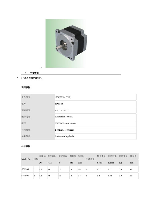
主要特点
57系列两相步进电机
通用规格
步距精度
+5%(整步、空载)
温升
80°CMax
环境温度
-10°C -- +50°C
绝缘电阻
100MΩmin.500VDC
1N4000系列普通二极管型号大全

MA5091
9.1
5
500
BZX55C51
51
2.5
500
MA5100
10
5
500
BZX55C56
56
2.5
500
MA5110
11
5
500
BZX55C62
62
2.5
500
MA5120
12
5
500
BZX85C2V7
2.7
80
1300
MA5130
13
5
500
BZX85C3V0
3.0
80
1300
MA5150
MA3056
5.6
5
150
MA1082
8.2
5
400
MA3062
6.2
5
150
MA1091
9.1
5
400
MA3082
8.2
5
150
MA1100
10
5
400
MA3091
9.1
5
150
MA1110
11
5
400
MA3100
10
5
150
MA1114
11.4
10
400
MA3110
11
5
150
MA1120
12
5
5.6
5.0
45
10
DO-41
稳压二极管
008
1N4735
6.2
2.0
41
10
DO-41
稳压二极管
009
1N4736
6.8
峰值力仪表说明书
8604型峰值测试仪使用说明书●使用前请仔细阅读本产品说明书●请妥善保管本产品说明书,以备查阅深圳市鸿伟成计量控制有限公司目录1.0 概述 (1)1.1主要特点 (1)1.2技术指标 (1)1.2.1 负载能力 (1)1.2.2 性能 (1)1.2.3 电源 (1)1.2.4 温度和湿度 (1)1.2.5 外形尺寸(尺寸单位为毫米) (2)2.0安装 (2)2.1仪表固定 (2)2.2峰值力测试仪电气连接 (3)2.2.1 峰值力测试仪后视图 (3)2.2.2 电源连接 (3)2.2.3 传感器与峰值力测试仪连接 (3)2.2.4 串行口通讯线连接 (3)2.2.5 继电器控制输出 (3)3.0 操作说明 (4)3.1显示面板 (4)3.2基本操作 (4)3.3仪表上电 (5)4.0 设定 (5)4.1标定 (5)4.1.1 参数确定 (5)4.1.2 标定步骤 (5)4.2设置上下限(继电器输出) (6)4.2.1 设置步骤 (6)4.2.2 选择继电器的输出模式 (6)4.3设置日期与时间 (8)5.0 打印机 (9)5.1打印格式 (9)5.2改变字体大小 (9)6.0 标定头 (9)7.0 使用注意事项 (9)V er1.2/05/12/141.0 概述8604型峰值力测试仪的信号采集使用高速、高精度的24位专用A/D转换器, 使用高速单片机对信号进行运算处理,及时捕捉瞬间的最大值。
小巧的盘装式铝合金外壳,可方便的嵌入各种控制柜。
是各种力值试验机理想的配套仪表。
1.1 主要特点∙高精度、高分辨率∑-△型A/D转换,最大A/D脉冲数:1,000,000 ∙数据采样速率:120次/秒,显示刷新:10次/秒∙两点(常开)继电器输出,动作模式可设定(上下限报警)∙数字通讯接口,RS232C方式(选配)∙具有实时时钟,切换显示时间与日期∙20位LED数码管显示,可以同时显示时间(8位)、当前值(6位)与峰值(6位)∙显示单位kg与N可以转换∙具有打印接口,可以选配微型打印机1.2 技术指标1.2.1 负载能力激励电压:5.0VDC,可驱动8只350Ω的模拟式传感器。
常用国产电子管参数

—
—
—
—
—
5、5
4、5
1700
100
—
—
负载2、2kΩ
6Z4
6、3
0、6
2×350
72
—
—
—
—
—
—
7
5、7
1000
2 5
—
—
负载5、2kΩ
6Z5P
6、3
0、6
2×400
70
—
—
—
—
—
—
6、9
5、7
1100
3 0
—
—
负载5、7kΩ
6HZ
6、3
0、3
2×150
17
—
—
—
—
—
—
7
5、7
450
3
—
—
负载10kΩ
12、5
27
6、9
5、7
130
2
—
—
Rg<1MΩ
6N12P
6、3
0、9
180
23
-7
—
—
2、4
7
17
6、9
5、7
300
4、2
—
—
Rg<100kΩ
6N13P
6、3
2、5
90
80±32
-30
—
—
Ri≤460Ω
5
—
6、9
5、7
300
13
—
—
Rg<1MΩ
6N15
6、3
0、45
100
90
Rk=90Ω
—
XL6004芯片资料
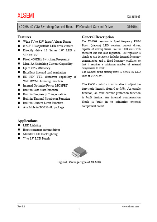
400KHz 42V 3A Switching Current Boost LED Constant Current Driver XL6004FeaturesWide 5V to 32V Input Voltage Range 0.22V FB adjustable LED drive current Directly drive 12 Series 1W LED atVIN>=10VFixed 400KHz Switching Frequency Max. 3A Switching Current Capability Up to 92% efficiencyExcellent line and load regulationEN PIN TTL shutdown capability &With PWM Dimming Function Internal Optimize Power MOSFET Built in Soft-Start FunctionBuilt in Frequency Compensation Built in Thermal Shutdown Function Built in Current Limit Function Available in TO252-5L packageApplicationsLED LightingBoost constant current driver Monitor LED Backlighting 7’ to 15’ LCD PanelsGeneral DescriptionThe XL6004 regulator is fixed frequency PWM Boost (step-up) LED constant current driver, capable of driving Series 1W/3W LED units with excellent line and load regulation. The regulator is simple to use because it includes internal frequency compensation and a fixed-frequency oscillator so that it requires a minimum number of external components to work.The XL6004 could directly drive 12 Series 1W LED units at VIN>12V.The PWM control circuit is able to adjust the duty ratio linearly from 0 to 95%. An enable function, an over current protection function is built inside. An internal compensation block is built in to minimize external component count.Figure1. Package Type of XL6004400KHz 42V 3A Switching Current Boost LED Constant Current Driver XL6004400KHz 42V 3A Switching Current Boost LED Constant Current Driver XL6004Figure4. XL6004 Typical Application Circuit400KHz 42V 3A Switching Current Boost LED Constant Current Driver XL6004400KHz 42V 3A Switching Current Boost LED Constant Current Driver XL6004400KHz 42V 3A Switching Current Boost LED Constant Current Driver XL6004400KHz 42V 3A Switching Current Boost LED Constant Current Driver XL6004Figure6. XL6004 System Parameters Test Circuit (10V ~ 12 x 1W LED) Typical System Application for VIN>=12V to driver 6 x 3W series LED units400KHz 42V 3A Switching Current Boost LED Constant Current Driver XL6004 Figure8. XL6004 System Parameters Test Circuit (12V ~ 12 x 24 White LED)400KHz 42V 3A Switching Current Boost LED Constant Current Driver XL6004Package InformationTO252-5L。
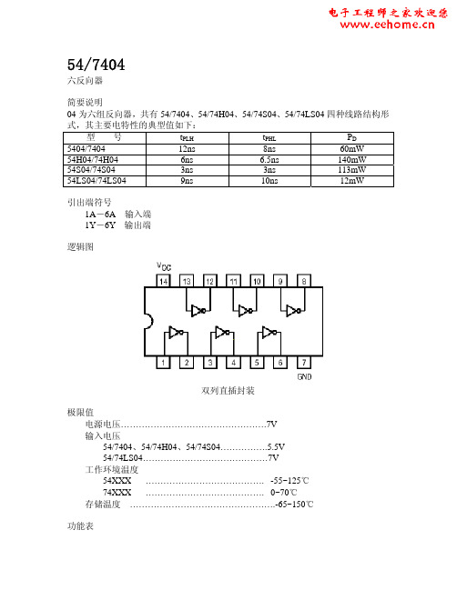
7404中文资料
-20 -55 -18 -55
ICCH输出高电平时电源电流
Vcc=最大
12
ICCL输出低电平时电源电流
Vcc=最大
33
‘H04 最小 最大
-1.5
2.4 2.4
0.4 0.4 1
50
-2
-40 -100 -40 -100
26 58
‘S04 最小 最大
-1.2 2.5 2.7
0.5 0.5 1
3ns
3ns
113mW
54LS04/74LS04
9ns
10ns
12mW
引出端符号 1A-6A 输入端 1Y-6Y 输出端
逻辑图
双列直插封装
极限值 电源电压………………………………………….7V 输入电压 54/7404、54/74H04、54/74S04…………….5.5V 54/74LS04……………………………………7V 工作环境温度 54XXX …………………………………. -55~125℃ 74XXX …………………………………. 0~70℃ 存储温度 ………………………………………….-65~150℃
参数
tPLH输出由低到高传输延迟时间 tPHL输出由高到低传输延迟时间
测试条件
Vcc =5V,CL=50Pf(‘H04 为 25Pf) RL=400Ω(‘H04最大 22
15
‘H04 最大
10
10
‘S04 最大 4.5
5
‘LS04 最大 15
5.5 4.5 5.25 4.75
5 5
5.5 5.25
V
输入高电平电压ViH
2
输入低电平 54
电ViL
74
输出高电平电流IOH
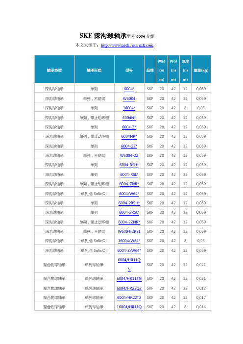
SKF深沟球轴承6004
聚合物球轴承 聚合物球轴承 聚合物球轴承 聚合物球轴承
轴承形式
单列 单列,不锈钢
单列 单列,带止动环槽
单列 单列,带止动环槽
单列 单列,不锈钢
单列 单列 单列,带止动环槽 单列,含 SolidOil 单列 单列 单列,带止动环槽 单列,不锈钢 单列,含 SolidOil 单列,含 SolidOil
6004-Z*
SKF 20 42 12 0,069
6004NR*
SKF 20 42 12 0,069
6004-2Z*
SKF 20 42 12
0,069
W6004-2Z SKF 20 42 12 0,069
6004-RSH* SKF 20 42 12 0,069
6004-RSL* SKF 20 42 12 0,069
9/HC5C3WT
0,014 0,011 0,011 0,069 0,068 0,069 0,062
6004-ZNR* SKF 20 42 12 0,069
6004/W64* SKF 20 42 12 0,069
6004-2RSH* SKF 20 42 12 0,069
6004-2RSL* SKF 20 42 12 0,069
6004-2ZNR* SKF 20 42 12 0,069
W6004-2RS1 SKF 20 42 12 0,069
SKF 深沟球轴承型号 6004 介绍
本文来源于:
轴承类型
深沟球轴承 深沟球轴承 深沟球轴承 深沟球轴承 深沟球轴承 深沟球轴承 深沟球轴承 深沟球轴承 深沟球轴承 深沟球轴承 深沟球轴承 深沟球轴承 深沟球轴承 深沟球轴承 深沟球轴承 深沟球轴承 深沟球轴承 深沟球轴承
ZXMS6004FFTA;中文规格书,Datasheet资料

60V N-channel self protected enhancement mode Intellifet MOSFETSummaryContinuous drain source voltage 60 V On-state resistance500 m ΩNominal load current (V IN = 5V) 1.3 A Clamping energy90mJDescriptionThe ZXMS6004FF is a self protected low side MOSFET with logic level input. It integrates over-temperature, over-current, over-voltage (active clamp) and ESD protected logic level functionality. The ZXMS6004FF is ideal as a general purpose switch driven from 3.3V or 5V microcontrollers in harsh environments where standard MOSFETs are not rugged enough.Features•Compact high power dissipation package •Low input current•Logic Level Input (3.3V and 5V)•Short circuit protection with auto restart •Over voltage protection (active clamp)•Thermal shutdown with auto restart •Over-current protection •Input Protection (ESD)•High continuous current ratingOrdering informationDevice Part markReel size(inches)Tape width (mm)Quantity per reelZXMS66004FFTA 1K6712 embossed3,000 unitsApplication information•Especially suited for loads with a high in-rush current such as lamps and motors.•All types of resistive, inductive and capacitive loads in switching applications.•μC compatible power switch for 12V and 24V DC applications.•Automotive rated.•Replaces electromechanical relays and discrete circuits.•Linear Mode capability - the current-limiting protection circuitry is designed to de-activate at low V DS to minimise on state power dissipation. The maximum DC operating current is therefore determined by the thermal capability of the package/board combination, rather than by the protection circuitry. This does not compromise the product’s ability to self-protect at low V DS.Absolute maximum ratingsThermal resistanceNOTES(a)For a device surface mounted on a 15mm x 15mm single sided 1oz weight copper on 1.6mm FR4 board, in still air conditions.(b)F or a device surface mounted on 50mm x 50mm single sided 2oz weight copper on 1.6mm FR4 board in still air conditions.(c)Thermal resistance from junction to the mounting surface of the drain pin.ParameterSymbol Limit Unit Continuous Drain-Source voltageV DS 60V Drain-Source voltage for short circuit protection V DS(SC)36V Continuous input voltage V IN -0.5 ... +6V Continuous input current -0.2V ≤V IN ≤6VV IN <-0.2V or V IN >6VI INNo limit │I IN │≤2mAOperating temperature range T j ,-40 to +150°C Storage temperature range T stg -55 to +150°C Power dissipation at T A =25°C (a)Linear derating factorP D 0.836.66W mW/°C Power dissipation at T A =25°C (b) Linear derating factorP D 1.512.0W mW/°C Pulsed drain current @ V IN =3.3V I DM 2A Pulsed drain current @ V IN =5VI DM 2.5A Continuous source current (Body Diode) (a)I S 1A Pulsed dource current (Body Diode) I SM 5A Unclamped single pulse inductive energy, Tj=25°C, I D =0.5A, V DD =24VE AS 90mJ Electrostatic discharge (Human body model)V ESD 4000V Charged device modelV CDM 1000VParameterSymbo Value Unit Junction to ambient (a)R θJA 150°C/W Junction to ambient (b)R θJA 83°C/W Junction to case (c)R θJC44°C/WRecommended operating conditionsThe ZXMS6004FF is optimised for use with µC operating from 3.3V and 5V supplies.CharacteristicsSymbolDescriptionMinMaxUnitsV IN Input voltage range0 5.5V T A Ambient temperature range-40125°C V IH High level input voltage for MOSFET to be on 3 5.5V V IL Low level input voltage for MOSFET to be off00.7V V PPeripheral supply voltage (voltage to which load is referred)36VElectrical characteristics (at T amb = 25°C unless otherwise stated).Notes:(d)The drain current is restricted only when the device is in saturation (see graph ‘typical output characteristic’). This allows the device to be used in the fully on state without interference from the current limit. The device is fully protected at all drain currents, as the low power dissipation generated outside saturation makes current limit unnecessary.ParameterSymbol Min Typ Max Unit ConditionsStatic Characteristics Drain-Source clamp voltage V DS(AZ)606570V I D =10mA Off-state drain Ccrrent I DSS 500nA V DS =12V, V IN =0V Off-state drain current I DSS 1μA V DS =36V, V IN =0V Input threshold voltage V IN(th)0.71 1.5V V DS =V GS , I D =1mA Input current I IN 60100μA V IN =+3V Input currentI IN120200μA V IN =+5V Input current while over temperature active220μA V IN =+5VStatic Drain-Source on-state resistanceR DS(on)400600m ΩV IN =+3V, I D =0.5A Static Drain-Source on-state resistanceR DS(on)350500m ΩV IN =+5V, I D =0.5A Continuous drain current (a) I D 0.9A V IN =3V; T A =25°C Continuous drain cCurrent(a)I D 1.0A V IN =5V; T A =25°C Continuous drain current (b)I D 1.2A V IN =3V; T A =25°C Continuous drain current (b)I D 1.3AV IN =5V; T A =25°C Current limit I D(LIM)0.7 1.7A V IN =+3V,Current limit (c)I D(LIM)12.2A V IN =+5VDynamic characteristics Turn-on delay time t d(on)5μs V DD =12V, I D =0.5A, V GS =5VRise timet r 10μs Turn-off delay time t d(off)45μs Fall time f f15μsElectrical characteristics - continuedNote:(a)Over-temperature protection is designed to prevent device destruction under fault conditions. Fault conditions are considered as “outside” normal operating range, so this part is not designed to withstand over-temperature for extended periods..ParameterSymbolMinTypMaxUnitConditionsOver-temperature protection Thermal overload trip temperature (a)TJT150175°C Thermal hysteresis (a)10°CTypical characteristicsPackage information - SOT23FNote: Controlling dimensions are in millimeters. Approximate dimensions are provided in incheslimeters Inches limeters Inches Min.Max.Min.Max.Min.Max.Min.Max.A 0.80 1.000.03150.0394E 2.30 2.500.09060.0984A10.000.100.000.0043E1 1.50 1.700.05900.0669b 0.350.450.01530.0161L 0.480.680.01890.0268c 0.100.200.00430.0079L10.300.500.01530.0161D 2.803.000.11020.1181R 0.050.150.00190.0059e 0.95 ref 0.0374 ref O 0°12°0°12°e11.802.000.07090.0787-----Sales officesThe Americas3050 E. Hillcrest Drive Westlake Village,CA 91362-3154Tel: (+1) 805 446 4800 Fax: (+1) 805 446 4850EuropeKustermann-ParkBalanstraße 59,D-81541 MünchenGermanyTel: (+49) 894 549 490Fax: (+49) 894 549 4949Taiwan7F, No. 50,Min Chuan RoadHsin-TienTaipei, TaiwanTel: (+886) 289 146 000Fax: (+886) 289 146 639ShanghaiRm. 606, No.1158Changning RoadShanghai, ChinaTel: (+86) 215 241 4882Fax (+86) 215 241 4891ShenzhenANLIAN Plaza, #4018Jintian RoadFutian CBD,Shenzhen, ChinaTel: (+86) 755 882 849 88Fax: (+86) 755 882 849 99Korea6 Floor, Changhwa B/D,1005-5 Yeongtong-dong,Yeongtong-gu, Suwon-si,Gyeonggi-do, Korea 443-813Tel: (+82) 312 731 884Fax: (+82) 312 731 885DefinitionsProduct changeDiodes Incorporated reserves the right to alter, without notice, specifications, design, price or conditions of supply of any product or service. Customers are solely responsible for obtaining the latest relevant information before placing orders.Applications disclaimerThe circuits in this design/application note are offered as design ideas. It is the responsibility of the user to ensure that the circuit is fit for the user’s application and meets with the user’s requirements. No representation or warranty is given and no liability whatsoever is assumed by Diodes Inc. with respect to the accuracy or use of such information, or infringement of patents or other intellectual property rights arising from such use or otherwise. Diodes Inc. does not assume any legal responsibility or will not be held legally liable (whether in contract, tort (including negligence), breach of statutory duty, restriction or otherwise) for any damages, loss of profit, business, contract, opportunity or consequential loss in the use of these circuit applications, under any circumstances.Life supportDiodes Zetex products are specifically not authorized for use as critical components in life support devices or systems without the express written approval of the Chief Executive Officer of Diodes Incorporated. As used herein:A. Life support devices or systems are devices or systems which:1.are intended to implant into the bodyor2.support or sustain life and whose failure to perform when properly used in accordance with instructions for use provided in thelabeling can be reasonably expected to result in significant injury to the user.B. A critical component is any component in a life support device or system whose failure to perform can be reasonably expected tocause the failure of the life support device or to affect its safety or effectiveness.ReproductionThe product specifications contained in this publication are issued to provide outline information only which (unless agreed by the company in writing) may not be used, applied or reproduced for any purpose or form part of any order or contract or be regarded as a representation relating to the products or services concerned.Terms and ConditionsAll products are sold subjects to Diodes Inc. terms and conditions of sale, and this disclaimer (save in the event of a conflict between the two when the terms of the contract shall prevail) according to region, supplied at the time of order acknowledgement.For the latest information on technology, delivery terms and conditions and prices, please contact your nearest Diodes Zetex sales office.Quality of productDiodes Zetex Semconductors Limited is an ISO 9001 and TS16949 certified semiconductor manufacturer.To ensure quality of service and products we strongly advise the purchase of parts directly from Diodes Inc. or one of our regionally authorized distributors. For a complete listing of authorized distributors please visit: or Diodes Inc. does not warrant or accept any liability whatsoever in respect of any parts purchased through unauthorized sales channels.ESD(Electrostatic discharge)Semiconductor devices are susceptible to damage by ESD. Suitable precautions should be taken when handling and transporting devices. The possible damage to devices depends on the circumstances of the handling and transporting, and the nature of the device. The extent of damage can vary from immediate functional or parametric malfunction to degradation of function or performance in use over time. Devices suspected of being affected should be replaced.Green complianceDiodes Inc. is committed to environmental excellence in all aspects of its operations which includes meeting or exceeding regulatory requirements with respect to the use of hazardous substances. Numerous successful programs have been implemented to reduce the use of hazardous substances and/or emissions.All Diodes Zetex components are compliant with the RoHS directive, and through this it is supporting its customers in their compliance with WEEE and ELV directives.Product status key:“Preview”Future device intended for production at some point. Samples may be available“Active”Product status recommended for new designs“Last time buy (LTB)”Device will be discontinued and last time buy period and delivery is in effect“Not recommended for new designs”Device is still in production to support existing designs and production“Obsolete”Production has been discontinuedDatasheet status key:“Draft version”This term denotes a very early datasheet version and contains highly provisional information, whichmay change in any manner without notice.“Provisional version”This term denotes a pre-release datasheet. It provides a clear indication of anticipated performance.However, changes to the test conditions and specifications may occur, at any time and without notice.“Issue”This term denotes an issued datasheet containing finalized specifications. However, changes tospecifications may occur, at any time and without notice.分销商库存信息: DIODESZXMS6004FFTA。
- 1、下载文档前请自行甄别文档内容的完整性,平台不提供额外的编辑、内容补充、找答案等附加服务。
- 2、"仅部分预览"的文档,不可在线预览部分如存在完整性等问题,可反馈申请退款(可完整预览的文档不适用该条件!)。
- 3、如文档侵犯您的权益,请联系客服反馈,我们会尽快为您处理(人工客服工作时间:9:00-18:30)。
V RRM= 6000 V I F(AV)M= 1100 A I FSM= 18×103A V(T0)= 1.5 V r T= 0.6 mΩV DC-link= 3800 V Fast Recovery Diode5SDF 10H6004Doc. No. 5SYA1109-02 Oct. 06•Patented free-floating silicon technology•Low on-state and switching losses•Optimized for use as freewheeling diode in high-voltage GTO converters•Industry standard housing•Cosmic radiation withstand ratingBlockingMaximum rated values 1)Parameter Symbol Conditions Value Unit Repetitive peak reverse voltage V RRM f = 50 Hz, t p = 10ms, T vj = 125°C 6000 VPermanent DC voltage for 100 FIT failure rate V DC-link Ambient cosmic radiation at sea level in openair. (100% Duty)3800 VCharacteristic valuesParameter Symbol Conditions min typ max Unit Repetitive peak reverse current I RRM V R = V RRM, T vj = 125°C 50 mA Mechanical dataMaximum rated values 1)Parameter Symbol Conditions min typ max Unit Mounting force F m 36 40 44 kN Acceleration a Device unclamped 50 m/s2 Acceleration a Device clamped 200 m/s2 Characteristic valuesParameter Symbol Conditions min typ max Unit Weight m0.83 kg Housing thickness H26.2 26.6 mm Surface creepage distance D S 30 mm Air strike distance D a 20 mm Note 1 Maximum rated values indicate limits beyond which damage to the device may occur元器件交易网ABB Switzerland Ltd, Semiconductors reserves the right to change specifications without notice.On-stateMaximum rated values 1)ParameterSymbol Conditions mintyp max Unit Max. average on-state currentI F(AV)MHalf sine wave, T C = 85 °C 1100 A Max. RMS on-state current I F(RMS)1700A Max. peak non-repetitive surge current I FSM18×103A Limiting load integral I 2t t p = 10 ms, T vj = 125°C, V R = 0 V1.62×106 A 2s Max. peak non-repetitive surge current I FSM44×103A Limiting load integralI 2tt p = 1 ms, T vj = 125°C, V R = 0 V968×103A 2s Characteristic valuesParameter Symbol Conditions min typ max Unit On-state voltage V F I F = 2500 A, T vj = 125°C 3 V Threshold voltage V (T0) 1.5 V Slope resistancer TT vj = 125°CI F = 200...6000 A0.6m ΩTurn-onCharacteristic valuesParameterSymbol Conditions mintypmax Unit Peak forward recovery voltageV FRMdI F /dt = 500 A/µs, T vj = 125°C150VTurn-offCharacteristic valuesParameterSymbol Conditions mintypmax Unit Reverse recovery current I RM 1000 A Reverse recovery charge Q rr 6000 µC Turn-off energy E rrdi/dt = 300 A/µs, I FQ = 1000 A, T j = 125°C, V RM = 2900 V, C S = 3 µF (GTO snubber circuit)5JThermalMaximum rated values 1)Parameter Symbol Conditions min typ max Unit Operating junction temperature rangeT vj-40 125 °C Storage temperature range T stg-40 125 °C Characteristic valuesParameterSymbol Conditionsmin typ max Unit Thermal resistance junction to case R th(j-c) Double-side cooled F m = 36...44 kN 12 K/kW R th(j-c)A Anode-side cooled F m = 36...44 kN 24 K/kWR th(j-c)CCathode-side cooled F m = 36...44 kN 24K/kW Thermal resistance case to heatsink R th(c-h) Double-side cooled F m = 36...44 kN 3 K/kWR th(c-h)Single-side cooled F m = 36...44 kN6K/kWAnalytical function for transient thermalimpedance:)e -(1R = (t)Z n1i t/-i th c)-th(j ∑=i τ i 1 2 3 4 R th i (K/kW)7.440 2.000 1.840 0.710τi (s)0.47000.09100.01000.0047Fig. 1 Transient thermal impedance junction-to-caseFig. 2 Max. on-state voltage characteristicsFig. 3 Surge on-state current vs. pulse length. Half-sine waveFig. 4 Forward recovery vs. turn on di/dt (max.values)Fig. 5General current and voltage waveformsFig. 6Test circuit.ABB Switzerland Ltd, Semiconductors reserves the right to change specifications without notice.ABB Switzerland Ltd Doc. No. 5SYA1109-02 Oct. 06Semiconductors Fabrikstrasse 3CH-5600 Lenzburg, SwitzerlandTelephone +41 (0)58 586 1419 Fax +41 (0)58 586 1306Fig. 7 Outline drawing, all dimensions are in millimeters and represent nominal values unless stated otherwiseRelated documents:Doc. Nr Titel5SYA 2036 Recommendations regarding mechanical clamping of Press Pack High Power Semiconductors5SZK 9104 Specification of environmental class for pressure contact diodes, PCTs and GTO, STORAGE available on request, please contact factory5SZK 9105Specification of environmental class for pressure contact diodes, PCTs and GTO, TRANSPORTATION available on request, please contact factoryPlease refer to /semiconductors for current version of documents.。