HBI241N wk 1 lec s2 13 6up[1]
BTS4141N中文资料
Value
Unit
-0,31)...48
V
-10...Vbb
self limited
A
±5
mA
-0.5
A
internal limited °C
-55 ... +150
1.4
W
0.7
J
V
83 kV
±1 ±5
1defined by Ptot 2At VIN > Vbb, the input current is not allowed to exceed ±5 mA. 3defined by Ptot 4Device on 50mm*50mm*1.5mm epoxy PCB FR4 with 6 cm2 (one layer, 70µm thick) copper area for Vbb connection. PCB is vertical without blown air. 5not subject to production test, specified by design 6VLoaddump is setup without the DUT connected to the generator per ISO 7637-1 and DIN 40839 . Supply voltages higher than Vbb(AZ) require an external current limit for the GND pin, e.g. with a 150Ω resistor in GND connection. A resistor for the protection of the input is integrated.
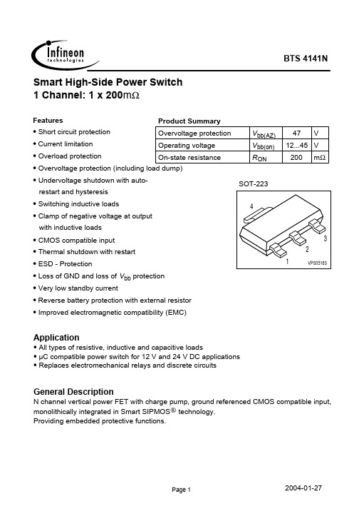
General Description
Waters 2414示差检测器中文说明书

WatersHPLC SystemBasic Teaching Material For 2414 Refractive Index Detector 沃特斯高效能液相層析系統-2414折射率偵測器基礎操作指引文案大全Content一、儀器介紹與功能說明 (3)1. 儀器外觀 (3)2. 螢幕說明 (3)二、開機方法 (4)三、操作畫面說明 (4)四、溫度設定 (6)五、IEEE 位址 ( IEEE Address ) 設定 (7)六、液晶螢幕明暗度設定 (8)七、關機方法: (8)一、 儀器介紹與功能說明1. 儀器外觀2. 螢幕說明a. RIU Modeb. 410 Mode液晶顯示幕操作面板二、開機方法a.將2414 RI Detector的電源開關打開至ON(1)的位置,機器開始作自我檢查。
b.待儀器自我測試完畢後,即出現以下畫面,此乃表示開機測試正常。
三、操作畫面說明液晶顯示幕四、溫度設定a.按溫度設定鍵。
液晶顯示幕b.進入溫度設定畫面。
c.按<▲>/<▼>至Detector(Det)或Column(Col) 溫度設定位置(Set)。
d.輸入預設定之溫度大小。
e.按<HOME>鍵回復至初始畫面。
五、IEEE 位址 ( IEEE ADDRESS ) 設定a.按<HOME>鍵回復至初始畫面。
液晶顯示b.按<Shift>及<CONFIGURE>鍵,至系統設定功能。
c.將游標移動至IEEE位址設定位置,輸入適當之位址編號。
( 位址編號不能與其他儀器/設備相同 )d.設定完畢後,按<HOME>鍵回復至初始畫面。
六、液晶螢幕明暗度設定a.按<HOME>鍵回復至初始畫面。
液晶顯示b.按<Shift>及<Contrast>鍵,至螢幕明按度設定功能。
c.按<▲>/<▼>調整螢幕適合之明暗度。
HNIO-241R中文资料

DEVELOPER KIT (Info: click here)General SpecificationsRF Frequency 902 -927 MHzSpreading Method FCC Part 15.247, license free Modulation GFSKTransmit Power 500mW, 100mW, 10mW, software selectable; 1W, 200mW, 20mW with integral patch antenna modulesReceive Sensitivity -103 dBm for 10-5 BER / -108dBm with integral patch antenna module RF Channels 54RF Data Rate 172.8 KbpsI/O4 – Opto-Isolated Inputs 0-30V4 – SPST (Form A) Relays (NO/COM) 250VAC, 5A 1 – SPST Relay (NO;COM) RF Link 1 – RS-232 D9 Serial Port Operating Voltage +9Vdc – +30Vdc Operating Temperature-40°C to +70°CProviding multi-point, bidirectional communications, 4 Form A relay outputs, and Class I Div 2 certification, the HN 2.4GHz spread spectrum wireless relay I/O modems are the ideal solution for industrial andcommercial monitoring and control applications. All HNIO modems include RFM frequency hopping spread spectrum radio technology that has been field-proven to provide reliable, robust wireless communications in harsh RF environments.900MHz Relay I/O Wireless ModemHNIO-241R HNIO-241RR HNIO-241RX Features:•Full multi-point, bidirectional operation •4 channels•Fully configurable through DIP switches •Frequency hopping spread spectrum •Class I Div 2 certified •2.4GHz•Operates over an input voltage range of +9Vdc to +30Vdc making it suitable for battery and solar power sourcesBenefits:•Ability to confirm remote status •Operate multiple devices from one modem•Reliable performance in high RF noise environments•Deploy in a wide variety of locations •Useful for industrial and outdoor applications with a -40°C to +70°C operating temperature range and certified for hazardous location use900MHz Relay I/O Wireless ModemMechanical SpecificationsModel HNIO-241R HNIO-241RR HNIO-241RXEnclosure Material ABS ABS(network interface unit)Polycarbonate NEMA 4X(remote radio unit)ABS(network interface unit)Polycarbonate NEMA 4X(remote radio unit)Enclosure Size 138 x 108 x 47201 x 144 x 53(network interface unit)130 x 79 x 35(remote radio unit)201 x 144 x 53(network interface unit)130 x 79 x 35(remote radio unit)Antenna Type2dBi included3dBi integral patch2dBi included Antenna Type Reverse TNC n/a Reverse TNCConnector1 PinoutPin 1 - RFLink NOPin 2 - RFLink COMPin 3 - Input1 +Pin 4 - Input1 -Pin 5 - Input2 +Pin 6 - Input2 -Pin 7 - Input3 +Pin 8 - Input3 -Pin 9 - Input4 +Pin 10 - Input4 -Pin 11 - IN APin 12 - IN BPin 13 - OUT APin 14 - OUT BPin 15 - GNDPin 16 - GNDConnector2 PinoutPin 1 - Relay1 NOPin 2 - Relay1 COMPin 3 - Relay2 NOPin 4 - Relay2 COMPin 5 - Relay3 NOPin 6 - Relay3 COMPin 7 - Relay4 NOPin 8 - Relay4 COMFlexible I/OFour 250VAC, 5 Ampere Form A relay contacts are controlled by 4 opto-isolated inputs on the companion radio. Offering full bidirectional operation, the four inputs on one end control the relays of the second modem while the inputs of the second radio control the relays of the first modem – simultaneously. The HNIO-R uses sealed relays allowing Class I Div 2 certification. Each base radio can connect up to four remote radios. Four base radios can be located together.Fully ConfigurableThe HNIO-241R is fully configurable through DIP switches or an intuitive terminal interface. Configurable options include edge or level triggered inputs, positive or negative activation signals (selectable per channel), frequency of transmission from continuous to once every 45 minutes, and an RF link interruption fail-safe mode. A NO relay contact indicates RF link status.Industrial NetworkingThe HNIO-241R is designed for industrial and outdoor applications with a -40°C to +70°C operating temperature range. The HNIO-241R can operate over an input voltage range of +9Vdc to +30Vdc making it suitable for battery and solar power sources. The HNIO-241R is Class I Div 2 certified for hazardous location use. The standard DIN-rail enclosure or optional six inch cabinet allows easy installation whatever the application. The HNIO-241RR andHNIO-241RX are external versions where the remote radio is housed in a separate NEMA 4X rated enclosure with either an integral patch antenna or a reverse TNC antenna connector.FHSS TechnologyThe frequency hopping spread spectrum technology used in the HNIO-241R has been powering a wide variety of mission-critical industrial applications for years and embodies extensive experience in spread spectrum radio design. With superior immunity to jamming and multipath fade, RFM FHSS technology transmits data over the air at a crisp 460.8Kbps rate providing short latencies and plenty of bandwidth. Operating in the 2.4GHz band, the HNIO-241R can be deployed license-free worldwide.。
HPDL-2416中文资料

3-175Four Character Smart Alphanumeric Displays Technical DataFeatures• Smart Alphanumeric Display Built-in RAM, ASCII Decoder and LED Drive Circuitry• Wide Operating Temperature Range-40°C to +85°C • Fast Access Time 160 ns• Excellent ESD Protection Built-in Input Protection Diodes • CMOS IC for Low Power Consumption• Full TTL Compatibility Over Operating Temperature Range V IL = 0.8 V V IH = 2.0 V• Wave Solderable • Rugged Package Construction • End-Stackable• Wide Viewing AngleTypical Applications• Portable Data Entry Devices • Medical Equipment• Process Control Equipment • Test Equipment• Industrial Instrumentation • Computer Peripherals • Telecommunication InstrumentationDescriptionThe HPDL-1414 and 2416 are smart, four character, sixteen-segment, red GaAsP displays. The HPDL-1414 has a characterheight of 2.85 mm (0.112"). The HPDL-2416 has a characterheight of 4.10 mm (0.160"). The on-board CMOS IC contains memory, ASCII decoder, multi-plexing circuitry and drivers. The monolithic LED characters are magnified by an immersion lens which increases both character size and luminous intensity. The encapsulated dual-in-line package provides a rugged, environment-ally sealed unit.HPDL-1414HPDL-2416ESD WARNING: STANDARD CMOS HANDLING PRECAUTIONS SHOULD BE OBSERVED WITH THE HPDL-1414 AND HPDL-2416.The HPDL-1414 and 2416incorporate many improvements over competitive products. They have a wide operating tempera-ture range, very fast IC access time, and improved ESD protec-tion. The displays are also fully TTL compatible, wave solderable,and highly reliable. These displays are ideally suited for industrial and commercial applications where a good-looking, easy-to-use alphanumeric display is required.H5964-6381E3-176Absolute Maximum RatingsSupply Voltage, V DD to Ground......................................-0.5 V to 7.0 V Input Voltage, Any Pin to Ground........................-0.5 V to V DD + 0.5 V Free Air Operating Temperature Range, T A [1]...............-40°C to +85°C Relative Humidity (non-condensing) at 65°C .................................90%Storage Temperature, T S .............................................. -40°C to +85°C Maximum Solder Temperature, 1.59 mm (0.063 in.)below Seating Plane, t < 5 sec.................................................260°C ESD Protection @ 1.5 k Ω, 100 pF...................... V Z = 2 kV (each Pin)*All typicals at T A = 25°C.Package DimensionsHPDL-14143-177HPDL-2416Recommended Operating ConditionsParameterSym.Min.Nom.Max.Units Supply VoltageV DD4.55.05.5VDC Electrical Characteristics over Operating Temperature RangeNotes:1. V DD = 5.5 V.2. “%” illuminated in all four characters.3. Measured at five seconds.4. Cursor character is sixteen segments and DP ON.5. Power Dissipation = (V DD)(I DD) for 10 segments ON.Optical Characteristics at 25°C[6]3-1783-179AC Timing Characteristics over Operating Temperature Range at V CC= 4.5 VParameter Symbol -20°C t MIN25°C t MIN70°C t MINUnits Address Setup Time t AS 90115150ns Write Delay Time t WD 101520ns Write Timet W 80100130ns Data Setup Time t DS 406080ns Data Hold Time t DH 404550ns Address Hold Timet AH 404550ns Chip Enable Hold Time [1]t CEH 404550ns Chip Enable Setup Time [1]t CES 90115150ns Clear Time [1]t CLR2.43.54.0ms Access Time 130160200ns Refresh Rate420-790310-630270-550HzNote:1. HPDL-2416 only.Timing Diagram3-180Character SetMagnified Character Font DescriptionHPDL-1414HPDL-2416Relative Luminous Intensity vs. Temperature3-181Electrical DescriptionDisplay Internal Block Diagram HPDL-1414Figure 1 shows the internal block diagram of the HPDL-1414. It consists of two parts: the display LEDs and the CMOS IC. The CMOS IC consists of a four-word ASCII memory, a 64-word charac-ter generator, 17 segment drivers,four digit drivers, and thescanning circuitry necessary to multiplex the four monolithic LED characters. In normaloperation, the divide-by-four counter sequentially accesses each of the four RAM locations and simultaneously enables the appropriate display digit driver.The output of the RAM is decoded by the character generator which,in turn, enables the appropriate display segment drivers. Seven-bit ASCII data is stored in RAM.Since the display uses a 64-character decoder, half of the possible 128 input combinations are invalid. For each display location where D 5 = D 6 in theASCII RAM, the display character is blanked.Data Entry HPDL-1414Figure 2 shows a truth table for the HPDL-1414. Data is loaded into the display through theDATA inputs (D 6-D 0), ADDRESS inputs (A 1-A 0), and WRITE (WR).After a character has been written to memory, the ICdecodes the ASCII data, drives the display and refreshes itwithout any external hardware or software.Figure 1. HPDL-1414 Internal Block Diagram.3-182If the clear input (CLR) equals zero for one internal display cycle (4 ms minimum), the data in the ASCII RAM will be rewritten with zeroes and the display will be blanked. Note that the blanking input (BL) must be equal to logical one during this time.Data Entry HPDL-2416Figure 4 shows a truth table for the HPDL-2416 display. Setting the chip enables (CE 1, CE 2) to their low state and the cursor select (CU) to its high state will enable data loading. The desired data inputs (D 6-D 0) and address inputs (A 1, A 0) as well as the chip enables (CE 1, CE 2) and cursor select (CU) must be held stable during the write cycle to ensure that the correct data is stored into the display. Valid ASCII data codes are shown in Figure 1. The display accepts standard seven-bit ASCII data. Note that D 6 ≠ D 5for the codes shown in Figure 4.If D 6 = D 5 during the write cycle,then a blank will be stored in the display. Data can be loaded into the display in any order. Note that when A 1 = A 0 = 0, data is stored in the furthest right-hand display location.Cursor Entry HPDL-2416As shown in Figure 4, setting the chip enables (CE 1, CE 2) to their low state and the cursor select (CU) to its low state will enable cursor loading. The cursor character is indicated by the display symbol having all 16segments and the DP ON. The least significant data input (D 0),the address inputs (A 1, A 0), the chip enables (CE 1, CE 2), and the cursor select (CU) must be held stable during the write cycle todecoder, half of the possible 128input combinations are invalid.For each display location where D 5 = D 6 in the ASCII RAM, the display character is blanked. The entire display is blanked when BL =0.Data is loaded into the display through the data inputs (D 6 -D 0),address inputs (A 1, A 0), chipenables (CE 1, CE 2), cursor select (CU), and write (WR). The cursor select (CU) determines whether data is stored in the ASCII RAM (CU = 1) or cursor memory (CU = 0). When CE 1 = CE 2 =WR = 0 and CU = 1, the informa-tion on the data inputs is stored in the ASCII RAM at the location specified by the address inputs (A 1, A 0). When CE 1 = CE 2 = WR = 0 and CU = 0, information on the data input, D 0, is stored in the cursor at the location specified by the address inputs (A 1, A 0). If D 0= 1, a cursor character is stored in the cursor memory. If D 0 = 0,a previously stored cursorcharacter will be removed from the cursor memory.Display Internal Block Diagram HPDL-2416Figure 3 shows the internal block diagram for the HPDL-2416display. The CMOS IC consists of a four-word ASCII memory, a four-word cursor memory, a 64-word character generator, 17segment drivers, four digitdrivers, and the scanning circuitry necessary to multiplex the four monolithic LED characters. In normal operation, the divide-by-four counter sequentiallyaccesses each of the four RAM locations and simultaneously enables the appropriate display digit driver. The output of the RAM is decoded by the character generator which, in turn, enables the appropriate display segment drivers. For each display location,the cursor enable (CUE) selects whether the data from the ASCII RAM (CUE = 0) or the stored cursor (CUE = 1) is to bedisplayed. The cursor character is denoted by all sixteen segments and the DP ON. Seven-bit ASCII data is stored in RAM. Since thedisplay utilizes a 64-characterFigure 2. HPDL-1414 Write Truth Table.3-183Figure 3. HPDL-2416 Internal Block Diagram.3-184Display Clear HPDL-2416As shown in Figure 4, the ASCII data stored in the display will be cleared if the clear (CLR) is held low and the blanking input (BL)is held high for 4 ms minimum.The cursor memory is notaffected by the clear (CLR) input.Cursor characters can be stored or removed even while the clear (CLR) is low. Note that thedisplay will be cleared regardless of the state of the chip enables (CE 1, CE 2). However, to ensure that all four display characters are cleared, CLR should be held low for 4 ms following the last write cycle.Function BL CLR CUE CU CE 1CE 2WR DIG 3DIG 2DIG 1DIG 0CUE H H L X X X X Display previously written data H H H X X X X Display previously written cursor ClearHLXXXXX Clear data memory, cursor memory unchanged*NOTE: CLR should be held low for 4 ms following the last WRITE cycle to ensure all data is cleared.BlankingLXXXXXXBlank display, data and cursor"memories unchanged.Figure 4a. Cursor/Data Memory Write Truth Table.Figure 4b. Displayed Data Truth Table.ensure that the correct data is stored in the display. If D 0 is in a low state during the write cycle,then a cursor character will be removed at the indicatedlocation. If D 0 is in a high state during the write cycle, then a cursor character will be stored at the indicated location. Thepresence or absence of a cursor character does not affect theASCII data stored at that location.Again, when A 1 = A 0 = 0, the cursor character is stored in the furthest right-hand display location.All stored cursor characters are displayed if the cursor enable(CUE) is high. Similarly, the stored ASCII data words are displayed, regardless of the cursor characters, if the cursor enable (CUE) is low. The cursor enable (CUE) has no effect on the storage or removal of the cursor characters within the display. A flashing cursor is displayed by pulsing the cursor enable (CUE).For applications not requiring a cursor, the cursor enable (CUE)can be connected to ground and the cursor select (CU) can be connected to V CC . This inhibits the cursor function and allows only ASCII data to be loaded into the display.*L = LOGIC LOW INPUT “a” = ASCII CODE CORRESPODING TO SYMBOL “”H = LOGIC HIGH INPUT NC = NO CHANGEX = DON’T CARE = CURSOR CHARACTER (ALL SEGMENTS ON)FunctionBL CLR CUE CUCE1CE2WR A1A 0D 6D 5D 4D 3D 2D 1D 0DIG 3DIG 2DIG 1DIG 0Write L X X H L L L L L a a a a a a a NC NC NC Data -OR-L H b b b b b b b NC NC NC Memory X H X H L L L H L c c c c c c c NCNC NC H H d d d d d d d NCNCNCDisable X X X H X X H XXXXXXXXXPreviously Written Data X X X H X H X DataMemory X X X H H X X Write Write XXXLLLLL L X X X X X X H NC NC NC CursorL H X X X X X X H NC NC NC H L X X X X X X H NC NC NC H H X X X X X X H NC NC NCClear X X X L L L LL L X X X X X X L NC NC NC CursorL H X X X X X X L NC NC NC H L X X X X X X L NCNC NC H H X X X X X X L NCNCNC Disable X X X L X X H XXXXXXXXXPreviously Written Cursor X X X L X H X CursorMemory X X X L H X XDisplay Blank HPDL-2416As shown in Figure 4, the display will be blanked if the blanking input (BL) is held low. Note that the display will be blanked regardless of the state of the chip enables (CE1, CE2) or write (WR) inputs. The ASCII data stored in the display and the cursor memory are not affected by the blanking input. ASCII data and cursor data can be stored even while the blanking input (BL) is low. Note that while the blanking input (BL) is low, the clear (CLR) function is inhibited. A flashing display can be obtained by applying a low frequency square wave to the blanking input (BL). Because the blanking input (BL) also resets the internal display multiplex counter, the frequency applied to the blanking input (BL) should be much slower than the display multiplex rate. Finally, dimming of the display through the blanking input (BL) is not recommended.For further application informa-tion please consult Application Note 1026.Optical Considerations/ Contrast Enhancement The HPDL-1414 and HPDL-2416 displays use a precision aspheric immersion lens to provide excellent readability and low off-axis distortion. For the HPDL-1414, the aspheric lens producesa magnified character height of2.85 mm (0.112 in.) and a viewing angle of ±40°. For the HPDL-2416, the aspheric lens produces a magnified character height of 4.1 mm (0.160 in.) and a viewing angle of ±50°. These features provide excellent readability at distances up to 1.5 metres (4 feet) for the HPDL-1414 and 2 metres (6 feet) forthe HPDL-2416.Each HPDL-1414/2416 display istested for luminous intensity andmarked with an intensity categoryon the side of the displaypackage. To ensure intensitymatching for multiple packageapplications, mixing intensitycategories for a given panel is notrecommended.The HPDL-1414/2416 display isdesigned to provide maximumcontrast when placed behind anappropriate contrast enhance-ment filter. For further informa-tion on contrast enhancement,see Hewlett-Packard ApplicationNote 1015.Mechanical and ElectricalConsiderationsThe HPDL-1414/2416 are dual in-line packages that can be stackedhorizontally and vertically tocreate arrays of any size. Thesedisplays are designed to operatecontinuously between -40°C to+85°C with a maximum of 10segments on per digit.During continuous operation ofall four Cursors the operatingtemperature should be limited to-40°C to +55°C. At temperaturesabove +55°C, the maximumnumber of Cursors illuminatedcontinuously should be reducedas follows: No Cursors illumin-ated at operating temperaturesabove 75°C. One Cursor can beilluminated continuously atoperating temperatures below75°C. Two Cursors can beilluminated continuously atoperating temperatures below68°C. Three Cursors can beilluminated continuously atoperating temperatures below60°C.The HPDL-1414/2416 are assem-bled by die attaching and wirebonding the four GaAsP/GaAsmonolithic LED chips and theCMOS IC to a high temperatureprinted circuit board. Animmersion lens is formed byplacing the PC board assemblyinto a nylon lens filled withepoxy. A plastic cap creates anair gap to protect the CMOS IC.Backfill epoxy environmentallyseals the display package. Thispackage construction providesthe display with a high toleranceto temperature cycling.The inputs to the CMOS IC areprotected against static dischargeand input current latchup.However, for best resultsstandard CMOS handlingprecautions should be used. Priorto use, the HPDL-1414/2416should be stored in anti-statictubes or conductive material.During assembly a groundedconductive work area should beused, and assembly personnelshould wear conductive wriststraps. Lab coats made ofsynthetic material should beavoided since they are prone tostatic charge build-up. Inputcurrent latchup is caused whenthe CMOS inputs are subjectedeither to a voltage below ground(V IN < ground) or to a voltagehigher than V DD (V IN > V DD) andwhen a high current is forced intothe input. To prevent inputcurrent latchup and ESD damage,unused inputs should beconnected either to ground or toV DD. Voltages should not beapplied to the inputs until V DDhas been applied to the display.Transient input voltages shouldbe eliminated.3-185Soldering and Post Solder Cleaning InstructionsThe HPDL-1414/2416 may be hand soldered or wave soldered with SN63 solder. Hand soldering may be safely performed only with an electronically temperature-controlled and securely grounded soldering iron. For best results, the iron tip temperature should be set at 315°C (600°F). For wavesoldering, a rosin-based RMA fluxcan be used. The solder wavetemperature should be245°C±5°C (473°F±9°F),and the dwell in the wave shouldbe set at 11/2 to 3 seconds foroptimum soldering. Preheattemperature should not exceed93°C (200°F) as measured on thesolder side of the PC board.For further information onsoldering and post soldercleaning, see Application Note1027, Soldering LEDComponents.3-186。
KJ241系统使用说明环网双向-20页word资料

KJ241煤矿人员管理系统系统帮助说明长春东煤高技术股份有限公司目录第一章KJ421煤矿人员管理系统介绍 (1)1系统概述 (1)2系统的硬件构成 (2)3系统功能 (2)第二章工程安装 (6)1根据系统框图进行安装 (6)第三章系统环境要求 (9)第四章INTERNET信息服务的安装(IIS) (9)第五章系统软件的安装 (12)第六章服务器配置 (13)第七章系统软件配置 (14)第八章软件功能说明 (15)1.软件登陆 (16)2.软件主界面 (16)3.软件组成 (16)第一章KJ421煤矿人员管理系统介绍1 系统概述1.1系统简介KJ241煤矿人员管理系统是采用国际最新RFID技术和zigbee组网技术实现煤矿井下人员管理。
KJ241煤矿人员管理系统能够及时、准确的将井下各个区域人员及设备的动态情况反映到地面计算机系统,使管理人员能够随时掌握井下人员、设备的分布状况和每个矿工的行动轨迹,以便于进行更加合理的调度管理。
当事故发生时,救援人员也可根据KJ241煤矿人员管理系统所提供的数据、图形,迅速了解有关人员的位置情况,及时采取相应的救援措施,提高应急救援工作效率。
1.2系统功能1)实时动态显示功能:实时动态显示读卡器以及井下工作人员的相对位置。
2)具有放大、缩小、移动、标尺测距、视野控制、中心移动、图层控制、平面图打印等功能。
3)禁区报警功能:对于指定的禁区,如果有人员进入,地面监测主机实时声音报警,并显示。
4)丰富的出入井考勤能力:可对出入井人员进行统计,实现下井人员考勤,建立人员出入井报表。
5)双向呼叫功能:可以对井下人员进行定点呼叫和广播呼叫,对井下的报警信息实时显示和记录。
2 系统的硬件构成KJ241煤矿人员管理系统设备主要包括:地面中心站(监控主机、监控从机、打印设备,UPS电源)、矿用网络交换机、煤矿用隔爆兼本安型网络基站、煤矿用本安型读卡器、监控分站及标识卡。
3 系统功能3.1系统硬件功能1)监控主机:用于对整个系统数据的处理和软件功能的实现。
INVT英威腾变频器说明书CHE说明书(1.3版)
7 故障与排除……………………………………………………………………75 7.1 故障信息及排除方法…………………………………………………75 7.2 常见故障及其处理方法…………………………………………………76
8 保养与维护…………………………………………………………………… 78 8.1 日常保养及维护……………………………………………………… 78 8.2 定期维护……………………………………………………………… 78 8.3 变频器易损件更换…………………………………………………… 79
文档
图 4-10 主回路电源侧的连接………………………………………………25 图 4-11 主回路电机侧的连接………………………………………………26
图 4-12 能量回馈单元连接图………………………………………………27
图 4-13 共直流母线的连接…………………………………………………28 图 5-1 操作面板示意图……………………………………………………33 图 5-2 三级菜单操作流程图………………………………………………35 图 5-3 快速调试流程图……………………………………………………38 图 6-1 加减速时间示意图…………………………………………………42 图 6-2 载频对环境的影响关系图…………………………………………43 图 6-3 直流制动示意图……………………………………………………47 图 6-4 正反转死区时间示意图……………………………………………47 图 6-5 PI 参数示意图…………………………………………………… 49 图 6-6 V/F 曲线示意图…………………………………………………… 50 图 6-7 手动转矩提升示意图………………………………………………51 图 6-8 两线式运转模式 1 示意图…………………………………………53 图 6-9 两线式运转模式 2 示意图…………………………………………53 图 6-10 三线式运转模式 1 示意图…………………………………………53 图 6-11 三线式运转模式 2 示意图…………………………………………54 图 6-12 模拟给定与设定量的对应关系……………………………………55 图 6-13 给定量与模拟量输出的对应关系…………………………………57 图 6-14 跳跃频率示意图……………………………………………………61 图 6-15 摆频运行示意图……………………………………………………62 图 6-16 FDT 电平示意图…………………………………………………… 63 图 6-17 频率到达检出幅值示意图…………………………………………63 图 6-18 过程 PID 原理框图…………………………………………………64 图 6-19 偏差极限与输出频率的对应关系…………………………………67 图 6-20 多段速运行逻辑图…………………………………………………68 图 6-21 电机过载保护系数设定……………………………………………69 图 6-22 过压失速功能示意图………………………………………………70 图 6-23 限流保护功能示意图………………………………………………71 图 10-1 制动电阻的安装……………………………………………………92 图 10-2 制动单元的连接……………………………………………………92 图 10-3 制动单元的并联连接………………………………………………92
SKF - VKHB vs VKHB24xx S serie special trailer application list

ModelModel yearO/I VKHB Kits Bearing designationVKHB 24XX SSpecial Trailer QualityBearing designationRemarksARVIN MERITOR (ROR)I VKHB 2029HM 218248/W/2A/210/2A/Q VKHB 2407 S HM 218248/210O VKHB 2029HM 218248/W/2A/210/2A/Q VKHB 2407 S HM 218248/210I VKHB 2029HM 218248/W/2A/210/2A/Q VKHB 2407 S HM 218248/210O VKHB 205133213/Q VKHB 2405 S 33213I VKHB 229732220 J2Not availableNot available OVKHB 203032218 J2/QVKHB 2410 S32218BPW1973-82I VKHB 202833215/Q VKHB 2406 S 33215OVKHB 230332310 TN9VKHB 2401 S 323101973-77I VKHB 222533217/QNot availableNot available O VKHB 221733213 TN9/QVT621VKHB 2405 S 33213ZRZ-8010, EHZ-9010ZRZ-10010TA / TC SeriesTM 22000, TM 22500, TM 25000TM 330001977-82I VKHB 222533217/QNot availableNot available O VKHB 221733213 TN9/QVT621VKHB 2405 S 332131982-I VKHB 217733116 TN9/QVT621VKHB 2403 S 33116O VKHB 230332310 TN9VKHB 2401 S 323101993-I VKHB 217733116 TN9/QVT621VKHB 2403 S 33116O VKHB 230332310 TN9VKHB 2401 S 32310I VKHB 217733116 TN9/QVT621VKHB 2403 S 33116O VKHB 230332310 TN9VKHB 2401 S 32310I VKHB 217833118 TN9/QVT621VKHB 2404 S 33118O VKHB 221733213 TN9/QVT621VKHB 2405 S 33213I VKHB 217833118 TN9/QVT621VKHB 2404 S 33118O VKHB 221733213 TN9/QVT621VKHB 2405 S 33213I VKHB 217833118 TN9/QVT621VKHB 2404 S 33118OVKHB 221733213 TN9/QVT621VKHB 2405 S33213I VKHB 203132219 J2Not available Not available O VKHB 202833215/QVKHB 2406 S33215SH.. /SKH.., ECO 8-9 tonsH../ KH.. SH../SKH.. ECO-Plus, 8-9 t HL/HLS 10 - 12 tonsSH.. / SKH.. ECO 10-12 tonsH../ K.., ECO 13-14 T. NR.. 13 tonsERZ-10010, EHZ-11010HL/HLS 6,5 - 9 tonsH../ R.., KH../ KR.., NH../ NR.. 6,5 - 9 tons ECO / ECO MAXX 6,5-9 tons H../ R.., KH../ KR.., NH../ NR.. 10-12 tons ECO / ECO MAXX 10 - 12 tons SH../ SKH.. ECO Plus, 10-12 tons FRUEHAUFI VKHB 2227HM 518445/410/VU1006VKHB 2408 S HM 518445/410OVKHB 2227HM 518445/410/VU1006VKHB 2408 SHM 518445/410Propar axle (P-series)ModelModel yearO/I VKHB Kits Bearing designationVKHB 24XX SSpecial Trailer QualityBearing designationRemarksGIGANT (SAE)PROTEC Axles (RIGID Axles with drum brake)1999-->I VKHB 232633116/Q VKHB 2403 S 33116O VKHB 230332310 TN9VKHB 2401 S 323102000-->I VKHB 233133118/Q VKHB 2404 S 33118O VKHB 205133213/Q VKHB 2405 S 332131997-->I VKHB 233133118/Q VKHB 2404 S 33118Disc BrakeO VKHB 205133213/Q VKHB 2405 S 332132000-->I VKHB 233133118/Q VKHB 2404 S 33118O VKHB 205133213/Q VKHB 2405 S 332131997>VKHB 2404 S 33118GVH5 10010 3020 , GVH5 12010 3020GVH5 10008 3620, GVH5 10010 3620GVH5 12008 3620 , GVH5 12010 3620 , GVH5 10010 4220GVH5/6 09010 42181997-->I VKHB 233133118/Q Disc Brake OVKHB 205133213/Q VKHB 2405 S 33213PROTEC AXLES (RIGID axles with disc brake)1999-->I VKHB 234732212 J2/Q Not available Not available OVKHB 206533208/Q Not availableNot available 2001-->IVKHB 233133118/Q VKHB 2404 S 33118Disc Brake O VKHB 205133213/Q VKHB 2405 S 332131998-->I VKHB 232633116/Q VKHB 2403 S 33116O VKHB 230332310 TN9VKHB 2401 S 323102000-->I VKHB 233133118/Q VKHB 2404 S 33118O VKHB 205133213/Q VKHB 2405 S 33213PROTACT AXLES (STEERING Axles, with disc brake)2001-->I VKHB 233133118/Q VKHB 2404 S 33118O VKHB 205133213/Q VKHB 2405 S 33213SAE AXLES (with drum brake)1989-->I VKHB 234732212 J2/Q Not available Not available OVKHB 201932211 J2/Q Not available Not available 1990-->VKHB 228432214 J2/Q Not available Not available VKHB 234732212 J2/QNot availableNot availableGVH5 12010 4220DH4 05506 3334DH6 09010 3745 , DH6 10008 3745DH5/6 09010 4345DH6 10010 4345DNH6 10008 3745SV2 05506 3012SV 06706 3015ModelModel yearO/I VKHB Kits Bearing designationVKHB 24XX SSpecial Trailer QualityBearing designationRemarksKÄSSBOHRERI VKHB 203032218 J2/Q VKHB 2410 S 32218O VKHB 202632216 J2/Q VKHB 2409 S 32216I VKHB 224830218 J2Not availableNot available OVKHB 202632216 J2/QVKHB 2409 S32216MONTENEGROI VKHB 2227HM 518445/410VKHB 2408 S HM 518445/410OVKHB 2227HM 518445/410VKHB 2408 S HM 518445/410SAFI VKHB 203032218 J2/Q VKHB 2410 S 322189 tons, 09-01.111, 09.01.112, 09-01.113, 09-01.114, 09-01.119, 09-01.121, 09-01.12211 ton , 11,5 ton AXLE061001210 , 061001210B , 061001295 , 0610012990611100 , 0611102 , 0610006 , 06111080611173 , 0611174RZM 1313010 tons, 09-01.030, 09-01.062, 09-01.075, 09-01.077, 09-01.089, 09-01.093, 09-01.100OVKHB 200332312 J2/QNot availableNot availableI VKHB 2029HM 218248/W/2A/210/2A/Q VKHB 2407 S HM 218248/210O VKHB 205133213/Q VKHB 2405 S 33213I VKHB 2050HM 215249/HM 215210Not available Not available O VKHB 205133213/Q VKHB 2405 S 33213-11/1995I VKHB 224732924VKHB 2402 S 32924O VKHB 224732924VKHB 2402 S 32924I VKHB 2029HM 218248/W/2A/210/2A/Q VKHB 2407 S HM 218248/210OVKHB 205133213/QVKHB 2405 S33213TRAILORI VKHB 2226JM 718149 A/110/Q VKHB 2413 S JM 718149/110OVKHB 2205JM 515649/610/QVKHB 2412 SJM 515649/610SK 500, SK RS 9030SK RZ 9030, SK RZ 11030RBM 8442, RLBM 8442, RSM 8442, RSM 8442-8, RSM 11242RSLM 8442, RSLM 11242, RZM 8442, RZM 8442-8, RZM 11242WRZM 8435-10, WRZM 8442, WRZM 8442-8, WRZM 11030WRZM 11035-8, WRZM 11035-10, WRZM 11242, WRLZM 8130WRLZM 8345-8, WRLZM 8435-10, WRLZM 11030WRLZM 11035-8, WRLZM 11035-10, WZRLZM 8130WZRLZM 11030, WRZM 8130, WRZM 11030RBM 8442/12RLSM 9042, RLSM 9042/20, RSM 6542, RSM 9042, RSM 9042/20L 200; L 300 TM; L400 TEM。
3D Hall Click 产品说明书

232. Soldering the headers3. Plugging the board inOnce you have soldered the headers your board is ready to be placed into the desired mikroBUS ™ socket. Make sure to align the cut in the lower-right part of the board with the markings on the silkscreen at the mikroBUS ™socket. If all the pins are aligned correctly, push the board all the way into the socket.Turn the board upward again. Make sure to align the headers so that they are perpendicular to the board, then solder the pins carefully.Turn the board upside down so that the bottom side is facing you upwards. Place shorter pins of the header into the appropriate soldering pads.Before using your click board ™, make sureto solder 1x8 male headers to both left and right side of the board. Two 1x8 male headersare included with the board in the package.4. Essential features3D Hall click functions as a contactlessposition sensor for any type of magnet, capable of measuring its rotational, linear and 3D displacement with a high degreeof precision. It can be applied in designing robust long-lasting joysticks, knobs, valves,throttles, robotic components or M2M interfaces. The contactless coupling would make such a design resistant against wear and environmental contaminants such as dirt and dust. The sensor outputs 16-bit resolution positional data. Each MLX90333 IC has a 40 bit ID number.13D Hall click carries the MLX90333 Triaxis ™ Hall sensor, capable of detecting the position of any magnet in nearby space. It does so by being sensitive to three components of flux density (BX, BY, BZ). The on-chip signal processing circuitry simplifies integration. The board communicates with the target MCU through the mikroBUS™ SPI interface (CS, SCK, MISO, MOSI). 3D Hall click is designed to use a 5V power supply only.1. IntroductionclickBOARDS™3D Hall click3D Hall click Manual v1000100000089125GND GND CS SCKSDOR10RGND VCCSDOR40RSCK CSR547kR347k GNDSCK C1100nFC2100nF AN RSTCS SCK MOSIMISO+3.3V GNDPWMINT RXTX SCL SDA +5VGND MIKROBUSVCC LD1R6470R GND MOSIMOSIMISOMISO GND SDOVCCR21kGND GNDGNDGNDSCKMOSITest 1VDIG Test 0SS VSSVDDU1MLX90333VCCM1DMP2305U8. Code examplesMikroElektronika offers free tech support (/support) until the end of the product’s lifetime, so if something goes wrong, we’re ready and willing to help!Once you have done all the necessary preparations, it’s time to get your click board ™ up and running. We have provided examples for mikroC ™, mikroBasic ™ and mikroPascal ™ compilers on our Libstock website. Just download them and you are ready to start..com6. DimensionsMikroElektronika assumes no responsibility or liability for any errors or inaccuracies that may appear in the present document. Specification and information contained in the present schematic are subject to change at any time without notice.Copyright © 2015 MikroElektronika.All rights reserved.mmmils LENGTH 42.91690WIDTH 25.41000HEIGHT*3.91545. Schematic9. Support* without headers10. Disclaimer25.4 m m / 1000 m i l s42.9 mm / 1690 milsSeveral different types of Hall effect-based sensors are also available on click boards ™. Check out LIN HALL click, UNI HALL click, and BI-HALL click. Visit the click board ™ page for more info: /click7. 3D Hall click alternatives。
- 1、下载文档前请自行甄别文档内容的完整性,平台不提供额外的编辑、内容补充、找答案等附加服务。
- 2、"仅部分预览"的文档,不可在线预览部分如存在完整性等问题,可反馈申请退款(可完整预览的文档不适用该条件!)。
- 3、如文档侵犯您的权益,请联系客服反馈,我们会尽快为您处理(人工客服工作时间:9:00-18:30)。
Referencing example
International business is a term utilised to cover any exchange between an organisation and it’s customers that crosses traditional national boundaries, such as seen in capital flows and foreign direct investment (Harvey and Claudio, 2000). Rees (2012) recommends a reference list that appears as follows.
• • • •
Tutorial contribution
10% Due weeks 2-11 before tutorials No marks if late 125-250 words (post in BB) Due b/w Fri morn Sun night • In tutorial discussion (tutorial attendance is essential for this component)
Australian Global Business Perspectives
The lecture program
1. Unit introduction, Australia in context and tools 2. Australian trade: an historical perspective 3. Australia’s merchandise and services trade today 4. Key elements of Australian inward and outward FDI 5. Role of Australian Govt in Australia’s external sector 6. Australia’s multilateral and bilateral trade relations 7. Australian firm internationalisation 8. Aust standing in international monetary & financial markets 9. Issues related to Australia’s balance of payments 10. Aust business with the world: a cultural & strategic perspective 11 Ethics issues for Aust in international trade and investment 12. Future challenges for Australia and revision of the unit
• • • • • • •
Political - Australia
Democratically elected Federal Governments for over 100 years Australia was a former colony of Britain, still a member of the Commonwealth of Nations Australia is a constitutional monarchy where the English monarch is our head of state 2 major parties: Labor, LNP but the Greens currently hold balance of power (in an alliance with Labor) Instability of business confidence due to political uncertainty, mining tax, carbon tax, NBN, Industry assistance Most trade and investment policy emanates from Federal Government States have governments too with some contribution to trade and investment policy
Plagiarists do get caught!!!
• German Defence Minister Karl-Theodor zu Guttenberg 2011 • Romanian Prime Minister Victor Ponta 2012 • German Education Minister Annette Schavan 2013
References Wild, J.J., Wild, K.L., Han, J.C.Y, and Rammal, H.G., (2007) International Business: The Challenges of Globalisation, Pearson E McCulloch, W.H., (1989) International Business (3rd Edn), McGraw-Hill Irwin, USA. Harvey, A. and Claudio, M., (2000)“The new business environment of Latin American and the Caribbean”, International Journal of Public Administration, Vol. 23, Issue 58, (January): 553-562
8/6/2013
Welcome to HBI 241N
Unit aims
This unit will: • examine Australia from an international business perspective. • consider historic, current and future trends in trade and investment. • consider Australia and its partners in trade and investment. • identify through sectoral and industry examples winners and losers in Australia in relation to the global economy. • dissect the Australian international business landscape.
Mid-semester test
• • • • • • Topics 1-6 including relevant readings 10 multiple choice – 1 mark each Answer 2 from 3 short answer questions 5 marks each 20 total marks In tutorials in week 7, 45 minutes long Don’t be late
Assessment
•Assessment will comprise four elements: Group presentation 10% + report 10% = Mid-semester test (in Week 7 tutorial) Final exam (must pass to pass unit) Tutorial contribution (weekly tasks) 20% 20% 50% 10%
Group report & presentation
• • • • • • 10% group report 10% class presentation Weeks 3-11 in tutorials Topics in unit outline Presentation 10 minutes Report – 2000 words submitted via safe assign or turnitin (max 25% match), min of 10 references
1
8/6/2013
Final exam
• • • • • • 50% of result Two hours (10 min reading time). Format – essays and short answer Closed book Topics from most aspects of the unit Topics will be provided toward the end of semester
We do not tolerate plagiarists!
• “If you cheat and not cite you’re a bloody idiot!” (with apologies to TAC/Vicroads) • This unit uses safeassign/turnitin (in blackboard) • 2 attempts – draft (work on it again) and final • The tolerance is 25% matching • Anything more and the assignment is rejected with time penalties until <25% • Applies to group assignment
Getting yourself ready for this unit
• You need to print out a copy of the unit outline (and read it!) It is on Blackboard. • Become familiar with the Blackboard subject site now. • Check out the websites in the unit outline. • Tutorials are at different times but all started in week 1. (today!) Make sure you know which tutorial you are in and go to your allocated tute •I am not presenting the text book so lectures are not a substitute to reading! •For best results, read as widely as possible. •Must get to tutorials •Lectures will be recorded in Lectopia