74ACT14_01中文资料
HD74LV1G14AVS中文资料

Features
• The basic gate function is lined up as hitachi uni logic series. • Supplied on emboss taping for high speed automatic mounting. • Electrical characteristics equivalent to the HD74LV14A Supply voltage range : 1.65 to 5.5 V Operating temperature range : –40 to +85°C • All inputs VIH (Max.) = 5.5 V (@VCC = 0 V to 5.5 V) All outputs VO (Max.) = 5.5 V (@VCC = 0 V) • Output current ±6 mA (@VCC = 3.0 V to 3.6 V), ±12 mA (@VCC = 4.5 V to 5.5 V) • All the logical input has hysteresis voltage for the slow transition.
2
HD74LV1G14A
Function Table
Input A H L H : High level L : Low level Output Y L H
Pin Arrangement
NC
1
5
VCC
IN A
2
GND
3
4
OUT Y
(Top view)
3
ቤተ መጻሕፍቲ ባይዱD74LV1G14A
Absolute Maximum Ratings
IN74ACT14中文资料

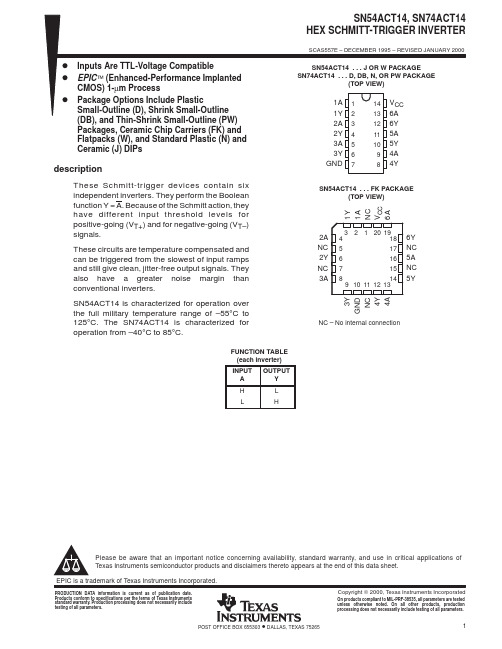
H EX S CHMITT-T RIGGER I NVERTERHigh-Speed Silicon-Gate CMOSThe IN74ACT14 is identical in pinout to the LS/ALS14,HC/HCT14. The IN74ACT14 may be used as a level converter for interfacing TTL or NMOS outputs to High Speed CMOS inputs.The IN74ACT14 is useful to “square up” slow input rise and fall times. Due to the hysteresis voltage of the Schmitt trigger, the IN74ACT14 finds applications in noisy environments.•TTL/NMOS Compatible Input Levels•Outputs Directly Interface to CMOS, NMOS, and TTL •Operating Voltage Range: 4.5 to 5.5 V•Low Input Current: 1.0 µA; 0.1 µA @ 25°C•Outputs Source/Sink 24 mAORDERING INFORMATION IN74ACT14N PlasticIN74ACT14D SOICT A = -40° to 85° C for allpackagesLOGIC DIAGRAMPIN 14 =V CC PIN 7 = GNDPIN ASSIGNMENT FUNCTION TABLEInputs OutputA YL HH LMAXIMUM RATINGS*Symbol Parameter ValueUnit V CC DC Supply Voltage (Referenced to GND) -0.5 to +7.0 VV IN DC Input Voltage (Referenced to GND) -0.5 to V CC +0.5 VV OUT DC Output Voltage (Referenced to GND) -0.5 to V CC +0.5 VI IN DC Input Current, per Pin ±20 mAI OUT DC Output Sink/Source Current, per Pin ±50 mAI CC DC Supply Current, V CC and GND Pins ±50 mAP D Power Dissipation in Still Air, Plastic DIP+ SOIC Package+ 750500mWTstg Storage Temperature -65 to +150 °CT L Lead Temperature, 1 mm from Case for 10Seconds(Plastic DIP or SOIC Package)260 °C*Maximum Ratings are those values beyond which damage to the device may occur.Functional operation should be restricted to the Recommended Operating Conditions.+Derating - Plastic DIP: - 10 mW/°C from 65° to 125°CSOIC Package: : - 7 mW/°C from 65° to 125°CRECOMMENDED OPERATING CONDITIONSSymbol Parameter MinMaxUnit V CC DC Supply Voltage (Referenced to GND) 4.5 5.5 VV IN, V OUT DC Input Voltage, Output Voltage (Referenced toGND)0 V CC VT J Junction Temperature (PDIP) 140 °CT A Operating Temperature, All Package Types -40 +85 °CI OH Output Current - High -24 mAI OL Output Current - Low 24 mAt r, t f Input Rise and Fall Time * (except Schmitt Inputs) V CC=4.5 VV CC =5.5 V108.0ns/V* VINfrom 0.8 V to 2.0 VThis device contains protection circuitry to guard against damage due to high static voltages or electric fields. However, precautions must be taken to avoid applications of any voltage higher than maximum rated voltages to this high-impedance circuit. For proper operation, V IN and V OUT should be constrained to the range GND≤(V IN or V OUT)≤V CC.Unused inputs must always be tied to an appropriate logic voltage level (e.g., either GND or V CC). Unused outputs must be left open.DC ELECTRICAL CHARACTERISTICS (Voltages Referenced to GND)V CCGuaranteed LimitsSymbol Parameter Test Conditions V 25 °C -40°Cto 85°CUnit V OH Minimum High-Level Output VoltageI OUT ≤ -50 µA 4.55.5 4.4 5.4 4.45.4 V *V IN ≤ V T - minI OH =-12 mA I OH =-24 mA I OH =-24 mA4.55.5 3.86 4.863.764.76V OL Maximum Low-Level Output VoltageI OUT ≤ 50 µA 4.55.5 0.1 0.1 0.10.1 V *V IN =≥ V T +maxI OL =12 mAI OL =24 mA I OL =24 mA4.55.5 0.36 0.360.44 0.44V T +max Maximum Positive-Going Input Threshold VoltageV OUT =0.1 V T A = Worst Case 4.55.5 2.0 2.0V V T - min Minimum Negative-Going Input Threshold VoltageV OUT = V CC - 0.1 V T A = Worst Case 4.55.5 0.80.8V V H max Maximum Hysteresis Voltage V OUT =0.1 V or V CC - 0.1 VT A = Worst Case4.55.5 1.2 1.2 V V H min Minimum Hysteresis Voltage V OUT =0.1 V or V CC - 0.1 VT A = Worst Case4.55.5 0.4 0.4 VI IN Maximum Input Leakage CurrentV IN =V CC or GND 5.5 ±0.1 ±1.0µA ∆I CCAddition Quiescent Supply CurrentV IN =V CC -2.1 V 5.5 1.5 mA I OLD +Minimum Dynamic Output CurrentV OLD =1.65 V Max 5.5 75mA I OHD +Minimum Dynamic Output CurrentV OHD =3.85 V Min 5.5 -75mAI CC Maximum Quiescent Supply Current(per Package)V IN =V CC or GND 5.5 4.0 40µAAll outputs loaded; thresholds on input associated with output under test. +Maximum test duration 2.0 ms, one output loaded at a time. Note: V H =(V T +)-(V T -).AC ELECTRICAL CHARACTERISTICS(V CC=5.0 V ± 10%, C L=50pF,Input t r=t f=3.0 ns)LimitsGuaranteedUnitSymbol Parameter 25 °C -40°C to85°CMaxMax MinMin1.5 11.5 1.0 12.5 nst PLH Propagation Delay, Input A to Output Y(Figure 1)t PHL Propagation Delay, Input A to Output Y1.5 10.0 1.0 11.0 ns(Figure 1)C IN Maximum Input Capacitance 4.5 4.5 pFTypical @25°C,V CC=5.0VC PD Power Dissipation Capacitance 25 pFFigure 1. Switching Waveforms。
TC74ACT74FT资料

TOSHIBA CMOS Digital Integrated Circuit Silicon Monolithic TC74ACT74P,TC74ACT74F,TC74ACT74FN,TC74ACT74FT Dual D-Type Flip Flop with Preset and ClearThe TC74ACT74 is an advanced high speed CMOS D-FLIP FLOP fabricated with silicon gate and double-layer metal wiring C2MOS technology.It achieves the high speed operation similar to equivalent Bipolar Schottky TTL while maintaining the CMOS low power dissipation.This device may be used as a level converter for interfacing TTL or NMOS to High Speed CMOS. The inputs are compatible with TTL, NMOS and CMOS output voltage levels.The signal level applied to the D INPUT is transferred to Q OUTPUT during the positive going transition of the CK pulse. CLR and PR are independent of the CK and are accomplished by setting the appropriate input to an “L” level. All inputs are equipped with protection circuits against static discharge or transient excess voltage.Features•High speed: f max = 180 MHz (typ.) at V CC = 5 V•Low power dissipation: I CC = 4 μA (max) at Ta = 25°C •Compatible with TTL outputs: V IL = 0.8 V (max)V IH = 2.0 V (min) •Symmetrical output impedance: |I OH| = I OL = 24 mA (min)Capability of driving 50 Ωtransmission lines. •Balanced propagation delays: t pLH ∼ − t pHL•Pin and function compatible with 74F74 Note: xxxFN (JEDEC SOP) is not available in Japan.TC74ACT74PTC74ACT74FTC74ACT74FNTC74ACT74FTWeightDIP14-P-300-2.54 : 0.96 g (typ.) SOP14-P-300-1.27A : 0.18 g (typ.) SOL14-P-150-1.27 : 0.12 g (typ.) TSSOP14-P-0044-0.65A : 0.06 g (typ.)Pin AssignmentIEC Logic SymbolTruth TableX: Don’t careSystem DiagramQ 1PR1V CCCLR 22D 2CK PR 2 2QCLR11D 1CK1QQ 29 814 13 12 11 10 (top view) GNDCLR2CLR 1(12)(3)S (4)(1)(2)(11)(10)1CK PR 11D 2CK 2D (5) (6) (9) (8)1QQ 12QQ2C11D R(13)PR 2DCLR CKPRQQφϕAbsolute Maximum Ratings (Note 1)Characteristics Symbol Rating Unit Supply voltage range V CC−0.5 to 7.0 VDC input voltage V IN−0.5 to V CC + 0.5 VDC output voltage V OUT−0.5 to V CC + 0.5 VmA Input diode current I IK ±20Output diode current I OK ±50 mA DC output current I OUT ±50 mA DC V CC/ground current I CC ±100 mA Power dissipation P D500 (DIP) (Note 2)/180 (SOP/TSSOP) mWStorage temperature T stg−65 to 150 °CNote 1: Exceeding any of the absolute maximum ratings, even briefly, lead to deterioration in IC performance or even destruction.Using continuously under heavy loads (e.g. the application of high temperature/current/voltage and thesignificant change in temperature, etc.) may cause this product to decrease in the reliability significantlyeven if the operating conditions (i.e. operating temperature/current/voltage, etc.) are within the absolutemaximum ratings and the operating ranges.Please design the appropriate reliability upon reviewing the Toshiba Semiconductor Reliability Handbook(“Handling Precautions”/“Derating Concept and Methods”) and individual reliability data (i.e. reliability testreport and estimated failure rate, etc).Note 2: 500 mW in the range of Ta = −40°C to 65°C. From Ta = 65°C to 85°C a derating factor of −10 mW/°C should be applied up to 300 mW.Operating Ranges (Note)Characteristics Symbol Rating Unit Supply voltage V CC 4.5 to 5.5 VInput voltage V IN0 to V CC VOutput voltage V OUT0 to V CC VOperating temperature T opr−40 to 85 °CInput rise and fall time dt/dV 0 to 10 ns/VNote: The operating ranges must be maintained to ensure the normal operation of the device.Unused inputs must be tied to either VCC or GND.Electrical CharacteristicsDC CharacteristicsTest ConditionTa = 25°CTa = −40 to 85°CCharacteristics SymbolV CC (V)Min Typ.Max Min MaxUnitHigh-level input voltage V IH― 4.5 to 5.5 2.0―― 2.0 ― VLow-level input voltageV IL―4.5 to5.5― ― 0.8 ― 0.8 V High-level output voltageV OHV IN= V IH or V ILI OH = −50 μAI OH = −24 mA I OH = −75 mA (Note) 4.54.55.5 4.4 3.94― 4.5 ― ― ― ― ― 4.4 3.80 3.85 ― ― ― VLow-level output voltage V OLVIN= V IH or V ILI OL = 50 μAI OL = 24 mA I OL = 75 mA (Note) 4.54.55.5― ― ― 0.0 ― ―0.1 0.36 ―― ― ―0.1 0.441.65V Input leakage currentI IN V IN = V CC or GND 5.5― ― ±0.1 ― ±1.0μA I CC V IN = V CC or GND 5.5― ― 4.0 ― 40.0μA Quiescent supply currentI CPer input: V IN = 3.4 V Other input: V CC or GND5.5―― 1.35 ― 1.5 mANote: This spec indicates the capability of driving 50 Ω transmission lines. One output should be tested at a time for a 10 ms maximum duration.Timing Requirements (input: t r = t f = 3 ns)AC Characteristics (C L = 50 pF, R L = 500 Ω, input: t r = t f = 3 ns)Note: C PD is defined as the value of the internal equivalent capacitance which is calculated from the operating current consumption without load.Average operating current can be obtained by the equation:I CC (opr) = C PD·V CC·f IN + I CC/2 (per F/F)Weight: 0.96 g (typ.)Weight: 0.18 g (typ.)Package Dimensions (Note)Note: This package is not available in Japan. Weight: 0.12 g (typ.)Package DimensionsWeight: 0.06 g (typ.)RESTRICTIONS ON PRODUCT USE20070701-EN GENERAL •The information contained herein is subject to change without notice.•TOSHIBA is continually working to improve the quality and reliability of its products. Nevertheless, semiconductor devices in general can malfunction or fail due to their inherent electrical sensitivity and vulnerability to physical stress. It is the responsibility of the buyer, when utilizing TOSHIBA products, to comply with the standards of safety in making a safe design for the entire system, and to avoid situations in which a malfunction or failure of such TOSHIBA products could cause loss of human life, bodily injury or damage to property.In developing your designs, please ensure that TOSHIBA products are used within specified operating ranges as set forth in the most recent TOSHIBA products specifications. Also, please keep in mind the precautions and conditions set forth in the “Handling Guide for Semiconductor Devices,” or “TOSHIBA Semiconductor Reliability Handbook” etc.• The TOSHIBA products listed in this document are intended for usage in general electronics applications (computer, personal equipment, office equipment, measuring equipment, industrial robotics, domestic appliances, etc.).These TOSHIBA products are neither intended nor warranted for usage in equipment that requires extraordinarily high quality and/or reliability or a malfunction or failure of which may cause loss of human life or bodily injury (“Unintended Usage”). Unintended Usage include atomic energy control instruments, airplane or spaceship instruments, transportation instruments, traffic signal instruments, combustion control instruments, medical instruments, all types of safety devices, etc.. Unintended Usage of TOSHIBA products listed in his document shall be made at the customer’s own risk.•The products described in this document shall not be used or embedded to any downstream products of which manufacture, use and/or sale are prohibited under any applicable laws and regulations.• The information contained herein is presented only as a guide for the applications of our products. No responsibility is assumed by TOSHIBA for any infringements of patents or other rights of the third parties which may result from its use. No license is granted by implication or otherwise under any patents or other rights of TOSHIBA or the third parties.• Please contact your sales representative for product-by-product details in this document regarding RoHS compatibility. Please use these products in this document in compliance with all applicable laws and regulations that regulate the inclusion or use of controlled substances. Toshiba assumes no liability for damage or losses occurring as a result of noncompliance with applicable laws and regulations.。
74ACT541_01中文资料

1/9April 2001s HIGH SPEED: t PD = 4ns (TYP .) at V CC = 5V sLOW POWER DISSIPATION:I CC = 4µA(MAX.) at T A =25°CsCOMPATIBLE WITH TTL OUTPUTS V IH = 2V (MIN.), V IL = 0.8V (MAX.)s50Ω TRANSMISSION LINE DRIVING CAPABILITYsSYMMETRICAL OUTPUT IMPEDANCE:|I OH | = I OL = 24mA (MIN)sBALANCED PROPAGATION DELAYS:t PLH ≅ t PHLsOPERATING VOLTAGE RANGE:V CC (OPR) = 4.5V to 5.5VsPIN AND FUNCTION COMPATIBLE WITH 74 SERIES 541sIMPROVED LATCH-UP IMMUNITYDESCRIPTIONThe 74ACT541 is an advanced high-speed CMOS OCTAL BUS BUFFER (3-STATE) fabricated with sub-micron silicon gate and double-layer metal wiring C 2MOS tecnology.The 3 STATE control gate operates as two input AND such that if either G1 and G2 are high, all eight outputs are in the high impedance state.In order to enhance PC board layout, the74ACT541 offers a pinout having inputs and outputs on opposite sides of the package.This device is designed to interface directly High Speed CMOS systems with TTL, NMOS and CMOS output voltage levlels.All inputs and outputs are equipped with protection circuits against static discharge, giving them 2KV ESD immunity and transient excess voltage.74ACT541OCTAL BUS BUFFERWITH 3 STATE OUTPUTS (NON INVERTED)PIN CONNECTION AND IEC LOGIC SYMBOLSORDER CODESPACKAGE TUBE T & R DIP 74ACT541B SOP 74ACT541M74ACT541MTR TSSOP74ACT541TTR74ACT5412/9INPUT AND OUTPUT EQUIVALENT CIRCUITPIN DESCRIPTIONTRUTH TABLEX : Don’t CareZ : High ImpedanceABSOLUTE MAXIMUM RATINGSAbsolute Maximum Ratings are those values beyond which damage to the device may occur. Functional operation under these conditions is not implied.RECOMMENDED OPERATING CONDITIONS1) V IN from 0.8V to 2.0VPIN No SYMBOL NAME AND FUNCTION 1, 19G1, G2Output Enable Inputs 2, 3, 4, 5, 6, 7, 8, 9A1 to A8Data Inputs 18, 17, 16, 15, 14, 13, 12, 11Y1 to Y8Data Outputs10GND Ground (0V)20V CCPositive Supply VoltageINPUTSOUTPUTG1G2An Yn H X X Z X H X Z L L H H LLLLSymbol ParameterValue Unit V CC Supply Voltage -0.5 to +7V V I DC Input Voltage -0.5 to V CC + 0.5V V O DC Output Voltage -0.5 to V CC + 0.5V I IK DC Input Diode Current ± 20mA I OK DC Output Diode Current ± 20mA I ODC Output Current± 50mA I CC or I GND DC V CC or Ground Current± 400mA T stg Storage Temperature-65 to +150°C T LLead Temperature (10 sec)300°CSymbol ParameterValue Unit V CC Supply Voltage 4.5 to 5.5V V I Input Voltage 0 to V CC V V O Output Voltage 0 to V CC V T op Operating Temperature-55 to 125°C dt/dvInput Rise and Fall Time V CC = 4.5 to 5.5V (note 1)8ns/V74ACT5413/9DC SPECIFICATIONS1) Maximum test duration 2ms, one output loaded at time2) Incident wave switching is guaranteed on transmission lines with impedances as low as 50ΩAC ELECTRICAL CHARACTERISTICS (C L = 50 pF, R L = 500 Ω, Input t r = t f = 3ns)(*) Voltage range is 5.0V ± 0.5VSymbolParameterTest ConditionValue UnitV CC (V)T A = 25°C -40 to 85°C -55 to 125°C Min.Typ.Max.Min.Max.Min.Max.V IH High Level Input Voltage4.5V O = 0.1 V or V CC -0.1V 2.0 1.5 2.0 2.0V5.5 2.01.52.02.0V IL Low Level Input Voltage4.5V O = 0.1 V or V CC -0.1V 1.50.80.80.85.5 1.50.80.80.8VV OHHigh Level Output Voltage4.5I O =-50 µA 4.4 4.49 4.4 4.45.5I O =-50 µA 5.4 5.495.4 5.44.5I O =-24 mA 3.86 3.76 3.7V5.5I O =-24 mA 4.864.764.7V OLLow Level Output Voltage4.5I O =50 µA 0.0010.10.10.15.5I O =50 µA 0.0010.10.10.14.5I O =24 mA 0.360.440.55.5I O =24 mA 0.360.440.5I I Input Leakage Cur-rent5.5V I = V CC or GND ± 0.1± 1± 1µA I OZ High Impedance Output Leakege Current5.5V I = V IH or V IL V O = V CC or GND ± 0.5± 5± 5µA I CCT Max I CC /Input 5.5V I = V CC - 2.1V 0.61.5 1.6mA I CC Quiescent Supply Current5.5V I = V CC or GND 44080µA I OLD Dynamic Output Current (note 1, 2)5.5V OLD = 1.65 V max 7550mA I OHDV OHD = 3.85 V min-75-50mA SymbolParameterTest ConditionValue UnitV CC (V)T A = 25°C -40 to 85°C -55 to 125°C Min.Typ.Max.Min.Max.Min.Max.t PLH t PHL Propagation DelayTime5.0(*) 1.5 4.06.5 1.58.0 1.58.0ns t PZL t PZH Output EnableTime5.0(*) 1.56.07.8 1.59.0 1.59.0ns t PLZ t PHZ Output DisableTime5.0(*)1.55.07.81.59.01.59.0ns74ACT5414/9CAPACITIVE CHARACTERISTICSPD load. (Refer to Test Circuit). Average operating current can be obtained by the following equation. I CC(opr) = C PD x V CC x f IN + I CC /n (per circuit)TEST CIRCUITC L = 50pF or equivalent (includes jig and probe capacitance)R L = R 1 = 500Ω or equivalentR T = Z OUT of pulse generator (typically 50Ω)SymbolParameterTest ConditionValue UnitV CC (V)T A = 25°C -40 to 85°C -55 to 125°C Min.Typ.Max.Min.Max.Min.Max.C IN Input Capacitance 5.04pF C OUT OutputCapacitance5.08pF C PDPower Dissipation Capacitance (note 1)5.0f IN = 10MHz22pF TESTSWITCH t PLH , t PHL Open t PZL , t PLZ 2V CC t PZH , t PHZOpen74ACT5415/9WAVEFORM 1: PROPAGATION DELAYS (f=1MHz; 50% duty cycle)WAVEFORM 2: OUTPUT ENABLE AND DISABLE TIME(f=1MHz; 50% duty cycle)74ACT541 Information furnished is believed to be accurate and reliable. However, STMicroelectronics assumes no responsibility for the consequences of use of such information nor for any infringement of patents or other rights of third parties which may result from its use. No license is granted by implication or otherwise under any patent or patent rights of STMicroelectronics. Specifications mentioned in this publication are subject to change without notice. This publication supersedes and replaces all information previously supplied. STMicroelectronics products are not authorized for use as critical components in life support devices or systems without express written approval of STMicroelectronics.© The ST logo is a registered trademark of STMicroelectronics© 2001 STMicroelectronics - Printed in Italy - All Rights ReservedSTMicroelectronics GROUP OF COMPANIESAustralia - Brazil - China - Finland - France - Germany - Hong Kong - India - Italy - Japan - Malaysia - Malta - MoroccoSingapore - Spain - Sweden - Switzerland - United Kingdom© 9/9。
MC74ACT14DR2G中文资料

MC74AC14, MC74ACT14 Hex Inverter Schmitt TriggerThe MC74AC14/74ACT14 contains six logic inverters which accept standard CMOS Input signals (TTL levels for MC74ACT14) and provide standard CMOS output levels. They are capable of transforming slowly changing input signals into sharply defined, jitter−free output signals. In addition, they have a greater noise margin then conventional inverters.The MC74AC14/74ACT14 has hysteresis between the positive−going and negative−going input thresholds (typically 1.0 V) which is determined internally by transistor ratios and is essentially insensitive to temperature and supply voltage variations.Features•Schmitt Trigger Inputs•Outputs Source/Sink 24 mA•′ACT14 Has TTL Compatible Inputs•Pb−Free Packages are AvailableMAXIMUM RATINGSRating Symbol ValueUnit DC Supply Voltage (Referenced to GND)V CC−0.5 to +7.0V DC Input Voltage (Referenced to GND)V in−0.5 to V CC +0.5V DC Output Voltage (Referenced to GND)V out−0.5 to V CC +0.5V DC Input Current, per Pin I in±20mA DC Output Sink/Source Current, per Pin I out±50mA DC V CC or GND Current per Output Pin I CC±50°C Storage Temperature T stg−65 to +150mJ Stresses exceeding Maximum Ratings may damage the device. Maximum Ratings are stress ratings only. Functional operation above the Recommended Operating Conditions is not implied. Extended exposure to stresses above the Recommended Operating Conditions may affect device reliability.SOEIAJ−14SUFFIX MCASE 965TSSOP−14SUFFIX DTCASE 948GSOIC−14SUFFIX DCASE 751APDIP−14SUFFIX NCASE 646See detailed ordering and shipping information in the package dimensions section on page 4 of this data sheet.ORDERING INFORMATIONSee general marking information in the device marking section on page 5 of this data sheet.DEVICE MARKING INFORMATION(Top View)Figure 1. Pinout: 14−Lead PackagesConductorsFUNCTION TABLEInputAOutputOLHHLRECOMMENDED OPERATING CONDITIONSSymbol Parameter Min Typ Max UnitV CC Supply Voltage′AC 2.0 5.0 6.0V ′ACT 4.5 5.0 5.5V in, V out DC Input Voltage, Output Voltage (Ref. to GND)0−V CC Vt r, t f Input Rise and Fall Time (Note 1)′AC Devices except Schmitt InputsV CC @ 3.0 V−150−V CC @ 4.5 V−40−ns/VV CC @ 5.5 V−25−t r, t f Input Rise and Fall Time (Note 2)′ACT Devices except Schmitt InputsV CC @ 4.5 V−10−ns/VV CC @ 5.5 V−8.0−T J Junction Temperature (PDIP)−−140°C T A Operating Ambient Temperature Range−402585°CI OH Output Current − High−−−24mAI OL Output Current − Low−−24mA1.V in from 30% to 70% V CC; see individual Data Sheets for devices that differ from the typical input rise and fall times.2.V in from 0.8 V to 2.0 V; see individual Data Sheets for devices that differ from the typical input rise and fall times.DC CHARACTERISTICSSymbol Parameter V CC(V)74AC74ACUnit Conditions T A = +25°C T A = −40°C to +85°CTyp Guaranteed LimitsV OH Minimum High Level Output Voltage 3.0 2.99 2.9 2.9I OUT = −50 m A4.5 4.49 4.4 4.4V5.5 5.49 5.4 5.4V *V IN = V IL or V IH3.0− 2.56 2.46−12 mA4.5− 3.86 3.76I OH−24 mA5.5− 4.86 4.76−24 mA V OL Maximum Low Level Output Voltage 3.00.0020.10.1I OUT = 50 m A4.50.0010.10.1V5.50.0010.10.1V *V IN = V IL or V IH3.0−0.360.4412 mA4.5−0.360.44I OL24 mA5.5−0.360.4424 mAI IN Maximum Input Leakage Current5.5−±0.1±1.0m A V I = V CC, GNDI OLD†Minimum Dynamic Output Current 5.5−−75mA V OLD = 1.65 V MaxI OHD 5.5−−−75mA V OHD = 3.85 V MinI CC Maximum Quiescent Supply Current 5.5− 4.040m A V IN = V CC or GND *All outputs loaded; thresholds on input associated with output under test.†Maximum test duration 2.0 ms, one output loaded at a time.NOTE:I IN and I CC @ 3.0 V are guaranteed to be less than or equal to the respective limit @ 5.5 V V CC.AC CHARACTERISTICS(For Figures and Waveforms − See Section 3 of the ON Semiconductor FACT Data Book, DL138/D)Symbol Parameter V CC*(V)74AC74ACUnitFigureNo.T A = +25°C C L = 50 pFT A = −40°C to+85°C C L = 50 pFMin Typ Max Min Maxt PLH Propagation Delay 3.3 1.59.513.5 1.515.0ns3−5 5.0 1.57.010.0 1.511.0t PHL Propagation Delay 3.3 1.57.511.5 1.513.0ns3−5 5.0 1.5 6.08.5 1.59.5*Voltage Range 3.3 V is 3.3 V ±0.3 V. Voltage Range 5.0 V is 5.0 V ±0.5 V.INPUT CHARACTERISTICS (unless otherwise specified)Symbol Parameter V CC(V)74AC74ACT Test ConditionsMaximum Positive Threshold 3.0 2.2V t+ 4.5 3.2 2.0V T A = Worst Case5.5 3.9Minimum Negative Threshold 3.00.5V t− 4.50.90.8V T A = Worst Case5.5 1.13.0 1.2V h(max)Maximum Hysteresis 4.5 1.4 1.2V T A = Worst Case5.5 1.63.00.3V h(min)Minimum Hysteresis 4.50.40.4V T A = Worst Case5.50.5DC CHARACTERISTICSSymbol Parameter V CC(V)74ACT74ACTUnit Conditions T A = +25°C T A = −40°C to +85°CTyp Guaranteed LimitsV OH Minimum High Level Output Voltage 4.5 4.49 4.4 4.4V I OUT = −50 m A5.5 5.49 5.4 5.4*V IN = V IL or V IH4.5− 3.86 3.76V I OH−24 mA5.5− 4.86 4.76−24 mAV OL Maximum Low Level Output Voltage 4.50.0010.10.1V I OUT = 50 m A5.50.0010.10.1*V IN = V IL or V IH4.5−0.360.44VI OL 24 mA5.5−0.360.4424 mAI IN Maximum Input Leakage Current5.5−±0.1±1.0m A V I = V CC, GNDD I CCT Additional Max. I CC/Input 5.50.6− 1.5mA V I = V CC−2.1 VI OLD†Minimum Dynamic Output Current 5.5−−75mA V OLD = 1.65 V MaxI OHD 5.5−−−75mA V OHD = 3.85 V MinI CC Maximum Quiescent Supply Current 5.5− 4.040m A V IN = V CC or GND *All outputs loaded; thresholds on input associated with output under test.†Maximum test duration 2.0 ms, one output loaded at a time.AC CHARACTERISTICS(For Figures and Waveforms − See Section 3 of the ON Semiconductor FACT Data Book, DL138/D)Symbol Parameter V CC*(V)74ACT74ACTUnitFigureNo.T A = +25°C C L = 50 pFT A = −40°C to+85°C C L = 50 pFMin Typ Max Min Maxt PLH Propagation Delay 5.0 1.5−11.5 1.012.5ns3−5 t PHL Propagation Delay 5.0 1.5−10.0 1.011.0ns3−5 *Voltage Range 5.0 V is 5.0 V ±0.5 V.CAPACITANCESymbol Parameter Value Typ Unit Test ConditionsC IN Input Capacitance 4.5pF V CC = 5.0 VC PD Power Dissipation Capacitance25pF V CC = 5.0 VORDERING INFORMATIONDevicePackage Shipping †MC74AC14N PDIP −1425 Units / RailMC74AC14NG PDIP −14(Pb −Free)MC74ACT14N PDIP −14MC74ACT14NG PDIP −14(Pb −Free)MC74AC14D SOIC −1455 Units / Rail MC74AC14DG SOIC −14(Pb −Free)MC74AC14DR2SOIC −142500 / Tape & Reel MC74AC14DR2G SOIC −14(Pb −Free)MC74ACT14D SOIC −1455 Units / Rail MC74ACT14DG SOIC −14(Pb −Free)MC74ACT14DR2SOIC −142500 / Tape & Reel MC74ACT14DR2G SOIC −14(Pb −Free)MC74AC14DTR2TSSOP −14*MC74AC14DTR2G TSSOP −14*MC74ACT14DTR2TSSOP −14*MC74ACT14DTR2G TSSOP −14*MC74AC14MEL SOEIAJ −142000 / Tape & ReelMC74AC14MELG SOEIAJ −14(Pb −Free)MC74ACT14MEL SOEIAJ −14MC74ACT14MELGSOEIAJ −14(Pb −Free)†For information on tape and reel specifications, including part orientation and tape sizes, please refer to our Tape and Reel Packaging Specifications Brochure, BRD8011/D.*This package is inherently Pb −Free.MARKING DIAGRAMSSOEIAJ −1474AC14ALYWG TSSOP −14SOIC −14AC 14ALYW G G A =Assembly Location WL, L =Wafer LotYY, Y =YearWW, W =Work Week G or G = Pb −Free Package(Note: Microdot may be in either location)PDIP −14MC74AC14N AWLYYWWG 11411411474ACT14ALYWG ACT 14ALYW G GMC74ACT14N AWLYYWWG 114114114PACKAGE DIMENSIONSPDIP−14CASE 646−06ISSUE PPACKAGE DIMENSIONSSOIC −14CASE 751A −03ISSUE HNOTES:1.DIMENSIONING AND TOLERANCING PER ANSI Y14.5M, 1982.2.CONTROLLING DIMENSION: MILLIMETER.3.DIMENSIONS A AND B DO NOT INCLUDE MOLD PROTRUSION.4.MAXIMUM MOLD PROTRUSION 0.15 (0.006)PER SIDE.5.DIMENSION D DOES NOT INCLUDE DAMBAR PROTRUSION. ALLOWABLE DAMBAR PROTRUSION SHALL BE 0.127(0.005) TOTAL IN EXCESS OF THE D DIMENSION AT MAXIMUM MATERIAL CONDITION.DIM MIN MAX MIN MAX INCHESMILLIMETERS A 8.558.750.3370.344B 3.80 4.000.1500.157C 1.35 1.750.0540.068D 0.350.490.0140.019F 0.40 1.250.0160.049G 1.27 BSC 0.050 BSC J 0.190.250.0080.009K 0.100.250.0040.009M 0 7 0 7 P 5.80 6.200.2280.244R0.250.500.0100.019____DIMENSIONS: MILLIMETERS*For additional information on our Pb −Free strategy and soldering details, please download the ON Semiconductor Soldering and Mounting Techniques Reference Manual, SOLDERRM/D.PACKAGE DIMENSIONSTSSOP −14CASE 948G −01ISSUE BDIM MIN MAX MIN MAX INCHESMILLIMETERS A 4.90 5.100.1930.200B 4.30 4.500.1690.177C −−− 1.20−−−0.047D 0.050.150.0020.006F 0.500.750.0200.030G 0.65 BSC 0.026 BSC H 0.500.600.0200.024J 0.090.200.0040.008J10.090.160.0040.006K 0.190.300.0070.012K10.190.250.0070.010L 6.40 BSC 0.252 BSC M0 8 0 8 NOTES:1.DIMENSIONING AND TOLERANCING PER ANSI Y14.5M, 1982.2.CONTROLLING DIMENSION: MILLIMETER.3.DIMENSION A DOES NOT INCLUDE MOLD FLASH, PROTRUSIONS OR GATE BURRS.MOLD FLASH OR GATE BURRS SHALL NOT EXCEED 0.15 (0.006) PER SIDE.4.DIMENSION B DOES NOT INCLUDE INTERLEAD FLASH OR PROTRUSION.INTERLEAD FLASH OR PROTRUSION SHALL NOT EXCEED 0.25 (0.010) PER SIDE.5.DIMENSION K DOES NOT INCLUDE DAMBAR PROTRUSION. ALLOWABLE DAMBARPROTRUSION SHALL BE 0.08 (0.003) TOTAL IN EXCESS OF THE K DIMENSION AT MAXIMUM MATERIAL CONDITION.6.TERMINAL NUMBERS ARE SHOWN FOR REFERENCE ONLY .7.DIMENSION A AND B ARE TO BEDETERMINED AT DATUM PLANE −W −.____14X0.360.65PITCHSOLDERING FOOTPRINT**For additional information on our Pb −Free strategy and soldering details, please download the ON Semiconductor Soldering and Mounting Techniques Reference Manual, SOLDERRM/D.PACKAGE DIMENSIONSSOEIAJ −14M SUFFIX CASE 965−01ISSUE AON Semiconductor and are registered trademarks of Semiconductor Components Industries, LLC (SCILLC). SCILLC reserves the right to make changes without further notice to any products herein. SCILLC makes no warranty, representation or guarantee regarding the suitability of its products for any particular purpose, nor does SCILLC assume any liability arising out of the application or use of any product or circuit, and specifically disclaims any and all liability, including without limitation special, consequential or incidental damages.“Typical” parameters which may be provided in SCILLC data sheets and/or specifications can and do vary in different applications and actual performance may vary over time. All operating parameters, including “Typicals” must be validated for each customer application by customer’s technical experts. SCILLC does not convey any license under its patent rights nor the rights of others. SCILLC products are not designed, intended, or authorized for use as components in systems intended for surgical implant into the body, or other applications intended to support or sustain life, or for any other application in which the failure of the SCILLC product could create a situation where personal injury or death may occur. Should Buyer purchase or use SCILLC products for any such unintended or unauthorized application, Buyer shall indemnify and hold SCILLC and its officers, employees, subsidiaries, affiliates,and distributors harmless against all claims, costs, damages, and expenses, and reasonable attorney fees arising out of, directly or indirectly, any claim of personal injury or death associated with such unintended or unauthorized use, even if such claim alleges that SCILLC was negligent regarding the design or manufacture of the part. SCILLC is an Equal Opportunity/Affirmative Action Employer. This literature is subject to all applicable copyright laws and is not for resale in any manner.PUBLICATION ORDERING INFORMATION。
74系列各个芯片详细介绍
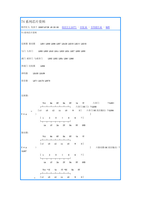
74系列芯片资料程序匠人发表于 2005-10-29 19:20:00 阅读全文(2477) | 回复(0) | 引用通告(0) | 编辑74系列芯片资料反相器驱动器 LS04 LS05 LS06 LS07 LS125 LS240 LS244 LS245与门与非门 LS00 LS08 LS10 LS11 LS20 LS21 LS27 LS30 LS38或门或非门与或非门 LS02 LS32 LS51 LS64 LS65异或门比较器 LS86译码器 LS138 LS139寄存器 LS74 LS175 LS373反相器:Vcc 6A 6Y 5A 5Y 4A 4Y 六非门 74LS04┌┴─┴─┴─┴─┴─┴─┴┐六非门(OC门) 74LS05_ │14 13 12 11 10 9 8│六非门(OC高压输出) 74LS06Y = A )││ 1 2 3 4 5 6 7│└┬─┬─┬─┬─┬─┬─┬┘1A 1Y 2A 2Y 3A 3Y GND驱动器:Vcc 6A 6Y 5A 5Y 4A 4Y┌┴─┴─┴─┴─┴─┴─┴┐│14 13 12 11 10 9 8│Y = A )│六驱动器(OC高压输出) 74LS07│ 1 2 3 4 5 6 7│└┬─┬─┬─┬─┬─┬─┬┘1A 1Y 2A 2Y 3A 3Y GNDVcc -4C 4A 4Y -3C 3A 3Y┌┴─┴─┴─┴─┴─┴─┴┐_ │14 13 12 11 10 9 8│Y =A+C )│四总线三态门 74LS125│ 1 2 3 4 5 6 7│└┬─┬─┬─┬─┬─┬─┬┘-1C 1A 1Y -2C 2A 2Y GNDVcc -G B1 B2 B3 B4 B8 B6 B7 B8┌┴─┴─┴─┴─┴─┴─┴─┴─┴─┴┐ 8位总线驱动器 74LS245 │20 19 18 17 16 15 14 13 12 11│)│ DIR=1 A=>B│ 1 2 3 4 5 6 7 8 9 10│ DIR=0 B=>A└┬─┬─┬─┬─┬─┬─┬─┬─┬─┬┘DIR A1 A2 A3 A4 A5 A6 A7 A8 GND页首非门,驱动器与门,与非门或门,或非门异或门,比较器译码器寄存器正逻辑与门,与非门:Vcc 4B 4A 4Y 3B 3A 3Y┌┴─┴─┴─┴─┴─┴─┴┐│14 13 12 11 10 9 8│Y = AB )│ 2输入四正与门 74LS08 │ 1 2 3 4 5 6 7│└┬─┬─┬─┬─┬─┬─┬┘1A 1B 1Y 2A 2B 2Y GNDVcc 4B 4A 4Y 3B 3A 3Y┌┴─┴─┴─┴─┴─┴─┴┐__ │14 13 12 11 10 9 8│Y = AB )│ 2输入四正与非门 74LS00 │ 1 2 3 4 5 6 7│└┬─┬─┬─┬─┬─┬─┬┘1A 1B 1Y 2A 2B 2Y GNDVcc 1C 1Y 3C 3B 3A 3Y┌┴─┴─┴─┴─┴─┴─┴┐___ │14 13 12 11 10 9 8│Y = ABC )│ 3输入三正与非门 74LS10 │ 1 2 3 4 5 6 7│└┬─┬─┬─┬─┬─┬─┬┘1A 1B 2A 2B 2C 2Y GNDVcc H G Y┌┴─┴─┴─┴─┴─┴─┴┐│14 13 12 11 10 9 8│)│ 8输入与非门 74LS30│ 1 2 3 4 5 6 7│ ________└┬─┬─┬─┬─┬─┬─┬┘ Y = ABCDEFGHA B C D E F GND页首非门,驱动器与门,与非门或门,或非门异或门,比较器译码器寄存器正逻辑或门,或非门:Vcc 4B 4A 4Y 3B 3A 3Y┌┴─┴─┴─┴─┴─┴─┴┐ 2输入四或门 74LS32│14 13 12 11 10 9 8│)│ Y = A+B│ 1 2 3 4 5 6 7│└┬─┬─┬─┬─┬─┬─┬┘1A 1B 1Y 2A 2B 2Y GNDVcc 4Y 4B 4A 3Y 3B 3A┌┴─┴─┴─┴─┴─┴─┴┐ 2输入四或非门 74LS02│14 13 12 11 10 9 8│ ___)│ Y = A+B│ 1 2 3 4 5 6 7│└┬─┬─┬─┬─┬─┬─┬┘1Y 1A 1B 2Y 2A 2B GNDVcc 2Y 2B 2A 2D 2E 1F┌┴─┴─┴─┴─┴─┴─┴┐双与或非门 74S51│14 13 12 11 10 9 8│ _____)│ 2Y = AB+DE│ 1 2 3 4 5 6 7│ _______└┬─┬─┬─┬─┬─┬─┬┘ 1Y = ABC+DEF1Y 1A 1B 1C 1D 1E GNDVcc D C B K J Y┌┴─┴─┴─┴─┴─┴─┴┐ 4-2-3-2与或非门 74S64 74S65(OC门) │14 13 12 11 10 9 8│ ______________)│ Y = ABCD+EF+GHI+JK│ 1 2 3 4 5 6 7│└┬─┬─┬─┬─┬─┬─┬┘A E F G H I GND页首非门,驱动器与门,与非门或门,或非门异或门,比较器译码器寄存器2输入四异或门 74LS86Vcc 4B 4A 4Y 3Y 3B 3A┌┴─┴─┴─┴─┴─┴─┴┐│14 13 12 11 10 9 8│)│ _ _│ 1 2 3 4 5 6 7│ Y=AB+AB└┬─┬─┬─┬─┬─┬─┬┘1A 1B 1Y 2Y 2A 2B GND8*2输入比较器 74LS688_Vcc Y B8 A8 B7 A7 B6 A6 B5 A5┌┴─┴─┴─┴─┴─┴─┴─┴─┴─┴┐ 8*2输入比较器 74LS688│20 19 18 17 16 15 14 13 12 11│)││ 1 2 3 4 5 6 7 8 9 10│└┬─┬─┬─┬─┬─┬─┬─┬─┬─┬┘CE A1 B1 A2 B2 A3 B3 A4 B4 GND_Y=A1⊙B1+A2⊙B2+A3⊙B3+A4⊙B4+A5⊙B5+A6⊙B6+A7⊙B7+A8⊙B8页首非门,驱动器与门,与非门或门,或非门异或门,比较器译码器寄存器3-8译码器 74LS138Vcc -Y0 -Y1 -Y2 -Y3 -Y4 -Y5 -Y6 __ _ _ _ __ _ _ __ _ _ __ _ ┌┴─┴─┴─┴─┴─┴─┴─┴┐ Y0=A B C Y1=A B B Y2=A B C Y3=A B C │16 15 14 13 12 11 10 9 │)│ __ _ _ __ _ __ _ __│ 1 2 3 4 5 6 7 8│ Y4=A B C Y5=A B C Y6=A B C Y7=A B C └┬─┬─┬─┬─┬─┬─┬─┬┘A B C -CS0 -CS1 CS2 -Y7 GND双2-4译码器 74LS139Vcc -2G 2A 2B -Y0 -Y1 -Y2 -Y3 __ __ __ __ __ __ __ __┌┴─┴─┴─┴─┴─┴─┴─┴┐ Y0=2A 2B Y1=2A 2B Y2=2A 2B Y3=2A 2B │16 15 14 13 12 11 10 9 │)│ __ __ __ __ __ __ __ __│ 1 2 3 4 5 6 7 8│ Y0=1A 1B Y1=1A 1B Y2=1A 1B Y3=1A 1B └┬─┬─┬─┬─┬─┬─┬─┬┘-1G 1A 1B -Y0 -Y1 -Y2 -Y3 GND8*2输入比较器 74LS688_Vcc Y B8 A8 B7 A7 B6 A6 B5 A5┌┴─┴─┴─┴─┴─┴─┴─┴─┴─┴┐ 8*2输入比较器 74LS688│20 19 18 17 16 15 14 13 12 11│)││ 1 2 3 4 5 6 7 8 9 10│└┬─┬─┬─┬─┬─┬─┬─┬─┬─┬┘CE A1 B1 A2 B2 A3 B3 A4 B4 GND_Y=A1⊙B1+A2⊙B2+A3⊙B3+A4⊙B4+A5⊙B5+A6⊙B6+A7⊙B7+A8⊙B8寄存器:Vcc 2CR 2D 2Ck 2St 2Q -2Q┌┴─┴─┴─┴─┴─┴─┴┐双D触发器 74LS74│14 13 12 11 10 9 8 │)││ 1 2 3 4 5 6 7│└┬─┬─┬─┬─┬─┬─┬┘1Cr 1D 1Ck 1St 1Q -1Q GNDVcc 8Q 8D 7D 7Q 6Q 6D 5D 5Q ALE┌┴─┴─┴─┴─┴─┴─┴─┴─┴─┴┐ 8位锁存器 74LS373│20 19 18 17 16 15 14 13 12 11│)││ 1 2 3 4 5 6 7 8 9 10│└┬─┬─┬─┬─┬─┬─┬─┬─┬─┬┘-OE 1Q 1D 2D 2Q 3Q 3D 4D 4Q GND型号器件名称厂牌[数据表]SN7400四2输入端与非门 TI[DATA]SN7401四2输入端与非门(OC) SN7402四2输入端或非门 TI[DATA]SN7403四2输入端与非门(OC)TI[DATA]SN7404六反相器 TI[DATA]SN7405六反相器(OC)TI[DATA]SN7406六高压输出反相器 (OC,30V)TI[DATA]SN7407六高压输出缓冲,驱动器(OC,30V)TI[DATA]SN7408四2输入端与门 TI[DATA]SN7409四2输入端与门(OC)TI[DATA]SN7410三3输入端与非门 TI[DATA]SN7412三3输入端与非门(OC)TI[DATA]SN7413双4输入端与非门 TI[DATA]SN7414六反相器TI[DATA]SN7416六高压输出反相缓冲/驱动器 I[DATA]SN7417六高压输出缓冲/驱动器(OC,15V)TI[DATA]SN7420双4输入端与非门 TI[DATA]SN7422双4输入端与非门(OC)TI[DATA]SN7423可扩展双4输入端或非门 TI[DATA]SN7425双4输入端或非门TI[DATA]SN7426四2输入端高压输出与非缓冲器 [DATA]SN7427三3输入端或非门TI[DATA]SN7428四2输入端或非缓冲器 I[DATA]SN74308输入端与非门TI[DATA]SN7432四2输入端或门。
常用74系列芯片

74系列集成电路大全74系列集成电路大致可分为6大类:74××(标准型);74LS××(低功耗肖特基);74S××(肖特基);74ALS××(先进低功耗肖特基);74AS××(先进肖特基);74F××(高速)。
HC为COMS工作电平;HCT为TTL工作电平,可与74LS系列互换使用;HCU适用于无缓冲级的CMOS电路。
这9种74系列产品,只要后边的标号相同,其逻辑功能和管脚排列就相同。
根据不同的条件和要求可选择不同类型的74系列产品,比如电路的供电电压为3V就应选择74HC系列的产品。
补充:.74 –系列这是早期的产品,现仍在使用,但正逐渐被淘汰。
2.74H –系列这是74 –系列的改进型,属于高速TTL产品。
其“与非门”的平均传输时间达10ns左右,但电路的静态功耗较大,目前该系列产品使用越来越少,逐渐被淘汰。
3.74S –系列这是TTL的高速型肖特基系列。
在该系列中,采用了抗饱和肖特基二极管,速度较高,但品种较少。
4.74LS –系列这是当前TTL类型中的主要产品系列。
品种和生产厂家都非常多。
性能价格比比较高,目前在中小规模电路中应用非常普遍。
5.74ALS –系列这是“先进的低功耗肖特基”系列。
属于74LS –系列的后继产品,速度(典型值为4ns)、功耗(典型值为1mW)等方面都有较大的改进,但价格比较高。
6.74AS –系列这是74S –系列的后继产品,尤其速度(典型值为1.5ns)有显著的提高,又称“先进超高速肖特基”系列。
7.74HC –系列54/74HC –系列是高速CMOS标准逻辑电路系列,具有与74LS –系列同等的工作度和CMOS集成电路固有的低功耗及电源电压范围宽等特点。
74HCxxx是74LSxxx同序号的翻版,型号最后几位数字相同,表示电路的逻辑功能、管脚排列完全兼容,为用74HC替代74LS提供了方便。
SN74ACT14D中文资料
元器件交易网IMPORTANT NOTICETexas Instruments and its subsidiaries (TI) reserve the right to make changes to their products or to discontinueany product or service without notice, and advise customers to obtain the latest version of relevant informationto verify, before placing orders, that information being relied on is current and complete. All products are soldsubject to the terms and conditions of sale supplied at the time of order acknowledgement, including thosepertaining to warranty, patent infringement, and limitation of liability.TI warrants performance of its semiconductor products to the specifications applicable at the time of sale inaccordance with TI’s standard warranty. Testing and other quality control techniques are utilized to the extentTI deems necessary to support this warranty. Specific testing of all parameters of each device is not necessarilyperformed, except those mandated by government requirements.CERTAIN APPLICATIONS USING SEMICONDUCTOR PRODUCTS MAY INVOLVE POTENTIAL RISKS OFDEATH, PERSONAL INJURY, OR SEVERE PROPERTY OR ENVIRONMENTAL DAMAGE (“CRITICALAPPLICATIONS”). TI SEMICONDUCTOR PRODUCTS ARE NOT DESIGNED, AUTHORIZED, ORWARRANTED TO BE SUITABLE FOR USE IN LIFE-SUPPORT DEVICES OR SYSTEMS OR OTHERCRITICAL APPLICATIONS. INCLUSION OF TI PRODUCTS IN SUCH APPLICATIONS IS UNDERSTOOD TOBE FULLY AT THE CUSTOMER’S RISK.In order to minimize risks associated with the customer’s applications, adequate design and operatingsafeguards must be provided by the customer to minimize inherent or procedural hazards.TI assumes no liability for applications assistance or customer product design. TI does not warrant or representthat any license, either express or implied, is granted under any patent right, copyright, mask work right, or otherintellectual property right of TI covering or relating to any combination, machine, or process in which suchsemiconductor products or services might be or are used. TI’s publication of information regarding any thirdparty’s products or services does not constitute TI’s approval, warranty or endorsement thereof.Copyright © 2000, Texas Instruments Incorporated。
- 1、下载文档前请自行甄别文档内容的完整性,平台不提供额外的编辑、内容补充、找答案等附加服务。
- 2、"仅部分预览"的文档,不可在线预览部分如存在完整性等问题,可反馈申请退款(可完整预览的文档不适用该条件!)。
- 3、如文档侵犯您的权益,请联系客服反馈,我们会尽快为您处理(人工客服工作时间:9:00-18:30)。
1/8April 2001s HIGH SPEED: t PD = 7.2 ns (TYP.) at V CC = 5V sLOW POWER DISSIPATION:I CC = 4µA(MAX.) at T A =25°Cs50Ω TRANSMISSION LINE DRIVING CAPABILITYsSYMMETRICAL OUTPUT IMPEDANCE:|I OH | = I OL = 24mA (MIN)sBALANCED PROPAGATION DELAYS:t PLH ≅ t PHLsOPERATING VOLTAGE RANGE:V CC (OPR) = 2V to 5.5VsPIN AND FUNCTION COMPATIBLE WITH 74 SERIES 14sIMPROVED LATCH-UP IMMUNITYDESCRIPTIONThe 74ACT14 is an advanced high-speed CMOS HEX SCHMITT INVERTER fabricated with sub-micron silicon gate and double-layer metal wiring C 2MOS tecnology.The internal circuit is composed of 3 stages including buffer output, which enables high noise immunity and stable output.The device is designed to interface directly High Speed CMOS systems with TTL, NMOS andCMOS output voltage levels.This together with its schmitt trigger function allows it to be used on line receivers with slow rise/fall input signals.All inputs and outputs are equipped with protec-tion circuits against static discharge, giving them 2KV ESD immunity and transient excess voltage.74ACT14HEX SCHMITT INVERTERPIN CONNECTION AND IEC LOGIC SYMBOLSORDER CODESPACKAGE TUBE T & R DIP 74ACT14B SOP 74ACT14M74ACT14MTR TSSOP74ACT14TTR74ACT142/8INPUT AND OUTPUT EQUIVALENT CIRCUITPIN DESCRIPTIONTRUTH TABLEABSOLUTE MAXIMUM RATINGSAbsolute Maximum Ratings are those values beyond which damage to the device may occur. Functional operation under these conditions is not implied.RECOMMENDED OPERATING CONDITIONS1) V IN from 0.8V to 2.0VPIN No SYMBOL NAME AND FUNCTION 1, 3, 5, 9, 11,131A to 6A Data Inputs 2, 4, 6, 8, 10,121Y to 6Y Data Outputs 7GND Ground (0V)14V CCPositive Supply VoltageA Y L H HLSymbol ParameterValue Unit V CC Supply Voltage -0.5 to +7V V I DC Input Voltage -0.5 to V CC + 0.5V V O DC Output Voltage -0.5 to V CC + 0.5V I IK DC Input Diode Current ± 20mA I OK DC Output Diode Current ± 20mA I ODC Output Current± 50mA I CC or I GND DC V CC or Ground Current± 300mA T stg Storage Temperature-65 to +150°C T LLead Temperature (10 sec)300°CSymbol ParameterValue Unit V CC Supply Voltage 4.5 to 5.5V V I Input Voltage 0 to V CC V V O Output Voltage 0 to V CC V T opOperating Temperature-55 to 125°C74ACT143/8DC SPECIFICATIONS1) Maximum test duration 2ms, one output loaded at time2) Incident wave switching is guaranteed on transmission lines with impedances as low as 50ΩAC ELECTRICAL CHARACTERISTICS (C L = 50 pF, R L = 500 Ω, Input t r = t f = 3ns)(*) Voltage range is 5.0V ± 0.5VCAPACITIVE CHARACTERISTICS1) C PD is defined as the value of the IC’s internal equivalent capacitance which is calculated from the operating current consumption without load. (Refer to Test Circuit). Average operating current can be obtained by the following equation. I CC(opr) = C PD x V CC x f IN + I CC /6 (per gate)SymbolParameterTest ConditionValue UnitV CC (V)T A = 25°C -40 to 85°C -55 to 125°C Min.Typ.Max.Min.Max.Min.Max.V t+High Level Input Voltage4.5 2.0 2.0 2.0V5.5 2.02.02.0V t-Low Level Input Voltage4.50.60.60.6V5.50.60.60.6V h Hysteresis Voltage 4.50.4 1.40.4 1.40.4 1.4V 5.50.4 1.50.4 1.50.4 1.5V OHHigh Level Output Voltage4.5I O =-50 µA 4.4 4.49 4.4 4.4V5.5I O =-50 µA 5.4 5.49 5.4 5.44.5I O =-24 mA 3.86 3.76 3.75.5I O =-24 mA 4.864.764.7V OLLow Level Output Voltage4.5I O =50 µA 0.0010.10.10.1V5.5I O =50 µA 0.0010.10.10.14.5I O =24 mA 0.360.440.55.5I O =24 mA 0.360.440.5I I Input Leakage Cur-rent5.5V I = V CC or GND ± 0.1± 1± 1µA I CCT Max I CC /Input 5.5V I = V CC - 2.1V 0.61.5 1.6mA I CC Quiescent Supply Current5.5V I = V CC or GND 44040µA I OLD Dynamic Output Current (note 1, 2)5.5V OLD = 1.65 V max 7550mA I OHDV OHD = 3.85 V min-75-50mA SymbolParameterTest ConditionValue UnitV CC (V)T A = 25°C -40 to 85°C -55 to 125°C Min.Typ.Max.Min.Max.Min.Max.t PLH t PHL Propagation DelayTime5.0(*)7.211.414.014.0ns SymbolParameterTest ConditionValue UnitV CC (V)T A = 25°C -40 to 85°C -55 to 125°C Min.Typ.Max.Min.Max.Min.Max.C IN Input Capacitance 5.05101010pF C PDPower Dissipation Capacitance (note 1)5.0f IN = 10MHz30pF74ACT144/8TEST CIRCUITC L = 50pF or equivalent (includes jig and probe capacitance)R L = R 1 = 500Ω or equivalentR T = Z OUT of pulse generator (typically 50Ω)WAVEFORM: PROPAGATION DELAYS(f=1MHz; 50% duty cycle)74ACT14Information furnished is believed to be accurate and reliable. However, STMicroelectronics assumes no responsibility for the consequences of use of such information nor for any infringement of patents or other rights of third parties which may result from its use. No license is granted by implication or otherwise under any patent or patent rights of STMicroelectronics. Specifications mentioned in this publication are subject to change without notice. This publication supersedes and replaces all information previously supplied. STMicroelectronics products are not authorized for use as critical components in life support devices or systems without express written approval of STMicroelectronics.© The ST logo is a registered trademark of STMicroelectronics© 2001 STMicroelectronics - Printed in Italy - All Rights ReservedSTMicroelectronics GROUP OF COMPANIESAustralia - Brazil - China - Finland - France - Germany - Hong Kong - India - Italy - Japan - Malaysia - Malta - MoroccoSingapore - Spain - Sweden - Switzerland - United Kingdom© 8/8。